CN102403406B - Preparation method for back contact type silicon solar cell - Google Patents
Preparation method for back contact type silicon solar cell Download PDFInfo
- Publication number
- CN102403406B CN102403406B CN2011103740324A CN201110374032A CN102403406B CN 102403406 B CN102403406 B CN 102403406B CN 2011103740324 A CN2011103740324 A CN 2011103740324A CN 201110374032 A CN201110374032 A CN 201110374032A CN 102403406 B CN102403406 B CN 102403406B
- Authority
- CN
- China
- Prior art keywords
- solar cell
- film
- sensitive surface
- nesa coating
- hole
- Prior art date
- Legal status (The legal status is an assumption and is not a legal conclusion. Google has not performed a legal analysis and makes no representation as to the accuracy of the status listed.)
- Active
Links
- XUIMIQQOPSSXEZ-UHFFFAOYSA-N Silicon Chemical compound [Si] XUIMIQQOPSSXEZ-UHFFFAOYSA-N 0.000 title claims abstract description 98
- 229910052710 silicon Inorganic materials 0.000 title claims abstract description 90
- 239000010703 silicon Substances 0.000 title claims abstract description 90
- 238000002360 preparation method Methods 0.000 title claims abstract description 20
- 239000011248 coating agent Substances 0.000 claims abstract description 30
- 238000000576 coating method Methods 0.000 claims abstract description 30
- 229910052751 metal Inorganic materials 0.000 claims abstract description 16
- 239000002184 metal Substances 0.000 claims abstract description 16
- 238000002161 passivation Methods 0.000 claims abstract description 14
- 238000009792 diffusion process Methods 0.000 claims abstract description 6
- 239000010408 film Substances 0.000 claims description 36
- 239000010409 thin film Substances 0.000 claims description 13
- 229910006404 SnO 2 Inorganic materials 0.000 claims description 11
- 238000005530 etching Methods 0.000 claims description 9
- 239000006117 anti-reflective coating Substances 0.000 claims description 8
- 235000008216 herbs Nutrition 0.000 claims description 7
- 230000002093 peripheral effect Effects 0.000 claims description 7
- 238000007747 plating Methods 0.000 claims description 7
- 210000002268 wool Anatomy 0.000 claims description 7
- RZVAJINKPMORJF-UHFFFAOYSA-N Acetaminophen Chemical compound CC(=O)NC1=CC=C(O)C=C1 RZVAJINKPMORJF-UHFFFAOYSA-N 0.000 claims description 5
- 238000010422 painting Methods 0.000 claims description 5
- 239000005297 pyrex Substances 0.000 claims description 5
- HIVGXUNKSAJJDN-UHFFFAOYSA-N [Si].[P] Chemical compound [Si].[P] HIVGXUNKSAJJDN-UHFFFAOYSA-N 0.000 claims description 4
- 238000000034 method Methods 0.000 abstract description 30
- 238000006243 chemical reaction Methods 0.000 abstract description 9
- 238000006062 fragmentation reaction Methods 0.000 abstract description 2
- 238000013467 fragmentation Methods 0.000 abstract 1
- 238000007650 screen-printing Methods 0.000 description 8
- 238000000623 plasma-assisted chemical vapour deposition Methods 0.000 description 7
- 230000005611 electricity Effects 0.000 description 6
- 239000002002 slurry Substances 0.000 description 6
- 238000000151 deposition Methods 0.000 description 5
- 230000008021 deposition Effects 0.000 description 5
- 230000000694 effects Effects 0.000 description 5
- 238000004519 manufacturing process Methods 0.000 description 5
- 238000007738 vacuum evaporation Methods 0.000 description 5
- KRHYYFGTRYWZRS-UHFFFAOYSA-N Fluorane Chemical compound F KRHYYFGTRYWZRS-UHFFFAOYSA-N 0.000 description 4
- BQCADISMDOOEFD-UHFFFAOYSA-N Silver Chemical compound [Ag] BQCADISMDOOEFD-UHFFFAOYSA-N 0.000 description 4
- 229910052782 aluminium Inorganic materials 0.000 description 4
- 229910052709 silver Inorganic materials 0.000 description 4
- 239000004332 silver Substances 0.000 description 4
- 239000000126 substance Substances 0.000 description 4
- 239000004411 aluminium Substances 0.000 description 3
- XAGFODPZIPBFFR-UHFFFAOYSA-N aluminium Chemical compound [Al] XAGFODPZIPBFFR-UHFFFAOYSA-N 0.000 description 3
- 239000002019 doping agent Substances 0.000 description 3
- 238000005516 engineering process Methods 0.000 description 3
- 238000009413 insulation Methods 0.000 description 3
- 238000001755 magnetron sputter deposition Methods 0.000 description 3
- 229910052581 Si3N4 Inorganic materials 0.000 description 2
- 238000010521 absorption reaction Methods 0.000 description 2
- 229910052796 boron Inorganic materials 0.000 description 2
- 238000005229 chemical vapour deposition Methods 0.000 description 2
- 238000005260 corrosion Methods 0.000 description 2
- 230000007797 corrosion Effects 0.000 description 2
- 238000005553 drilling Methods 0.000 description 2
- 238000010438 heat treatment Methods 0.000 description 2
- BHEPBYXIRTUNPN-UHFFFAOYSA-N hydridophosphorus(.) (triplet) Chemical compound [PH] BHEPBYXIRTUNPN-UHFFFAOYSA-N 0.000 description 2
- 238000002955 isolation Methods 0.000 description 2
- 239000000203 mixture Substances 0.000 description 2
- HQVNEWCFYHHQES-UHFFFAOYSA-N silicon nitride Chemical compound N12[Si]34N5[Si]62N3[Si]51N64 HQVNEWCFYHHQES-UHFFFAOYSA-N 0.000 description 2
- 238000003980 solgel method Methods 0.000 description 2
- 239000007921 spray Substances 0.000 description 2
- 238000005507 spraying Methods 0.000 description 2
- 238000007740 vapor deposition Methods 0.000 description 2
- ZOXJGFHDIHLPTG-UHFFFAOYSA-N Boron Chemical compound [B] ZOXJGFHDIHLPTG-UHFFFAOYSA-N 0.000 description 1
- OAICVXFJPJFONN-UHFFFAOYSA-N Phosphorus Chemical compound [P] OAICVXFJPJFONN-UHFFFAOYSA-N 0.000 description 1
- VYPSYNLAJGMNEJ-UHFFFAOYSA-N Silicium dioxide Chemical compound O=[Si]=O VYPSYNLAJGMNEJ-UHFFFAOYSA-N 0.000 description 1
- ATJFFYVFTNAWJD-UHFFFAOYSA-N Tin Chemical compound [Sn] ATJFFYVFTNAWJD-UHFFFAOYSA-N 0.000 description 1
- 230000003667 anti-reflective effect Effects 0.000 description 1
- 238000013459 approach Methods 0.000 description 1
- 230000015572 biosynthetic process Effects 0.000 description 1
- 230000000903 blocking effect Effects 0.000 description 1
- 239000002131 composite material Substances 0.000 description 1
- 150000001875 compounds Chemical class 0.000 description 1
- 238000010276 construction Methods 0.000 description 1
- 238000010586 diagram Methods 0.000 description 1
- 239000002803 fossil fuel Substances 0.000 description 1
- 239000012634 fragment Substances 0.000 description 1
- 229910052733 gallium Inorganic materials 0.000 description 1
- 239000011521 glass Substances 0.000 description 1
- 229910052738 indium Inorganic materials 0.000 description 1
- 229910003437 indium oxide Inorganic materials 0.000 description 1
- PJXISJQVUVHSOJ-UHFFFAOYSA-N indium(iii) oxide Chemical compound [O-2].[O-2].[O-2].[In+3].[In+3] PJXISJQVUVHSOJ-UHFFFAOYSA-N 0.000 description 1
- 238000007641 inkjet printing Methods 0.000 description 1
- 238000011031 large-scale manufacturing process Methods 0.000 description 1
- 238000002156 mixing Methods 0.000 description 1
- 238000012986 modification Methods 0.000 description 1
- 230000004048 modification Effects 0.000 description 1
- 229910052698 phosphorus Inorganic materials 0.000 description 1
- 239000011574 phosphorus Substances 0.000 description 1
- 238000007639 printing Methods 0.000 description 1
- 239000002994 raw material Substances 0.000 description 1
- 238000012827 research and development Methods 0.000 description 1
- 239000004065 semiconductor Substances 0.000 description 1
- 229910052814 silicon oxide Inorganic materials 0.000 description 1
- 239000002210 silicon-based material Substances 0.000 description 1
- 238000004528 spin coating Methods 0.000 description 1
Images


Classifications
-
- Y—GENERAL TAGGING OF NEW TECHNOLOGICAL DEVELOPMENTS; GENERAL TAGGING OF CROSS-SECTIONAL TECHNOLOGIES SPANNING OVER SEVERAL SECTIONS OF THE IPC; TECHNICAL SUBJECTS COVERED BY FORMER USPC CROSS-REFERENCE ART COLLECTIONS [XRACs] AND DIGESTS
- Y02—TECHNOLOGIES OR APPLICATIONS FOR MITIGATION OR ADAPTATION AGAINST CLIMATE CHANGE
- Y02P—CLIMATE CHANGE MITIGATION TECHNOLOGIES IN THE PRODUCTION OR PROCESSING OF GOODS
- Y02P70/00—Climate change mitigation technologies in the production process for final industrial or consumer products
- Y02P70/50—Manufacturing or production processes characterised by the final manufactured product
Landscapes
- Photovoltaic Devices (AREA)
Abstract
本发明公开了一种背接触硅太阳能电池的制备方法,包括如下步骤:(1)在硅片的受光面进行制绒,然后开设孔洞;(2)在上述硅片的受光面进行涂源扩散制结,在受光面和孔洞内形成PN结;(3)在上述受光面和孔洞内的PN结上设置透明导电膜;(4)周边刻蚀,然后在硅片受光面的透明导电膜上镀设减反射膜;(5)在上述硅片的非镀膜面上制备贯孔电极、背金属电极、背钝化场,即可得到所述背接触硅太阳能电池;所述贯孔电极与透明导电膜电连通。本发明制备得到的背接触硅太阳能电池的受光面没有电极遮挡,避免了遮光损失,显著提高了光电转化效率;需要开设的孔洞也大大减少,从而大大降低了碎片率,而且简化了制备工序。
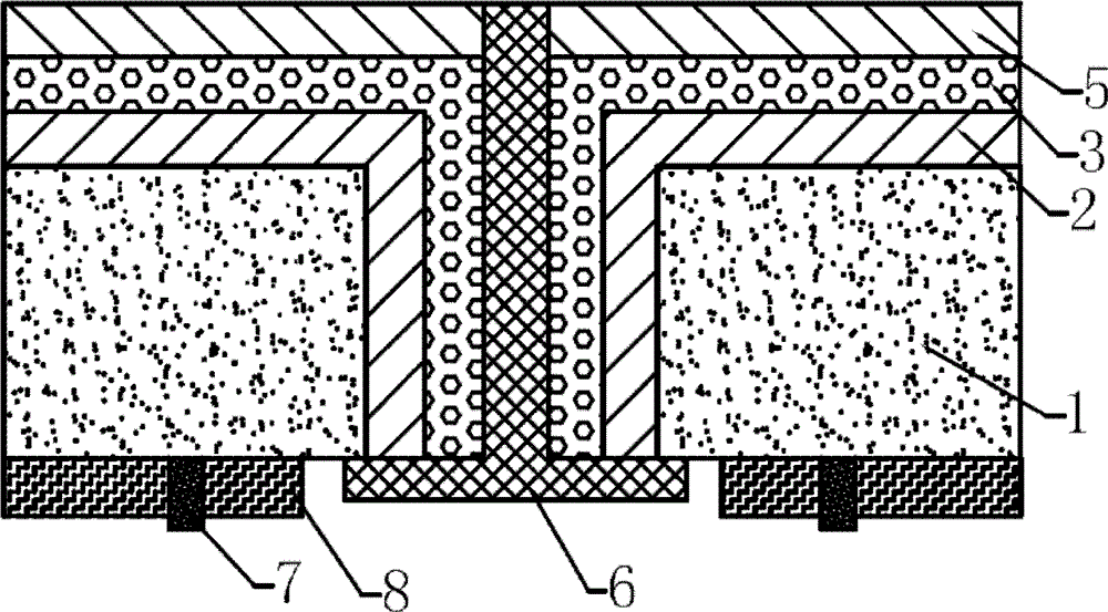
The invention discloses a method for preparing a back-contact silicon solar cell, which comprises the following steps: (1) performing texturing on the light-receiving surface of a silicon wafer, and then opening holes; (2) performing coating source diffusion on the light-receiving surface of the silicon wafer Make a junction, form a PN junction on the light-receiving surface and the hole; (3) set a transparent conductive film on the above-mentioned light-receiving surface and the PN junction in the hole; (5) prepare a through-hole electrode, a back metal electrode, and a back passivation field on the non-coated surface of the above-mentioned silicon wafer to obtain the back-contact silicon solar cell; the through-hole electrode and the transparent The conductive film is in electrical communication. The light-receiving surface of the back-contact silicon solar cell prepared by the invention is not shielded by electrodes, which avoids light-shielding loss and significantly improves the photoelectric conversion efficiency; the number of holes to be opened is also greatly reduced, thereby greatly reducing the fragmentation rate and simplifying the preparation process.
Description
Claims (2)
Priority Applications (1)
| Application Number | Priority Date | Filing Date | Title |
|---|---|---|---|
| CN2011103740324A CN102403406B (en) | 2011-11-22 | 2011-11-22 | Preparation method for back contact type silicon solar cell |
Applications Claiming Priority (1)
| Application Number | Priority Date | Filing Date | Title |
|---|---|---|---|
| CN2011103740324A CN102403406B (en) | 2011-11-22 | 2011-11-22 | Preparation method for back contact type silicon solar cell |
Publications (2)
| Publication Number | Publication Date |
|---|---|
| CN102403406A CN102403406A (en) | 2012-04-04 |
| CN102403406B true CN102403406B (en) | 2013-12-04 |
Family
ID=45885413
Family Applications (1)
| Application Number | Title | Priority Date | Filing Date |
|---|---|---|---|
| CN2011103740324A Active CN102403406B (en) | 2011-11-22 | 2011-11-22 | Preparation method for back contact type silicon solar cell |
Country Status (1)
| Country | Link |
|---|---|
| CN (1) | CN102403406B (en) |
Families Citing this family (3)
| Publication number | Priority date | Publication date | Assignee | Title |
|---|---|---|---|---|
| CN102629641B (en) * | 2012-04-13 | 2014-08-06 | 苏州阿特斯阳光电力科技有限公司 | Preparation method of back contact silicon solar cell |
| CN102683494A (en) * | 2012-05-27 | 2012-09-19 | 苏州阿特斯阳光电力科技有限公司 | Preparation method of double-sided back contact solar cell |
| CN102694069B (en) * | 2012-05-27 | 2015-05-20 | 苏州阿特斯阳光电力科技有限公司 | Method for preparing N-type double-sided back-contact crystalline silicon solar battery |
Citations (4)
| Publication number | Priority date | Publication date | Assignee | Title |
|---|---|---|---|---|
| CN1813356A (en) * | 2003-06-26 | 2006-08-02 | 日出能源公司 | Back contact solar cell with integrated conductive vias and method of manufacture |
| CN101088159A (en) * | 2004-09-07 | 2007-12-12 | 日出能源公司 | Process and fabrication methods for emitter wrap through back contact solar cells |
| CN102132423A (en) * | 2008-08-27 | 2011-07-20 | 应用材料股份有限公司 | Back Contact Solar Module |
| CN102184976A (en) * | 2011-06-10 | 2011-09-14 | 山东力诺太阳能电力股份有限公司 | Back contact heterojunction solar battery |
Family Cites Families (2)
| Publication number | Priority date | Publication date | Assignee | Title |
|---|---|---|---|---|
| TWI415277B (en) * | 2009-11-20 | 2013-11-11 | Ind Tech Res Inst | Solar cell structure |
| NL2004310C2 (en) * | 2010-02-26 | 2011-08-30 | Stichting Energie | Method of fabrication of a back-contacted photovoltaic cell, and back-contacted photovoltaic cell made by such a method. |
-
2011
- 2011-11-22 CN CN2011103740324A patent/CN102403406B/en active Active
Patent Citations (4)
| Publication number | Priority date | Publication date | Assignee | Title |
|---|---|---|---|---|
| CN1813356A (en) * | 2003-06-26 | 2006-08-02 | 日出能源公司 | Back contact solar cell with integrated conductive vias and method of manufacture |
| CN101088159A (en) * | 2004-09-07 | 2007-12-12 | 日出能源公司 | Process and fabrication methods for emitter wrap through back contact solar cells |
| CN102132423A (en) * | 2008-08-27 | 2011-07-20 | 应用材料股份有限公司 | Back Contact Solar Module |
| CN102184976A (en) * | 2011-06-10 | 2011-09-14 | 山东力诺太阳能电力股份有限公司 | Back contact heterojunction solar battery |
Also Published As
| Publication number | Publication date |
|---|---|
| CN102403406A (en) | 2012-04-04 |
Similar Documents
| Publication | Publication Date | Title |
|---|---|---|
| CN102208486B (en) | Preparation method of MWT (Metal Wrap Through) solar cell | |
| CN108807565A (en) | A kind of passivation contact electrode structure, applicable solar cell and production method | |
| CN102623517B (en) | Back contact type crystalline silicon solar cell and production method thereof | |
| JP2021061395A (en) | Solar cell and manufacturing method thereof | |
| CN105789342B (en) | A kind of metal oxide multilayer film back contacts crystal-silicon solar cell and preparation method thereof | |
| CN101651163B (en) | Thin film type solar cell and method for manufacturing the same | |
| CN101882650A (en) | Preparation method of solar cell with charge buried layer | |
| CN102468365A (en) | Method for manufacturing double-sided solar cell | |
| CN208806263U (en) | A kind of passivation contact electrode structure and its applicable solar battery | |
| CN102214719B (en) | Back contact heterojunction solar battery based on N-type silicon slice | |
| CN102332495A (en) | Fabrication method for crystalline silicon solar cell | |
| CN102956723B (en) | A kind of solar cell and preparation method thereof | |
| CN102403369A (en) | Passivation dielectric film for solar cell | |
| CN102386254A (en) | Metal wrap through (MWT) back contact solar cell, preparation method and assembly thereof | |
| CN108666376A (en) | A kind of p-type back contacts solar cell and preparation method thereof | |
| CN114447025A (en) | Laminated perovskite solar cell and manufacturing method thereof | |
| CN102224601A (en) | Method for manufacturing solar cell | |
| CN103904138A (en) | Full back side contact crystalline silicon cell and preparation method thereof | |
| CN102185030A (en) | Preparation method of back contact HIT solar battery based on N-type silicon wafer | |
| CN102214720B (en) | Back contact heterojunction solar battery based on P-type silicon slice | |
| CN102403406B (en) | Preparation method for back contact type silicon solar cell | |
| KR20090075421A (en) | Solar cell | |
| CN108666379A (en) | A kind of p-type back contact solar cell and its preparation method | |
| CN202977438U (en) | Full back contact crystalline silicon cell | |
| CN102403404A (en) | Preparation method for back contact type photovoltaic cell |
Legal Events
| Date | Code | Title | Description |
|---|---|---|---|
| C06 | Publication | ||
| PB01 | Publication | ||
| C10 | Entry into substantive examination | ||
| SE01 | Entry into force of request for substantive examination | ||
| C14 | Grant of patent or utility model | ||
| GR01 | Patent grant | ||
| CP01 | Change in the name or title of a patent holder | ||
| CP01 | Change in the name or title of a patent holder |
Address after: 215129 Suzhou high tech Zone, Jiangsu Province, Lu Shan Road, No. 199, No. Co-patentee after: Artes sunshine Power Group Co. Ltd. Patentee after: Suzhou Canadian Solar Inc. Address before: 215129 Suzhou high tech Zone, Jiangsu Province, Lu Shan Road, No. 199, No. Co-patentee before: Canadian (China) Investment Co., Ltd. Patentee before: Suzhou Canadian Solar Inc. |
|
| CP03 | Change of name, title or address | ||
| CP03 | Change of name, title or address |
Address after: No. 199, deer mountain road, Suzhou high tech Zone, Jiangsu Province Patentee after: CSI Cells Co.,Ltd. Patentee after: Atlas sunshine Power Group Co.,Ltd. Address before: 215129 199 deer Road, Suzhou hi tech Development Zone, Jiangsu, Suzhou Patentee before: CSI Cells Co.,Ltd. Patentee before: CSI SOLAR POWER GROUP Co.,Ltd. |