CN1032233C - Method for photolithographically forming self-aligned mask using back-side exposure and non-specular reflecting layer - Google Patents

Method for photolithographically forming self-aligned mask using back-side exposure and non-specular reflecting layer Download PDF

Info

Publication number
CN1032233C
CN1032233C CN91102566A CN91102566A CN1032233C CN 1032233 C CN1032233 C CN 1032233C CN 91102566 A CN91102566 A CN 91102566A CN 91102566 A CN91102566 A CN 91102566A CN 1032233 C CN1032233 C CN 1032233C
Authority
CN
China
Prior art keywords
layer
photoresist
deposit
preliminary election
exposure
Prior art date
Legal status (The legal status is an assumption and is not a legal conclusion. Google has not performed a legal analysis and makes no representation as to the accuracy of the status listed.)
Expired - Fee Related
Application number
CN91102566A
Other languages
Chinese (zh)
Other versions
CN1056187A (en
Inventor
乔治·爱德华·波辛
西格弗里德·阿夫特格特
Current Assignee (The listed assignees may be inaccurate. Google has not performed a legal analysis and makes no representation or warranty as to the accuracy of the list.)
General Electric Co
Original Assignee
General Electric Co
Priority date (The priority date is an assumption and is not a legal conclusion. Google has not performed a legal analysis and makes no representation as to the accuracy of the date listed.)
Filing date
Publication date
Application filed by General Electric Co filed Critical General Electric Co
Publication of CN1056187A publication Critical patent/CN1056187A/en
Application granted granted Critical
Publication of CN1032233C publication Critical patent/CN1032233C/en
Anticipated expiration legal-status Critical
Expired - Fee Related legal-status Critical Current

Links

Images

Classifications

    • HELECTRICITY
    • H10SEMICONDUCTOR DEVICES; ELECTRIC SOLID-STATE DEVICES NOT OTHERWISE PROVIDED FOR
    • H10DINORGANIC ELECTRIC SEMICONDUCTOR DEVICES
    • H10D30/00Field-effect transistors [FET]
    • H10D30/01Manufacture or treatment
    • H10D30/021Manufacture or treatment of FETs having insulated gates [IGFET]
    • H10D30/031Manufacture or treatment of FETs having insulated gates [IGFET] of thin-film transistors [TFT]
    • H10D30/0312Manufacture or treatment of FETs having insulated gates [IGFET] of thin-film transistors [TFT] characterised by the gate electrodes
    • H10D30/0316Manufacture or treatment of FETs having insulated gates [IGFET] of thin-film transistors [TFT] characterised by the gate electrodes of lateral bottom-gate TFTs comprising only a single gate
    • HELECTRICITY
    • H10SEMICONDUCTOR DEVICES; ELECTRIC SOLID-STATE DEVICES NOT OTHERWISE PROVIDED FOR
    • H10DINORGANIC ELECTRIC SEMICONDUCTOR DEVICES
    • H10D30/00Field-effect transistors [FET]
    • H10D30/01Manufacture or treatment
    • H10D30/021Manufacture or treatment of FETs having insulated gates [IGFET]
    • H10D30/031Manufacture or treatment of FETs having insulated gates [IGFET] of thin-film transistors [TFT]
    • H10D30/0321Manufacture or treatment of FETs having insulated gates [IGFET] of thin-film transistors [TFT] comprising silicon, e.g. amorphous silicon or polysilicon
    • HELECTRICITY
    • H10SEMICONDUCTOR DEVICES; ELECTRIC SOLID-STATE DEVICES NOT OTHERWISE PROVIDED FOR
    • H10PGENERIC PROCESSES OR APPARATUS FOR THE MANUFACTURE OR TREATMENT OF DEVICES COVERED BY CLASS H10
    • H10P76/00Manufacture or treatment of masks on semiconductor bodies, e.g. by lithography or photolithography
    • H10P76/20Manufacture or treatment of masks on semiconductor bodies, e.g. by lithography or photolithography of masks comprising organic materials
    • H10P76/204Manufacture or treatment of masks on semiconductor bodies, e.g. by lithography or photolithography of masks comprising organic materials of organic photoresist masks
    • H10P76/2041Photolithographic processes

Landscapes

  • Thin Film Transistor (AREA)
  • Liquid Crystal (AREA)
  • Photosensitive Polymer And Photoresist Processing (AREA)
  • Exposure And Positioning Against Photoresist Photosensitive Materials (AREA)
  • Exposure Of Semiconductors, Excluding Electron Or Ion Beam Exposure (AREA)

Abstract

一种光刻制造掩模方法包括下列步骤:在透明衬底主表面上形成岛状结构;在该表面和整个岛状结构上淀积至少一透明材料层;在整个至少一透明层上淀积光致抗蚀材料层;将该表面对面的衬底表面背面在紫外光中曝光,将至少一部分紫外光反射回光致抗蚀层中;在紫外曝光之前在光致抗蚀层上淀积非镜面层,然后除去经曝光的光致抗蚀部分,以形成与岛状结构对准且其各边比岛状结构窄一预选重叠距离的掩模。

Figure 91102566

A method for producing a mask by photolithography comprises the following steps: forming an island structure on the main surface of a transparent substrate; depositing at least one transparent material layer on the surface and the entire island structure; depositing a layer of transparent material on the entire at least one transparent layer a layer of photoresist material; exposing the backside of the substrate surface opposite the surface to ultraviolet light, reflecting at least a portion of the ultraviolet light back into the photoresist layer; depositing non- The mirror layer is then removed from the exposed photoresist portions to form a mask that is aligned with the islands and whose sides are narrower than the islands by a preselected overlap distance.

Figure 91102566

Description

Form the method for self-aligned mask with back-exposure and non-mirror reflection layer photoetching
The present invention relates to make the photoetching technique of semiconductor device, more particularly, relate to the photoetching method that a kind of each part that utilizes back-exposure and non-mirror reflection to make the semiconductor body is aimed at.
Whether each part of semiconductor device is correctly aimed at, so this is very important to film field effect transistor (FET) semiconductor device.Make this device reach the service behaviour of Cui, source electrode, drain electrode or both should with the distance of one section preliminary election of gate overlap, preferably about the 1-10 micron.Overlap distance is crossed conference makes source grid and drain-gate (S/D-G) electric capacity become big, thereby transistor noise is increased, and is adopting film F ET can produce hysteresis in as the imaging type body of switch element.The increase of S/D-G electric capacity also may be that the offset voltage error that produces when indivedual pixels switch between work and off position in the LCD (LCD) causes; The electric charge that pixel remains in the S/D-G electric capacity when turn-offing may need to be compensated so that really make this pixel change off position over to.Need with bucking voltage depend on S/D-G electric capacity, and different with the difference of pixel when S/D-G electric capacity changes in a LCD device.
In general, during making, device forms lithography alignment error aequum in the photoresist mask in order to allow, and guaranteeing that an enough big overlapping width is arranged, the S/D-G lap has bigger value under all than above-mentioned two kinds of situations when designing, so that permissible contact or conducting resistance are provided.The overlapping width of S/D-G also may make the saturated drain current of FET fluctuate outside the scope of allowing during less than Cui value.Therefore always wish overlapping between the S/D utmost point and the grid controlled to neither oversize not too short again Cui width.
A very crucial manufacturing step of control S/D-G overlap distance is the formation of scribing the photoresist mask that figure uses on the top layer of FET; For the lap that makes S/D-G reaches optimal distance, mask is answered the Cui width of tool, and should with gate alignment.If the width of mask is too narrow or too wide, perhaps with the grid misalignment, when then scribing the figure of top layer the etching error can appear, and source electrode and drain electrode can and the grid misalignment.
Therefore primary and foremost purpose of the present invention provides a kind of new method of making band autoregistration part and not having the semiconductor device of above-mentioned shortcoming.
Another object of the present invention provides the new method of making the autoregistration thin-film transistor, and this method controls to Cui situation with the overlap distance of source electrode and drain electrode respectively with grid.
Another object of the present invention provides makes the mask that device with autoregistration part is used.
Read the following detailed description book in conjunction with the accompanying drawings and can know that the understanding above and other objects of the present invention are together with characteristics of the present invention.Element same in the accompanying drawing is represented with same numbering.
According to the present invention, in order to make the mask of autoregistration semiconductor device, its manufacture method comprises the following steps: to form island structure with opaque material on the transparent substrates first type surface; Deposit transparent material layer at least on opaque island; Deposit one deck photo-induced corrosion resistant material at least one layer material; Deposit one deck non-specular surface material on photo-induced corrosion resistant material; The back side substrate surface on main substrate surface opposite is exposed in ultraviolet (UV) light, and the length of exposure is selected to such an extent that make photic erosion agent roughly be equivalent at least a portion exposure at the outer position of island structure shade; Make at least a portion ultraviolet light from the reflection of non-specular surface layer, so that another part of photoresist is exposed the selected distance of exposure range in the island structure shade; Remove then through exposure cause the resist part, form aim at island structure and each limit than the mask of the narrow selected overlap distance of island structure.This mask can be used for another material layer of deposit, and the each several part of material layer covers island structure by selected overlap distance, also can be in order to scribe figure at least one layer material.
Figure 1A-1E is a cross sectional side view of making each step that is adopted in the process of mask by photoetching process of the present invention.
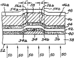
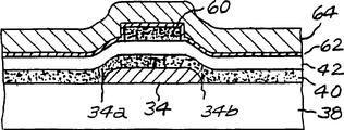
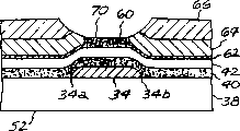
Fig. 2 A-2I uses the cross sectional side view that photoetching process of the present invention is made each step that is adopted in the process of thin-film transistor (TFT).
At first referring to Figure 1A.On the first type surface 12 of the substrate 14 that the insulation transparent material such as glass etc. is made, be formed with the island structure 10 of opaque material.Island structure 10 can be grid or other apparatus assembly that should aim at another device of later formation of field effect transistor (FET).
At least one layer of material 16 in deposit on the entire main surface 12 of island structure 10; For example, when making FET, can be on first type surface 12 and whole grid (island structure 10) go up deposit first insulation material layer 16, can be on ground floor 16 deposit second semiconductor material layer 18.
According to the present invention, shown in Figure 1A, be deposited with positivity photo-induced corrosion resistant material layer 20 on the whole second layer 18, be deposited with non-mirror reflection material layer 22 on the whole photoresist layer 20.In present Cui embodiment, the desirable about 2 microns thickness of photoresist layer.For the interaction of non-crystal face reflecting material and photoresist being reduced to minimum, non-crystal face reflecting material preferably adopts high reflection material or the high dielectric of refractive index that is dispersed in the aqueous solution that contains the polymer such as polyvinyl alcohol, gel etc., for example TiO2, BaSO4 etc.The aqueous solution that wherein is dispersed with reflection grain can be coated on the photoresist layer 22 with whirl coating, spraying process.Ultraviolet (UV) radiation (representing with arrow 24) shines substrate 14 back sides 26 on substrate main surface 12 opposites.Ultraviolet ray sees through substrate 14 and material layer 16 and 18 and makes haply photoresist layer segment 20a exposure corresponding to the outer position (with dashed lines 28a and 28b represent) of island 10 edge 10a, 10b.Non-specular surface layer 22 will incide a part of ultra-violet radiation reflection on the material layer 22 and be scattered back in the photoresist, impel at least one selected distance of photoresist layer 20 in island 10 each edge 10a and 10b and expose.The size of particle should be less than desired space length (be selected apart from d) in the control, to guarantee reverberation scattering equably under the same order of magnitude; For example, the size of particle should be less than 1 micron, to guarantee reverberation evenly scattering under micron order.The shape of non-specular surface layer 22 can impel the major part that makes photoresist press close to the second layer 18 through reflection and the ultraviolet light of scattering to expose, thereby the part 30 (among Figure 1A be boundary with line 31a and 31b) that makes photoresist layer 20 be bowl-type is not haply exposed.Selected is the reflection coefficient of material layer 22, thickness and the duration of uv-exposure and the function of intensity of photoresist layer 20 apart from d.
As represent among Figure 1B that photoresist layer 20 will be removed through the development of photoresist of exposure, stay the photoresist part 30 without exposure after uv-exposure, this part promptly constitutes the mask that uses in the later procedure of processing.For the width that further reduces mask 30 and control selected apart from d, through the photoresist of exposure also can overdevelop except the overexposure that has ultraviolet light or these two excessively alternately occur.Selected can be between about 1 micron and about 10 microns apart from d, and this depends on above-mentioned state-variable.
Non-specular surface layer 22 dissolving such as available water, solvent and it is removed from photoresist layer 20 after the uv-exposure is in case may produce interference problem or operation compatibling problem in the various processes afterwards.
Mask 30 can for example metallize etc. in order to the figure (Fig. 1 C) of scribing material layer 18 and as when not scribing figure on material layer 18 (or thereon) another material layer 32 of deposit on Fig. 1 material layer that D is shown in 16 and the mask 30.When divesting photoresist mask 30, therefore also can remove the part 32 of material layer 32 ', stay the sort of structure shown in Fig. 1 E.The part 32a of material layer 32 and 32b can aim at voluntarily with island 10, and with island 10 overlapping selected at least overlap distance d ', shown in Fig. 1 E.
In this Cui embodiment, can about 20 weight % be dispersed in formation non-mirror reflection layer 22 in 20% gel and the water to the TiO2 powder of about 30 weight %; Then the solution that draws is spun on the photoresist layer 20 to about 1000 rev/mins rotating speed with about 500 rev/mins, lasts between about 8 seconds to 30 seconds, to form the material layer of some micron thickness.At room temperature dry about 2 hours of the most handy air of gel contains at least approximately film of 50%TiO2 particle to make.The also available slight baking process of gel is about 5 minutes of about 90 ℃ or following temperature drying, and heating may destroy contacting between photoresist layer 20 and the non-specular surface layer 22, but the change in size of photoresist layer 20 is little or do not have an obvious variation.
After the uv-exposure, the gel layer of just having mentioned can be removed with warm water or hot water, and with wipings gently such as clean soft cloths, in case may influence the various processes of back; Remove after the gel layer, can be under about room temperature with development of photoresist about 25 seconds.
As another example, the field boundary that method of the present invention can be used for making thin-film transistor (TFT) closes, shown in Fig. 2 A-2I.
Referring to Fig. 2 A, on the first type surface 36 of the substrate 38 that the insulation transparent material such as glass is made, form grid 34 earlier.Grid can be the conducting metal of individual layer, for example titanium (Ti), chromium (Cr), tungsten (W), aluminium (Al) etc., it also can be sandwich construction, for example titanium covers (Ti/Mo) on the molybdenum, titanium covers on the aluminium (Ti/Al), chromium and covers that (Cr/Al), chromium cover (Cr/Mo) or the like on the molybdenum on the aluminium, itself and substrate 14 are bondd well, and resistance is little.The side 34a of grid 34 and the most handy known wet type of 34b or dry corrosion legal system are tapered, and the step of each deposition of materials layer covers so that improve thereafter on whole gate edge.The thickness t of grid 34 is preferably between about 100 millimicrons and about 500 millimicrons.
Among Fig. 2 B, be deposited with on the main substrate surface 36 and on the whole grid 34 about 100 millimicrons to about 600 millimicrons of first thick insulation material layers 40; On first insulation material layer 40 with the semi-conducting material 42 between thick about 20 millimicrons and about 200 millimicrons of known technology (for example the chemical vapor deposition method (PECVD) that strengthens of plasma etc.) the deposit last layer, for example intrinsic amorphous silicon (i-Si), amorphous Germanium (a-Ge) and polycrystalline semiconductor material etc.Second insulating barrier 44 on the semiconductor layer 42 between thick about 100 millimicrons to about 800 millimicrons of the deposit last layer.First and second insulating barriers can be formed with known method (for example PECVD etc.) deposit by one or more layers silicon nitride (SiNx), silica (SiOx), nitric acid silicon (SiNxOy) or other suitable dielectric material.
According to the present invention, shown in Fig. 2 B, on whole second insulating barrier 44, be deposited with positivity photo-induced corrosion resistant material 46, on whole photoresist layer 46, be deposited with non-mirror reflection material layer 48.Material layer 48 can be the above-mentioned particle that is dispersed in high dielectric of high reflection metal, refractive index in the aqueous solution etc.Ultraviolet (UV) radiation (representing with arrow 50) shines on the backside surface 52 of substrate 38 of main substrate surface, and sees through substrate 38 and material layer 40,42 and 44 makes the part 46a exposure of photoresist layer corresponding to gate edge outside left (with dashed lines 54a and 54b represent among Fig. 2 B).Reflector 48 makes a part of ultra-violet radiation scattering get back to photoresist layer 46, impels the photoresist exposure of preselected distance d ' in grid 34 shades.It is that boundary and its close second insulating barrier, 44 places may narrow down with line 56a and 56b that photoresist layer 46 is bowl-shaped portion 58 haply, and this part is not exposed by ultraviolet radiation.Non-mirror reflection layer 48 can be removed after uv-exposure to avoid the various processes after on the technology incompatible.
Shown in Fig. 2 C, photoresist layer 46 after uv-exposure, will through the exposure development of photoresist and remove, stay the photoresist layer segment 58 that is bowl-type basically.Photoresist through exposure removes and may cross the also possibility overdevelop of being outside one's consideration by uv-exposure, and perhaps two kinds excessively alternately occur, so that further reduce the thickness of remaining photoresist part 58, and control selected overlap distance d '.Apart from d ' preferably choose about 1 micron to about 10 microns scope.
Referring now to Fig. 2 D,, those parts that second insulating barrier 44 has not been sheltered for photoresist are now removed with known etching technique.For example, when second insulating barrier 44 is SiNx or SiOx, available buffered hydrofluoric acid (BHF) or hydrofluoric acid (HF) corrosion.According to the present invention, second insulating barrier 44 can excessive corrosion with the bottom of the remaining photoresist part 58 of undercutting, thereby the width of second insulated part 60 that reduces to be left and is further controlled selected overlap distance d '.Then can with the control of following state-variable selected apart from d ': (1) makes the photoresist overexposure; (2) make the photoresist overdevelop; (3) make second insulating barrier, 20 excessive corrosion; (4) reflection coefficient in reflector 48; (5) thickness of photoresist layer 46; These state-variables can be individually or unite be applied control selected apart from d '.Erode after second insulating barrier 44, remove remaining photoresist part 58.
In some applications, for example in X-ray, optics or charged particle imager or liquid crystal display (LCD) device, be preferably in deposit source/drain electrode (S/D) metal layer and scribe the figure of semiconductor layer 42 before, the zone of semi-conducting material under the S/D metal layer being reduced to minimum, and on substrate, reserve additional positions for the element such as pixel capacitors etc.Semiconductor layer 42 can be at this moment in the course of processing or after the semiconductor layer 62 of deposit through mixing (Fig. 2 E) scribe figure, under latter event, two material layers 42 and 62 corrode in same masking steps; Alternative two embodiment of the present invention have introduction in the U.S. Patent application (agent's folder is numbered RD-191588) that is entitled as " method that the autoregistration thin-film transistor is made in using planarization and the exposure of back side photoresist layer ".This patent application also transfers same assignee of the present invention, examines for also it being comprised for the purpose of complete considering for ginseng in this manual.
As if not thinking or need on semiconductor layer 42, not scribing figure, then can go up deposit S/D metal 64 at whole semiconductor layer 62 (Fig. 2 E) through mixing.Doping semiconductor layer 62 is n+ type conductivity preferably, and this available amorphous silicon of mixing phosphorus forms, and its deposition thickness is between about 10 millimicrons to about 200 millimicrons.So material layer 62 forms between S/D metal layer 64 and the semiconductor layer 42 that underlies and contacts.The S/D metal layer can be a contacting metal, and for example molybdenum (MO), chromium (Cr) etc. are deposited to thickness between about 100 millimicrons and about 500 millimicrons with sputtering method or other known method.
Shown in Fig. 2 F, according to another situation of the present invention, be deposited with a planarisation material layer 66 basically on the whole wafer, for example photo-induced corrosion resistant material etc. comprehensively.Use complanation etching method [for example reactive ion etching method (RIE)] to carry out non-selective deep etch then.In originally Cui embodiment,, the top section 68 of S/D metal layer 64 is come out (Fig. 2 G) with dry ecthing method etch planarization layer 66; Then with the complanation layer that is carved with figure as the mask S/D metal layer 64 and the semiconductor doping layer 62 that come out of etch exposed selectively, till the second remaining insulated part 60 comes out (Fig. 2 H).At this moment can divest remaining complanation layer 66 (Fig. 2 I). Etch layer 64 and 62 forms autoregistration source electrode 64a and drain electrode 64b, and both are overlapping grid 34 preselected distance d ' (Fig. 2 I) respectively; Apart from d ' is to choose to such an extent that make S/D-G electric capacity minimum, still forms permissible contact resistance simultaneously.S/D metallization 64 can needle drawing be not shown separately again after the step shown in Fig. 2 I.Perhaps if not metal layer 64 also can carry out needle drawing before at deposit complanation layer 40 (Fig. 2 F), and this application by the FET device need be done like this.
Those skilled in the art that scholar is understood that the present invention is not limited to described here and specific embodiment that exemplified.Except shown in this specification and described, obviously or fully have reason now according to the above description to propose various embodiment and application and unlikely disengaging the spirit and scope of the invention with accompanying drawing.Although the present invention here has been described in detail with regard to its Cui embodiment, it should be understood that the disclosure content only is to illustrate of the present invention, only be in order to disclose content of the present invention all sidedly.Therefore, ours is intended that the restriction that only makes the present invention be subjected to the spirit and the scope of this specification appending claims.

Claims (28)

1. a method of making mask is characterized in that, this method comprises the following steps:
(a) island structure of formation opaque material on the first type surface of transparent substrates;
(b) deposit transparent material layer on main substrate surface and whole island structure;
(c) the photo-induced corrosion resistant material layer of deposit preliminary election thickness at least one material layer;
(d) back side substrate surface with main substrate surface opposite exposes in ultraviolet (UV) light of predetermined strength, lasts predetermined time duration, so that photoresist is corresponded essentially to the part exposure at the outer position of island structure shade;
(e), photoresist layer is exposed apart from the another part in the island structure shade one preliminary election overlap distance with on the photic resist layer of at least a portion ultraviolet (UV) light reflected back.
(f) develop selectively, remove photoresist part, thereby formation island structure aligning and each limit are than the mask of the narrow preliminary election overlap distance of island structure through exposure.
2. the method for claim 1 is characterized in that, step (e) is included in step (d) step of deposit one deck non-specular surface material layer on photoresist layer before.
3. method as claimed in claim, it is characterized in that, step (d) comprises such step: select the duration and the intensity of uv-exposure, make ultraviolet light from the reflection of non-specular surface layer, thereby make the overlap distance that extends to each the side preliminary election of island structure shade through the photoresist layer segment of exposure.
4. method as claimed in claim 2 is characterized in that, described non-specular surface layer depositing step can be selected spin coating step or spraying step.
5. method as claimed in claim 2 is characterized in that, the non-specular surface layer is made up of at least a a large amount of particles in the dielectric that is dispersed in high reflection metal in the polymer solvent and high refractive index.
6. method as claimed in claim 5 is characterized in that, each a large amount of particle is less than the overlap distance of institute's preliminary election.
7. method as claimed in claim 5 is characterized in that, polymeric solution one of comprises at least in the polyvinyl alcohol and gel.
8. method as claimed in claim 5 is characterized in that, described a large amount of particles respectively contain one of them kind of TiO2 and BaSO4.
9. method as claimed in claim 2 is characterized in that, non-specular surface layer depositing step comprises the following steps:
TiO2 is dispersed in the solution of water and gel composition, to form mixed solution;
Apply mixed solution to form the non-specular surface layer with spin-coating method or spraying process; With
Dry non-specular surface layer under the duration of preselected temperature and preliminary election.
10. method as claimed in claim 9 is characterized in that, the TiO2 that described mixed solution comprises between 20 weight % to the 30 weight % is dispersed in the solution of being made up of the gel of water and 20%.
11. method as claimed in claim 9 is characterized in that, selected temperature is between 10 ℃ and 90 ℃, and the selected duration is between 5 minutes to 2 hours.
12. method as claimed in claim 9 is characterized in that, described applying step comprised described mixed solution with the duration between 500 rev/mins to 1000 rev/mins 8 seconds in second to 30 of rotating speed spin coating.
13. method as claimed in claim 2 is characterized in that, described non-specular surface layer comprises at least 50% TiO2 particle.
14. method as claimed in claim 2 is characterized in that, this method in step (d) and (e) also comprises the step of removing the non-specular surface layer afterwards.
15. method as claimed in claim 14 is characterized in that, described step (f) is included in removes the non-specular surface layer afterwards at room temperature to the development of photoresist step in 25 seconds.
16. the method for claim 1 is characterized in that, 2 microns of described photoresist bed thickness.
17. method is characterized in that according to claim 1, step (f) includes the photoresist part overdevelop that selectively makes through exposure, impels the step of each limit of mask than the overlap distance of the short preliminary election of island structure.
18. the method for claim 1 is characterized in that, the described overlap distance of choosing is the function of at least one parameter in following each parameter: the selection thickness in the step (c); Selection intensity in the step (d); The selection duration in the step (d); The selected amount of the ultraviolet light that is reflected in the step (e); And the selection of step (f) is developed.
19. a method of making thin-film transistor is characterized in that this method comprises the following steps:
(a) on the first type surface of transparent substrates, form opaque grid;
(b) deposit first insulation material layer on main substrate surface and whole grid;
(c) deposit semiconductor material layer on first insulating barrier;
(d) deposit second insulation material layer on semiconductor layer;
(e) deposit first photoresist layer on second insulating barrier;
(f) back side substrate surface with main substrate surface opposite exposes in the ultraviolet light of preliminary election intensity, through the duration of preliminary election, makes the exposure of at least a portion outside the grid shade haply of first photoresist layer;
(g) make in the photic resist layer of at least a portion ultraviolet light reflected back, photoresist layer is exposed apart from the another part in the preliminary election overlap distance of grid shade;
(h) remove the first photoresist part of having exposed at least by developing selectively, stay the first remaining photoresist part, and second insulating barrier is not come out for the part that remaining first photoresist part is covered;
(i) the etching second insulating barrier part selectively, stay the residue second photoresist part below the photoresist part that first is left, and semiconductor layer is not come out for the part that the second remaining insulation division branch covers, remaining second insulated part and gate alignment, and the overlap distance of a narrow preliminary election is wanted on its each limit compared with grid;
(j) remove the first remaining photoresist part;
(k) semi-conducting material that mixes at the semiconductor portions that exposes and whole second remaining insulated part deposit one deck;
(l) deposit one conductive material layer on the semi-conducting material that mixes;
(m) etching part conductive layer and a part of doping conductor layer selectively, at least one top surface of the second remaining insulated part is come out, and from forming autoregistration source electrode and drain electrode through etched conductive layer, both respectively with the overlap distance of a preliminary election of gate overlap.
20. method as claimed in claim 19 is characterized in that, step (g) is included in step (f) step of deposit one non-specular surface material layer on whole photoresist layer before.
21. method as claimed in claim 20, it is characterized in that, described step (f) comprises duration and the intensity of selecting uv-exposure, and ultraviolet light from non-mirror reflection, and will partly be extended to each side of island structure shade and reach selected overlap distance through the photoresist of exposure.
22. method as claimed in claim 20 is characterized in that, non-specular surface layer depositing step is spin coating step or spraying step.
23. method as claimed in claim 20 is characterized in that, described non-specular surface layer comprises the high reflection metal that is dispersed in the polywater solution and a large amount of particles of at least a composition in the high index of refraction dielectric.
24. method as claimed in claim 23 is characterized in that, a large amount of particles respectively comprises TiO2 or BaSO4.
25. method as claimed in claim 20 is characterized in that, the non-specular surface layer comprises at least 50% TiO2 particle.
26. method as claimed in claim 19 is characterized in that, described preliminary election overlap distance is the function of one of them parameter of following all parameters: the thickness of grid; The selection intensity of step (f); The selection duration of step (f); The a part of ultraviolet light that is reflected in the step (g); The selectivity of step (h) is developed; And the selective etch of step (i).
27. the described method of claim 19 is characterized in that, selected overlap distance is between 1 micron to 2 microns.
28. method as claimed in claim 19 is characterized in that, step (m) comprises the following steps;
Deposit complanation layer on conductive layer; With
Indiscriminate ground etch planarization layer comes out the top surface of conductive layer part.
CN91102566A 1990-04-17 1991-04-17 Method for photolithographically forming self-aligned mask using back-side exposure and non-specular reflecting layer Expired - Fee Related CN1032233C (en)

Applications Claiming Priority (2)

Application Number Priority Date Filing Date Title
US510,767 1990-04-17
US07/510,767 US5130263A (en) 1990-04-17 1990-04-17 Method for photolithographically forming a selfaligned mask using back-side exposure and a non-specular reflecting layer

Publications (2)

Publication Number Publication Date
CN1056187A CN1056187A (en) 1991-11-13
CN1032233C true CN1032233C (en) 1996-07-03

Family

ID=24032112

Family Applications (1)

Application Number Title Priority Date Filing Date
CN91102566A Expired - Fee Related CN1032233C (en) 1990-04-17 1991-04-17 Method for photolithographically forming self-aligned mask using back-side exposure and non-specular reflecting layer

Country Status (6)

Country Link
US (1) US5130263A (en)
EP (1) EP0453169B1 (en)
JP (1) JP3045804B2 (en)
KR (1) KR0185402B1 (en)
CN (1) CN1032233C (en)
DE (1) DE69114175T2 (en)

Cited By (2)

* Cited by examiner, † Cited by third party
Publication number Priority date Publication date Assignee Title
CN1607648B (en) * 2003-09-29 2010-05-26 英特尔公司 A method to make a weight compensating layer on a substrate, system and product therefor
CN107785309A (en) * 2012-03-08 2018-03-09 三星显示有限公司 Manufacture the method for thin film transistor (TFT), manufacture the method and display base plate of display base plate

Families Citing this family (41)

* Cited by examiner, † Cited by third party
Publication number Priority date Publication date Assignee Title
JP2845303B2 (en) * 1991-08-23 1999-01-13 株式会社 半導体エネルギー研究所 Semiconductor device and manufacturing method thereof
KR940008227B1 (en) * 1991-08-27 1994-09-08 주식회사 금성사 Thin Film Transistor Manufacturing Method
KR940007451B1 (en) * 1991-09-06 1994-08-18 주식회사 금성사 Method of manufacturing thin film transistor
US5480818A (en) * 1992-02-10 1996-01-02 Fujitsu Limited Method for forming a film and method for manufacturing a thin film transistor
GB9206086D0 (en) * 1992-03-20 1992-05-06 Philips Electronics Uk Ltd Manufacturing electronic devices comprising,e.g.tfts and mims
KR950005442B1 (en) * 1992-08-24 1995-05-24 현대전자산업주식회사 Phase shift mask manufacturing method
JPH07506703A (en) * 1993-03-01 1995-07-20 ゼネラル・エレクトリック・カンパニイ Self-aligned thin film transistor constructed using lifting method
KR100263900B1 (en) * 1993-03-04 2000-09-01 윤종용 Mask and manufacturing method thereof
US5384271A (en) * 1993-10-04 1995-01-24 General Electric Company Method for reduction of off-current in thin film transistors
KR970004429B1 (en) * 1993-10-29 1997-03-27 현대전자산업 주식회사 Phase reversal mask and its manufacturing method
KR0128827B1 (en) * 1993-12-31 1998-04-07 김주용 Phase reversal mask manufacturing method
KR970005675B1 (en) * 1994-01-19 1997-04-18 Hyundai Electronics Ind Fabrication method of phase shift mask
KR950026032A (en) * 1994-02-25 1995-09-18 김광호 Method of manufacturing polycrystalline silicon thin film transistor
FR2719416B1 (en) * 1994-04-29 1996-07-05 Thomson Lcd Process for passivation of the sides of a thin-film semiconductor component.
JP3176527B2 (en) * 1995-03-30 2001-06-18 シャープ株式会社 Method for manufacturing semiconductor device
US5612235A (en) * 1995-11-01 1997-03-18 Industrial Technology Research Institute Method of making thin film transistor with light-absorbing layer
JP3516424B2 (en) * 1996-03-10 2004-04-05 株式会社半導体エネルギー研究所 Thin film semiconductor device
US5637519A (en) * 1996-03-21 1997-06-10 Industrial Technology Research Institute Method of fabricating a lightly doped drain thin-film transistor
KR100202236B1 (en) * 1996-04-09 1999-07-01 구자홍 Active matrix panel and its making method
JPH1050607A (en) * 1996-07-31 1998-02-20 Sony Corp Method for manufacturing semiconductor device
KR100569729B1 (en) * 1997-04-07 2006-08-10 삼성전자주식회사 Thin film transistor liquid crystal display device substrate using molybdenum tungsten alloy as the source and drain metal and method for manufacturing same
US6395624B1 (en) 1999-02-22 2002-05-28 International Business Machines Corporation Method for forming implants in semiconductor fabrication
US6184069B1 (en) * 1999-05-24 2001-02-06 Chi Mei Electronics Corp. Fabrication of thin film transistor-liquid crystal display with self-aligned transparent conducting layers
US6790599B1 (en) * 1999-07-15 2004-09-14 Microbionics, Inc. Microfluidic devices and manufacture thereof
GB0021030D0 (en) * 2000-08-26 2000-10-11 Koninkl Philips Electronics Nv A method of forming a bottom-gate thin film transistor
US6642085B1 (en) 2000-11-03 2003-11-04 The Regents Of The University Of California Thin film transistors on plastic substrates with reflective coatings for radiation protection
JP2005173037A (en) * 2003-12-09 2005-06-30 Fujitsu Display Technologies Corp Liquid crystal display device and manufacturing method thereof
US7223641B2 (en) * 2004-03-26 2007-05-29 Semiconductor Energy Laboratory Co., Ltd. Semiconductor device, method for manufacturing the same, liquid crystal television and EL television
KR100701088B1 (en) * 2004-10-26 2007-03-29 비오이 하이디스 테크놀로지 주식회사 Method of manufacturing fringe field switching mode liquid crystal display
TWI272725B (en) * 2005-04-15 2007-02-01 Quanta Display Inc Method of fabricating TFT array substrate and metal layer thereof
KR100685936B1 (en) * 2005-06-27 2007-02-22 엘지.필립스 엘시디 주식회사 IPS mode liquid crystal display device and method of manufacturing the same
US8187480B2 (en) * 2008-11-13 2012-05-29 Seagate Technology, Llc Ultra thin alignment walls for di-block copolymer
JP5960430B2 (en) * 2011-12-23 2016-08-02 株式会社半導体エネルギー研究所 Method for manufacturing semiconductor device
KR101951707B1 (en) * 2012-02-14 2019-02-26 삼성디스플레이 주식회사 Method of planarizing substrate and method of manufacturing thin film transistor using the same
CN103345119B (en) * 2013-07-04 2015-03-25 苏州华博电子科技有限公司 Ground hole-containing ceramic thin film circuit photoetching method
CN105206678A (en) * 2015-10-29 2015-12-30 京东方科技集团股份有限公司 Thin film transistor and array substrate manufacturing method
CN105655257A (en) * 2016-01-13 2016-06-08 深圳市华星光电技术有限公司 Manufacturing method of film transistor structure
CN105895534B (en) * 2016-06-15 2018-10-19 武汉华星光电技术有限公司 The preparation method of thin film transistor (TFT)
CN107221563A (en) * 2017-05-10 2017-09-29 陕西师范大学 A kind of bottom gate self-alignment structure metal oxide thin-film transistor and preparation method thereof
JP2019054150A (en) * 2017-09-15 2019-04-04 東芝メモリ株式会社 Semiconductor device manufacturing method and semiconductor wafer
KR102084493B1 (en) * 2019-02-19 2020-03-05 삼성디스플레이 주식회사 Method of planarizing substrate and method of manufacturing thin film transistor using the same

Family Cites Families (12)

* Cited by examiner, † Cited by third party
Publication number Priority date Publication date Assignee Title
IT1123063B (en) * 1975-10-23 1986-04-30 Ici Ltd FILMS OF SYNTHETIC POLYMERIC MATERIALS
US4332879A (en) * 1978-12-01 1982-06-01 Hughes Aircraft Company Process for depositing a film of controlled composition using a metallo-organic photoresist
DE3128949A1 (en) * 1981-07-22 1983-02-10 Basf Ag, 6700 Ludwigshafen LIGHT-SENSITIVE RECORDING MATERIALS FOR THE PRODUCTION OF SCRUBBING AND SCRATCH-RESISTANT PRINTING MOLDS AND METHOD FOR THE PRODUCTION OF gravure FORMS BY MEANS OF THESE RECORDING MATERIALS
DE3265242D1 (en) * 1981-09-17 1985-09-12 Ciba Geigy Ag Light-sensitive coating agent and its use in protection purposes
US4543320A (en) * 1983-11-08 1985-09-24 Energy Conversion Devices, Inc. Method of making a high performance, small area thin film transistor
JPS60223121A (en) * 1984-04-19 1985-11-07 Matsushita Electric Ind Co Ltd Pattern forming method
JPS60224223A (en) * 1984-04-20 1985-11-08 Nec Corp X-ray exposure method
JPS61279862A (en) * 1985-06-06 1986-12-10 Fuji Photo Film Co Ltd Image forming method
JPH01173650A (en) * 1987-12-26 1989-07-10 Seikosha Co Ltd Manufacture of amorphous silicon thin-film transistor
JPH0634401B2 (en) * 1987-12-29 1994-05-02 株式会社精工舎 Method for etching light-shielding thin film
US4898804A (en) * 1988-03-31 1990-02-06 Cornell Research Foundation Self-aligned, high resolution resonant dielectric lithography
US5010027A (en) * 1990-03-21 1991-04-23 General Electric Company Method for fabricating a self-aligned thin-film transistor utilizing planarization and back-side photoresist exposure

Cited By (2)

* Cited by examiner, † Cited by third party
Publication number Priority date Publication date Assignee Title
CN1607648B (en) * 2003-09-29 2010-05-26 英特尔公司 A method to make a weight compensating layer on a substrate, system and product therefor
CN107785309A (en) * 2012-03-08 2018-03-09 三星显示有限公司 Manufacture the method for thin film transistor (TFT), manufacture the method and display base plate of display base plate

Also Published As

Publication number Publication date
EP0453169B1 (en) 1995-11-02
DE69114175T2 (en) 1996-06-05
DE69114175D1 (en) 1995-12-07
US5130263A (en) 1992-07-14
KR0185402B1 (en) 1999-04-15
JP3045804B2 (en) 2000-05-29
CN1056187A (en) 1991-11-13
EP0453169A3 (en) 1991-12-27
JPH05165053A (en) 1993-06-29
EP0453169A2 (en) 1991-10-23

Similar Documents

Publication Publication Date Title
CN1032233C (en) Method for photolithographically forming self-aligned mask using back-side exposure and non-specular reflecting layer
US4700458A (en) Method of manufacture thin film transistor
US4778773A (en) Method of manufacturing a thin film transistor
TW508828B (en) Thin-film transistors and method for producing the same
TW508830B (en) Thin film transistor structure having four procedures of mask processing and the manufacturing method
US5622814A (en) Method for fabricating active substrate
US6809785B2 (en) Semipermeable liquid crystal display device and manufacturing method thereof
US5045487A (en) Process for producing a thin film field-effect transistor
US5670062A (en) Method for producing tapered lines
US6140668A (en) Silicon structures having an absorption layer
JP3510681B2 (en) Method of manufacturing a thin film transistor assembly
JP2011023740A (en) Method for forming amorphous silicon thin film transistor on surface of substrate
JP2011023741A (en) Array
JPH0523057B2 (en)
US7084430B2 (en) Pixel structure and fabricating method thereof
KR100590750B1 (en) Manufacturing method of thin film transistor substrate for liquid crystal display device
US5693567A (en) Separately etching insulating layer for contacts within array and for peripheral pads
JP2678044B2 (en) Active matrix substrate manufacturing method
US5597747A (en) Method of making inverted thin film transistor using backsick exposure and negative photoresist
JPS61204976A (en) Thin film transistor device and its manufacturing method
JPH10321520A (en) Circuit element manufacturing method
JPS6273669A (en) Method for manufacturing thin film transistor device
KR100603847B1 (en) Liquid crystal display device and liquid crystal display device manufacturing method
JPH04505830A (en) Reliable control of source/drain-gate overlap in self-aligned TFTs using top-hat gate electrode format
JPH08313934A (en) Array substrate, manufacturing method thereof, liquid crystal display device and manufacturing method thereof

Legal Events

Date Code Title Description
C06 Publication
PB01 Publication
C10 Entry into substantive examination
SE01 Entry into force of request for substantive examination
C14 Grant of patent or utility model
GR01 Patent grant
C19 Lapse of patent right due to non-payment of the annual fee
CF01 Termination of patent right due to non-payment of annual fee