CN103299542A - Orthogonal basis function set for ditigal predistorter - Google Patents
Orthogonal basis function set for ditigal predistorter Download PDFInfo
- Publication number
- CN103299542A CN103299542A CN2010800710960A CN201080071096A CN103299542A CN 103299542 A CN103299542 A CN 103299542A CN 2010800710960 A CN2010800710960 A CN 2010800710960A CN 201080071096 A CN201080071096 A CN 201080071096A CN 103299542 A CN103299542 A CN 103299542A
- Authority
- CN
- China
- Prior art keywords
- model
- basis function
- predistorter
- output signals
- input signal
- Prior art date
- Legal status (The legal status is an assumption and is not a legal conclusion. Google has not performed a legal analysis and makes no representation as to the accuracy of the status listed.)
- Granted
Links
Images


Classifications
-
- H—ELECTRICITY
- H03—ELECTRONIC CIRCUITRY
- H03F—AMPLIFIERS
- H03F1/00—Details of amplifiers with only discharge tubes, only semiconductor devices or only unspecified devices as amplifying elements
- H03F1/32—Modifications of amplifiers to reduce non-linear distortion
- H03F1/3241—Modifications of amplifiers to reduce non-linear distortion using predistortion circuits
- H03F1/3247—Modifications of amplifiers to reduce non-linear distortion using predistortion circuits using feedback acting on predistortion circuits
-
- H—ELECTRICITY
- H03—ELECTRONIC CIRCUITRY
- H03F—AMPLIFIERS
- H03F1/00—Details of amplifiers with only discharge tubes, only semiconductor devices or only unspecified devices as amplifying elements
- H03F1/32—Modifications of amplifiers to reduce non-linear distortion
- H03F1/3241—Modifications of amplifiers to reduce non-linear distortion using predistortion circuits
- H03F1/3252—Modifications of amplifiers to reduce non-linear distortion using predistortion circuits using multiple parallel paths between input and output
-
- H—ELECTRICITY
- H03—ELECTRONIC CIRCUITRY
- H03F—AMPLIFIERS
- H03F1/00—Details of amplifiers with only discharge tubes, only semiconductor devices or only unspecified devices as amplifying elements
- H03F1/32—Modifications of amplifiers to reduce non-linear distortion
- H03F1/3241—Modifications of amplifiers to reduce non-linear distortion using predistortion circuits
- H03F1/3258—Modifications of amplifiers to reduce non-linear distortion using predistortion circuits based on polynomial terms
-
- H—ELECTRICITY
- H03—ELECTRONIC CIRCUITRY
- H03F—AMPLIFIERS
- H03F3/00—Amplifiers with only discharge tubes or only semiconductor devices as amplifying elements
- H03F3/189—High-frequency amplifiers, e.g. radio frequency amplifiers
- H03F3/19—High-frequency amplifiers, e.g. radio frequency amplifiers with semiconductor devices only
-
- H—ELECTRICITY
- H03—ELECTRONIC CIRCUITRY
- H03F—AMPLIFIERS
- H03F3/00—Amplifiers with only discharge tubes or only semiconductor devices as amplifying elements
- H03F3/20—Power amplifiers, e.g. Class B amplifiers, Class C amplifiers
- H03F3/24—Power amplifiers, e.g. Class B amplifiers, Class C amplifiers of transmitter output stages
-
- H—ELECTRICITY
- H03—ELECTRONIC CIRCUITRY
- H03F—AMPLIFIERS
- H03F2201/00—Indexing scheme relating to details of amplifiers with only discharge tubes, only semiconductor devices or only unspecified devices as amplifying elements covered by H03F1/00
- H03F2201/32—Indexing scheme relating to modifications of amplifiers to reduce non-linear distortion
- H03F2201/3209—Indexing scheme relating to modifications of amplifiers to reduce non-linear distortion the amplifier comprising means for compensating memory effects
Landscapes
- Engineering & Computer Science (AREA)
- Power Engineering (AREA)
- Physics & Mathematics (AREA)
- Nonlinear Science (AREA)
- Algebra (AREA)
- General Physics & Mathematics (AREA)
- Mathematical Analysis (AREA)
- Mathematical Optimization (AREA)
- Pure & Applied Mathematics (AREA)
- Amplifiers (AREA)
Abstract
A predistorter applies a distortion function to an input signal to predistort the input signal. The output of the distortion function is modeled as the sum of the output signals from the orthogonal basis functions weighted by corresponding weighting coefficients. Techniques are described for orthogonalizing the basis function output signals depending on the distribution of the input signal.
Description
Background
The present invention relates generally to techniques for constructing physical models of non-linear electronic devices, and more particularly, to methods and apparatus for compensating for distortions of input signals caused by electronic devices to the input signals.
The design of radio frequency power amplifiers for communication applications often involves a trade-off between linearity and efficiency. Power amplifiers are typically most efficient when operated at or near the saturation point. However, the response of the amplifier at or near the saturation point is non-linear. In general, the response of a power amplifier exhibits non-linearity and memory effects when operating in the high efficiency range.
One way to improve the efficiency of a power amplifier and its overall linearity is to digitally pre-distort the input to the power amplifier to compensate for the distortion caused by the power amplifier. In practice, the input signal is adjusted in anticipation of the distortion caused by the power amplifier, so that the output signal is largely free of distortion products. Usually, the predistortion is applied to the signal digitally at baseband frequency, i.e., before the signal is up-converted to radio frequency.
These techniques can be quite beneficial for improving the overall performance of the transmitter system in terms of both linearity and efficiency. Furthermore, these techniques can be less expensive due to the digital implementation of the predistorter. Indeed, due to the availability of these techniques, the power amplifier may be designed according to more relaxed linearity requirements that would otherwise be allowable, thereby potentially reducing the cost of the overall system.
Disclosure of Invention
The present invention provides a model of a set of orthogonal basis functions for use in a predistortion system. The predistorter applies a distortion function to the input signal to predistort the input signal. The distortion function is modeled by a set of orthogonal basis functions. More specifically, the output of the predistorter is modeled as the sum of the output signals from the orthogonal basis functions weighted by corresponding weighting coefficients. Techniques for orthogonalizing basis function output signals according to a distribution of input signals are described.
In some exemplary embodiments, a method for compensating for distortion of an input signal caused by an electronic device operating on the input signal to generate an output signal is provided. In one exemplary method, a set of model coefficients is computed from a two-dimensional lattice prediction model having a set of input signal samples as a set of basis functions over a predetermined sampling interval. The lattice prediction model represents the basis functions in the set of predistorter basis functions as different combinations of power basis functions. A corresponding set of predistorter connection coefficients is determined from the model coefficients for combining the power basis function output signals to generate the basis function output signals. A set of power basis function output signals is computed from the input signal and the set of power basis functions. The set of predistorter connection coefficients are applied to the power basis function output signals to produce a set of basis function output signals, and the basis function output signals are combined to produce a predistorted input signal from the input signal.
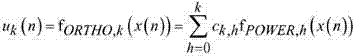
In other embodiments of the present invention, a predistorter circuit is provided for compensating for distortion of an input signal caused by electronics operating on the input signal to generate an output signal. An exemplary predistorter circuit includes a basis function modeling circuit and a predistorter. The basis function modeling circuit computes a set of model coefficients from a set of input signal samples as a two-dimensional lattice prediction model of a set of basis functions over a predetermined sampling interval. The lattice prediction model represents the basis functions in the set of predistorter basis functions as different combinations of power basis functions in the set of power basis functions. Subsequently, a basis function modeling circuit determines a corresponding set of predistorter connection coefficients from the set of model coefficients to combine power basis function output signals from the power basis functions to generate an orthogonalized basis function output signal. The model coefficients calculated by the basis function modeling circuit are used to configure the predistorter. A predistorter computes a set of power basis function output signals from an input signal and the set of power basis functions. The predistorter then applies the set of predistorter connection coefficients to the power basis function output signals to generate a set of basis function output signals, and combines the basis function output signals to generate a predistorted input signal from the input signal.
In an embodiment of the invention, the set of orthogonal basis functions is determined based on the actual input signal. Thus, the resulting set of orthogonal basis functions is customized to fit the distribution of the input signal. With the proposed set of orthogonal basis functions, the data signals derived from the set of orthogonal basis functions can be used to construct a good state matrix, which is beneficial for evaluating the predistorter weighting coefficients.
Drawings
Fig. 1 shows an indirect model for a predistortion circuit.
Fig. 2 shows an indirect model for a predistortion circuit.
Fig. 3 illustrates a conventional distortion model for modeling distortion caused by a predistorter or power amplifier.
Fig. 4 shows a memoryless distortion model for modeling distortion caused by a predistorter or power amplifier.
FIG. 5 illustrates an exemplary set of power basis functions for a distortion model.
FIG. 6 illustrates an exemplary set of power basis functions for a distortion model.
Fig. 7 shows a distortion model with memory for modeling distortion caused by a predistorter or power amplifier.
Fig. 8 illustrates an exemplary orthogonal basis function generator.
Fig. 9 shows the structure of a root node for an orthogonal basis function generator.
Fig. 10 shows a connection node for an orthogonal basis function generator.
Fig. 11 illustrates an exemplary method of pre-distorting an input signal to a power amplifier.
Fig. 12 illustrates an exemplary predistortion circuit for predistorting an input signal to a power amplifier.
Detailed Description
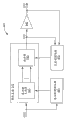
Referring now to the figures, fig. 1 illustrates a digital predistortion system 100 configured to compensate for distortion caused to a communication signal by a power amplifier 120. The power amplifier 120 is generally most efficient when operating in a non-linear range. However, the non-linear response of the power amplifier 120 causes out-of-band emissions and reduces spectral efficiency in the communication system. Predistorter 110 may be used to improve power amplifier efficiency and linearity by distorting the input signal to power amplifier 120 to compensate for nonlinear distortion caused by power amplifier 120. The cascade of predistorter 110 and power amplifier 120 improves the linearity of the output signal and thus allows power amplifier 120 to operate more efficiently. Although predistortion is used in the circuits and systems described herein to linearize the output of the power amplifier 120, those skilled in the art will appreciate that the techniques are more generally applicable to linearizing the output of any type of nonlinear electronic device.
As shown in fig. 1, an input signalx(n) Is input to predistorter 110. Predistorter 110 adapts an input signalx(n) Predistortion to compensate for distortion caused by the power amplifier 120 when the power amplifier 120 is operated in a non-linear range. Predistorted input signal generated by predistorter 110z(n) And then applied to the input of the power amplifier 120. The power amplifier 120 pre-distorts the input signalz(n) Amplifying to generate an output signaly(n). If predistorter 110 is properly designed and configured, the output signaly(n) Containing fewer distortion products and out-of-band emissions than when the power amplifier 120 is used alone.
To compensate for the distortion caused by the power amplifier 120, the predistorter 110 must have a nonlinear transfer function that effectively inverts the nonlinear effects of the power amplifier 120. To properly configure predistorter 110, an appropriate model for this nonlinear transfer function is required. Two different schemes are possible to derive this nonlinear transfer function. The first scheme utilizes an indirect learning architecture as shown in fig. 1, and the second scheme uses the direct learning architecture of fig. 2. In both cases, the signal input to the power amplifier 120z(n) And amplifier output signaly(n) The scaled versions of (a) are applied to the distortion modeling circuit 130. The scaling shown in fig. 1 and 2 as attenuator 140 reflects the net linear gain required from the combination of predistorter 110 and power amplifier 120G. Push buttonGInverse-scaled output signal ofy(n) Allowing the analysis of the non-linearity caused by the power amplifier 120 to be made independent of its gain.
In the indirect learning architecture of fig. 1, the general structure of the model for the predistorter 110 is taken as an assumption, and its coefficients are estimated directly from the input and output of the power amplifier 120 (see fig. 1)Number). The distortion modeling circuit 130 includes a coefficient evaluation circuit 160 to evaluate the amplifier input signal according to a predetermined non-linear model for the predistorterz(n) And amplifier output signaly(n)/GTo determine a set of weighting coefficients to be applied by predistorter 110. This process is described in further detail below. With this indirect scheme, no model is derived for the power amplifier 120. Instead, the non-linear characteristics of the power amplifier 120 are indirectly learned through modeling of the predistortion necessary to cancel the distortion caused by the power amplifier 120.
In contrast, the direct learning architecture of fig. 2 directly characterizes the nonlinear performance of the power amplifier 120. The power amplifier comprises evaluating the amplifier input signal according to a predetermined non-linear model for the power amplifier 120z(n) And the power amplifier output signaly(n)/GThe coefficient evaluation circuit 160. The weighting coefficients that best fit the non-linear characteristics of the power amplifier to the power amplifier model in block 120 are then used by coefficient derivation circuit 170 to generate the weights for configuring predistorter 110.
The distortion caused by predistorter 110 or power amplifier 120 can be represented by a complex nonlinear function, which will be referred to herein as a distortion function. One approach to modeling the distortion function, referred to herein as a decomposition approach, is to decompose the distortion function into a set of less complex basis functions and calculate the output of the distortion function as a weighted sum of the basis function outputs. The set of basis functions used to model the distortion function is referred to herein as a set of basis functions.
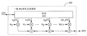
Fig. 3 illustrates a generalized distortion model 200, which may represent the distortion caused by the predistortion transfer function of the power amplifier 120 (e.g., as modeled by the model coefficient evaluation unit 160 in the direct learning architecture of fig. 2) or the predistorter (e.g., as modeled by the predistorter model coefficient evaluation unit 160 of fig. 1). In either case, the distortion model 200 includes a structure 210 corresponding to the desired set of basis functions. The model structure 210 includesPA plurality of taps, wherein eachEach tap corresponds to a basis function. It should be noted that in some embodiments, multiple taps may correspond to the same basis function. Model structure 210 at the input signalx(n) Operate to generate data signals at respective taps. Distortion model 200 then computes the data signal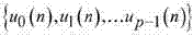 To obtain a distorted input signald(n). More specifically, a data signal
 Multiplying by corresponding weighting coefficients
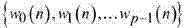 And the resulting products are added together to obtaind(n)。
The distortion model shown in fig. 3 can be expressed as:

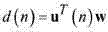
Wherein,uis at time ofnOf data signals output by the model structure Vector, andwbeing weighting coefficients applied to respective data signals
 And (5) vector quantity.
For a given vectoru,d(n) Is the desired output of the distortion model 200. In the direct-learning architecture, the user can,d(n) Is the actual output of the power amplifier 120. In the indirect learning architecture, in order to learn,d(n) Is the desired output of predistorter 110. By fittinguMultiple observations of and corresponding desired outputsd(n) It can be understood that a vector is made during a certain time perioduAnd the required outputd(n) Weighting coefficients for best fitw. For inNThe set of observations within a sampling instant can be represented by the corresponding linear equation given in fig. 2 as:

Wherein,Uis a data signal A matrix, anddis that
 Vector corresponding toNA desired output signal of the distortion model at each of the sampling instants. Matrix arrayUThe columns of (b) correspond to the data signals output by the respective taps, and the rows correspond to different sampling instants.
 Equation 3 can be evaluated according to well-known techniques (e.g., to minimize a criterion such as a least squares error criterion) to find weights that best model the distortion of amplifier 120 or predistorter 110w。
FIG. 4 shows a schematic diagram for amplifying powerAn exemplary memoryless distortion model 300 for modeling a non-linear system such as a predistorter or predistorter. The distortion model 300 includesKA plurality of branches 310, each branch corresponding to a set of basis functionsKOne of the basis functions 320. For convenience, the firstkEach branch 310 corresponds to the second branchkThe order basis function. Input signal samplesx(n) Through each branch 310 and operated on by basis functions 320 to generate data samplesu k (n) The data samples may also be more specifically referred to in this model as basis function output signals. For each input signal samplex(n) Branch 310 generates a basis function output signalu k (n) A corresponding set of. For the first timekThe basis function output signal of each branch 310u k (n) Can be expressed as:
Wherein,is shown askA (the k-th order) basis function. It can be noted that the model has no memory, and therefore, the basis function output signalu k (n) Dependent only on current input samplesx(n). Output signal of basis function Multiplying by corresponding weighting coefficients
 And adding the resulting products to obtain a distorted input signald(n)。
Comparing the memoryless distortion model 300 of FIG. 4 with the general distortion model 200 of FIG. 3, it can be noted that the number of branches in the memoryless distortion model 300KEqual to the number of taps in the general distortion model 200P. It may also be noted that the sampling instants are given in the memoryless model 300nInternal output basis function output signal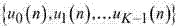 Corresponding to data samples in the
 general distortion model 200 . The model of fig. 4 can therefore be viewed as a special case of the
 distortion model 200 of fig. 3, wherein,K = P。
in thatx(n) Andd(n) Under known conditions, the distortion modeling circuit 130, using the distortion model shown in FIG. 4, calculates the output signal for the basis functionu k (n) Weighting coefficient ofw k (n). Accordingly, the weights that best model the distortion of the amplifier 120 or predistorter 110 can be found in a manner similar to that described abovewE.g. by fitting the output of a set of basis functionsNSub-observed matrix and desired output signal vectord. Since the distortion model 300 does not account for memory effects, the accuracy of this model may be limited with respect to the actual distortion function of a given power amplifier 120.
The set of basis functions used to model the distortion function may comprise a set of power functions used in a polynomial model. FIG. 5 illustrates a structure 400 that may be used to implement a set of power basis functions. The architecture 400 may be implemented in hardware or by processing circuitry. The basis function structure 400 is represented by Is/are as followsKA power basis function, wherein the subscriptkIndication ofkPower of order basis functions, and corresponds to those in the distortion model 400KOne of the branches. Input signal samplesx(n) By each power basis function
 . For each input signal sample, a power basis functionNumber-generating power basis function output signal
 A corresponding set of. Using power basis functions, data samples can be sampledu k (n) Expressed as:

The power basis function output signals are then weighted and added as previously described to generate the output signal of the distortion modeld(n)。
The set of basis functions may be based on the Voltaire series design widely used to model nonlinear systems. In practical applications, a somewhat simplified model containing fewer terms than the full Voltaire series can be used to reduce computational complexity without a large impact on performance. For example, the polynomial model may be obtained by ignoring only power terms, and may be implemented as a multi-branch model, where power functions are used as basis functions and assigned to respective branches 410 of the basis function structure 400.
In some embodiments, the set of orthogonal basis functions may be derived as a sum of power basis function output signals weighted by corresponding scaling coefficients. In this case, the data sample output by the basis function set can be represented as:
Wherein, is shown askOrder orthogonal basis function, term
 Is applied tohA power of order basis function to generatekOrder orthogonal basis function
 The weighting factor of (2). The set of orthogonal basis functions can be advantageous in many applications because it can provide better numerical stability during matrix mathematics for evaluating the weighting coefficients of the distortion model. The set of orthogonal basis functions can be constructed as a weighted addition of power basis functions. The set of orthogonal basis functions can be advantageous in many applications because it can provide better numerical stability during matrix mathematics for evaluating the weighting coefficients of the distortion model.
Fig. 6 illustrates an exemplary basis function generator 500 implementing an orthogonal set of basis functions. The basis function generator 500 may be implemented in hardware or by processing circuitry. Basis function generator 500 includes a series of root nodes 510 and a connection network 520 including a plurality of connection nodes 530. Each root node 510 implements a corresponding power basis function. There is a one-to-one correspondence between the root node 510 and the power basis function. Input signalx(n) A corresponding power basis function output signal is generated by each root node 510 and the power basis function for each root node 510 . The power basis function output signal forms an input signal to the
 connection network 520.
A connection node 530 of the connection network 520 receives an input and generates an output. For convenience, the connection Node 530 of the basis function generator 500 is solely formed by the Node k,h Represent, wherein, indexhIndicating the corresponding power basis function, and indexingkIndicating the corresponding orthogonal basis functions. To Node k,h Is forhThe output of the power basis function of the root node 510. Each connection node 530 multiplies the input by a corresponding weighting factor, referred to herein as a connection coefficient . Then is turned onkIs greater
 thanhFor connecting node 530 in the case of (2), connecting node 530 will beThe weighted power basis function output signals are added. Each row of the connecting network 520 corresponds to an orthogonal basis function. The output of the last (rightmost) connected node 530 in each row comprises an output signal from one of the orthogonal power basis functions 。
。
The set of orthogonal basis functions can be designed based on various criteria. One design that performs well for several common input signal distributions is found in "Orthogonal polynomials for power amplifier modeling and predistorter design," IEEE Transactions on vehicle Technology, vol. 53, No. 5, pp.1468-1479, Sept. 2004, "by Raviv Raich, Hua Qian, and G. Tong Zhou.
Memory effects, i.e. output signals depending on the previous state and the current state of the input signal, can also be included in the distortion function. Fig. 7 illustrates a nonlinear distortion model with memory 600. The distortion model 600 includesKAnd a branch 610. Each branch 610 includes a basis function 620 followed by a corresponding memory model 630. The basis function 620 may be one of a power basis function or an orthogonal basis function as previously described. In this model 600, the memory effect corresponding to each basis function is modeled as havingQA tapped delay line of a number of taps, wherein,Qis the memory length of the memory model 630. Those skilled in the art will appreciate that other memory models, such as lattice predictor memory models, can also be used. The output signal of each branch 610 is at a time including the sum of the current sample timeQ1 previous sampling instantQA weighted sum of the basis function output signals generated for the corresponding basis functions within a sampling instant. For example if used for branchingkHas a basis function of And the input signal isx(n) Then branch offkIs outputted by
 、
、 、
、 And so on. Data signal output from a memory model tap at time n
 Multiplying by corresponding weighting coefficientsAnd the resulting products are added to produce k branch output signals. Then, will come fromKOf a branch 610KThe outputs are added to form a desired distortion signald(n)。
Comparing the distortion model 600 of fig. 7 with the general model 200 of fig. 3, it should be noted that each branch 610 hasQOne tap and have in commonKQA tap andKQa corresponding weight. In this model, the total number of tapsKQEqual to the number of taps in the general model 200P. It should also be noted that it is possible to,KQa data signal Corresponding to the output of the model structure 210 in the general model 200PIndividual data sample
 。
。
In thatx(n) Andd(n) Under known conditions, the distortion modeling circuit 130 using the distortion model 400 shown in FIG. 5 is used to calculate weighting coefficients for the memory model taps . Thus, by recordingKQOf the output of one sampleNSecondary observation to form a matrixUAnd fitting the matrix according to
 equation 3 and a specific optimization criterionUAnd the required outputOutput signal vectordAgain, the weights can be estimatedw(in this case, it is Vector). With the appropriate set of basis functions and memory models of sufficient depth, the resulting distortion will generally provide a better model of real world device distortion than would be provided by a memory-less model.
As suggested in the discussion above, each model in FIGS. 3-7 includes a set of data samples u that can be represented as follows:
This applies regardless of whether the model includes memory. In the case of the memory-less model,is composed of only basis function output signals, i.e. each element is entirely ofx(n) As a function of (c). In the model with the memory, the model is provided with a memory, also included are elements corresponding to the delayed versions of the basis function output signals. Therefore, the temperature of the molten metal is controlled,some of the elements of (1) may correspond tox(n-1)、x(n-2) and the like. Note that in equation 7 and as generally used herein,
 the transpose is represented by,
 which represents the transpose of the conjugate,Pis the number of coefficients in the model,
 vector quantityu(n) Indicating an index at a given timenAll of the data samples in the model are,
 the vector w represents all coefficients in the distortion model, and(n) Is for the time of daynThe desired output of the model.
Index for any given timen,u(n) Andd(n) Are known and equation 7 iswIs given as a linear equation of (a). As described earlier, forNFrom the observations obtained on the time index, the corresponding linear equation represented in equation 7 can be succinctly expressed as:
In the case of the equation 8,Uis a matrix of the input data and,dis the desired output vector.
In the indirect learning architecture of figure 1,d(n) Is the desired output of predistorter 110, ideally with a distortion function that perfectly compensates for the distortion caused by power amplifier 120. Thus, when using an indirect learning architecture,d(n) Correspond toz(n) To the input of the power amplifier 120. The input signals to the distortion model are represented in FIGS. 3-7 asx(n) Corresponding to the scaled output of the power amplifier 120y(n)/G. Thus, for any given model structure, areNEach of the sampling instants takes a sample of the output from the power amplifier 120 and applies it to a set of basis functions to produce a matrixU. This matrix is expressed according to equation 8UAnd the required output vectordFitting, wherein,dis used for forming a matrixUAre the same asNThe work obtained at a sampling timeA vector of samples of the input of the rate amplifier.
As discussed earlier, the distortion characteristics for the power amplifier 120 are modeled directly in the direct learning architecture shown in fig. 2. In this case, the "desired" distortion signald(n) Scaled output corresponding to power amplifier 120y(n)/G. Input to the modelx(n) Corresponding to the input signal of the power amplifier. Thus, for any given model structure, areNEach of the sampling instants takes a sample of the input from the power amplifier 120 and applies it to a set of basis functions to produce a matrixU. This matrix is expressed according to equation 8UAnd the required output vectordFitting, wherein,dis used for forming a matrixUAre the same asNA vector of samples taken at each sampling instant from the scaled output of the power amplifier.
Regardless of the details of the model structure, and regardless of whether an indirect learning architecture or a direct learning architecture is used, the coefficient vector is estimated based on equation 8 satisfying some criterionwIs at the center of the coefficient evaluation of the digital predistorter 110 of fig. 1 and 2. To solve this estimation problem, it is required to use some form of data matrixUInverse of . A well-known measure of the sensitivity of a matrix to digital operations, such as matrix inversion, is the so-called condition number, which is defined as the ratio of the maximum eigenvalue of the matrix to its minimum eigenvalue. A matrix with a condition number close to 1 can be said to be good.
Since the matrix calculation can be quite complex, in the design of the distortion model for the power amplifier 120 or the predistorter 110, an important objective is to provide the coefficient evaluation algorithm with a smaller number of columns (to reduce the computational complexity of the matrix operation), with a condition number as close to 1 as possible (high numerical stability) and, if there are specific optimization criteria, also at the same time as exact as possible the physical behavior of the power amplifier or the predistorterModeled data matrix . The difference between the distribution of the input signal used to derive the set of basis functions for the distortion model and the distribution of the actual data applied to predistorter 110 may result in a data matrix with a large condition number。
This increased instability is reflected in a significant increase in the condition number of the data matrix to be reversed during the coefficient evaluation, sometimes up to 106And (4) doubling. In adaptive digital predistortion systems with memory, this problem can be quite severe because the parameters in such systems are to be adapted "quickly" to track the distortion characteristics of the power amplifier over time. One factor affecting these high condition numbers is the mismatch between the signal distribution of the real-world signal and the signal distribution of the signal used to derive the set of orthogonal basis functions. Thus, the set of orthogonal basis functions formed in view of a particular expected input signal distribution cannot provide an orthogonalized basis function output from a direct application to the actual signal.
Fig. 8 illustrates an orthogonal basis function generator 700 for implementing an orthogonal basis function set. As described in more detail below, the orthogonal basis function generator 700 can be used to generate a set of orthogonalized basis function output signals based on the distribution of the input signals. Thus, a matrix formed from the basis function output signals Will have a matrix ofA low condition number more suitable for coefficient evaluation.
Orthogonal basis function generator 700 includes a plurality of root nodes 710 and a connection network 720 including a plurality of connection nodes 730. Nodes 710, 730 of orthogonal basis function generator 700 are represented by notation Node k,h Represent, wherein, indexkAndhthe rows and columns in fig. 8 are shown. Assume that the input to orthogonal basis function generator 700 isNA finite sequence of input signal samples rather than a continuous stream. Since the input to the orthogonal basis function generator 700 is a finite sequence, a two-dimensional lattice structure is used to orthogonalize the basis function output signals, as described below.
Each node 710, 730 in the orthogonal basis function generator 700 is for each sample time instantnGenerate the respective data of And
And the forward and backward prediction errors of the representation. Then, forward and backward prediction errors are combined
 Andnormalized to generate a respective
 And
And normalized forward and backward prediction error of representation. Normalizing the forward prediction error with respect to the
 root node 710 Equal to normalized backward prediction error
 . As will be described in more detail below, the only input to the
 root node 710 during a sampling instant is a single input signal samplex(n). Identical input signal samplesx(n) Is applied to each root node 710. The connection nodes 730 each have two inputs, these inputs being from Normalized forward prediction error of
 And from
 Normalized backward prediction error of
 . From
 Normalized backward prediction error of
 The
The nodes 710 and 730 shown in the rightmost column of FIG. 8 are the second nodes that can be shown as followskOutput of the order orthogonal basis function:

It should be noted that the output of the orthogonal basis function given in equation 9 is simply the current input samplex(n) And does not depend on previous or future input signal samples.
Fig. 9 shows the structure of the root node 710. Root node 710 is represented by a token Representing nodes where k is equal to 0.
 Root nodes 710 each include a respective power basis function 740 and normalization circuitry 750. The power basis function 740 in each root node 710 is at the input signal samplex(n) Operates to generate forward and backward prediction errors for the root node 710. That is, the forward and backward prediction errors for the root node 710 And
And equal to power basis function output signal
 . Normalization circuit 750 outputs a power basis function signal
 Normalized to a predetermined value to generate normalized forward and backward prediction errors for the
 root node 710 And. More specifically, the normalization circuit 750 outputs the power basis function output signal
 By corresponding normalization factors
 To generate normalized forward and backward prediction errors that can be expressed as follows
 And
And :
:


As will be described below, each root node 710 applies a normalization factorIs an input signal within a predetermined time periodx(n) Variance of (c) and power basis function.
Fig. 10 shows the structure of a connection node 730 of the connection network 720. Each connection node 730 in the connection network 720 includes a lattice update circuit 760 and a normalization circuit 770. As previously described, inputs to a given connection node 730 include inputs from Normalized forward prediction error of
 And fromNormalized backward prediction error of
 . The outputs of the
 connection node 730 are respectively composed of And
And the modified estimates of the normalized forward and backward prediction errors are shown. Just along
 For diagonal nodes, no normalized forward prediction error is used
 And therefore the associated circuitry can be omitted.
The dot matrix update circuit 760 according to the corresponding reflection coefficient Normalized forward and backward prediction errors scaled to
 connected node 730 And
And . More specifically, the forward prediction error to the connecting
 node 730 Multiplying by the reflection coefficientAnd the result product is integrated with the backward prediction error
 Adding to generate a modified backward prediction error
 . Similarly, the backward prediction error input to the
 connection node 730 Multiplied by as
 And the product of the result and the forward predicted error code
 Adding to generate a new forward prediction error
 . For the convenience of this application, the reflection coefficient
 And conjugation thereof
 Considered as the linking coefficients for the lattice predictor model. The corrected forward and backward prediction errors are expressed as:
Equation 13
Normalization circuit 770 corrects the forward and backward prediction errors And
And by corresponding normalization factors
 To generate new normalized forward and backward prediction errors that can be expressed as
 And
And :
:

Normalization of the nodes 710, 730 is introduced to enforce generalized smoothing. Node for given Node k,h Whereinand is andnormalized factor Expressed as:
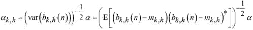
Where term var represents the variance, termERepresenting expected values, and itemsm k,h Representing backward prediction error And at the input signal, andx(n) And equal to 0 with a mean value of 0. It has been noted previously that the backward prediction error is equal to the power basis function output signal in terms of the root node. The term α is the desired square root of the variation and is generally static. For most applications, the required variance can be set equal to 1 for good performance.
Based onNInput sequence of samplesEvaluating reflection coefficients applied by connecting node 730 And
And . Reflection coefficient for connection node 630
 (wherein,
 ) Is represented as follows:
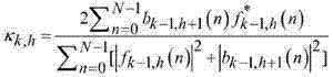
Wherein the superscript denotes conjugation.
The lattice predictor model used for the above-described orthogonal basis function generator 700 can be used to implement the predistorter 110 shown in fig. 1 and 2. In this case, the normalization factors for each node 710, 730 need to be evaluated And reflection coefficient for
 connection node 730 . If the input signalx(n) Is generalized smooth and stable, then can be based onNA continuous input samplex(n) Sequence of (2) estimating the reflection coefficient
 、
、 And a normalization factor. Subsequently, the calculated normalization factors can be statically configured for predistorter 110
 And coefficient of reflection
 . If the input signal is not broadly stationary, the normalization factor may need to be re-evaluated periodically
 And coefficient of reflection
 . In this case, statistics of the input signal may be monitored, and the connection coefficient may be updated periodically. The statistics of the input signal may remain static for a period of time and then change. Thus, once the connection coefficients have been calculated, the connection coefficients can be used to pre-distort the input signal until statistics of the input signal indicate that new connection coefficients are required. As previously described, the reflection coefficients in the lattice model of predistorter 110
 Is considered to be the connection coefficient.
Since the basis function set, the lattice update function and the normalization function are all linear, the predistorter 110 can be equivalently implemented by the orthogonal basis function generator 500 shown in fig. 6. In this case, the reflection coefficients calculated based on the lattice predistorter model of the basis function set、 And a normalization factor
 Can be used to derive connection coefficients for connecting
 nodes 530 in network architecture 500.
Fig. 11 illustrates an exemplary method 800 of pre-distorting an input signal to an electronic device to compensate for distortion caused by the electronic device. The finite sequence of input signal samples is applied to a coefficient evaluation circuit which determines the connected coefficients for the set of orthogonal basis functions modeled as shown in fig. 6 or 8. Based on the input signal samples, the coefficient evaluation circuit computes a set of model coefficients for a two-dimensional lattice prediction model of a set of basis functions (block 810). The lattice prediction model represents the basis functions in the set of predistorter basis functions as different combinations of power basis functions as shown in fig. 10. In one embodiment, the model coefficients include reflection coefficients for a lattice predictor model of orthogonal basis functions as shown in FIG. 10. The model coefficients may be calculated according to equation 17. Subsequently, the coefficient evaluation circuit determines a corresponding set of predistorter connection coefficients from the set of model coefficients to combine the power basis function output signals from the power basis functions to generate the orthogonal basis function output signals (block 820). In one exemplary embodiment, predistorter 110 is based on the same lattice prediction model for the set of basis functions as the coefficient evaluation circuit. In this case, the model coefficients (e.g., reflection coefficients) can be used as predistorter connection coefficients because the two models are the same. In this case, it would also be necessary to periodically evaluate the normalization factor for each connecting node 530. In other embodiments of the present invention, predistorter 110 may implement an equivalent model for a set of basis functions as shown in fig. 6, where the orthogonal basis functions are modeled as sums of power basis function output signals weighted by respective connected coefficients. In this case, the predistorter connection coefficients may be calculated from the model coefficients and corresponding normalization factors derived for the lattice prediction model. The connection coefficients calculated at 820 are then configured for predistorter 110.
As previously described, predistorter 110 is used to predistort input signal samples to compensate for distortion caused by power amplifiers or other nonlinear devices. The input signal is applied to a pre-configured predistorter 110. Predistorter 110 computes a set of power basis function output signals by applying the set of power basis functions to the input signal samples (block 830). The set of predistorter connection coefficients calculated in block 820 is then applied to the power basis function output signals to generate a set of orthogonal basis function output signals (block 840). The basis function output signals are in turn weighted by respective weighting coefficients and combined to generate a predistorted input signal for input to the power amplifier (block 850). It should be noted that the input signal samples predistorted in blocks 830 to 850 need not be the same samples used to derive the connection coefficients in blocks 810 and 820. In practice, statistics of the input signal may be monitored and the connection coefficients may be updated periodically. The statistics of the input signal may remain static for a period of time and then change. Thus, once the connection system has calculated, the connection coefficients can be used to pre-distort the input signal until statistics of the input signal indicate that new connection coefficients are required.
Fig. 12 illustrates an exemplary predistortion circuit 900 according to an exemplary embodiment. The predistortion circuit 900 comprises a predistorter 910, a power amplifier 940, a distortion modeling circuit 950, and a basis function modeling circuit 960 that implement a basis function structure as shown in fig. 4 or 8. Input signalx(n) Is applied to predistorter 910. Predistorter 910 includes a basis function generator 920 and a combiner 930. The basis function generator generates a set of orthogonal basis function output signals from the input signal samples using one of the models shown in fig. 4 and 8. The combiner 930 adds the basis function output signals weighted by the respective weighting coefficients to produce a predistorted input signalz(n). The power amplifier 940 pre-distorts the input signalz(n) Amplifying to generate an output signaly(n). The power amplifier may be operated in a non-linear mode to efficiently amplify the predistorted input signal. The predistortion applied by the predistorter compensates for the distortion caused by the power amplifier such that the cascade of the predistorter and the power amplifier is nearly linear.
The distortion modeling circuit 950 determines the application of the combiner 930 to the basis function output signal to produce a predistorted signalz(n) The weighting coefficient of (2). The distortion modeling circuit 950 may calculate the weighting coefficients by modeling the distortion of the power amplifier or predistorter using well-known techniques described above. In general, distortion modeling circuits use signals that are predistortedz(n) And the output signaly(n) The best-fit distortion model for the power amplifier (direct solution) or predistorter (indirect solution) computes a set of weighting coefficients. Filed concurrently with the present application, entitled "Joint Process Estimator with variable tap delay line for use in Power Amplifier digital predistortion" (Joint Process Estimator with Vari)The co-pending applications of able Tap Delay Line for use in Power Amplifier Digital predictionj, Configurable Basis Function Generation for Nonlinear Modeling (Configurable Basis-Function Generation for Nonlinear Modeling), and Nonlinear Model with Tap Output Normalization (Non-Linear Model with Tap Output Normalization) describe additional techniques for calculating weighting coefficients. These co-pending applications are incorporated herein by reference in their entirety.
Predistorter 910 generates the orthogonal basis function output signals using one of the models shown in fig. 4 and 8, as described above. In either case, the basis function modeling circuit 960 derives the input signal from the input signalx(n) Calculates the connection coefficients to be applied by the basis function model. Thus, the set of basis functions applied to the input signal by predistorter 910 depends on the distribution of the input signal. By matching the orthogonal basis function set to the distribution of the input signal, the matrix generated from the orthogonal basis function set is substantially reduced Condition number of (2). The set of orthogonal basis functions can be implemented using the structure shown in fig. 8 or fig. 8. The structure shown in fig. 6 is backward compatible with a set of power basis functions.
A basis function modeling circuit evaluates a set of orthogonal basis functions based on an actual input signal. Thus, the set of orthogonal basis functions it derives is customized to fit the distribution of the input signal. The condition number of the data matrix is greatly reduced by the proposed set of orthogonal basis functions. For example, analog displays, condition numbers from about 108To about 1.0018. The basis function modeling circuit can be implemented using the orthogonal basis function model shown in fig. 6, which is a general structure and is backward compatible with a set of power basis functions.
The present invention may, of course, be carried out in other specific ways than those herein set forth without departing from the scope and essential characteristics of the invention. The present embodiments are, therefore, to be considered in all respects as illustrative and not restrictive, and all changes coming within the meaning and equivalency range of the appended claims are intended to be embraced therein.
Claims (14)
Applications Claiming Priority (1)
| Application Number | Priority Date | Filing Date | Title |
|---|---|---|---|
| PCT/IB2010/055195 WO2012066383A1 (en) | 2010-11-16 | 2010-11-16 | Orthogonal basis function set for ditigal predistorter |
Publications (2)
| Publication Number | Publication Date |
|---|---|
| CN103299542A true CN103299542A (en) | 2013-09-11 |
| CN103299542B CN103299542B (en) | 2016-03-23 |
Family
ID=44182790
Family Applications (1)
| Application Number | Title | Priority Date | Filing Date |
|---|---|---|---|
| CN201080071096.0A Expired - Fee Related CN103299542B (en) | 2010-11-16 | 2010-11-16 | For the orthogonal basis function collection of digital predistorter |
Country Status (5)
| Country | Link |
|---|---|
| US (2) | US8368466B2 (en) |
| EP (1) | EP2641325B1 (en) |
| CN (1) | CN103299542B (en) |
| CA (1) | CA2817805A1 (en) |
| WO (1) | WO2012066383A1 (en) |
Cited By (3)
| Publication number | Priority date | Publication date | Assignee | Title |
|---|---|---|---|---|
| CN107786174A (en) * | 2016-08-26 | 2018-03-09 | 上海澜至半导体有限公司 | Circuit and method for predistortion |
| CN111082757A (en) * | 2019-12-27 | 2020-04-28 | 东方红卫星移动通信有限公司 | Method for applying adaptive band-limited digital predistortion in broadband satellite communication system |
| CN114374366A (en) * | 2020-10-15 | 2022-04-19 | 大唐移动通信设备有限公司 | Digital pre-distortion processing method and device |
Families Citing this family (29)
| Publication number | Priority date | Publication date | Assignee | Title |
|---|---|---|---|---|
| CA2817805A1 (en) * | 2010-11-16 | 2012-05-24 | Telefonaktiebolaget L M Ericsson (Publ) | Orthogonal basis function set for digital predistorter |
| US8787494B2 (en) | 2012-06-11 | 2014-07-22 | Telefonaktiebolaget L M Ericsson (Publ) | Modeling digital predistorter |
| CN103179074A (en) * | 2013-03-20 | 2013-06-26 | 中国科学院上海微系统与信息技术研究所 | Orthogonal polynomial based adaptive predistortion system and method |
| WO2015107392A1 (en) | 2014-01-16 | 2015-07-23 | Telefonaktiebolaget L M Ericsson (Publ) | Systems and methods for basis function orthogonalization for digital predistortion |
| US9246523B1 (en) * | 2014-08-27 | 2016-01-26 | MagnaCom Ltd. | Transmitter signal shaping |
| WO2016151518A1 (en) * | 2015-03-26 | 2016-09-29 | Telefonaktiebolaget Lm Ericsson (Publ) | Method and apparatus for multiband predistortion using time-shared adaptation loop |
| US11824694B2 (en) | 2015-09-02 | 2023-11-21 | Astrapi Corporation | Systems, devices, and methods employing instantaneous spectral analysis in the transmission of signals |
| US10069664B2 (en) | 2015-09-02 | 2018-09-04 | Astrapi Corporation | Spiral polynomial division multiplexing |
| CA3034804C (en) * | 2015-09-02 | 2023-10-17 | Astrapi Corporation | Spiral polynomial division multiplexing |
| US9590668B1 (en) * | 2015-11-30 | 2017-03-07 | NanoSemi Technologies | Digital compensator |
| CA3059190C (en) | 2016-05-23 | 2023-03-21 | Astrapi Corporation | Method for waveform bandwidth compression |
| US10812166B2 (en) | 2016-10-07 | 2020-10-20 | Nanosemi, Inc. | Beam steering digital predistortion |
| KR20190121825A (en) | 2017-02-25 | 2019-10-28 | 나노세미, 인크. | Multiband Digital Predistorter |
| US10141961B1 (en) | 2017-05-18 | 2018-11-27 | Nanosemi, Inc. | Passive intermodulation cancellation |
| US11115067B2 (en) | 2017-06-09 | 2021-09-07 | Nanosemi, Inc. | Multi-band linearization system |
| US10581470B2 (en) | 2017-06-09 | 2020-03-03 | Nanosemi, Inc. | Linearization system |
| US10931318B2 (en) * | 2017-06-09 | 2021-02-23 | Nanosemi, Inc. | Subsampled linearization system |
| US11323188B2 (en) | 2017-07-12 | 2022-05-03 | Nanosemi, Inc. | Monitoring systems and methods for radios implemented with digital predistortion |
| US11303251B2 (en) | 2017-10-02 | 2022-04-12 | Nanosemi, Inc. | Digital predistortion adjustment based on determination of load condition characteristics |
| JP2021523629A (en) | 2018-05-11 | 2021-09-02 | ナノセミ, インク.Nanosemi, Inc. | Digital compensator for nonlinear systems |
| US10644657B1 (en) | 2018-05-11 | 2020-05-05 | Nanosemi, Inc. | Multi-band digital compensator for a non-linear system |
| CN112640299B (en) | 2018-05-25 | 2024-11-12 | 纳诺塞米有限公司 | Method for digital predistortion, linearization system for performing digital predistortion, and non-transitory machine-readable medium |
| US11863210B2 (en) | 2018-05-25 | 2024-01-02 | Nanosemi, Inc. | Linearization with level tracking |
| US10931238B2 (en) | 2018-05-25 | 2021-02-23 | Nanosemi, Inc. | Linearization with envelope tracking or average power tracking |
| US10848364B2 (en) | 2019-03-06 | 2020-11-24 | Astrapi Corporation | Devices, systems, and methods employing polynomial symbol waveforms |
| US11184201B2 (en) | 2019-05-15 | 2021-11-23 | Astrapi Corporation | Communication devices, systems, software and methods employing symbol waveform hopping |
| US10931403B2 (en) | 2019-05-15 | 2021-02-23 | Astrapi Corporation | Communication devices, systems, software and methods employing symbol waveform hopping |
| EP3826256B1 (en) * | 2019-11-19 | 2023-07-12 | RivieraWaves | Digital pre-distortion method for ofdm-based communication systems |
| US10992326B1 (en) | 2020-05-19 | 2021-04-27 | Nanosemi, Inc. | Buffer management for adaptive digital predistortion |
Citations (4)
| Publication number | Priority date | Publication date | Assignee | Title |
|---|---|---|---|---|
| US6236837B1 (en) * | 1998-07-30 | 2001-05-22 | Motorola, Inc. | Polynomial Predistortion linearizing device, method, phone and base station |
| US6240278B1 (en) * | 1998-07-30 | 2001-05-29 | Motorola, Inc. | Scalar cost function based predistortion linearizing device, method, phone and basestation |
| US20050163250A1 (en) * | 2004-01-27 | 2005-07-28 | Crestcom, Inc. | Distortion-managed digital RF communications transmitter and method therefor |
| US20080144709A1 (en) * | 2006-12-19 | 2008-06-19 | Crestcom, Inc. | RF transmitter with predistortion and method therefor |
Family Cites Families (14)
| Publication number | Priority date | Publication date | Assignee | Title |
|---|---|---|---|---|
| US6798843B1 (en) | 1999-07-13 | 2004-09-28 | Pmc-Sierra, Inc. | Wideband digital predistortion linearizer for nonlinear amplifiers |
| US6504425B1 (en) | 2001-06-07 | 2003-01-07 | Lucent Technologies Inc. | Method and apparatus for modeling and estimating the characteristics of a power amplifier by retaining even-order terms in estimating characteristics |
| US7058369B1 (en) | 2001-11-21 | 2006-06-06 | Pmc-Sierra Inc. | Constant gain digital predistortion controller for linearization of non-linear amplifiers |
| KR100480278B1 (en) | 2002-12-24 | 2005-04-07 | 삼성전자주식회사 | Digital predistorter of a wideband power amplifier and adaptation method therefor |
| US7149257B2 (en) | 2003-07-03 | 2006-12-12 | Powerwave Technologies, Inc. | Digital predistortion system and method for correcting memory effects within an RF power amplifier |
| US7430248B2 (en) | 2004-01-27 | 2008-09-30 | Crestcom, Inc. | Predistortion circuit and method for compensating nonlinear distortion in a digital RF communications transmitter |
| US7577211B2 (en) * | 2004-03-01 | 2009-08-18 | Powerwave Technologies, Inc. | Digital predistortion system and method for linearizing an RF power amplifier with nonlinear gain characteristics and memory effects |
| US7844014B2 (en) | 2006-07-07 | 2010-11-30 | Scintera Networks, Inc. | Pre-distortion apparatus |
| US7899416B2 (en) | 2007-11-14 | 2011-03-01 | Crestcom, Inc. | RF transmitter with heat compensation and method therefor |
| US7688138B2 (en) | 2008-03-24 | 2010-03-30 | Harris Corporation | Electronic device having a predistortion filter and related methods |
| US8369447B2 (en) | 2008-06-04 | 2013-02-05 | Apple Inc. | Predistortion with sectioned basis functions |
| EP2146474A1 (en) | 2008-07-15 | 2010-01-20 | Alcatel, Lucent | A method for calculating predistortion parameters, a transmitter, a base station, a mobile station, and a communication network therefor |
| CA2817805A1 (en) | 2010-11-16 | 2012-05-24 | Telefonaktiebolaget L M Ericsson (Publ) | Orthogonal basis function set for digital predistorter |
| CA2815541A1 (en) | 2010-11-16 | 2012-05-24 | Telefonaktiebolaget Lm Ericsson (Publ) | Joint process estimator with variable tap delay line for use in power amplifier digital predistortion |
-
2010
- 2010-11-16 CA CA2817805A patent/CA2817805A1/en not_active Abandoned
- 2010-11-16 CN CN201080071096.0A patent/CN103299542B/en not_active Expired - Fee Related
- 2010-11-16 WO PCT/IB2010/055195 patent/WO2012066383A1/en not_active Ceased
- 2010-11-16 US US13/119,157 patent/US8368466B2/en not_active Expired - Fee Related
- 2010-11-16 EP EP10805311.7A patent/EP2641325B1/en not_active Not-in-force
-
2013
- 2013-01-25 US US13/749,914 patent/US8610500B2/en active Active
Patent Citations (4)
| Publication number | Priority date | Publication date | Assignee | Title |
|---|---|---|---|---|
| US6236837B1 (en) * | 1998-07-30 | 2001-05-22 | Motorola, Inc. | Polynomial Predistortion linearizing device, method, phone and base station |
| US6240278B1 (en) * | 1998-07-30 | 2001-05-29 | Motorola, Inc. | Scalar cost function based predistortion linearizing device, method, phone and basestation |
| US20050163250A1 (en) * | 2004-01-27 | 2005-07-28 | Crestcom, Inc. | Distortion-managed digital RF communications transmitter and method therefor |
| US20080144709A1 (en) * | 2006-12-19 | 2008-06-19 | Crestcom, Inc. | RF transmitter with predistortion and method therefor |
Cited By (4)
| Publication number | Priority date | Publication date | Assignee | Title |
|---|---|---|---|---|
| CN107786174A (en) * | 2016-08-26 | 2018-03-09 | 上海澜至半导体有限公司 | Circuit and method for predistortion |
| CN111082757A (en) * | 2019-12-27 | 2020-04-28 | 东方红卫星移动通信有限公司 | Method for applying adaptive band-limited digital predistortion in broadband satellite communication system |
| CN111082757B (en) * | 2019-12-27 | 2023-05-23 | 东方红卫星移动通信有限公司 | Method for applying adaptive band-limited digital predistortion in broadband satellite communication system |
| CN114374366A (en) * | 2020-10-15 | 2022-04-19 | 大唐移动通信设备有限公司 | Digital pre-distortion processing method and device |
Also Published As
| Publication number | Publication date |
|---|---|
| US20120119831A1 (en) | 2012-05-17 |
| US8368466B2 (en) | 2013-02-05 |
| WO2012066383A1 (en) | 2012-05-24 |
| US20130154734A1 (en) | 2013-06-20 |
| EP2641325B1 (en) | 2014-08-13 |
| US8610500B2 (en) | 2013-12-17 |
| EP2641325A1 (en) | 2013-09-25 |
| WO2012066383A8 (en) | 2013-03-21 |
| CN103299542B (en) | 2016-03-23 |
| CA2817805A1 (en) | 2012-05-24 |
Similar Documents
| Publication | Publication Date | Title |
|---|---|---|
| CN103299542B (en) | For the orthogonal basis function collection of digital predistorter | |
| CN103201949B (en) | There is tap and export normalized nonlinear model | |
| US20230370937A1 (en) | Method and system for baseband predistortion linearization in multi-channel wideband communication systems | |
| CN103201950B (en) | Joint Process Estimator with Variable Tapped Delay Lines for Power Amplifier Digital Predistortion | |
| US7822146B2 (en) | System and method for digitally correcting a non-linear element | |
| US7729446B2 (en) | System and method for digitally correcting a non-linear element using a multiply partitioned architecture for predistortion | |
| CN100477500C (en) | Power amplifier predistorter and base station comprising same | |
| Le Duc et al. | An adaptive cascaded ILA-and DLA-based digital predistorter for linearizing an RF power amplifier | |
| CA2817801A1 (en) | Configurable basis-function generation for nonlinear modeling | |
| KR20070026478A (en) | Model-Based Distortion Reduction of Power Amplifiers | |
| CN100530944C (en) | Power amplifier pre-distortion | |
| CN102611661B (en) | Predistortion device and method based on precise inverse solution memory polynomial model equation | |
| US20130249631A1 (en) | Memory structure having taps and non-unitary delays between taps | |
| US8645884B2 (en) | Multi-layer memory structure for behavioral modeling in a pre-distorter | |
| JP5260335B2 (en) | Predistorter | |
| CN120907581A (en) | Intelligent compensation method for predistortion of navigation signals | |
| JP2015002418A (en) | Distortion compensation device | |
| Zheng et al. | Adaptive simulator of power amplifier nonlinearity based on piecewise polynomial |
Legal Events
| Date | Code | Title | Description |
|---|---|---|---|
| C06 | Publication | ||
| PB01 | Publication | ||
| C10 | Entry into substantive examination | ||
| SE01 | Entry into force of request for substantive examination | ||
| C14 | Grant of patent or utility model | ||
| GR01 | Patent grant | ||
| CF01 | Termination of patent right due to non-payment of annual fee | ||
| CF01 | Termination of patent right due to non-payment of annual fee |
Granted publication date: 20160323 |