CN1062061A - telephone ringer circuit - Google Patents
telephone ringer circuit Download PDFInfo
- Publication number
- CN1062061A CN1062061A CN91111571A CN91111571A CN1062061A CN 1062061 A CN1062061 A CN 1062061A CN 91111571 A CN91111571 A CN 91111571A CN 91111571 A CN91111571 A CN 91111571A CN 1062061 A CN1062061 A CN 1062061A
- Authority
- CN
- China
- Prior art keywords
- ringer
- output
- transformer
- current
- voltage
- Prior art date
- Legal status (The legal status is an assumption and is not a legal conclusion. Google has not performed a legal analysis and makes no representation as to the accuracy of the status listed.)
- Pending
Links
- 238000004804 winding Methods 0.000 claims description 4
- 239000003990 capacitor Substances 0.000 description 7
- 238000000034 method Methods 0.000 description 5
- 230000000694 effects Effects 0.000 description 3
- 238000010586 diagram Methods 0.000 description 2
- 238000005516 engineering process Methods 0.000 description 1
- 230000005669 field effect Effects 0.000 description 1
- 238000001914 filtration Methods 0.000 description 1
- 238000012423 maintenance Methods 0.000 description 1
- 229910044991 metal oxide Inorganic materials 0.000 description 1
- 150000004706 metal oxides Chemical class 0.000 description 1
- 238000012544 monitoring process Methods 0.000 description 1
- 239000004065 semiconductor Substances 0.000 description 1
Images

Classifications
-
- H—ELECTRICITY
- H03—ELECTRONIC CIRCUITRY
- H03M—CODING; DECODING; CODE CONVERSION IN GENERAL
- H03M1/00—Analogue/digital conversion; Digital/analogue conversion
-
- H—ELECTRICITY
- H03—ELECTRONIC CIRCUITRY
- H03K—PULSE TECHNIQUE
- H03K17/00—Electronic switching or gating, i.e. not by contact-making and –breaking
- H03K17/51—Electronic switching or gating, i.e. not by contact-making and –breaking characterised by the components used
- H03K17/56—Electronic switching or gating, i.e. not by contact-making and –breaking characterised by the components used by the use, as active elements, of semiconductor devices
- H03K17/687—Electronic switching or gating, i.e. not by contact-making and –breaking characterised by the components used by the use, as active elements, of semiconductor devices the devices being field-effect transistors
- H03K17/689—Electronic switching or gating, i.e. not by contact-making and –breaking characterised by the components used by the use, as active elements, of semiconductor devices the devices being field-effect transistors with galvanic isolation between the control circuit and the output circuit
- H03K17/691—Electronic switching or gating, i.e. not by contact-making and –breaking characterised by the components used by the use, as active elements, of semiconductor devices the devices being field-effect transistors with galvanic isolation between the control circuit and the output circuit using transformer coupling
-
- H—ELECTRICITY
- H02—GENERATION; CONVERSION OR DISTRIBUTION OF ELECTRIC POWER
- H02M—APPARATUS FOR CONVERSION BETWEEN AC AND AC, BETWEEN AC AND DC, OR BETWEEN DC AND DC, AND FOR USE WITH MAINS OR SIMILAR POWER SUPPLY SYSTEMS; CONVERSION OF DC OR AC INPUT POWER INTO SURGE OUTPUT POWER; CONTROL OR REGULATION THEREOF
- H02M7/00—Conversion of AC power input into DC power output; Conversion of DC power input into AC power output
- H02M7/42—Conversion of DC power input into AC power output without possibility of reversal
- H02M7/44—Conversion of DC power input into AC power output without possibility of reversal by static converters
- H02M7/48—Conversion of DC power input into AC power output without possibility of reversal by static converters using discharge tubes with control electrode or semiconductor devices with control electrode
- H02M7/53—Conversion of DC power input into AC power output without possibility of reversal by static converters using discharge tubes with control electrode or semiconductor devices with control electrode using devices of a triode or transistor type requiring continuous application of a control signal
- H02M7/537—Conversion of DC power input into AC power output without possibility of reversal by static converters using discharge tubes with control electrode or semiconductor devices with control electrode using devices of a triode or transistor type requiring continuous application of a control signal using semiconductor devices only, e.g. single switched pulse inverters
- H02M7/538—Conversion of DC power input into AC power output without possibility of reversal by static converters using discharge tubes with control electrode or semiconductor devices with control electrode using devices of a triode or transistor type requiring continuous application of a control signal using semiconductor devices only, e.g. single switched pulse inverters in a push-pull configuration
- H02M7/53803—Conversion of DC power input into AC power output without possibility of reversal by static converters using discharge tubes with control electrode or semiconductor devices with control electrode using devices of a triode or transistor type requiring continuous application of a control signal using semiconductor devices only, e.g. single switched pulse inverters in a push-pull configuration with automatic control of output voltage or current
-
- H—ELECTRICITY
- H03—ELECTRONIC CIRCUITRY
- H03K—PULSE TECHNIQUE
- H03K17/00—Electronic switching or gating, i.e. not by contact-making and –breaking
- H03K17/51—Electronic switching or gating, i.e. not by contact-making and –breaking characterised by the components used
- H03K17/56—Electronic switching or gating, i.e. not by contact-making and –breaking characterised by the components used by the use, as active elements, of semiconductor devices
- H03K17/687—Electronic switching or gating, i.e. not by contact-making and –breaking characterised by the components used by the use, as active elements, of semiconductor devices the devices being field-effect transistors
- H03K17/6871—Electronic switching or gating, i.e. not by contact-making and –breaking characterised by the components used by the use, as active elements, of semiconductor devices the devices being field-effect transistors the output circuit comprising more than one controlled field-effect transistor
- H03K17/6872—Electronic switching or gating, i.e. not by contact-making and –breaking characterised by the components used by the use, as active elements, of semiconductor devices the devices being field-effect transistors the output circuit comprising more than one controlled field-effect transistor using complementary field-effect transistors
-
- H—ELECTRICITY
- H04—ELECTRIC COMMUNICATION TECHNIQUE
- H04M—TELEPHONIC COMMUNICATION
- H04M19/00—Current supply arrangements for telephone systems
- H04M19/02—Current supply arrangements for telephone systems providing ringing current or supervisory tones, e.g. dialling tone or busy tone
- H04M19/023—Current supply arrangements for telephone systems providing ringing current or supervisory tones, e.g. dialling tone or busy tone by reversing the polarity of the current at the exchange
Landscapes
- Engineering & Computer Science (AREA)
- Power Engineering (AREA)
- Signal Processing (AREA)
- Theoretical Computer Science (AREA)
- Dc-Dc Converters (AREA)
- Devices For Supply Of Signal Current (AREA)
Abstract
一种用于电话系统的振铃机,包括一个变压器, 该振铃机具有根据振铃机输出控制变压器的初级电 流的第一反馈环路以及根据振铃机输出控制变压器 次级电流的第二反馈环路。

A ringer for a telephone system comprising a transformer having a first feedback loop for controlling the primary current of the transformer based on the output of the ringer and a second feedback loop for controlling the secondary current of the transformer based on the output of the ringer feedback loop.
Description
The present invention relates to be used for the ringer of telephone network.The purposes of ringer provides ringing current and represents to have phone to arrive to the telephone subscriber.
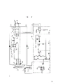
Ringer provides the low-frequency sine electric current, formerly has in the technological system, and ringer adopts primary and secondary HF switch level for example illustrated in figures 1 and 2.
In arrangement shown in Figure 1, elementary a pair of " intermediate voltage track " (the intermediate voltage rail) that provide.Secondary voltage is done pulse width modulation, and its amplitude is between these two voltage rail.Formed modulated voltage waveform passes through filtering again, thereby produces desired output waveform.Here need two HF switch levels, they have reduced efficient and produced high loss when maximum loads; Also need heavy filter element simultaneously.
In Fig. 2, elementaryly be the secondary current source that provides, secondary needs are taked the high frequency modulated technology so that form required output voltage.Output current and secondary current are used to compare, and are used to limit secondary current, thereby have reduced excessive power consumption.There is overcurrent to flow through the shortcoming of output stage when equally also existence needs two HF switch levels and full load here.
The invention provides a kind of ringer that is used for telephone system, it comprises a transformer with first and second feedback control loops, first feedback control loop is used for the primary current according to ringer output control transformer, and second feedback control loop is used for the secondary current according to ringer output control transformer.
Now narrate one embodiment of the present of invention by example (and with reference to accompanying drawing), these accompanying drawings are:
Fig. 1 and Fig. 2, this is the circuit theory diagrams of the ringer of the top expression prior art of having narrated;
Fig. 3 is the ringer circuit schematic diagram that expression is used for the topological structure of present embodiment;
Fig. 4 is the Lu Lingji that shakes that has comprised the control loop of the topological structure that adopts Fig. 3.
In Fig. 3, show a feedback current transformer that is used to provide current source I+ and I-, these current sources are comprised the control of the secondary switch level of pair of metal oxide semiconductor field effect transistor (MOSFET) 7 and 8.Output waveform is subjected to the control of two voltage feedback loop 13 and 18, makes circuit that two kinds of working methods be arranged.When the ringing current Iac of the enough amplitudes of needs, inner control loop 18 will be modulated so that keep the amplitude of output waveform primary current.Output control loop 13 one of will only keep in a pair of MOSFET 7 and 8 conducting in the whole half period of output waveform, thereby suitable power supply polarity is provided.
Secondary current flows through by MOSFET 7 or 8 selected paths.Output capacitor 6 is charged rightly, thereby produce needed output waveform.When the big electric current of needs the electric current of circulation not taking place, thereby reaches high efficiency, low-power consumption and low noise.
When not needing or only needing very little ringer electric current, secondary MOSFET 7 and 8 operating state are from becoming as high-frequency modulator as polarity switch.Why these needs are arranged, be because the voltage on the output electrical equipment 6 does not have discharge path in the back half the time of every half period when not having load current, thereby can not keep the cause of sinusoidal output waveform.In the process under these light load condition, the electric current of circulation does not expend very much.
Though the present invention is described with reference to a feedback current transformer, can adopt the topological structure of various replacements.
Referring to Fig. 4, wherein outer control loop 13 comprises a voltage divider 9, and this voltage divider 9 is used for the output-voltage levels on the monitoring capacitor 6.The intermediate point of the output of baseline sinusoidal wave oscillator 10 and voltage divider 9 is all received a differential amplifier 11 that plays the comparator effect.Differential amplifier 11 produces the output error voltage of the difference of two input of indication.This is output in is by trigger 12 and a clock synchronization.So just any state is provided the minimum duration that equals 5 microseconds, and doubly value of taking advantage of that any longer duration all is this basic time.
Resulting should the outer output of controlling loop 13 being fed on the grid of a pair of MOSFET 7 and 8 as switching voltage.The circuit structure of these MOSFET makes that another just only carries when one of them conducting.These MOSFET provide a path, make that output capacitor 6 can be by suitable polarity charging.MOSFET7 allows through diode 4 positive charge, and MOSFET 8 allows through the charging of diode 5 negative senses.Needed charging current is provided by feedback transformer 3, and this Secondary winding of transformer is coupled and form suitable path.It should be noted that transformer secondary output inductance and output capacitor 6 constitute a low pass filter, thereby can obtain slick and sly output voltage waveforms.
When not needing or only needing very little ringer electric current I ac, the voltage on the output capacitor 6 is not kept the external discharge path of sinusoidal output waveform.Control loop 13 will change its duty cycle (duty cycle) so that the correct magnitude of voltage on the maintenance capacitor 6.Balance is kept in two inputs of comparator 11 easily, thereby Light Condition occurs.Like this, there are repeatedly charge and discharge in capacitor in the half period of output waveform, thereby exists loop current.
Each input of delivering to differential amplifier 11 also is fed to inner control loop 18.Inner control loop 18 comprises a differential amplifier 14, and this differential amplifier 14 amplifies the difference signal of baseline sinusoidal wave amplifier 10 and the output of voltage divider 9 intermediate points.The output of differential amplifier 14 is fed to full-wave rectifier 15 again and goes, from the error voltage of an one pole of these full-wave rectifier 15 outputs.Then be a voltage-controlled current source 16, it plays level skew effect, thereby an error voltage Ve is provided to pulse width modulator 17.
Pulse width modulator 17 makes elementary MOSFET 1 conducting, so the primary current of feedback transformer 3 is increased.This electric current is detected by resistor 2 and is used to make pulse width modulator 17 to reset, thereby provides the current work mode to control.The big or small given corresponding pulse duration of confessing by pulse width modulator 17 of error voltage Ve, thereby limit elementary peak current.So this primary current transforms to secondary winding by the feedback effect of transformer 3.
When requiring ringer electric current I ac to increase, need bigger primary current.This current increases by increase be fed to pulse width modulator 17 error voltage Ve, and thereby by the increase inner control loop 18 input signal between whole difference realize, because these input signals of inner control loop 18 also are fed to the comparator 11 of outer control loop 13 and go, make the especially big offset of appearance between two inputs of comparator 11.This situation will make comparator 11 remain on a kind of state, thereby will keep conducting in the complete half period of output waveform one of in a pair of MOSFET 7 and 8.When output changed through zero point, the offset on the comparator 11 changed polarity and impels MOSFET conducting in the next half period of inverse state.
Under this working method, output switching stage MOSFET 7 and 8 only is a polarity switch, and output amplitude is to be produced by the elementary inner control loop 18 of modulation fully.So just obtained high efficiency and thereby the loss when requiring the dynamo-electric stream of big ring very low.
By adopting feedback converter topologies by two voltage feedback loop controls, a kind of circuit with two kinds of working methods is provided, these two kinds of working methods depend on the size of the load current of needs.When the big electric current of needs, only need with a HF switch level so that produce output voltage waveforms, make circuit have high efficiency and its circuit arrangement small-sized correspondingly.
Claims (5)
Applications Claiming Priority (2)
| Application Number | Priority Date | Filing Date | Title |
|---|---|---|---|
| GB9026504.2 | 1990-12-05 | ||
| GB909026504A GB9026504D0 (en) | 1990-12-05 | 1990-12-05 | Telephone ringer circuit |
Publications (1)
| Publication Number | Publication Date |
|---|---|
| CN1062061A true CN1062061A (en) | 1992-06-17 |
Family
ID=10686559
Family Applications (1)
| Application Number | Title | Priority Date | Filing Date |
|---|---|---|---|
| CN91111571A Pending CN1062061A (en) | 1990-12-05 | 1991-12-05 | telephone ringer circuit |
Country Status (10)
| Country | Link |
|---|---|
| EP (1) | EP0489512A3 (en) |
| JP (1) | JPH04340841A (en) |
| KR (1) | KR920013934A (en) |
| CN (1) | CN1062061A (en) |
| AU (1) | AU651398B2 (en) |
| CA (1) | CA2056132A1 (en) |
| FI (1) | FI915711A7 (en) |
| GB (2) | GB9026504D0 (en) |
| IE (1) | IE914004A1 (en) |
| PT (1) | PT99681A (en) |
Families Citing this family (3)
| Publication number | Priority date | Publication date | Assignee | Title |
|---|---|---|---|---|
| DE4218845C2 (en) * | 1992-06-09 | 1994-10-27 | Bosch Telecom | Circuit arrangement for a ringing voltage generator |
| DE19740137A1 (en) * | 1997-09-12 | 1999-03-18 | Alsthom Cge Alcatel | Method and circuit arrangement for generating alternating calls for electronic subscriber circuits |
| US6252787B1 (en) | 2000-05-12 | 2001-06-26 | Honeywell International Inc. | Controllable circuit for providing bi-directional current to a load |
Family Cites Families (2)
| Publication number | Priority date | Publication date | Assignee | Title |
|---|---|---|---|---|
| GB8606151D0 (en) * | 1986-03-12 | 1986-04-16 | Gen Electric Co Plc | Telephone system circuit |
| US4890210A (en) * | 1988-11-15 | 1989-12-26 | Gilbarco, Inc. | Power supply having combined forward converter and flyback action for high efficiency conversion from low to high voltage |
-
1990
- 1990-12-05 GB GB909026504A patent/GB9026504D0/en active Pending
-
1991
- 1991-11-15 EP EP19910310581 patent/EP0489512A3/en not_active Withdrawn
- 1991-11-15 GB GB9124299A patent/GB2250663B/en not_active Expired - Lifetime
- 1991-11-18 IE IE400491A patent/IE914004A1/en not_active Application Discontinuation
- 1991-11-26 CA CA002056132A patent/CA2056132A1/en not_active Abandoned
- 1991-12-02 JP JP3343888A patent/JPH04340841A/en active Pending
- 1991-12-04 FI FI915711A patent/FI915711A7/en not_active Application Discontinuation
- 1991-12-04 AU AU88854/91A patent/AU651398B2/en not_active Ceased
- 1991-12-04 PT PT99681A patent/PT99681A/en not_active Application Discontinuation
- 1991-12-04 KR KR1019910022137A patent/KR920013934A/en not_active Withdrawn
- 1991-12-05 CN CN91111571A patent/CN1062061A/en active Pending
Also Published As
| Publication number | Publication date |
|---|---|
| FI915711L (en) | 1992-06-06 |
| AU651398B2 (en) | 1994-07-21 |
| FI915711A7 (en) | 1992-06-06 |
| PT99681A (en) | 1994-01-31 |
| EP0489512A3 (en) | 1993-03-24 |
| EP0489512A2 (en) | 1992-06-10 |
| AU8885491A (en) | 1992-06-11 |
| GB2250663A (en) | 1992-06-10 |
| FI915711A0 (en) | 1991-12-04 |
| GB9124299D0 (en) | 1992-01-08 |
| GB9026504D0 (en) | 1991-01-23 |
| KR920013934A (en) | 1992-07-30 |
| GB2250663B (en) | 1995-04-19 |
| IE914004A1 (en) | 1992-06-17 |
| JPH04340841A (en) | 1992-11-27 |
| CA2056132A1 (en) | 1992-06-06 |
Similar Documents
| Publication | Publication Date | Title |
|---|---|---|
| CN100541995C (en) | Power Factor Improvement Circuit | |
| US6034513A (en) | System and method for controlling power factor and power converter employing the same | |
| EP0553179B1 (en) | Dc/ac converter | |
| US7279868B2 (en) | Power factor correction circuits | |
| Lai et al. | A general constant-frequency pulsewidth modulator and its applications | |
| WO1996007960A1 (en) | A synchronous switching cascade connected offline pfc-pwm combination power converter controller | |
| US20230299660A1 (en) | Switching sequence controlled current steering for stacked half bridge converters | |
| CN107612326A (en) | A kind of Sofe Switch modulator approach of two-way tandem type Buck Boosts | |
| CN115534715B (en) | A constant current and constant voltage IPT system with configurable charging voltage and charging current | |
| Redl et al. | Small-signal dynamic analysis of regulated class-E dc/dc converters | |
| CN107026568A (en) | control circuit, control method and switching power supply | |
| CN118316326A (en) | Current decoupling control method for auxiliary inductance double-step-down half-bridge power amplifier | |
| CN201750341U (en) | Radio frequency power supply with adjustable output voltage | |
| US8760230B2 (en) | Switching amplifier with pulsed current source and sink | |
| US9602067B2 (en) | Switching amplifier with pulsed current supply | |
| CN1062061A (en) | telephone ringer circuit | |
| CN106655840B (en) | three-phase current type PWM rectifier control method for reducing average switching rate | |
| CN104640268A (en) | High-power-factor constant-current control circuit and LED (light emitting diode) illuminating equipment | |
| CN119010560A (en) | Four-pipe Buck-Boost PFC converter control method and control circuit | |
| CN118117880A (en) | A New Quasi-Single-Stage Converter | |
| EP4718704A1 (en) | Rectifier with inherent unity power factor | |
| KR100292489B1 (en) | Power factor correcting boost converter using soft switching technique | |
| Li et al. | A pulse density modulation method for ZVS full-bridge converters in wireless power transfer systems | |
| CN114337327B (en) | Power decoupling circuit, power supply and electronic equipment | |
| Ting et al. | A soft switching power factor correction interleaved AC-DC boost converter |
Legal Events
| Date | Code | Title | Description |
|---|---|---|---|
| C06 | Publication | ||
| PB01 | Publication | ||
| C01 | Deemed withdrawal of patent application (patent law 1993) | ||
| WD01 | Invention patent application deemed withdrawn after publication |