CN113607043A - Strain gauge for chip stress test - Google Patents

Strain gauge for chip stress test Download PDF

Info

Publication number
CN113607043A
CN113607043A CN202110872718.XA CN202110872718A CN113607043A CN 113607043 A CN113607043 A CN 113607043A CN 202110872718 A CN202110872718 A CN 202110872718A CN 113607043 A CN113607043 A CN 113607043A
Authority
CN
China
Prior art keywords
strain gauge
strain
strain gage
chip
grids
Prior art date
Legal status (The legal status is an assumption and is not a legal conclusion. Google has not performed a legal analysis and makes no representation as to the accuracy of the status listed.)
Pending
Application number
CN202110872718.XA
Other languages
Chinese (zh)
Inventor
晏志鹏
雷宇哲
刘忙贤
雒平华
赵凯锋
Current Assignee (The listed assignees may be inaccurate. Google has not performed a legal analysis and makes no representation or warranty as to the accuracy of the list.)
Zhonghang Electronic Measuring Instruments Co Ltd
Original Assignee
Zhonghang Electronic Measuring Instruments Co Ltd
Priority date (The priority date is an assumption and is not a legal conclusion. Google has not performed a legal analysis and makes no representation as to the accuracy of the date listed.)
Filing date
Publication date
Application filed by Zhonghang Electronic Measuring Instruments Co Ltd filed Critical Zhonghang Electronic Measuring Instruments Co Ltd
Priority to CN202110872718.XA priority Critical patent/CN113607043A/en
Publication of CN113607043A publication Critical patent/CN113607043A/en
Pending legal-status Critical Current

Links

Images

Classifications

    • GPHYSICS
    • G01MEASURING; TESTING
    • G01BMEASURING LENGTH, THICKNESS OR SIMILAR LINEAR DIMENSIONS; MEASURING ANGLES; MEASURING AREAS; MEASURING IRREGULARITIES OF SURFACES OR CONTOURS
    • G01B7/00Measuring arrangements characterised by the use of electric or magnetic techniques
    • G01B7/16Measuring arrangements characterised by the use of electric or magnetic techniques for measuring the deformation in a solid, e.g. by resistance strain gauge
    • G01B7/18Measuring arrangements characterised by the use of electric or magnetic techniques for measuring the deformation in a solid, e.g. by resistance strain gauge using change in resistance
    • GPHYSICS
    • G01MEASURING; TESTING
    • G01LMEASURING FORCE, STRESS, TORQUE, WORK, MECHANICAL POWER, MECHANICAL EFFICIENCY, OR FLUID PRESSURE
    • G01L1/00Measuring force or stress, in general
    • G01L1/20Measuring force or stress, in general by measuring variations in ohmic resistance of solid materials or of electrically-conductive fluids; by making use of electrokinetic cells, i.e. liquid-containing cells wherein an electrical potential is produced or varied upon the application of stress
    • G01L1/22Measuring force or stress, in general by measuring variations in ohmic resistance of solid materials or of electrically-conductive fluids; by making use of electrokinetic cells, i.e. liquid-containing cells wherein an electrical potential is produced or varied upon the application of stress using resistance strain gauges
    • GPHYSICS
    • G01MEASURING; TESTING
    • G01LMEASURING FORCE, STRESS, TORQUE, WORK, MECHANICAL POWER, MECHANICAL EFFICIENCY, OR FLUID PRESSURE
    • G01L9/00Measuring steady of quasi-steady pressure of fluid or fluent solid material by electric or magnetic pressure-sensitive elements; Transmitting or indicating the displacement of mechanical pressure-sensitive elements, used to measure the steady or quasi-steady pressure of a fluid or fluent solid material, by electric or magnetic means
    • G01L9/02Measuring steady of quasi-steady pressure of fluid or fluent solid material by electric or magnetic pressure-sensitive elements; Transmitting or indicating the displacement of mechanical pressure-sensitive elements, used to measure the steady or quasi-steady pressure of a fluid or fluent solid material, by electric or magnetic means by making use of variations in ohmic resistance, e.g. of potentiometers, electric circuits therefor, e.g. bridges, amplifiers or signal conditioning
    • G01L9/04Measuring steady of quasi-steady pressure of fluid or fluent solid material by electric or magnetic pressure-sensitive elements; Transmitting or indicating the displacement of mechanical pressure-sensitive elements, used to measure the steady or quasi-steady pressure of a fluid or fluent solid material, by electric or magnetic means by making use of variations in ohmic resistance, e.g. of potentiometers, electric circuits therefor, e.g. bridges, amplifiers or signal conditioning of resistance-strain gauges

Landscapes

  • Physics & Mathematics (AREA)
  • General Physics & Mathematics (AREA)
  • Measurement Of Length, Angles, Or The Like Using Electric Or Magnetic Means (AREA)

Abstract

本发明公开了一种用于芯片应力测试用应变计,包括设置在同一应变计基底上的4~20组测量栅,每行设置四组测量栅,每组测量栅包括至少三个不同方向的单轴测量栅。通过在应变计基底上的4~20组测量栅,将测量栅进行排布,每组测量栅包括至少三个不同方向的单轴测量栅,从而在应变计有限的面积中,增加应变计的测试点,可实现对待测物不同梯度、各个方向上受力状况的测量,提高测试结果的准确性。

Figure 202110872718

The invention discloses a strain gauge for chip stress testing, comprising 4 to 20 groups of measurement grids arranged on the same strain gauge substrate, four groups of measurement grids are arranged in each row, and each group of measurement grids includes at least three measurement grids in different directions. Uniaxial measurement grid. The measurement grids are arranged through 4 to 20 groups of measurement grids on the strain gauge substrate, each group of measurement grids includes at least three uniaxial measurement grids in different directions, thereby increasing the strain gage in the limited area of the strain gauge. The test point can realize the measurement of different gradients and force conditions of the object to be tested in all directions, and improve the accuracy of the test results.

Figure 202110872718

Description

Strain gauge for chip stress test
Technical Field
The invention belongs to the field of strain gauges, and relates to a strain gauge for chip stress test.
Background
In order to prevent various possible failure problems of the chip (such as BGA chip mounting, circuit board mounting stress, mechanical vibration and the like), quantitatively evaluating and identifying harmful processes of the chip with excessive stress in the processes of component assembly, testing, mechanical mounting, transportation and the like, the stress distribution condition of the chip under various stress states needs to be tested.
The common resistance strain gauge can realize the measurement of the stress distribution of a part to be tested, and the strain gauges for the test mainly comprise three types: firstly, a plurality of single-axis strain gauges are arranged, secondly, overlapped pattern type strain gauges are used, and thirdly, strain patterns of 3-8 groups of measuring grids are used.
In the process of chip testing, the existing strain gauge is used, and the following problems mainly exist: the surface area of the chip is small, the arrangement area of the strain gauge is limited, more test points cannot be arranged, the test result cannot reflect the stress-strain distribution condition, and the difference between the stress-strain distribution condition and the stress distribution cloud chart is large.
Disclosure of Invention
The invention aims to overcome the defects of the prior art and provide the strain gauge for the chip stress test, so that the test points of the strain gauge are increased, and the accuracy of the test result is improved.
In order to achieve the purpose, the invention adopts the following technical scheme to realize the purpose:
the strain gauge for the chip stress test comprises 4-20 groups of measurement grids arranged on the same strain gauge substrate, wherein an even number of groups of measurement grids are arranged in each row, and each group of measurement grids comprises at least three uniaxial measurement grids in different directions.
Preferably, each single-axis measuring grid is provided with a weld spot, which is provided on two opposite sides or four sides of the strain gauge.
Preferably, the included angle between the uniaxial measurement grids is 0-180 ℃.
Preferably, the resistance of each uniaxial measurement grid is in the range of 120 Ω to 1000 Ω.
Preferably, the distance between each group of measuring grids is 4-10 mm.
Preferably, the strain gauge comprises 2-4 same strain gauge substrates, 4-20 groups of measurement grids are equally divided by all the strain gauge substrates, and the strain gauges are bonded among all the strain gauge substrates.
Preferably, a heat sink is placed on top of the strain gage, with the strain gage pads outside the area of the chip package or capped heat sink.
Preferably, the strain gauge comprises a base film and a cover film, wherein the base film and the cover film are phenolic resin, epoxy resin, polyurethane, polyether-ether-ketone or polyimide films with the thickness of 10-50 μm.
Preferably, the strain gauge is connected to the test instrument in a three wire system.
Preferably, the welding spot of the strain gauge is connected with one end of a connecting wire, the other end of the connecting wire is connected with a test wire, and the diameter and the hardness of the connecting wire are both smaller than those of the test wire.
Compared with the prior art, the invention has the following beneficial effects:
according to the invention, the measurement grids are arranged through 4-20 groups of measurement grids on the substrate of the strain gauge, each group of measurement grids comprises at least three uniaxial measurement grids in different directions, so that the test points of the strain gauge are increased in the limited area of the strain gauge, the measurement of the stress conditions of the object to be tested in different gradients and all directions can be realized, and the accuracy of the test result is improved.
Furthermore, the welding points of the strain gauge can be led out from two sides for arrangement. And when the number of welding spots is more, the welding spots can be arranged in a four-side lead-out mode.
Furthermore, the strain gauge is split, so that the number of the measurement grids on each measurement grid substrate is not too large, and the preparation difficulty is reduced.
Furthermore, the welding spot is designed outside the chip packaging or capping heat radiator area, so that the welding spot can be prevented from influencing the surface attachment of the heat radiator chip.
Furthermore, the base film and the cover film which are thinner can enable the strain gauge to be better attached to the surface of the chip with curvature.
Furthermore, the strain gauge and the testing instrument are connected in a three-wire system mode, so that the influence of the resistance of a connecting wire between the strain gauge and the testing instrument on a testing result can be reduced.
Furthermore, the thin and soft connecting lead is led out from the welding point and then is connected with the test lead in a switching mode, so that the connection reliability of the lead in the drop test is guaranteed.
Drawings
FIG. 1 is a schematic view of the strain gage measurement grating of this patent.
Fig. 2 is a schematic diagram of the strain gauge of this patent divided into four pieces.
Fig. 3 is a schematic diagram of two-side lead-out arrangement of solder joints in the present patent.
FIG. 4 is a schematic diagram of the solder joint four-side lead-out arrangement of this patent.
Fig. 5 is a schematic diagram of a first three wire connection for the strain gage of this patent.
Fig. 6 is a schematic diagram of a second three wire connection for the strain gage of this patent.
FIG. 7 is a diagram illustrating a first application state of a strain gauge according to the present invention.
Fig. 8 is a diagram illustrating a second application state of the strain gauge according to the present invention.
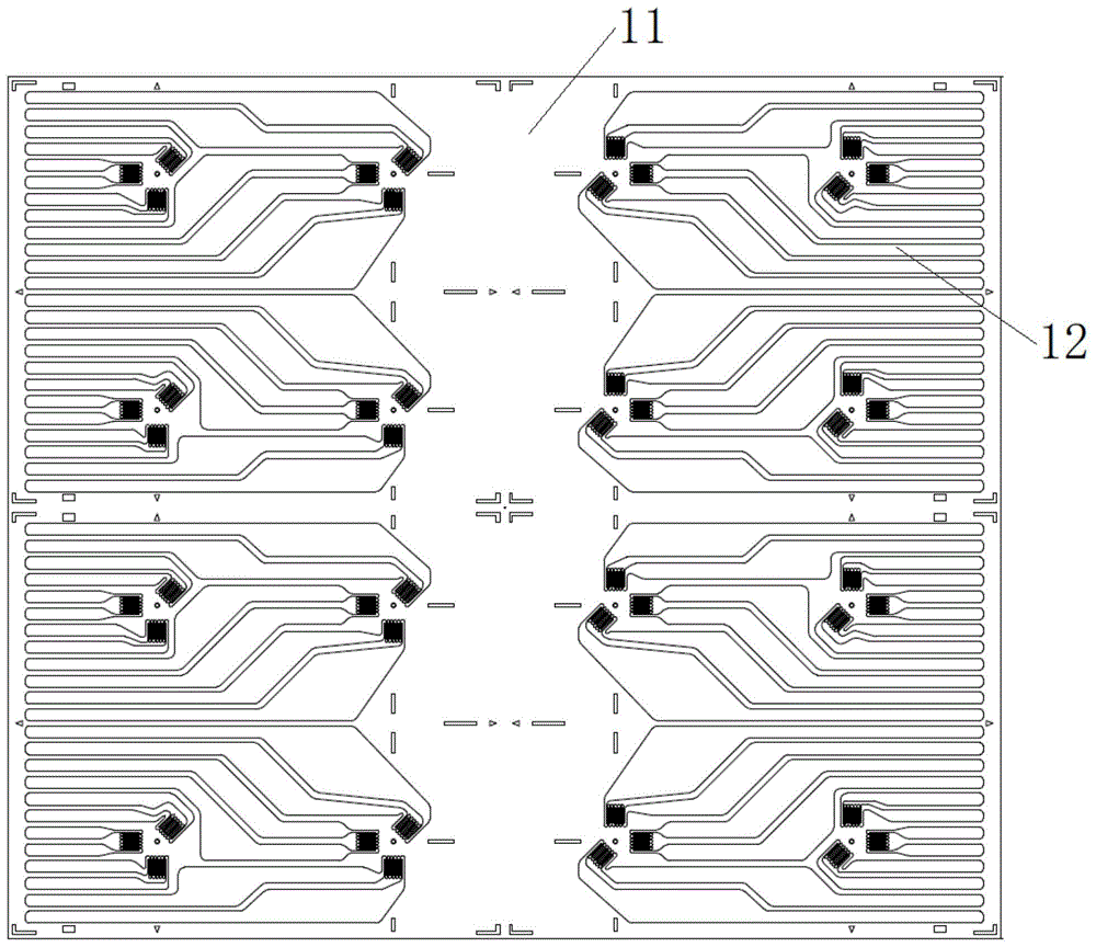
Wherein: 1-radiator, 2-chip body, 3-chip substrate, 4-PCB, 5-strain gauge, 6-patch glue layer, 7-welding spot, 8-strain gauge lead, 9-connecting lead and 10-testing lead; 11-a strain gauge substrate; 12-measuring grid.
Detailed Description
The invention is described in further detail below with reference to the accompanying drawings:
the strain gauge 5 for the chip stress test comprises 4-20 groups of measurement grids 12 arranged on the same strain gauge substrate 11, wherein the distance between each group of measurement grids 12 is as follows: 4-10 mm. Each row is provided with a plurality of groups of measuring grids 12, each group of measuring grids 12 comprises 3 or more single-axis measuring grids in different directions, and the included angle between the single-axis measuring grids is 0-180 ℃. The resistance of each uniaxial measuring grid ranges from 120 omega to 1000 omega, and the welding points 7 led out by each grid can be distributed in the four sides of the whole strain gauge 5.
As shown in fig. 1, the strain gauge 5 of this embodiment is designed with 16 sets of measurement grids 12 at regular intervals in a region of 27 × 26mm, wherein each set includes 3 uniaxial measurement grids in different directions, and the 3 uniaxial measurement grids are 0 ° direction, 90 ° direction and 135 ° direction in total for 48 uniaxial measurement grids.
If the strain gauge 5 is provided with too many measurement grids 12, it may cause difficulty in manufacturing the strain gauge 5. At this time, the whole strain gauge 5 can be divided into 2-4 pieces according to the repeatability of the measuring grid 12, and after each piece is manufactured independently, the pieces are bonded together according to the graph before division through the cover layer, so that the strain gauge 5 with complete graph is formed.
As shown in fig. 2, the pattern in fig. 1 is divided into 4 pieces, each piece is separately produced, and the pieces are bonded together by a cover layer according to the pattern before division to form the strain gauge 5 with a complete pattern. The strain gauge 5 can achieve the testing effect of the strain gauge 5 in fig. 1, and the production and the manufacture are easier.
The single-axis measuring grids are provided with welding spots 7, and the welding spots 7 are arranged on two opposite sides or four sides of the strain gauge 5.
Fig. 3 and 4 show two arrangements of the solder bumps 7 present in the present invention. The welding points 7 of the strain gauge 5 can be led out from two sides for arrangement. And when the number of the welding spots 7 is large, the welding spots can be arranged in a four-side lead-out mode.
The solder joints 7 affect the adhesion of the heat spreader 1 to the surface of the chip. By designing the location of the solder joints 7 outside the area of the chip package or capped heat sink 1, the influence of the solder joints 7 can be avoided.
The thickness of the strain gauge 5 affects its own adherence to the chip surface. When selecting materials, the base film with thinner thickness is selected, so that the strain gauge 5 can be better attached to the surface of the chip with curvature. The base film and the cover film with proper thickness are selected, and the phenolic resin, the epoxy resin, the polyurethane, the polyether ether ketone or the polyimide film with the thickness of 10-50 mu m is adopted.
In order to reduce the influence of the resistance of the connecting lead 9 between the strain gauge 5 and the strain gauge for acquiring data on the test result, a three-wire system mode is adopted for connection. One scheme is as follows: each uniaxial measuring grid is designed with two welding spots 7, one of which leads out a conducting wire and the other leads out two conducting wires. The other scheme is as follows: each uniaxial measuring grid is designed with three welding points 7, and each welding point 7 leads out a conducting wire.
As shown in fig. 4, when only two solder joints 7 are designed for each uniaxial sensitive grid, the three-wire method is: two wires are led out from one welding point 7, and one wire is led out from the other welding point 7.
As shown in fig. 5, three welding points 7 can be designed for each single-axis sensitive grating when the strain gauge 5 is designed graphically, and the three-wire connection method is as follows: each welding point 7 is led out by a lead.
Solder joint 7 is connected with strainometer wire 8, and for guaranteeing that the wire is connected reliably in falling, strainometer wire 8 includes connecting wire 9 and test wire 10, and accessible solder joint 7 draws connecting wire 9 earlier and switching test wire 10 again, and connecting wire 9 diameter and hardness all are less than test wire 10, fixes partial wire on PCB board 4 simultaneously, guarantees the reliability of wire connection in the test process.
When the strain gauge 5 is connected with a lead, the part led out from the welding point 7 is firstly connected with a short (200 mm-500 mm) section of connecting lead 9, so that the stress concentration at the welding point 7 caused by the hard lead is avoided. The connection lead 9 is preferably silver-plated wire, enameled wire, polytetrafluoroethylene wire, or PVC wire with a diameter of 0.3mm or less. After the connecting wire 9 is connected, a longer (1000 mm-5000 mm) section of testing wire 10 is connected, and the testing wire 10 recommends using three-core PVC, TPE and polytetrafluoroethylene flat cables with the diameter phi of 0.3 mm-phi 1.5 mm.
Fig. 7 and 8 show the application of the strain gauge 5 in a chip stress testing device, the chip stress testing device comprises a radiator 1, the strain gauge 5, a patch adhesive layer 6, a chip body 2, a chip substrate 3 and a PCB 4 which are sequentially arranged from top to bottom, the strain gauge 5 is fixed on a concave or convex chip with different curvatures on the surface by using the patch adhesive, the radiator 1 is covered above the strain gauge 5, and the chip is fixed on the PCB 4 through the substrate. The welding spot 7 is positioned outside the contact area of the radiator 1 and the chip, a strain gauge lead 8 is led out of the welding spot 7, and the tail end of the lead is connected with a test instrument.
The strain gauge 5 design technology for chip stress testing is combined with the strain gauge 5 manufacturing technology and the stress testing technology, so that the accurate adjustment and measurement of the stress distribution of the chip can be realized. Through tests, the repeatability (the average value/standard deviation of 3 times of tests) of the strain gauge 5 is within-2% to + 2%, and the stress distribution conditions of the chip under different falling states can be reflected in real time.
Table 1 loading repetitive data record table
Figure BDA0003189331350000061
The above-mentioned contents are only for illustrating the technical idea of the present invention, and the protection scope of the present invention is not limited thereby, and any modification made on the basis of the technical idea of the present invention falls within the protection scope of the claims of the present invention.

Claims (10)

1. The strain gauge for the chip stress test is characterized by comprising 4-20 groups of measuring grids (12) arranged on the same strain gauge substrate (11), wherein each row is provided with a plurality of groups of measuring grids (12), and each group of measuring grids (12) comprises at least three uniaxial measuring grids in different directions.
2. The strain gage for chip stress testing according to claim 1, wherein each uniaxial measuring grid is provided with a solder joint (7), the solder joints (7) being provided on two opposite sides or four sides of the strain gage (5).
3. The strain gauge for chip stress test according to claim 1, wherein the included angle between the uniaxial measurement grids is 0-180 ℃.
4. The strain gage for chip stress testing according to claim 1, wherein each uniaxial measuring grid has a resistance ranging from 120 Ω to 1000 Ω.
5. The strain gauge for chip stress test according to claim 1, wherein the distance between each group of the measuring grids (12) is 4-10 mm.
6. The strain gage for chip stress test according to claim 1, wherein the strain gage (5) comprises 2-4 identical strain gage substrates (11), all the strain gage substrates (11) divide 4-20 groups of measuring grids (12) equally, and all the strain gage substrates (11) are bonded to form the strain gage (5).
7. The strain gage for chip stress testing according to claim 1, wherein the strain gage (5) is provided with a heat sink (1) on top, and the solder joint (7) of the strain gage (5) is outside the area of the chip package or the capped heat sink (1).
8. The strain gauge for chip stress test as claimed in claim 1, wherein the strain gauge (5) comprises a base film and a cover film, and the base film and the cover film are phenolic resin, epoxy resin, polyurethane, polyetheretherketone or polyimide films with a thickness of 10 μm-50 μm.
9. The strain gage for chip stress test according to claim 1, wherein the strain gage (5) is connected with the test instrument in a three-wire system.
10. The strain gauge for chip stress test according to claim 1, wherein the solder joint (7) of the strain gauge (5) is connected with one end of a connecting lead (9), the other end of the connecting lead (9) is connected with a test lead (10), and the diameter and hardness of the connecting lead (9) are smaller than those of the test lead (10).
CN202110872718.XA 2021-07-30 2021-07-30 Strain gauge for chip stress test Pending CN113607043A (en)

Priority Applications (1)

Application Number Priority Date Filing Date Title
CN202110872718.XA CN113607043A (en) 2021-07-30 2021-07-30 Strain gauge for chip stress test

Applications Claiming Priority (1)

Application Number Priority Date Filing Date Title
CN202110872718.XA CN113607043A (en) 2021-07-30 2021-07-30 Strain gauge for chip stress test

Publications (1)

Publication Number Publication Date
CN113607043A true CN113607043A (en) 2021-11-05

Family

ID=78338740

Family Applications (1)

Application Number Title Priority Date Filing Date
CN202110872718.XA Pending CN113607043A (en) 2021-07-30 2021-07-30 Strain gauge for chip stress test

Country Status (1)

Country Link
CN (1) CN113607043A (en)

Citations (9)

* Cited by examiner, † Cited by third party
Publication number Priority date Publication date Assignee Title
CN1648626A (en) * 2004-01-27 2005-08-03 梅特勒-托莱多有限公司 Moisture protection for electromechanical sensors
CN102435361A (en) * 2011-10-27 2012-05-02 扬州晶新微电子有限公司 Method for testing residual stress of silicon single crystal wafer
EP2490036A1 (en) * 2011-02-18 2012-08-22 Melexis Technologies NV Stress sensor for measuring mechanical stresses in a semiconductor chip and stress compensated Hall sensor
US20140085740A1 (en) * 2011-01-26 2014-03-27 Alpao Deformable mirror with capacitive sensors
US20140336969A1 (en) * 2011-12-29 2014-11-13 Alpao Common calibration system and corresponding method
CN106949827A (en) * 2017-03-09 2017-07-14 华中科技大学 A kind of array resistance strain sensor and the measurement compensation system with the sensor
CN110806172A (en) * 2019-12-06 2020-02-18 中国工程物理研究院化工材料研究所 Sensor, preparation method thereof and integrated strain temperature sensing and measuring system
US20200211914A1 (en) * 2018-12-31 2020-07-02 Micron Technology, Inc. Method and apparatus for on-chip stress detection
CN112097632A (en) * 2020-09-18 2020-12-18 江苏东华测试技术股份有限公司 Nonlinear correction method for constant-voltage bridge for large strain measurement of three-wire system quarter bridge

Patent Citations (9)

* Cited by examiner, † Cited by third party
Publication number Priority date Publication date Assignee Title
CN1648626A (en) * 2004-01-27 2005-08-03 梅特勒-托莱多有限公司 Moisture protection for electromechanical sensors
US20140085740A1 (en) * 2011-01-26 2014-03-27 Alpao Deformable mirror with capacitive sensors
EP2490036A1 (en) * 2011-02-18 2012-08-22 Melexis Technologies NV Stress sensor for measuring mechanical stresses in a semiconductor chip and stress compensated Hall sensor
CN102435361A (en) * 2011-10-27 2012-05-02 扬州晶新微电子有限公司 Method for testing residual stress of silicon single crystal wafer
US20140336969A1 (en) * 2011-12-29 2014-11-13 Alpao Common calibration system and corresponding method
CN106949827A (en) * 2017-03-09 2017-07-14 华中科技大学 A kind of array resistance strain sensor and the measurement compensation system with the sensor
US20200211914A1 (en) * 2018-12-31 2020-07-02 Micron Technology, Inc. Method and apparatus for on-chip stress detection
CN110806172A (en) * 2019-12-06 2020-02-18 中国工程物理研究院化工材料研究所 Sensor, preparation method thereof and integrated strain temperature sensing and measuring system
CN112097632A (en) * 2020-09-18 2020-12-18 江苏东华测试技术股份有限公司 Nonlinear correction method for constant-voltage bridge for large strain measurement of three-wire system quarter bridge

Similar Documents

Publication Publication Date Title
CN102446785B (en) Method of inspecting semiconductor device
US3777260A (en) Grid for making electrical contact
US8312777B2 (en) Test device
JP2010021362A (en) Method of manufacturing semiconductor device
CN113607043A (en) Strain gauge for chip stress test
CN111623702A (en) Method for testing strain of welding spot of integrated circuit component
US6710610B1 (en) Socket for testing of semiconductor device, and semiconductor device and method of manufacturing the semiconductor device
KR20050018591A (en) Probe Card Substrate
KR20070070069A (en) Board inspection apparatus and board inspection method
CN1936596B (en) Connection point assembly and LSI chip detection device for the same
JP7597145B2 (en) Inspection fixtures and inspection equipment
US7348597B1 (en) Apparatus for performing high frequency electronic package testing
JP2559242B2 (en) Probe card
US10613116B2 (en) Kelvin connection with positional accuracy
CN201281719Y (en) Probe structure and test board with same
KR101161988B1 (en) Probe sheet
KR20090041517A (en) Probe card
KR20100070668A (en) Substrate for test of semiconductor package and equipment for test of semiconductor device using the same
CN114578105A (en) Probe card and method of manufacturing the same
JP2011095028A (en) Probe sheet
US6597188B1 (en) Ground land for singulated ball grid array
US7154116B2 (en) Rewiring substrate strip with a number of semiconductor component positions
CN104617003A (en) Method for manufacturing a flip-chip circuit configuration and the flip-chip circuit configuration
KR200277293Y1 (en) Probe card that use plane type needle
US20030234394A1 (en) Measuring force on dies and substrates

Legal Events

Date Code Title Description
PB01 Publication
PB01 Publication
SE01 Entry into force of request for substantive examination
RJ01 Rejection of invention patent application after publication

Application publication date: 20211105