CN1137331A - 碳化硅与氮化镓间的缓冲结构及由此得到的半导体器件 - Google Patents
碳化硅与氮化镓间的缓冲结构及由此得到的半导体器件 Download PDFInfo
- Publication number
- CN1137331A CN1137331A CN94194481A CN94194481A CN1137331A CN 1137331 A CN1137331 A CN 1137331A CN 94194481 A CN94194481 A CN 94194481A CN 94194481 A CN94194481 A CN 94194481A CN 1137331 A CN1137331 A CN 1137331A
- Authority
- CN
- China
- Prior art keywords
- layer
- gallium nitride
- nitride
- silicon carbide
- single crystal
- Prior art date
- Legal status (The legal status is an assumption and is not a legal conclusion. Google has not performed a legal analysis and makes no representation as to the accuracy of the status listed.)
- Granted
Links
Images


Classifications
-
- H—ELECTRICITY
- H10—SEMICONDUCTOR DEVICES; ELECTRIC SOLID-STATE DEVICES NOT OTHERWISE PROVIDED FOR
- H10H—INORGANIC LIGHT-EMITTING SEMICONDUCTOR DEVICES HAVING POTENTIAL BARRIERS
- H10H20/00—Individual inorganic light-emitting semiconductor devices having potential barriers, e.g. light-emitting diodes [LED]
- H10H20/01—Manufacture or treatment
- H10H20/011—Manufacture or treatment of bodies, e.g. forming semiconductor layers
- H10H20/013—Manufacture or treatment of bodies, e.g. forming semiconductor layers having light-emitting regions comprising only Group III-V materials
- H10H20/0133—Manufacture or treatment of bodies, e.g. forming semiconductor layers having light-emitting regions comprising only Group III-V materials with a substrate not being Group III-V materials
- H10H20/01335—Manufacture or treatment of bodies, e.g. forming semiconductor layers having light-emitting regions comprising only Group III-V materials with a substrate not being Group III-V materials the light-emitting regions comprising nitride materials
-
- H—ELECTRICITY
- H10—SEMICONDUCTOR DEVICES; ELECTRIC SOLID-STATE DEVICES NOT OTHERWISE PROVIDED FOR
- H10H—INORGANIC LIGHT-EMITTING SEMICONDUCTOR DEVICES HAVING POTENTIAL BARRIERS
- H10H20/00—Individual inorganic light-emitting semiconductor devices having potential barriers, e.g. light-emitting diodes [LED]
- H10H20/80—Constructional details
- H10H20/81—Bodies
- H10H20/815—Bodies having stress relaxation structures, e.g. buffer layers
-
- H—ELECTRICITY
- H10—SEMICONDUCTOR DEVICES; ELECTRIC SOLID-STATE DEVICES NOT OTHERWISE PROVIDED FOR
- H10H—INORGANIC LIGHT-EMITTING SEMICONDUCTOR DEVICES HAVING POTENTIAL BARRIERS
- H10H20/00—Individual inorganic light-emitting semiconductor devices having potential barriers, e.g. light-emitting diodes [LED]
- H10H20/80—Constructional details
- H10H20/81—Bodies
- H10H20/817—Bodies characterised by the crystal structures or orientations, e.g. polycrystalline, amorphous or porous
Landscapes
- Led Devices (AREA)
- Crystals, And After-Treatments Of Crystals (AREA)
- Recrystallisation Techniques (AREA)
- Semiconductor Lasers (AREA)
- Ceramic Products (AREA)
Abstract
本发明公开了一种过渡晶体结构,用于在一个单晶碳化硅层和一个单晶氮化镓层之间提供优良的晶格匹配和热匹配。这种过渡晶体结构包括一个缓冲区,它由以下结构构成:一个第一氮化镓和氮化铝层,一个与所述第一层邻接的第二氮化镓和氮化铝层。第二层中氮化铝的克分子百分比与第一层中氮化铝的克分子百分比显著不同。一个单晶氮化镓层制作于所述第二氮化镓层上。最佳实施例中,缓冲区还包括一个位于一个碳化硅衬底上的氮化铝外延层。
Description
本发明涉及用氮化镓制作的半导体器件,尤其涉及一种使用碳化硅衬底制作氮化镓器件的方法。
本发明提供了一种氮化镓(GaN)结构和由此得到的器件。氮化镓是一种人们感兴趣的半导体化合物,因为它的直接带隙结构使得它具有高效率发射蓝光的潜力。
可见光谱中的蓝光部分和邻接的紫外线(UV)波长(大约500-350纳米;2.5-3.6eV)被认为是全部电磁波谱中的重要区域。虽然人们对制作发射蓝光、紫光或紫外线波长的半导体器件(或者对应的检测器件)感兴趣,但即使在最好情况下,尝试开发这种器件仍然困难,并且在大多数情况下是不成功的。目前,可获得许多发光二极管(“LED”,也称作“半导体光器件”),这些发光二极管能发出从红外区到绿色波长(大约1000-500纳米;1.2-2.5eV)区域的光或电磁辐射。然而,正如熟悉彩色和彩色图像的产生的人都知道的那样,为了在合适的应用中提供全彩色图像和图形,也需要将蓝光作为可见光谱中的第三种基本颜色。
氮化镓(GaN)因为具有相对宽的直接带隙,因而是一种用于蓝色发光二极管的感兴趣的选择物。正如熟悉半导体材料与器件和半导体材料与光的相互作用的人们所知的那样,人眼所见到的光的颜色代表波长(或相应的频率)。反过来,波长和频率对应于一个给定的能量值。这样,可见光谱的特定颜色只能由可发生的需数量的能量跃迁的材料而产生。更简单地说,一种给定的半导体材料的发光二极管所能产生的颜色是这种材料带隙的一个直接函数。更宽的带隙允许更高的能量跃迁,从而又产生导致更高频率(更短波长)颜色的更高能量的光子(频率正比于能量跃迁且波长反比于频率)。
氮化镓有一个足够的带隙(3.4eV),可发射可见光谱中的任何颜色,尤其是蓝光,但存在着某些固有的困难。使用氮化镓制作半导体发光二极管的一个困难是难于确定一种合适的衬底材料。正如熟悉这种器件的人所知,当电流(电子流)穿过半导体材料的p型层与n型层之间的结时,LED发射光。当电子和电子空位(空穴)复合时,将发射一种波长以某种方式与上述的材料带隙相对应的光子。通常所说的这种层必须具有单晶(外延)层特征。这就需要赖以生长的合适的衬底。因此,正如熟悉晶格生长的人们所知,衬底将对其上所发生的外延生长机制和质量产生显著影响。通常,为了发生一种所需的外延生长类型,衬底的晶格参数与外延层的晶格参数必须一致或者彼此相当接近。一个晶体层可以生长在一个非匹配衬底上,但将以非晶形式生长或者布满缺陷,这都将从根本上破坏它的可用的电特性或电光特性。同样道理,衬底材料及其晶向会显著影响氮化镓外延层的晶体结构。
由于氮化镓体衬底从未成功地制作过,因而对研究人员来说,为氮化镓确定一个合适的衬底是一项困难的工作。蓝宝石(Al2O3)可作为首选的衬底。迄今为止,虽然不尽完美,蓝宝石仍多少为氮化镓提供了一些有用的热匹配和晶格匹配。
蓝宝石有一个显著的缺点:缺乏导电性;即很难对蓝宝石进行掺杂来制作导电衬底。器件制造过程中,如果衬底缺乏导电性,那么所有与器件的电接触(LED通常有两个接触),一定不能作在衬底上。结果是,制作于蓝宝石衬底上的氮化镓器件,一般至少需要放置两个电引线在它的同一表面上。
但常优先选用一种不同的LED结构,被称为“垂直”结构,这种结构要把LED制作于一个导电衬底上。在垂直LED中,电接触可以制作于器件的顶部和底部,而不需要在顶部制作两个电接触,或者在侧面上制作一个或全部两个电接触,对工程技术人员来说,与标准LED的顶部和底部接触安排相比,后者的配置通常是更困难的。
用于制作氮化镓,例如垂直GaN LED导电衬底的一种推荐可选材料是碳化硅(SiC)。碳化硅与氮化镓具有适宜的热匹配,即两种材料的线性膨胀系数很接近。碳化硅可进行导电性掺杂,且确实有能力作成蓝光发射器。例如可参见Edmond等人的美国专利号为4918497和5027168的专利文献,二者都已转让给了本发明的受让人。
碳化硅具有与氮化镓较好的,但又不完全相同的晶格匹配,然而,直接在SiC上制作高质量的GaN外延层是困难的。但是,与蓝宝石相比,SiC具有与GaN更为接近的晶格匹配(蓝宝石与GaN具有15%的晶格失配,SiC具有3.5%的晶格失配)。因而,将氮化镓置于碳化硅上的成功的垂直器件已作为商品出现。
Strite和Morkoc在“GaN,AlN,and InN:A Review”(J.Vac.Sci.Technol.B.,10(4),July/August 1992,pp.1237-1266)中陈述了许多有关氮化镓的特性及其使用中存在的问题和试图解决这些问题的办法等方面的内容。
因此,本发明的一个目的是为制作这种垂直器件提供一种结构,在这种结构中,一个单晶碳化硅层和一个单晶氮化镓层之间具有优良的晶格匹配和热膨胀系数匹配。
为了达到这一目的,本发明使用了一种过渡晶体结构,这种结构可以在单晶碳化硅和单晶氮化镓层之间提供优良的晶格匹配和热匹配。这种过渡结构包括一个缓冲区,由以下两层构成:一个第一氮化镓和氮化铝(AlN)层和一个与第一层邻接的第二氮化镓和氮化铝层,其中,第二层中氮化铝的克分子百分比与第一层中氮化铝的克分子百分比显著不同。
在另一种实施方式中,本发明包括了含有缓冲层的器件原始结构,还有一种实施方式,本发明包括了含有新型缓冲层的各种垂直器件本身。
结合下述的说明及附图将会对本发明的上述及其他优点有更清楚的认识。
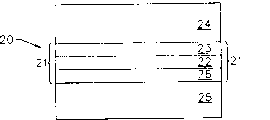
图1是依据本发明的一种过渡结构的原理剖视图;
图2是依据本发明的一种发光二极管的原理剖视图;
图3是另一种发光二极管的剖视原理图;
图4是包含本发明结构的发光二极管的第三种实施方式;
图5是依据本发明及所示组分给出的一种过渡晶体结构的一个二次离子质谱仪(SIMS)的深度分布;
图6是对本发明所述氮化镓外延层使用汞(Hg)接触的差分电容一电压测定法所测出的掺杂浓度与深度的关系曲线图;
图7至图9是不包含本发明的晶体表面的光学显微照片;
图10至图12是包含本发明结构的氮化镓晶体表面的光学显微照片。
本发明是用于在单晶碳化硅和一单晶氮化镓层之间提供优良晶格匹配和热(热膨胀系数)匹配的一种过渡晶体结构。图1示意性地给出了这种过渡结构的剖面图并概括地标以20。这种过渡结构的主要特征是一个用括号标示的缓冲区21。缓冲区由以下两层构成:一个第一氮化镓和氮化铝层22和一个与第一层22邻接的第二氮化镓和氮化铝层23。第二层23中氮化铝的克分子百分比与第一层22中氮化铝的克分子百分比显著不同。
由图1还可看出,过渡结构包括一个位于第二氮化镓和氮化铝层23上的单晶氮化镓层24、一个单晶碳化硅衬底25和一个碳化硅衬底上的氮化铝层26。
最佳实施例中,第一层22中氮化镓的百分比大于该层中氮化铝的克分子百分比。但在第二层23中,氮化铝的克分子百分比大于氮化镓的克分子百分比。虽然为了获得良好的效果,这并不是一种希望的结构,但这种结构的惊人成功之处在于:按通常分析可预料层中氮化镓的克分子百分比越高与纯氮化镓层的匹配越好。而在本发明中,直接与氮化镓外延层24相邻接的是具有较小氮化镓克分子百分比的层23。
图1所示的本结构的最佳实施例中,第一氮化镓和氮化铝层22中氮化铝的克分子百分比近似介于20%和50%之间,氮化铝的最佳克分子百分比约为30%。在第二层23中,氮化铝的克分子百分比近似介于60%和95%之间,最佳值约为90%。
正如本领域熟练人员所知及此处引用的一些参考文献中特别指出的那样,针对这一应用,衬底和任何缓冲层质量度量的一个指标是作出的所需氮化镓层的晶格质量,此处为层24。使用本发明的缓冲区21,形成的氮化镓层中的杂质浓度可低至约1×1016cm-3(参见图6)。
图1还表明在另一实施例中,本发明可以包含垂直器件原始结构,这一结构由一个碳化硅衬底25,衬底25上的缓冲区21和缓冲区上的一个单晶氮化镓层24构成。上面已指出,缓冲区21最好包括三层:碳化硅上的一个氮化铝层26;一个第一氮化镓和氮化铝层22,其中,氮化镓的克分子百分比大于氮化铝的克分子百分比;一个与第一层22邻接的第二氮化镓和氮化铝层23,其中,氮化铝的克分子百分比大于氮化镓的克分子百分比。
缓冲结构的优点以及使用这种缓冲结构制作的前述垂直器件的优点又可以从表示垂直发光二极管的不同实施例的图2、图3和图4中看出。图2示出了一个发光二极管30。二极管30包括一个单晶碳化硅衬底31,一个用括号标示的缓冲区32,一个具有一个第一导电类型的位于缓冲区32上的第一单晶氮化镓层33,一个位于第一层33上的第二单晶氮化镓层34,并具有与第一层相反的导电类型以便第一层33和第二层34之间形成一个p-n结。在衬底31和第二氮化镓层34上作出欧姆接触35和欧姆接触36。
在前一实施例中,过渡区32包括一个位于碳化硅衬底31上的氮化铝外延层37;一个第一氮化镓和氮化铝层40,其中,氮化镓的克分子百分比大于氮化铝的克分子百分比;一个与第一层邻接的第二氮化镓和氮化铝层41,其中,氮化铝的克分子百分比大于氮化镓的克分子百分比。
图2所示的实施例中,缓冲区32未被掺杂并作为一个绝缘层,因而所示的LED 30还包括短路接触42和短路接触43,用于提供一个衬底31和第一单晶氮化镓层33之间的电通路。
图3示出了总括标为45的依据本发明的又一个LED实施例。二极管45包括一个碳化硅衬底46,由平台标示的缓冲区47,一个第一氮化镓层48,一个具有与层48相反导电类型的第二氮化镓层49,以及一个位于氮化镓层48和49间的氮化镓合金层50。合金层50具有与第一氮化镓层同样的导电类型,使得p-n结形成于第二氮化镓层49和氮化镓合金层50之间。本领域将这种结构称为双异质结构,它用来帮助将整个器件中的电流约束在合金层区域以获得更高的效率。衬底46也和第一氮化镓层48具有相同的导电类型。
在最佳实施例中,合金层由铟镓氮(InGaN)组成,使得作成的器件峰值发射波长近似介于410纳米(nm)和470纳米之间。氮化镓也能高效率地发出其它颜色的光,包括绿光(例如470-560nm)。
图3也示出了一组短路接触51和52以及第二氮化镓层和碳化硅衬底46各自的欧姆接触53和54。
图4示出了依据本发明的又一个LED实施例,其中,缓冲区经过了导电性掺杂,因而不再使用短路接触,更准确地说,图4示出的一个二极管60带有一个碳化硅衬底61,用括号62标示出的缓冲结构,第一氮化镓层63,氮化镓合金层64和第二氮化镓层65。与氮化镓层65和碳化硅衬底61的欧姆接触分别示为欧姆接触66和67。与图3的实施例中一样,合金层64与第二氮化镓层65的导电性相反,于是形成了一个p-n结。但合金层64具有与第一GaN层63和SiC衬底61相同的导电性。
由于图4所示器件具有一个导电的缓冲结构,因而不需要图2和图3中给出的短路接触。
在本发明的一些具体例子当中,可厚至6微米的单晶氮化镓层被生长于6H碳化硅衬底上。X射线摆动曲线(θ-2θ扫描)的半宽是54弧秒(arc seconds)。首先可以观察到生长于SiC上光泵激的氮化镓层的受激发射。300K时受激发射的波长为376nm。
一般不是有意地将掺杂层掺杂至浓度约1016cm-3(Nd-Na)。对掺杂的n型层,净杂质浓度控制在1×1017cm-3和4×1018cm-3之间,对P型层,浓度Na-Nd控制在1×1017cm-3和2×1018cm-3之间。蓝色发光二极管使用这些层制作。在电发光光谱中可以观察到波长为375nm的边缘发射,并且在约410nm和470nm之间具有一个峰值。
由于本发明具有少数的晶体缺陷、导电的碳化硅衬底以及所得到的导电碳化硅上的优良氮化镓的组合,从而形成了一种质量极高的氮化镓器件。
碳化硅衬底可按照授予Carter等人的美国专利号4866005的专利文献中所记载的方式生长,而氮化镓、氮化镓合金和缓冲层都另外使用常规化学汽相淀积(CVD)工艺来生长。在CVD外延生长过程中,气流、压力和温度等各种参数虽然在不同系统之间可能并不相同,但对本领域普通技术人员而言,不需过多的试验也可使用其他系统以所述方式生长此处所提到的各种层。
图5是一个SIMS分布图,它进一步表明了本发明的结构特征。其中(从右向左看),扫描显示了硅和碳(即SiC)的存在,接着是铝和氮(AlN)的氮化物,然后是镓、铝和氮(GaN和AlN),最后是镓和氮(GaN)作为顶层。
图6是掺杂浓度与深度的关系曲线,从图中可以看出,本发明使用的碳化硅上生长的氮化镓外延层具有极低的本体杂质浓度(1E16)。
图7、图8和图9是在200倍和400倍之间的倍率拍摄的光学显微照片,如图所示,试图直接在碳化硅上生长氮化镓无法得到所期望的结果。
图10示出了一个氮化镓表面,如图所示,当使用比最优缓冲区稍差的缓冲区时,结果得到轻微的改善。
图11和图12也采用400倍率拍摄,从图中可以看出本发明的优点,特别是GaN晶体表面的相当光滑和无缺陷的晶体结构,与图7至图10相对照更能看出这一点。
通过附图和详细说明,已经公开了本发明的典型最佳实施例,虽然使用了具体的限定,但只用于一般描述性,而不是为了限定,下面的权利要求书将指出本发明的保护范围。
Claims (16)
1.一种过渡晶体结构,用于在单晶的碳化硅和一层单晶的氮化镓之间提供良好的晶格匹配和热匹配,所述过渡晶体结构包括:一个缓冲区,由以下两层构成:
一个第一氮化镓和氮化铝层;
一个与所述的第一层邻接的第二氮化镓和氮化铝层,其中,所述第二层中氮化铝的克分子百分比与所述第一层中氮化铝的克分子百分比显著不同;以及一个位于所述第二氮化镓和氮化铝层上的单晶氮化镓层。
2.根据权利要求1所述的结构,其中所述第一层中氮化镓的克分子百分比大于所述第一层中氮化铝的克分子百分比;以及
其中所述第二层中氮化铝的克分子百分比大于所述第二层中氮化镓的克分子百分比。
3.根据权利要求2所述的结构还包括一个单晶碳化硅衬底;以及
所述缓冲区还包括一个位于所述碳化硅衬底上的氮化铝外延层。
4.根据权利要求3所述的结构,其中,所述第一氮化镓和氮化铝层中氮化铝克分子百分比近似介于20%和50%之间。
5.根据权利要求3所述的结构,其中,所述第一氮化镓和氮化铝层中氮化铝克分子百分比约为30%。
6.根据权利要求3所述的结构,其中,所述第二氮化镓和氮化铝层中氮化铝克分子百分比近似介于60%和95%之间。
7.根据权利要求3所述的结构,其中,所述第二氮化镓和氮化铝层中氮化铝克分子百分比约为90%。
8.根据权利要求3所述的结构,其中,所述衬底选自由6H、4H或者3C多晶型的碳化硅构成的组中。
9.一种由权利要求1所述的过渡晶体结构制作的垂直发光二极管,它还包括:
一个用于所述缓冲区的单晶碳化硅衬底;
具有一个第一导电类型的所述缓冲区中的所述单晶氮化镓层;
一个位于所述单晶氮化镓层上的第二单晶氮化镓层,具有与所述第一导电类型相反的导电类型,所述单晶氮化镓层之间构成一个p-n结;以及
与所述衬底和所述第二氮化镓层的欧姆接触。
10.根据权利要求9所述的发光二极管,其中,所述缓冲区还包括一个位于所述碳化硅衬底上的氮化铝外延层。
11.根据权利要求9所述的发光二极管,其中,所述缓冲区进行了导电性掺杂。
12.根据权利要求9所述的发光二极管,其中,所述缓冲区是一个绝缘层,并且所述二极管还包括所述衬底和所述第一单晶氮化镓层间的短路接触。
13.根据权利要求9所述的发光二极管,它还包括一个位于所述第一和第二氮化镓层间的一个氮化镓合金外延层。
14.根据权利要求13所述的发光二极管,其中,所述氮化镓合金由铟镓氮组成。
15.根据权利要求9所述的发光二极管,峰值发射波长近似位于410纳米和470纳米之间。
16.根据权利要求9所述的发光二极管,峰值发射波长近似位于470纳米和560纳米之间。
Applications Claiming Priority (2)
| Application Number | Priority Date | Filing Date | Title |
|---|---|---|---|
| US08/166,229 | 1993-12-13 | ||
| US08/166,229 US5393993A (en) | 1993-12-13 | 1993-12-13 | Buffer structure between silicon carbide and gallium nitride and resulting semiconductor devices |
Publications (2)
| Publication Number | Publication Date |
|---|---|
| CN1137331A true CN1137331A (zh) | 1996-12-04 |
| CN1059755C CN1059755C (zh) | 2000-12-20 |
Family
ID=22602363
Family Applications (1)
| Application Number | Title | Priority Date | Filing Date |
|---|---|---|---|
| CN94194481A Expired - Lifetime CN1059755C (zh) | 1993-12-13 | 1994-11-01 | 碳化硅与氮化镓间的缓冲结构及由此得到的半导体器件 |
Country Status (11)
| Country | Link |
|---|---|
| US (1) | US5393993A (zh) |
| EP (1) | EP0734593B1 (zh) |
| JP (1) | JP2741705B2 (zh) |
| KR (1) | KR100253026B1 (zh) |
| CN (1) | CN1059755C (zh) |
| AT (1) | ATE176553T1 (zh) |
| AU (1) | AU1300295A (zh) |
| CA (1) | CA2177465C (zh) |
| DE (1) | DE69416427T2 (zh) |
| TW (1) | TW273051B (zh) |
| WO (1) | WO1995017019A1 (zh) |
Cited By (6)
| Publication number | Priority date | Publication date | Assignee | Title |
|---|---|---|---|---|
| CN1132253C (zh) * | 1995-08-31 | 2003-12-24 | 株式会社东芝 | 氮化镓基半导体发光元件及其制造方法 |
| CN1333435C (zh) * | 2004-11-17 | 2007-08-22 | 金芃 | 准氮化铝和准氮化镓基生长衬底及其生长方法 |
| CN100353573C (zh) * | 1996-04-26 | 2007-12-05 | 三洋电机株式会社 | 发光器件的制造方法 |
| CN103258717B (zh) * | 2008-11-27 | 2016-07-06 | 同和电子科技有限公司 | 电子器件用外延基板及其生产方法 |
| CN108091741A (zh) * | 2017-11-15 | 2018-05-29 | 华灿光电(苏州)有限公司 | 一种发光二极管外延片的生长方法 |
| CN112038408A (zh) * | 2020-09-04 | 2020-12-04 | 西安电子科技大学 | 基于碳化硅衬底的垂直氮化铝金属氧化物半导体场效应晶体管及制备方法 |
Families Citing this family (455)
| Publication number | Priority date | Publication date | Assignee | Title |
|---|---|---|---|---|
| DE69431333T2 (de) * | 1993-10-08 | 2003-07-31 | Mitsubishi Cable Industries, Ltd. | GaN-Einkristall |
| JP3325380B2 (ja) | 1994-03-09 | 2002-09-17 | 株式会社東芝 | 半導体発光素子およびその製造方法 |
| US5686737A (en) * | 1994-09-16 | 1997-11-11 | Cree Research, Inc. | Self-aligned field-effect transistor for high frequency applications |
| US5523589A (en) * | 1994-09-20 | 1996-06-04 | Cree Research, Inc. | Vertical geometry light emitting diode with group III nitride active layer and extended lifetime |
| US5631190A (en) * | 1994-10-07 | 1997-05-20 | Cree Research, Inc. | Method for producing high efficiency light-emitting diodes and resulting diode structures |
| US5585648A (en) * | 1995-02-03 | 1996-12-17 | Tischler; Michael A. | High brightness electroluminescent device, emitting in the green to ultraviolet spectrum, and method of making the same |
| US5661074A (en) * | 1995-02-03 | 1997-08-26 | Advanced Technology Materials, Inc. | High brightness electroluminescent device emitting in the green to ultraviolet spectrum and method of making the same |
| US5679965A (en) * | 1995-03-29 | 1997-10-21 | North Carolina State University | Integrated heterostructures of Group III-V nitride semiconductor materials including epitaxial ohmic contact, non-nitride buffer layer and methods of fabricating same |
| US5739554A (en) * | 1995-05-08 | 1998-04-14 | Cree Research, Inc. | Double heterojunction light emitting diode with gallium nitride active layer |
| JP3599896B2 (ja) * | 1995-05-19 | 2004-12-08 | 三洋電機株式会社 | 半導体レーザ素子および半導体レーザ素子の製造方法 |
| US5919422A (en) * | 1995-07-28 | 1999-07-06 | Toyoda Gosei Co., Ltd. | Titanium dioxide photo-catalyzer |
| US5923058A (en) * | 1995-11-09 | 1999-07-13 | Northrop Grumman Corporation | Aluminum gallium nitride heterojunction bipolar transistor |
| US5915164A (en) * | 1995-12-28 | 1999-06-22 | U.S. Philips Corporation | Methods of making high voltage GaN-A1N based semiconductor devices |
| ES2169712T3 (es) * | 1995-12-29 | 2003-10-16 | Cree Inc | Visualizador de matriz de led dde diferentes colores y tensiones. |
| US5812105A (en) * | 1996-06-10 | 1998-09-22 | Cree Research, Inc. | Led dot matrix drive method and apparatus |
| US7385574B1 (en) | 1995-12-29 | 2008-06-10 | Cree, Inc. | True color flat panel display module |
| US5874747A (en) * | 1996-02-05 | 1999-02-23 | Advanced Technology Materials, Inc. | High brightness electroluminescent device emitting in the green to ultraviolet spectrum and method of making the same |
| US5763905A (en) * | 1996-07-09 | 1998-06-09 | Abb Research Ltd. | Semiconductor device having a passivation layer |
| US6533874B1 (en) * | 1996-12-03 | 2003-03-18 | Advanced Technology Materials, Inc. | GaN-based devices using thick (Ga, Al, In)N base layers |
| US6284395B1 (en) | 1997-03-05 | 2001-09-04 | Corning Applied Technologies Corp. | Nitride based semiconductors and devices |
| US5923946A (en) * | 1997-04-17 | 1999-07-13 | Cree Research, Inc. | Recovery of surface-ready silicon carbide substrates |
| JP3957359B2 (ja) * | 1997-05-21 | 2007-08-15 | シャープ株式会社 | 窒化ガリウム系化合物半導体発光素子及びその製造方法 |
| JP3822318B2 (ja) * | 1997-07-17 | 2006-09-20 | 株式会社東芝 | 半導体発光素子及びその製造方法 |
| AU747260B2 (en) | 1997-07-25 | 2002-05-09 | Nichia Chemical Industries, Ltd. | Nitride semiconductor device |
| AU9295098A (en) * | 1997-08-29 | 1999-03-16 | Cree Research, Inc. | Robust group iii light emitting diode for high reliability in standard packagingapplications |
| US6825501B2 (en) * | 1997-08-29 | 2004-11-30 | Cree, Inc. | Robust Group III light emitting diode for high reliability in standard packaging applications |
| US6201262B1 (en) | 1997-10-07 | 2001-03-13 | Cree, Inc. | Group III nitride photonic devices on silicon carbide substrates with conductive buffer interlay structure |
| US6599133B2 (en) | 1997-11-18 | 2003-07-29 | Technologies And Devices International, Inc. | Method for growing III-V compound semiconductor structures with an integral non-continuous quantum dot layer utilizing HVPE techniques |
| US6559038B2 (en) | 1997-11-18 | 2003-05-06 | Technologies And Devices International, Inc. | Method for growing p-n heterojunction-based structures utilizing HVPE techniques |
| US20020047135A1 (en) * | 1997-11-18 | 2002-04-25 | Nikolaev Audrey E. | P-N junction-based structures utilizing HVPE grown III-V compound layers |
| US6218269B1 (en) | 1997-11-18 | 2001-04-17 | Technology And Devices International, Inc. | Process for producing III-V nitride pn junctions and p-i-n junctions |
| US6472300B2 (en) | 1997-11-18 | 2002-10-29 | Technologies And Devices International, Inc. | Method for growing p-n homojunction-based structures utilizing HVPE techniques |
| US6476420B2 (en) | 1997-11-18 | 2002-11-05 | Technologies And Devices International, Inc. | P-N homojunction-based structures utilizing HVPE growth III-V compound layers |
| US6559467B2 (en) | 1997-11-18 | 2003-05-06 | Technologies And Devices International, Inc. | P-n heterojunction-based structures utilizing HVPE grown III-V compound layers |
| US6890809B2 (en) * | 1997-11-18 | 2005-05-10 | Technologies And Deviles International, Inc. | Method for fabricating a P-N heterojunction device utilizing HVPE grown III-V compound layers and resultant device |
| US6555452B2 (en) | 1997-11-18 | 2003-04-29 | Technologies And Devices International, Inc. | Method for growing p-type III-V compound material utilizing HVPE techniques |
| US6479839B2 (en) | 1997-11-18 | 2002-11-12 | Technologies & Devices International, Inc. | III-V compounds semiconductor device with an AlxByInzGa1-x-y-zN non continuous quantum dot layer |
| US6849862B2 (en) * | 1997-11-18 | 2005-02-01 | Technologies And Devices International, Inc. | III-V compound semiconductor device with an AlxByInzGa1-x-y-zN1-a-bPaAsb non-continuous quantum dot layer |
| JP4166885B2 (ja) * | 1998-05-18 | 2008-10-15 | 富士通株式会社 | 光半導体装置およびその製造方法 |
| KR100304881B1 (ko) * | 1998-10-15 | 2001-10-12 | 구자홍 | Gan계화합물반도체및그의결정성장방법 |
| DE19904378B4 (de) | 1999-02-03 | 2006-10-05 | Osram Opto Semiconductors Gmbh | Verfahren zur Herstellung von Nitrid-Einkristallen |
| US6326654B1 (en) * | 1999-02-05 | 2001-12-04 | The United States Of America As Represented By The Secretary Of The Air Force | Hybrid ultraviolet detector |
| JP3770014B2 (ja) | 1999-02-09 | 2006-04-26 | 日亜化学工業株式会社 | 窒化物半導体素子 |
| ATE452445T1 (de) | 1999-03-04 | 2010-01-15 | Nichia Corp | Nitridhalbleiterlaserelement |
| US8090619B1 (en) | 1999-08-27 | 2012-01-03 | Ochoa Optics Llc | Method and system for music distribution |
| US7209900B2 (en) * | 1999-08-27 | 2007-04-24 | Charles Eric Hunter | Music distribution systems |
| US7647618B1 (en) * | 1999-08-27 | 2010-01-12 | Charles Eric Hunter | Video distribution system |
| US8656423B2 (en) * | 1999-08-27 | 2014-02-18 | Ochoa Optics Llc | Video distribution system |
| US8829546B2 (en) | 1999-11-19 | 2014-09-09 | Cree, Inc. | Rare earth doped layer or substrate for light conversion |
| US9252898B2 (en) * | 2000-01-28 | 2016-02-02 | Zarbaña Digital Fund Llc | Music distribution systems |
| JP2001217456A (ja) * | 2000-02-03 | 2001-08-10 | Sharp Corp | 窒化ガリウム系化合物半導体発光素子 |
| US6495894B2 (en) * | 2000-05-22 | 2002-12-17 | Ngk Insulators, Ltd. | Photonic device, a substrate for fabricating a photonic device, a method for fabricating the photonic device and a method for manufacturing the photonic device-fabricating substrate |
| AU2001279163A1 (en) * | 2000-08-04 | 2002-02-18 | The Regents Of The University Of California | Method of controlling stress in gallium nitride films deposited on substrates |
| US6525464B1 (en) * | 2000-09-08 | 2003-02-25 | Unity Opto Technology Co., Ltd. | Stacked light-mixing LED |
| US6787010B2 (en) | 2000-11-30 | 2004-09-07 | North Carolina State University | Non-thermionic sputter material transport device, methods of use, and materials produced thereby |
| EP1346085B1 (en) | 2000-11-30 | 2011-10-12 | North Carolina State University | Method for producing group iii metal nitride based materials |
| US6649287B2 (en) | 2000-12-14 | 2003-11-18 | Nitronex Corporation | Gallium nitride materials and methods |
| US6657237B2 (en) * | 2000-12-18 | 2003-12-02 | Samsung Electro-Mechanics Co., Ltd. | GaN based group III-V nitride semiconductor light-emitting diode and method for fabricating the same |
| US6906352B2 (en) | 2001-01-16 | 2005-06-14 | Cree, Inc. | Group III nitride LED with undoped cladding layer and multiple quantum well |
| US6800876B2 (en) | 2001-01-16 | 2004-10-05 | Cree, Inc. | Group III nitride LED with undoped cladding layer (5000.137) |
| US6794684B2 (en) | 2001-02-01 | 2004-09-21 | Cree, Inc. | Reflective ohmic contacts for silicon carbide including a layer consisting essentially of nickel, methods of fabricating same, and light emitting devices including the same |
| US6791119B2 (en) * | 2001-02-01 | 2004-09-14 | Cree, Inc. | Light emitting diodes including modifications for light extraction |
| US6611002B2 (en) | 2001-02-23 | 2003-08-26 | Nitronex Corporation | Gallium nitride material devices and methods including backside vias |
| US7233028B2 (en) * | 2001-02-23 | 2007-06-19 | Nitronex Corporation | Gallium nitride material devices and methods of forming the same |
| US6956250B2 (en) | 2001-02-23 | 2005-10-18 | Nitronex Corporation | Gallium nitride materials including thermally conductive regions |
| US6576932B2 (en) | 2001-03-01 | 2003-06-10 | Lumileds Lighting, U.S., Llc | Increasing the brightness of III-nitride light emitting devices |
| US6958497B2 (en) | 2001-05-30 | 2005-10-25 | Cree, Inc. | Group III nitride based light emitting diode structures with a quantum well and superlattice, group III nitride based quantum well structures and group III nitride based superlattice structures |
| US7692182B2 (en) | 2001-05-30 | 2010-04-06 | Cree, Inc. | Group III nitride based quantum well light emitting device structures with an indium containing capping structure |
| CN101834245B (zh) | 2001-06-15 | 2013-05-22 | 克里公司 | 在SiC衬底上形成的GaN基LED |
| US6747298B2 (en) * | 2001-07-23 | 2004-06-08 | Cree, Inc. | Collets for bonding of light emitting diodes having shaped substrates |
| US6888167B2 (en) | 2001-07-23 | 2005-05-03 | Cree, Inc. | Flip-chip bonding of light emitting devices and light emitting devices suitable for flip-chip bonding |
| US6740906B2 (en) * | 2001-07-23 | 2004-05-25 | Cree, Inc. | Light emitting diodes including modifications for submount bonding |
| US7211833B2 (en) | 2001-07-23 | 2007-05-01 | Cree, Inc. | Light emitting diodes including barrier layers/sublayers |
| US7960005B2 (en) | 2001-09-14 | 2011-06-14 | Ochoa Optics Llc | Broadcast distribution of content for storage on hardware protected optical storage media |
| US7858403B2 (en) | 2001-10-31 | 2010-12-28 | Cree, Inc. | Methods and systems for fabricating broad spectrum light emitting devices |
| US20030090103A1 (en) * | 2001-11-09 | 2003-05-15 | Thomas Becker | Direct mailing device |
| US6683327B2 (en) | 2001-11-13 | 2004-01-27 | Lumileds Lighting U.S., Llc | Nucleation layer for improved light extraction from light emitting devices |
| US7030428B2 (en) * | 2001-12-03 | 2006-04-18 | Cree, Inc. | Strain balanced nitride heterojunction transistors |
| US6635503B2 (en) | 2002-01-28 | 2003-10-21 | Cree, Inc. | Cluster packaging of light emitting diodes |
| WO2003073514A1 (en) * | 2002-02-28 | 2003-09-04 | The Furukawa Electric Co., Ltd. | Group iii-v nitride semiconductor multilayer structure and its production process |
| KR100460332B1 (ko) * | 2002-05-23 | 2004-12-08 | 박정희 | 실리콘 카바이드 나노선의 제조방법 |
| KR101030068B1 (ko) * | 2002-07-08 | 2011-04-19 | 니치아 카가쿠 고교 가부시키가이샤 | 질화물 반도체 소자의 제조방법 및 질화물 반도체 소자 |
| US6982204B2 (en) * | 2002-07-16 | 2006-01-03 | Cree, Inc. | Nitride-based transistors and methods of fabrication thereof using non-etched contact recesses |
| US6841001B2 (en) | 2002-07-19 | 2005-01-11 | Cree, Inc. | Strain compensated semiconductor structures and methods of fabricating strain compensated semiconductor structures |
| US6875995B2 (en) * | 2002-08-16 | 2005-04-05 | Cree, Inc. | Heterogeneous bandgap structures for semiconductor devices and manufacturing methods therefor |
| US10340424B2 (en) | 2002-08-30 | 2019-07-02 | GE Lighting Solutions, LLC | Light emitting diode component |
| EP1540747B1 (en) * | 2002-09-19 | 2012-01-25 | Cree, Inc. | Phosphor-coated light emitting diodes including tapered sidewalls, and fabrication methods therefor |
| US7009199B2 (en) * | 2002-10-22 | 2006-03-07 | Cree, Inc. | Electronic devices having a header and antiparallel connected light emitting diodes for producing light from AC current |
| US6900067B2 (en) * | 2002-12-11 | 2005-05-31 | Lumileds Lighting U.S., Llc | Growth of III-nitride films on mismatched substrates without conventional low temperature nucleation layers |
| US6952024B2 (en) * | 2003-02-13 | 2005-10-04 | Cree, Inc. | Group III nitride LED with silicon carbide cladding layer |
| US7170097B2 (en) * | 2003-02-14 | 2007-01-30 | Cree, Inc. | Inverted light emitting diode on conductive substrate |
| GB2398672A (en) | 2003-02-19 | 2004-08-25 | Qinetiq Ltd | Group IIIA nitride buffer layers |
| US7112860B2 (en) * | 2003-03-03 | 2006-09-26 | Cree, Inc. | Integrated nitride-based acoustic wave devices and methods of fabricating integrated nitride-based acoustic wave devices |
| US7898047B2 (en) | 2003-03-03 | 2011-03-01 | Samsung Electronics Co., Ltd. | Integrated nitride and silicon carbide-based devices and methods of fabricating integrated nitride-based devices |
| US6885033B2 (en) * | 2003-03-10 | 2005-04-26 | Cree, Inc. | Light emitting devices for light conversion and methods and semiconductor chips for fabricating the same |
| US7531380B2 (en) | 2003-04-30 | 2009-05-12 | Cree, Inc. | Methods of forming light-emitting devices having an active region with electrical contacts coupled to opposing surfaces thereof |
| US7087936B2 (en) * | 2003-04-30 | 2006-08-08 | Cree, Inc. | Methods of forming light-emitting devices having an antireflective layer that has a graded index of refraction |
| US7714345B2 (en) * | 2003-04-30 | 2010-05-11 | Cree, Inc. | Light-emitting devices having coplanar electrical contacts adjacent to a substrate surface opposite an active region and methods of forming the same |
| US7338822B2 (en) * | 2003-05-09 | 2008-03-04 | Cree, Inc. | LED fabrication via ion implant isolation |
| US7135720B2 (en) * | 2003-08-05 | 2006-11-14 | Nitronex Corporation | Gallium nitride material transistors and methods associated with the same |
| US20050104072A1 (en) | 2003-08-14 | 2005-05-19 | Slater David B.Jr. | Localized annealing of metal-silicon carbide ohmic contacts and devices so formed |
| US7183587B2 (en) * | 2003-09-09 | 2007-02-27 | Cree, Inc. | Solid metal block mounting substrates for semiconductor light emitting devices |
| US7029935B2 (en) * | 2003-09-09 | 2006-04-18 | Cree, Inc. | Transmissive optical elements including transparent plastic shell having a phosphor dispersed therein, and methods of fabricating same |
| WO2005024909A2 (en) * | 2003-09-09 | 2005-03-17 | The Regents Of The University Of California | Fabrication of single or multiple gate field plates |
| US7501669B2 (en) | 2003-09-09 | 2009-03-10 | Cree, Inc. | Wide bandgap transistor devices with field plates |
| US7915085B2 (en) * | 2003-09-18 | 2011-03-29 | Cree, Inc. | Molded chip fabrication method |
| KR20060131774A (ko) * | 2003-11-12 | 2006-12-20 | 크리 인코포레이티드 | 반도체 웨이퍼 후면들 상에 발광 소자들을 가지는 상기반도체 웨이퍼 후면들의 가공 방법들 및 상기 방법들에의해 형성된 발광 소자들 |
| US20050194584A1 (en) * | 2003-11-12 | 2005-09-08 | Slater David B.Jr. | LED fabrication via ion implant isolation |
| JP4525894B2 (ja) * | 2003-11-21 | 2010-08-18 | サンケン電気株式会社 | 半導体素子形成用板状基体及びこの製造方法及びこれを使用した半導体素子 |
| US7518158B2 (en) * | 2003-12-09 | 2009-04-14 | Cree, Inc. | Semiconductor light emitting devices and submounts |
| US7071498B2 (en) * | 2003-12-17 | 2006-07-04 | Nitronex Corporation | Gallium nitride material devices including an electrode-defining layer and methods of forming the same |
| US20050145851A1 (en) * | 2003-12-17 | 2005-07-07 | Nitronex Corporation | Gallium nitride material structures including isolation regions and methods |
| US7135715B2 (en) * | 2004-01-07 | 2006-11-14 | Cree, Inc. | Co-doping for fermi level control in semi-insulating Group III nitrides |
| US7045404B2 (en) * | 2004-01-16 | 2006-05-16 | Cree, Inc. | Nitride-based transistors with a protective layer and a low-damage recess and methods of fabrication thereof |
| US7901994B2 (en) * | 2004-01-16 | 2011-03-08 | Cree, Inc. | Methods of manufacturing group III nitride semiconductor devices with silicon nitride layers |
| US7033912B2 (en) | 2004-01-22 | 2006-04-25 | Cree, Inc. | Silicon carbide on diamond substrates and related devices and methods |
| US7612390B2 (en) * | 2004-02-05 | 2009-11-03 | Cree, Inc. | Heterojunction transistors including energy barriers |
| US7170111B2 (en) * | 2004-02-05 | 2007-01-30 | Cree, Inc. | Nitride heterojunction transistors having charge-transfer induced energy barriers and methods of fabricating the same |
| US7615689B2 (en) * | 2004-02-12 | 2009-11-10 | Seminis Vegatable Seeds, Inc. | Methods for coupling resistance alleles in tomato |
| US7202181B2 (en) * | 2004-03-26 | 2007-04-10 | Cres, Inc. | Etching of substrates of light emitting devices |
| US7355284B2 (en) | 2004-03-29 | 2008-04-08 | Cree, Inc. | Semiconductor light emitting devices including flexible film having therein an optical element |
| US7439609B2 (en) * | 2004-03-29 | 2008-10-21 | Cree, Inc. | Doping of gallium nitride by solid source diffusion and resulting gallium nitride structures |
| US7279346B2 (en) * | 2004-03-31 | 2007-10-09 | Cree, Inc. | Method for packaging a light emitting device by one dispense then cure step followed by another |
| US7517728B2 (en) * | 2004-03-31 | 2009-04-14 | Cree, Inc. | Semiconductor light emitting devices including a luminescent conversion element |
| US7326583B2 (en) | 2004-03-31 | 2008-02-05 | Cree, Inc. | Methods for packaging of a semiconductor light emitting device |
| US7419912B2 (en) * | 2004-04-01 | 2008-09-02 | Cree, Inc. | Laser patterning of light emitting devices |
| US7868343B2 (en) * | 2004-04-06 | 2011-01-11 | Cree, Inc. | Light-emitting devices having multiple encapsulation layers with at least one of the encapsulation layers including nanoparticles and methods of forming the same |
| WO2005106985A2 (en) | 2004-04-22 | 2005-11-10 | Cree, Inc. | Improved substrate buffer structure for group iii nitride devices |
| US7592634B2 (en) * | 2004-05-06 | 2009-09-22 | Cree, Inc. | LED fabrication via ion implant isolation |
| US7550783B2 (en) | 2004-05-11 | 2009-06-23 | Cree, Inc. | Wide bandgap HEMTs with source connected field plates |
| US7573078B2 (en) | 2004-05-11 | 2009-08-11 | Cree, Inc. | Wide bandgap transistors with multiple field plates |
| US9773877B2 (en) | 2004-05-13 | 2017-09-26 | Cree, Inc. | Wide bandgap field effect transistors with source connected field plates |
| US7432142B2 (en) * | 2004-05-20 | 2008-10-07 | Cree, Inc. | Methods of fabricating nitride-based transistors having regrown ohmic contact regions |
| US7084441B2 (en) * | 2004-05-20 | 2006-08-01 | Cree, Inc. | Semiconductor devices having a hybrid channel layer, current aperture transistors and methods of fabricating same |
| US7361946B2 (en) * | 2004-06-28 | 2008-04-22 | Nitronex Corporation | Semiconductor device-based sensors |
| US7339205B2 (en) * | 2004-06-28 | 2008-03-04 | Nitronex Corporation | Gallium nitride materials and methods associated with the same |
| WO2006005062A2 (en) * | 2004-06-30 | 2006-01-12 | Cree, Inc. | Chip-scale methods for packaging light emitting devices and chip-scale packaged light emitting devices |
| US20060002442A1 (en) * | 2004-06-30 | 2006-01-05 | Kevin Haberern | Light emitting devices having current blocking structures and methods of fabricating light emitting devices having current blocking structures |
| US7795623B2 (en) | 2004-06-30 | 2010-09-14 | Cree, Inc. | Light emitting devices having current reducing structures and methods of forming light emitting devices having current reducing structures |
| US7687827B2 (en) * | 2004-07-07 | 2010-03-30 | Nitronex Corporation | III-nitride materials including low dislocation densities and methods associated with the same |
| US7238560B2 (en) | 2004-07-23 | 2007-07-03 | Cree, Inc. | Methods of fabricating nitride-based transistors with a cap layer and a recessed gate |
| US7118262B2 (en) * | 2004-07-23 | 2006-10-10 | Cree, Inc. | Reflective optical elements for semiconductor light emitting devices |
| US20060017064A1 (en) * | 2004-07-26 | 2006-01-26 | Saxler Adam W | Nitride-based transistors having laterally grown active region and methods of fabricating same |
| TWI374552B (en) * | 2004-07-27 | 2012-10-11 | Cree Inc | Ultra-thin ohmic contacts for p-type nitride light emitting devices and methods of forming |
| US7557380B2 (en) | 2004-07-27 | 2009-07-07 | Cree, Inc. | Light emitting devices having a reflective bond pad and methods of fabricating light emitting devices having reflective bond pads |
| US7217583B2 (en) * | 2004-09-21 | 2007-05-15 | Cree, Inc. | Methods of coating semiconductor light emitting elements by evaporating solvent from a suspension |
| US7294324B2 (en) * | 2004-09-21 | 2007-11-13 | Cree, Inc. | Low basal plane dislocation bulk grown SiC wafers |
| US7372198B2 (en) | 2004-09-23 | 2008-05-13 | Cree, Inc. | Semiconductor light emitting devices including patternable films comprising transparent silicone and phosphor |
| US20060097385A1 (en) * | 2004-10-25 | 2006-05-11 | Negley Gerald H | Solid metal block semiconductor light emitting device mounting substrates and packages including cavities and heat sinks, and methods of packaging same |
| EP1831919A2 (en) * | 2004-10-28 | 2007-09-12 | Nitronex Corporation | Gallium nitride/silicon based monolithic microwave integrated circuit |
| US7709859B2 (en) * | 2004-11-23 | 2010-05-04 | Cree, Inc. | Cap layers including aluminum nitride for nitride-based transistors |
| US7456443B2 (en) | 2004-11-23 | 2008-11-25 | Cree, Inc. | Transistors having buried n-type and p-type regions beneath the source region |
| US7247889B2 (en) | 2004-12-03 | 2007-07-24 | Nitronex Corporation | III-nitride material structures including silicon substrates |
| US7355215B2 (en) * | 2004-12-06 | 2008-04-08 | Cree, Inc. | Field effect transistors (FETs) having multi-watt output power at millimeter-wave frequencies |
| US7161194B2 (en) * | 2004-12-06 | 2007-01-09 | Cree, Inc. | High power density and/or linearity transistors |
| US7322732B2 (en) | 2004-12-23 | 2008-01-29 | Cree, Inc. | Light emitting diode arrays for direct backlighting of liquid crystal displays |
| US7236053B2 (en) | 2004-12-31 | 2007-06-26 | Cree, Inc. | High efficiency switch-mode power amplifier |
| US8125137B2 (en) | 2005-01-10 | 2012-02-28 | Cree, Inc. | Multi-chip light emitting device lamps for providing high-CRI warm white light and light fixtures including the same |
| US7304694B2 (en) * | 2005-01-12 | 2007-12-04 | Cree, Inc. | Solid colloidal dispersions for backlighting of liquid crystal displays |
| US7335920B2 (en) * | 2005-01-24 | 2008-02-26 | Cree, Inc. | LED with current confinement structure and surface roughening |
| US7939842B2 (en) * | 2005-01-27 | 2011-05-10 | Cree, Inc. | Light emitting device packages, light emitting diode (LED) packages and related methods |
| US7465967B2 (en) * | 2005-03-15 | 2008-12-16 | Cree, Inc. | Group III nitride field effect transistors (FETS) capable of withstanding high temperature reverse bias test conditions |
| US7422634B2 (en) * | 2005-04-07 | 2008-09-09 | Cree, Inc. | Three inch silicon carbide wafer with low warp, bow, and TTV |
| US7626217B2 (en) * | 2005-04-11 | 2009-12-01 | Cree, Inc. | Composite substrates of conductive and insulating or semi-insulating group III-nitrides for group III-nitride devices |
| US8575651B2 (en) | 2005-04-11 | 2013-11-05 | Cree, Inc. | Devices having thick semi-insulating epitaxial gallium nitride layer |
| US7544963B2 (en) * | 2005-04-29 | 2009-06-09 | Cree, Inc. | Binary group III-nitride based high electron mobility transistors |
| US7615774B2 (en) * | 2005-04-29 | 2009-11-10 | Cree.Inc. | Aluminum free group III-nitride based high electron mobility transistors |
| US7446345B2 (en) * | 2005-04-29 | 2008-11-04 | Cree, Inc. | Light emitting devices with active layers that extend into opened pits |
| US7365374B2 (en) * | 2005-05-03 | 2008-04-29 | Nitronex Corporation | Gallium nitride material structures including substrates and methods associated with the same |
| US20060267043A1 (en) * | 2005-05-27 | 2006-11-30 | Emerson David T | Deep ultraviolet light emitting devices and methods of fabricating deep ultraviolet light emitting devices |
| US9331192B2 (en) * | 2005-06-29 | 2016-05-03 | Cree, Inc. | Low dislocation density group III nitride layers on silicon carbide substrates and methods of making the same |
| TWI422044B (zh) * | 2005-06-30 | 2014-01-01 | 克立公司 | 封裝發光裝置之晶片尺度方法及經晶片尺度封裝之發光裝置 |
| US20070018199A1 (en) * | 2005-07-20 | 2007-01-25 | Cree, Inc. | Nitride-based transistors and fabrication methods with an etch stop layer |
| US20070018198A1 (en) * | 2005-07-20 | 2007-01-25 | Brandes George R | High electron mobility electronic device structures comprising native substrates and methods for making the same |
| US7646035B2 (en) * | 2006-05-31 | 2010-01-12 | Cree, Inc. | Packaged light emitting devices including multiple index lenses and multiple index lenses for packaged light emitting devices |
| US7365371B2 (en) * | 2005-08-04 | 2008-04-29 | Cree, Inc. | Packages for semiconductor light emitting devices utilizing dispensed encapsulants |
| US8835952B2 (en) | 2005-08-04 | 2014-09-16 | Cree, Inc. | Submounts for semiconductor light emitting devices and methods of forming packaged light emitting devices including dispensed encapsulants |
| EP2312634B1 (en) | 2005-09-07 | 2019-12-25 | Cree, Inc. | Transistors with fluorine treatment |
| WO2007041710A2 (en) * | 2005-10-04 | 2007-04-12 | Nitronex Corporation | Gallium nitride material transistors and methods for wideband applications |
| US7566913B2 (en) | 2005-12-02 | 2009-07-28 | Nitronex Corporation | Gallium nitride material devices including conductive regions and methods associated with the same |
| WO2007064689A1 (en) | 2005-12-02 | 2007-06-07 | Nitronex Corporation | Gallium nitride material devices and associated methods |
| US7419892B2 (en) * | 2005-12-13 | 2008-09-02 | Cree, Inc. | Semiconductor devices including implanted regions and protective layers and methods of forming the same |
| JP5614766B2 (ja) * | 2005-12-21 | 2014-10-29 | クリー インコーポレイテッドCree Inc. | 照明装置 |
| CN101351891B (zh) * | 2005-12-22 | 2014-11-19 | 科锐公司 | 照明装置 |
| US7592211B2 (en) | 2006-01-17 | 2009-09-22 | Cree, Inc. | Methods of fabricating transistors including supported gate electrodes |
| US7709269B2 (en) * | 2006-01-17 | 2010-05-04 | Cree, Inc. | Methods of fabricating transistors including dielectrically-supported gate electrodes |
| US7442564B2 (en) * | 2006-01-19 | 2008-10-28 | Cree, Inc. | Dispensed electrical interconnections |
| US8441179B2 (en) | 2006-01-20 | 2013-05-14 | Cree, Inc. | Lighting devices having remote lumiphors that are excited by lumiphor-converted semiconductor excitation sources |
| US7521728B2 (en) * | 2006-01-20 | 2009-04-21 | Cree, Inc. | Packages for semiconductor light emitting devices utilizing dispensed reflectors and methods of forming the same |
| JP2009524247A (ja) * | 2006-01-20 | 2009-06-25 | クリー エル イー ディー ライティング ソリューションズ インコーポレイテッド | ルミファー膜を空間的に分離することにより固体光発光素子におけるスペクトル内容をシフトすること |
| US8101961B2 (en) * | 2006-01-25 | 2012-01-24 | Cree, Inc. | Transparent ohmic contacts on light emitting diodes with growth substrates |
| US7566918B2 (en) * | 2006-02-23 | 2009-07-28 | Cree, Inc. | Nitride based transistors for millimeter wave operation |
| KR101198763B1 (ko) * | 2006-03-23 | 2012-11-12 | 엘지이노텍 주식회사 | 기둥 구조와 이를 이용한 발광 소자 및 그 형성방법 |
| US7388236B2 (en) * | 2006-03-29 | 2008-06-17 | Cree, Inc. | High efficiency and/or high power density wide bandgap transistors |
| US8969908B2 (en) * | 2006-04-04 | 2015-03-03 | Cree, Inc. | Uniform emission LED package |
| US8373195B2 (en) | 2006-04-12 | 2013-02-12 | SemiLEDs Optoelectronics Co., Ltd. | Light-emitting diode lamp with low thermal resistance |
| US7863639B2 (en) * | 2006-04-12 | 2011-01-04 | Semileds Optoelectronics Co. Ltd. | Light-emitting diode lamp with low thermal resistance |
| US9040398B2 (en) * | 2006-05-16 | 2015-05-26 | Cree, Inc. | Method of fabricating seminconductor devices including self aligned refractory contacts |
| US8033692B2 (en) * | 2006-05-23 | 2011-10-11 | Cree, Inc. | Lighting device |
| WO2007139780A2 (en) * | 2006-05-23 | 2007-12-06 | Cree Led Lighting Solutions, Inc. | Lighting device and method of making |
| JP2009538536A (ja) | 2006-05-26 | 2009-11-05 | クリー エル イー ディー ライティング ソリューションズ インコーポレイテッド | 固体発光デバイス、および、それを製造する方法 |
| US8698184B2 (en) | 2011-01-21 | 2014-04-15 | Cree, Inc. | Light emitting diodes with low junction temperature and solid state backlight components including light emitting diodes with low junction temperature |
| US7943952B2 (en) * | 2006-07-31 | 2011-05-17 | Cree, Inc. | Method of uniform phosphor chip coating and LED package fabricated using method |
| US8432012B2 (en) | 2006-08-01 | 2013-04-30 | Cree, Inc. | Semiconductor devices including schottky diodes having overlapping doped regions and methods of fabricating same |
| US7728402B2 (en) * | 2006-08-01 | 2010-06-01 | Cree, Inc. | Semiconductor devices including schottky diodes with controlled breakdown |
| US20080035143A1 (en) * | 2006-08-14 | 2008-02-14 | Sievers Robert E | Human-powered dry powder inhaler and dry powder inhaler compositions |
| EP2631951B1 (en) * | 2006-08-17 | 2017-10-11 | Cree, Inc. | High power insulated gate bipolar transistors |
| US7646024B2 (en) * | 2006-08-18 | 2010-01-12 | Cree, Inc. | Structure and method for reducing forward voltage across a silicon carbide-group III nitride interface |
| US7763478B2 (en) | 2006-08-21 | 2010-07-27 | Cree, Inc. | Methods of forming semiconductor light emitting device packages by liquid injection molding |
| US8310143B2 (en) | 2006-08-23 | 2012-11-13 | Cree, Inc. | Lighting device and lighting method |
| US7808013B2 (en) * | 2006-10-31 | 2010-10-05 | Cree, Inc. | Integrated heat spreaders for light emitting devices (LEDs) and related assemblies |
| US8823057B2 (en) | 2006-11-06 | 2014-09-02 | Cree, Inc. | Semiconductor devices including implanted regions for providing low-resistance contact to buried layers and related devices |
| US10295147B2 (en) * | 2006-11-09 | 2019-05-21 | Cree, Inc. | LED array and method for fabricating same |
| JP5105160B2 (ja) | 2006-11-13 | 2012-12-19 | クリー インコーポレイテッド | トランジスタ |
| US7692263B2 (en) | 2006-11-21 | 2010-04-06 | Cree, Inc. | High voltage GaN transistors |
| US9318327B2 (en) | 2006-11-28 | 2016-04-19 | Cree, Inc. | Semiconductor devices having low threading dislocations and improved light extraction and methods of making the same |
| WO2008091837A2 (en) * | 2007-01-22 | 2008-07-31 | Cree Led Lighting Solutions, Inc. | Fault tolerant light emitters, systems incorporating fault tolerant light emitters and methods of fabricating fault tolerant light emitters |
| US9159888B2 (en) * | 2007-01-22 | 2015-10-13 | Cree, Inc. | Wafer level phosphor coating method and devices fabricated utilizing method |
| US8232564B2 (en) * | 2007-01-22 | 2012-07-31 | Cree, Inc. | Wafer level phosphor coating technique for warm light emitting diodes |
| TWI440210B (zh) | 2007-01-22 | 2014-06-01 | 克里公司 | 使用發光裝置外部互連陣列之照明裝置及其製造方法 |
| US9024349B2 (en) * | 2007-01-22 | 2015-05-05 | Cree, Inc. | Wafer level phosphor coating method and devices fabricated utilizing method |
| US9061450B2 (en) * | 2007-02-12 | 2015-06-23 | Cree, Inc. | Methods of forming packaged semiconductor light emitting devices having front contacts by compression molding |
| US7709853B2 (en) * | 2007-02-12 | 2010-05-04 | Cree, Inc. | Packaged semiconductor light emitting devices having multiple optical elements |
| US20080198572A1 (en) * | 2007-02-21 | 2008-08-21 | Medendorp Nicholas W | LED lighting systems including luminescent layers on remote reflectors |
| US8835987B2 (en) | 2007-02-27 | 2014-09-16 | Cree, Inc. | Insulated gate bipolar transistors including current suppressing layers |
| US8362503B2 (en) | 2007-03-09 | 2013-01-29 | Cree, Inc. | Thick nitride semiconductor structures with interlayer structures |
| US7825432B2 (en) | 2007-03-09 | 2010-11-02 | Cree, Inc. | Nitride semiconductor structures with interlayer structures |
| US9484499B2 (en) * | 2007-04-20 | 2016-11-01 | Cree, Inc. | Transparent ohmic contacts on light emitting diodes with carrier substrates |
| US7910944B2 (en) | 2007-05-04 | 2011-03-22 | Cree, Inc. | Side mountable semiconductor light emitting device packages and panels |
| US7982363B2 (en) * | 2007-05-14 | 2011-07-19 | Cree, Inc. | Bulk acoustic device and method for fabricating |
| US20090002979A1 (en) * | 2007-06-27 | 2009-01-01 | Cree, Inc. | Light emitting device (led) lighting systems for emitting light in multiple directions and related methods |
| US8042971B2 (en) * | 2007-06-27 | 2011-10-25 | Cree, Inc. | Light emitting device (LED) lighting systems for emitting light in multiple directions and related methods |
| US10505083B2 (en) * | 2007-07-11 | 2019-12-10 | Cree, Inc. | Coating method utilizing phosphor containment structure and devices fabricated using same |
| EP2171502B1 (en) * | 2007-07-17 | 2016-09-14 | Cree, Inc. | Optical elements with internal optical features and methods of fabricating same |
| US7863635B2 (en) * | 2007-08-07 | 2011-01-04 | Cree, Inc. | Semiconductor light emitting devices with applied wavelength conversion materials |
| US20090039375A1 (en) * | 2007-08-07 | 2009-02-12 | Cree, Inc. | Semiconductor light emitting devices with separated wavelength conversion materials and methods of forming the same |
| US7745848B1 (en) | 2007-08-15 | 2010-06-29 | Nitronex Corporation | Gallium nitride material devices and thermal designs thereof |
| JP5163045B2 (ja) * | 2007-10-15 | 2013-03-13 | サンケン電気株式会社 | エピタキシャル成長基板の製造方法及び窒化物系化合物半導体素子の製造方法 |
| TW200919696A (en) * | 2007-10-26 | 2009-05-01 | Led Lighting Fixtures Inc | Illumination device having one or more lumiphors, and methods of fabricating same |
| US10256385B2 (en) | 2007-10-31 | 2019-04-09 | Cree, Inc. | Light emitting die (LED) packages and related methods |
| US8119028B2 (en) * | 2007-11-14 | 2012-02-21 | Cree, Inc. | Cerium and europium doped single crystal phosphors |
| US9660153B2 (en) | 2007-11-14 | 2017-05-23 | Cree, Inc. | Gap engineering for flip-chip mounted horizontal LEDs |
| US9754926B2 (en) | 2011-01-31 | 2017-09-05 | Cree, Inc. | Light emitting diode (LED) arrays including direct die attach and related assemblies |
| US8167674B2 (en) * | 2007-12-14 | 2012-05-01 | Cree, Inc. | Phosphor distribution in LED lamps using centrifugal force |
| US9041285B2 (en) | 2007-12-14 | 2015-05-26 | Cree, Inc. | Phosphor distribution in LED lamps using centrifugal force |
| US8058088B2 (en) | 2008-01-15 | 2011-11-15 | Cree, Inc. | Phosphor coating systems and methods for light emitting structures and packaged light emitting diodes including phosphor coating |
| US8940561B2 (en) * | 2008-01-15 | 2015-01-27 | Cree, Inc. | Systems and methods for application of optical materials to optical elements |
| US10008637B2 (en) | 2011-12-06 | 2018-06-26 | Cree, Inc. | Light emitter devices and methods with reduced dimensions and improved light output |
| US8178888B2 (en) * | 2008-02-01 | 2012-05-15 | Cree, Inc. | Semiconductor light emitting devices with high color rendering |
| US8026581B2 (en) * | 2008-02-05 | 2011-09-27 | International Rectifier Corporation | Gallium nitride material devices including diamond regions and methods associated with the same |
| US8637883B2 (en) | 2008-03-19 | 2014-01-28 | Cree, Inc. | Low index spacer layer in LED devices |
| JP5109742B2 (ja) * | 2008-03-21 | 2012-12-26 | サンケン電気株式会社 | 半導体発光装置 |
| US8343824B2 (en) * | 2008-04-29 | 2013-01-01 | International Rectifier Corporation | Gallium nitride material processing and related device structures |
| TWI362769B (en) * | 2008-05-09 | 2012-04-21 | Univ Nat Chiao Tung | Light emitting device and fabrication method therefor |
| US8232558B2 (en) | 2008-05-21 | 2012-07-31 | Cree, Inc. | Junction barrier Schottky diodes with current surge capability |
| US9147812B2 (en) * | 2008-06-24 | 2015-09-29 | Cree, Inc. | Methods of assembly for a semiconductor light emitting device package |
| US8240875B2 (en) * | 2008-06-25 | 2012-08-14 | Cree, Inc. | Solid state linear array modules for general illumination |
| US7955875B2 (en) * | 2008-09-26 | 2011-06-07 | Cree, Inc. | Forming light emitting devices including custom wavelength conversion structures |
| US8598602B2 (en) * | 2009-01-12 | 2013-12-03 | Cree, Inc. | Light emitting device packages with improved heat transfer |
| US7923739B2 (en) * | 2009-06-05 | 2011-04-12 | Cree, Inc. | Solid state lighting device |
| US8294507B2 (en) | 2009-05-08 | 2012-10-23 | Cree, Inc. | Wide bandgap bipolar turn-off thyristor having non-negative temperature coefficient and related control circuits |
| US8629509B2 (en) * | 2009-06-02 | 2014-01-14 | Cree, Inc. | High voltage insulated gate bipolar transistors with minority carrier diverter |
| US8921876B2 (en) * | 2009-06-02 | 2014-12-30 | Cree, Inc. | Lighting devices with discrete lumiphor-bearing regions within or on a surface of remote elements |
| US8193848B2 (en) | 2009-06-02 | 2012-06-05 | Cree, Inc. | Power switching devices having controllable surge current capabilities |
| US8304783B2 (en) * | 2009-06-03 | 2012-11-06 | Cree, Inc. | Schottky diodes including polysilicon having low barrier heights and methods of fabricating the same |
| US8686445B1 (en) | 2009-06-05 | 2014-04-01 | Cree, Inc. | Solid state lighting devices and methods |
| US9111778B2 (en) | 2009-06-05 | 2015-08-18 | Cree, Inc. | Light emitting diode (LED) devices, systems, and methods |
| US8860043B2 (en) | 2009-06-05 | 2014-10-14 | Cree, Inc. | Light emitting device packages, systems and methods |
| US8541787B2 (en) * | 2009-07-15 | 2013-09-24 | Cree, Inc. | High breakdown voltage wide band-gap MOS-gated bipolar junction transistors with avalanche capability |
| US20110012141A1 (en) | 2009-07-15 | 2011-01-20 | Le Toquin Ronan P | Single-color wavelength-converted light emitting devices |
| US8105889B2 (en) | 2009-07-27 | 2012-01-31 | Cree, Inc. | Methods of fabricating transistors including self-aligned gate electrodes and source/drain regions |
| US8154099B2 (en) * | 2009-08-19 | 2012-04-10 | Raytheon Company | Composite semiconductor structure formed using atomic bonding and adapted to alter the rate of thermal expansion of a substrate |
| US8354690B2 (en) | 2009-08-31 | 2013-01-15 | Cree, Inc. | Solid-state pinch off thyristor circuits |
| US8593040B2 (en) | 2009-10-02 | 2013-11-26 | Ge Lighting Solutions Llc | LED lamp with surface area enhancing fins |
| US9312343B2 (en) | 2009-10-13 | 2016-04-12 | Cree, Inc. | Transistors with semiconductor interconnection layers and semiconductor channel layers of different semiconductor materials |
| US8466611B2 (en) | 2009-12-14 | 2013-06-18 | Cree, Inc. | Lighting device with shaped remote phosphor |
| US8604461B2 (en) * | 2009-12-16 | 2013-12-10 | Cree, Inc. | Semiconductor device structures with modulated doping and related methods |
| US8536615B1 (en) | 2009-12-16 | 2013-09-17 | Cree, Inc. | Semiconductor device structures with modulated and delta doping and related methods |
| US8575592B2 (en) * | 2010-02-03 | 2013-11-05 | Cree, Inc. | Group III nitride based light emitting diode structures with multiple quantum well structures having varying well thicknesses |
| US9214352B2 (en) | 2010-02-11 | 2015-12-15 | Cree, Inc. | Ohmic contact to semiconductor device |
| US8563372B2 (en) * | 2010-02-11 | 2013-10-22 | Cree, Inc. | Methods of forming contact structures including alternating metal and silicon layers and related devices |
| US9548206B2 (en) | 2010-02-11 | 2017-01-17 | Cree, Inc. | Ohmic contact structure for group III nitride semiconductor device having improved surface morphology and well-defined edge features |
| US9275979B2 (en) | 2010-03-03 | 2016-03-01 | Cree, Inc. | Enhanced color rendering index emitter through phosphor separation |
| US9117739B2 (en) | 2010-03-08 | 2015-08-25 | Cree, Inc. | Semiconductor devices with heterojunction barrier regions and methods of fabricating same |
| US8508127B2 (en) * | 2010-03-09 | 2013-08-13 | Cree, Inc. | High CRI lighting device with added long-wavelength blue color |
| US8415671B2 (en) | 2010-04-16 | 2013-04-09 | Cree, Inc. | Wide band-gap MOSFETs having a heterojunction under gate trenches thereof and related methods of forming such devices |
| US8829999B2 (en) | 2010-05-20 | 2014-09-09 | Cree, Inc. | Low noise amplifiers including group III nitride based high electron mobility transistors |
| US8269244B2 (en) | 2010-06-28 | 2012-09-18 | Cree, Inc. | LED package with efficient, isolated thermal path |
| US8648359B2 (en) | 2010-06-28 | 2014-02-11 | Cree, Inc. | Light emitting devices and methods |
| USD643819S1 (en) | 2010-07-16 | 2011-08-23 | Cree, Inc. | Package for light emitting diode (LED) lighting |
| US10546846B2 (en) | 2010-07-23 | 2020-01-28 | Cree, Inc. | Light transmission control for masking appearance of solid state light sources |
| US9515229B2 (en) | 2010-09-21 | 2016-12-06 | Cree, Inc. | Semiconductor light emitting devices with optical coatings and methods of making same |
| US8410679B2 (en) | 2010-09-21 | 2013-04-02 | Cree, Inc. | Semiconductor light emitting devices with densely packed phosphor layer at light emitting surface |
| US9627361B2 (en) | 2010-10-07 | 2017-04-18 | Cree, Inc. | Multiple configuration light emitting devices and methods |
| US9249952B2 (en) | 2010-11-05 | 2016-02-02 | Cree, Inc. | Multi-configurable, high luminous output light fixture systems, devices and methods |
| USD721339S1 (en) | 2010-12-03 | 2015-01-20 | Cree, Inc. | Light emitter device |
| US8564000B2 (en) | 2010-11-22 | 2013-10-22 | Cree, Inc. | Light emitting devices for light emitting diodes (LEDs) |
| USD712850S1 (en) | 2010-11-18 | 2014-09-09 | Cree, Inc. | Light emitter device |
| US9490235B2 (en) | 2010-11-22 | 2016-11-08 | Cree, Inc. | Light emitting devices, systems, and methods |
| US8575639B2 (en) | 2011-02-16 | 2013-11-05 | Cree, Inc. | Light emitting devices for light emitting diodes (LEDs) |
| US9300062B2 (en) * | 2010-11-22 | 2016-03-29 | Cree, Inc. | Attachment devices and methods for light emitting devices |
| US8624271B2 (en) | 2010-11-22 | 2014-01-07 | Cree, Inc. | Light emitting devices |
| US9000470B2 (en) | 2010-11-22 | 2015-04-07 | Cree, Inc. | Light emitter devices |
| US8610140B2 (en) | 2010-12-15 | 2013-12-17 | Cree, Inc. | Light emitting diode (LED) packages, systems, devices and related methods |
| USD679842S1 (en) | 2011-01-03 | 2013-04-09 | Cree, Inc. | High brightness LED package |
| US8772817B2 (en) | 2010-12-22 | 2014-07-08 | Cree, Inc. | Electronic device submounts including substrates with thermally conductive vias |
| US8589120B2 (en) | 2011-01-28 | 2013-11-19 | Cree, Inc. | Methods, systems, and apparatus for determining optical properties of elements of lighting components having similar color points |
| US9673363B2 (en) | 2011-01-31 | 2017-06-06 | Cree, Inc. | Reflective mounting substrates for flip-chip mounted horizontal LEDs |
| TW201251140A (en) | 2011-01-31 | 2012-12-16 | Cree Inc | High brightness light emitting diode (LED) packages, systems and methods with improved resin filling and high adhesion |
| US9166126B2 (en) | 2011-01-31 | 2015-10-20 | Cree, Inc. | Conformally coated light emitting devices and methods for providing the same |
| US9508904B2 (en) | 2011-01-31 | 2016-11-29 | Cree, Inc. | Structures and substrates for mounting optical elements and methods and devices for providing the same background |
| US9831220B2 (en) | 2011-01-31 | 2017-11-28 | Cree, Inc. | Light emitting diode (LED) arrays including direct die attach and related assemblies |
| US9053958B2 (en) | 2011-01-31 | 2015-06-09 | Cree, Inc. | Light emitting diode (LED) arrays including direct die attach and related assemblies |
| US9401103B2 (en) | 2011-02-04 | 2016-07-26 | Cree, Inc. | LED-array light source with aspect ratio greater than 1 |
| WO2012109225A1 (en) | 2011-02-07 | 2012-08-16 | Cree, Inc. | Components and methods for light emitting diode (led) lighting |
| US9583681B2 (en) | 2011-02-07 | 2017-02-28 | Cree, Inc. | Light emitter device packages, modules and methods |
| US10098197B2 (en) | 2011-06-03 | 2018-10-09 | Cree, Inc. | Lighting devices with individually compensating multi-color clusters |
| US11251164B2 (en) | 2011-02-16 | 2022-02-15 | Creeled, Inc. | Multi-layer conversion material for down conversion in solid state lighting |
| US8455908B2 (en) | 2011-02-16 | 2013-06-04 | Cree, Inc. | Light emitting devices |
| USD702653S1 (en) | 2011-10-26 | 2014-04-15 | Cree, Inc. | Light emitting device component |
| US8922108B2 (en) | 2011-03-01 | 2014-12-30 | Cree, Inc. | Remote component devices, systems, and methods for use with light emitting devices |
| US9029945B2 (en) | 2011-05-06 | 2015-05-12 | Cree, Inc. | Field effect transistor devices with low source resistance |
| US9142662B2 (en) | 2011-05-06 | 2015-09-22 | Cree, Inc. | Field effect transistor devices with low source resistance |
| US8921875B2 (en) | 2011-05-10 | 2014-12-30 | Cree, Inc. | Recipient luminophoric mediums having narrow spectrum luminescent materials and related semiconductor light emitting devices and methods |
| CN102214740A (zh) * | 2011-05-24 | 2011-10-12 | 中国科学院半导体研究所 | 一种提高氮化镓基发光二极管抗静电能力的方法 |
| US8729790B2 (en) | 2011-06-03 | 2014-05-20 | Cree, Inc. | Coated phosphors and light emitting devices including the same |
| US8906263B2 (en) | 2011-06-03 | 2014-12-09 | Cree, Inc. | Red nitride phosphors |
| US8814621B2 (en) | 2011-06-03 | 2014-08-26 | Cree, Inc. | Methods of determining and making red nitride compositions |
| US8747697B2 (en) | 2011-06-07 | 2014-06-10 | Cree, Inc. | Gallium-substituted yttrium aluminum garnet phosphor and light emitting devices including the same |
| US8684569B2 (en) | 2011-07-06 | 2014-04-01 | Cree, Inc. | Lens and trim attachment structure for solid state downlights |
| KR20140038553A (ko) | 2011-07-21 | 2014-03-28 | 크리,인코포레이티드 | 향상된 화학적 내성을 위한 발광 장치 패키지들, 부품들 및 방법들 그리고 관련된 방법들 |
| US10686107B2 (en) | 2011-07-21 | 2020-06-16 | Cree, Inc. | Light emitter devices and components with improved chemical resistance and related methods |
| US10211380B2 (en) | 2011-07-21 | 2019-02-19 | Cree, Inc. | Light emitting devices and components having improved chemical resistance and related methods |
| US9640617B2 (en) | 2011-09-11 | 2017-05-02 | Cree, Inc. | High performance power module |
| US8618582B2 (en) | 2011-09-11 | 2013-12-31 | Cree, Inc. | Edge termination structure employing recesses for edge termination elements |
| WO2013036370A1 (en) | 2011-09-11 | 2013-03-14 | Cree, Inc. | High current density power module comprising transistors with improved layout |
| US8680587B2 (en) | 2011-09-11 | 2014-03-25 | Cree, Inc. | Schottky diode |
| US9373617B2 (en) | 2011-09-11 | 2016-06-21 | Cree, Inc. | High current, low switching loss SiC power module |
| US8664665B2 (en) | 2011-09-11 | 2014-03-04 | Cree, Inc. | Schottky diode employing recesses for elements of junction barrier array |
| CN104081112B (zh) | 2011-11-07 | 2016-03-16 | 克利公司 | 高电压阵列发光二极管(led)器件、设备和方法 |
| US10043960B2 (en) | 2011-11-15 | 2018-08-07 | Cree, Inc. | Light emitting diode (LED) packages and related methods |
| US9496466B2 (en) | 2011-12-06 | 2016-11-15 | Cree, Inc. | Light emitter devices and methods, utilizing light emitting diodes (LEDs), for improved light extraction |
| US9318669B2 (en) | 2012-01-30 | 2016-04-19 | Cree, Inc. | Methods of determining and making red nitride compositions |
| US9343441B2 (en) | 2012-02-13 | 2016-05-17 | Cree, Inc. | Light emitter devices having improved light output and related methods |
| US9240530B2 (en) | 2012-02-13 | 2016-01-19 | Cree, Inc. | Light emitter devices having improved chemical and physical resistance and related methods |
| JP2013187209A (ja) * | 2012-03-06 | 2013-09-19 | Sanken Electric Co Ltd | 半導体発光装置 |
| US10134961B2 (en) | 2012-03-30 | 2018-11-20 | Cree, Inc. | Submount based surface mount device (SMD) light emitter components and methods |
| US9735198B2 (en) | 2012-03-30 | 2017-08-15 | Cree, Inc. | Substrate based light emitter devices, components, and related methods |
| US9500355B2 (en) | 2012-05-04 | 2016-11-22 | GE Lighting Solutions, LLC | Lamp with light emitting elements surrounding active cooling device |
| KR101381056B1 (ko) | 2012-11-29 | 2014-04-14 | 주식회사 시지트로닉스 | Ⅲ-질화계 에피층이 성장된 반도체 기판 및 그 방법 |
| US9316382B2 (en) | 2013-01-31 | 2016-04-19 | Cree, Inc. | Connector devices, systems, and related methods for connecting light emitting diode (LED) modules |
| US9030103B2 (en) | 2013-02-08 | 2015-05-12 | Cree, Inc. | Solid state light emitting devices including adjustable scotopic / photopic ratio |
| US9039746B2 (en) | 2013-02-08 | 2015-05-26 | Cree, Inc. | Solid state light emitting devices including adjustable melatonin suppression effects |
| US9565782B2 (en) | 2013-02-15 | 2017-02-07 | Ecosense Lighting Inc. | Field replaceable power supply cartridge |
| US9055643B2 (en) | 2013-03-13 | 2015-06-09 | Cree, Inc. | Solid state lighting apparatus and methods of forming |
| US9252324B2 (en) | 2013-05-30 | 2016-02-02 | Globalfoundries Inc | Heterojunction light emitting diode |
| US9679981B2 (en) | 2013-06-09 | 2017-06-13 | Cree, Inc. | Cascode structures for GaN HEMTs |
| US9847411B2 (en) | 2013-06-09 | 2017-12-19 | Cree, Inc. | Recessed field plate transistor structures |
| US9755059B2 (en) | 2013-06-09 | 2017-09-05 | Cree, Inc. | Cascode structures with GaN cap layers |
| USD740453S1 (en) | 2013-06-27 | 2015-10-06 | Cree, Inc. | Light emitter unit |
| USD739565S1 (en) | 2013-06-27 | 2015-09-22 | Cree, Inc. | Light emitter unit |
| US9240528B2 (en) | 2013-10-03 | 2016-01-19 | Cree, Inc. | Solid state lighting apparatus with high scotopic/photopic (S/P) ratio |
| US9577045B2 (en) | 2014-08-04 | 2017-02-21 | Fairchild Semiconductor Corporation | Silicon carbide power bipolar devices with deep acceptor doping |
| US10477636B1 (en) | 2014-10-28 | 2019-11-12 | Ecosense Lighting Inc. | Lighting systems having multiple light sources |
| JP2017534185A (ja) | 2014-11-06 | 2017-11-16 | コーニンクレッカ フィリップス エヌ ヴェKoninklijke Philips N.V. | 頂部コンタクトの下方にトレンチを有する発光デバイス |
| US9985168B1 (en) | 2014-11-18 | 2018-05-29 | Cree, Inc. | Group III nitride based LED structures including multiple quantum wells with barrier-well unit interface layers |
| US10431568B2 (en) | 2014-12-18 | 2019-10-01 | Cree, Inc. | Light emitting diodes, components and related methods |
| US9869450B2 (en) | 2015-02-09 | 2018-01-16 | Ecosense Lighting Inc. | Lighting systems having a truncated parabolic- or hyperbolic-conical light reflector, or a total internal reflection lens; and having another light reflector |
| US11306897B2 (en) | 2015-02-09 | 2022-04-19 | Ecosense Lighting Inc. | Lighting systems generating partially-collimated light emissions |
| US9651227B2 (en) | 2015-03-03 | 2017-05-16 | Ecosense Lighting Inc. | Low-profile lighting system having pivotable lighting enclosure |
| US9651216B2 (en) | 2015-03-03 | 2017-05-16 | Ecosense Lighting Inc. | Lighting systems including asymmetric lens modules for selectable light distribution |
| US9568665B2 (en) | 2015-03-03 | 2017-02-14 | Ecosense Lighting Inc. | Lighting systems including lens modules for selectable light distribution |
| US9746159B1 (en) | 2015-03-03 | 2017-08-29 | Ecosense Lighting Inc. | Lighting system having a sealing system |
| US12364074B2 (en) | 2015-03-31 | 2025-07-15 | Creeled, Inc. | Light emitting diodes and methods |
| US12294042B2 (en) | 2015-03-31 | 2025-05-06 | Creeled, Inc. | Light emitting diodes and methods with encapsulation |
| WO2016176625A1 (en) | 2015-04-30 | 2016-11-03 | Cree, Inc. | Solid state lighting components |
| USD785218S1 (en) | 2015-07-06 | 2017-04-25 | Ecosense Lighting Inc. | LED luminaire having a mounting system |
| US10074635B2 (en) | 2015-07-17 | 2018-09-11 | Cree, Inc. | Solid state light emitter devices and methods |
| USD782093S1 (en) | 2015-07-20 | 2017-03-21 | Ecosense Lighting Inc. | LED luminaire having a mounting system |
| USD782094S1 (en) | 2015-07-20 | 2017-03-21 | Ecosense Lighting Inc. | LED luminaire having a mounting system |
| US9651232B1 (en) | 2015-08-03 | 2017-05-16 | Ecosense Lighting Inc. | Lighting system having a mounting device |
| US9806182B2 (en) | 2015-09-08 | 2017-10-31 | Macom Technology Solutions Holdings, Inc. | Parasitic channel mitigation using elemental diboride diffusion barrier regions |
| US9773898B2 (en) | 2015-09-08 | 2017-09-26 | Macom Technology Solutions Holdings, Inc. | III-nitride semiconductor structures comprising spatially patterned implanted species |
| US9704705B2 (en) | 2015-09-08 | 2017-07-11 | Macom Technology Solutions Holdings, Inc. | Parasitic channel mitigation via reaction with active species |
| US9627473B2 (en) | 2015-09-08 | 2017-04-18 | Macom Technology Solutions Holdings, Inc. | Parasitic channel mitigation in III-nitride material semiconductor structures |
| US9673281B2 (en) | 2015-09-08 | 2017-06-06 | Macom Technology Solutions Holdings, Inc. | Parasitic channel mitigation using rare-earth oxide and/or rare-earth nitride diffusion barrier regions |
| US9799520B2 (en) | 2015-09-08 | 2017-10-24 | Macom Technology Solutions Holdings, Inc. | Parasitic channel mitigation via back side implantation |
| US10211294B2 (en) | 2015-09-08 | 2019-02-19 | Macom Technology Solutions Holdings, Inc. | III-nitride semiconductor structures comprising low atomic mass species |
| US20170069721A1 (en) | 2015-09-08 | 2017-03-09 | M/A-Com Technology Solutions Holdings, Inc. | Parasitic channel mitigation using silicon carbide diffusion barrier regions |
| US9960127B2 (en) | 2016-05-18 | 2018-05-01 | Macom Technology Solutions Holdings, Inc. | High-power amplifier package |
| CN109791968A (zh) | 2016-07-26 | 2019-05-21 | 克利公司 | 发光二极管、组件和相关方法 |
| US10134658B2 (en) | 2016-08-10 | 2018-11-20 | Macom Technology Solutions Holdings, Inc. | High power transistors |
| WO2018052902A1 (en) | 2016-09-13 | 2018-03-22 | Cree, Inc. | Light emitting diodes, components and related methods |
| USD823492S1 (en) | 2016-10-04 | 2018-07-17 | Cree, Inc. | Light emitting device |
| KR101922914B1 (ko) | 2016-11-01 | 2018-11-28 | (주)제니컴 | 에피텍셜 성장용 템플릿 |
| US10804251B2 (en) | 2016-11-22 | 2020-10-13 | Cree, Inc. | Light emitting diode (LED) devices, components and methods |
| US10439114B2 (en) | 2017-03-08 | 2019-10-08 | Cree, Inc. | Substrates for light emitting diodes and related methods |
| US10410997B2 (en) | 2017-05-11 | 2019-09-10 | Cree, Inc. | Tunable integrated optics LED components and methods |
| EP3428975A1 (en) | 2017-07-14 | 2019-01-16 | AGC Glass Europe | Light-emitting devices having an antireflective silicon carbide or sapphire substrate and methods of forming the same |
| US10672957B2 (en) | 2017-07-19 | 2020-06-02 | Cree, Inc. | LED apparatuses and methods for high lumen output density |
| US11107857B2 (en) | 2017-08-18 | 2021-08-31 | Creeled, Inc. | Light emitting diodes, components and related methods |
| US11101248B2 (en) | 2017-08-18 | 2021-08-24 | Creeled, Inc. | Light emitting diodes, components and related methods |
| CN109427932B (zh) * | 2017-08-23 | 2021-07-16 | 比亚迪半导体股份有限公司 | 发光二极管外延片及其制造方法 |
| US10361349B2 (en) | 2017-09-01 | 2019-07-23 | Cree, Inc. | Light emitting diodes, components and related methods |
| US10541353B2 (en) | 2017-11-10 | 2020-01-21 | Cree, Inc. | Light emitting devices including narrowband converters for outdoor lighting applications |
| US10734560B2 (en) | 2017-11-29 | 2020-08-04 | Cree, Inc. | Configurable circuit layout for LEDs |
| US10573543B2 (en) | 2018-04-30 | 2020-02-25 | Cree, Inc. | Apparatus and methods for mass transfer of electronic die |
| US11024785B2 (en) | 2018-05-25 | 2021-06-01 | Creeled, Inc. | Light-emitting diode packages |
| US11101410B2 (en) | 2018-05-30 | 2021-08-24 | Creeled, Inc. | LED systems, apparatuses, and methods |
| US10453827B1 (en) | 2018-05-30 | 2019-10-22 | Cree, Inc. | LED apparatuses and methods |
| EP3776674B1 (en) | 2018-06-04 | 2024-07-31 | CreeLED, Inc. | Led apparatuses, and method |
| US11038023B2 (en) | 2018-07-19 | 2021-06-15 | Macom Technology Solutions Holdings, Inc. | III-nitride material semiconductor structures on conductive silicon substrates |
| US10964866B2 (en) | 2018-08-21 | 2021-03-30 | Cree, Inc. | LED device, system, and method with adaptive patterns |
| US11233183B2 (en) | 2018-08-31 | 2022-01-25 | Creeled, Inc. | Light-emitting diodes, light-emitting diode arrays and related devices |
| US11393948B2 (en) | 2018-08-31 | 2022-07-19 | Creeled, Inc. | Group III nitride LED structures with improved electrical performance |
| US11335833B2 (en) | 2018-08-31 | 2022-05-17 | Creeled, Inc. | Light-emitting diodes, light-emitting diode arrays and related devices |
| KR102681366B1 (ko) * | 2018-11-14 | 2024-07-05 | 주식회사 엘엑스세미콘 | 탄화규소 에피 웨이퍼 |
| US10923585B2 (en) | 2019-06-13 | 2021-02-16 | Cree, Inc. | High electron mobility transistors having improved contact spacing and/or improved contact vias |
| US10971612B2 (en) | 2019-06-13 | 2021-04-06 | Cree, Inc. | High electron mobility transistors and power amplifiers including said transistors having improved performance and reliability |
| US11101411B2 (en) | 2019-06-26 | 2021-08-24 | Creeled, Inc. | Solid-state light emitting devices including light emitting diodes in package structures |
| US11075271B2 (en) | 2019-10-14 | 2021-07-27 | Cree, Inc. | Stepped field plates with proximity to conduction channel and related fabrication methods |
| US11257940B2 (en) | 2020-01-14 | 2022-02-22 | Cree, Inc. | Group III HEMT and capacitor that share structural features |
| CN111354791A (zh) * | 2020-03-23 | 2020-06-30 | 苏州晶界半导体有限公司 | 一种hemt器件外延结构及其生长方法 |
| US11670605B2 (en) | 2020-04-03 | 2023-06-06 | Wolfspeed, Inc. | RF amplifier devices including interconnect structures and methods of manufacturing |
| US11356070B2 (en) | 2020-06-01 | 2022-06-07 | Wolfspeed, Inc. | RF amplifiers having shielded transmission line structures |
| US12166003B2 (en) | 2020-04-03 | 2024-12-10 | Macom Technology Solutions Holdings, Inc. | RF amplifier devices including top side contacts and methods of manufacturing |
| US12500562B2 (en) | 2020-04-03 | 2025-12-16 | Macom Technology Solutions Holdings, Inc. | RF amplifier devices and methods of manufacturing including modularized designs with flip chip interconnections |
| US11837457B2 (en) | 2020-09-11 | 2023-12-05 | Wolfspeed, Inc. | Packaging for RF transistor amplifiers |
| US11769768B2 (en) | 2020-06-01 | 2023-09-26 | Wolfspeed, Inc. | Methods for pillar connection on frontside and passive device integration on backside of die |
| US11228287B2 (en) | 2020-06-17 | 2022-01-18 | Cree, Inc. | Multi-stage decoupling networks integrated with on-package impedance matching networks for RF power amplifiers |
| US11533025B2 (en) | 2020-06-18 | 2022-12-20 | Wolfspeed, Inc. | Integrated doherty amplifier with added isolation between the carrier and the peaking transistors |
| US11581859B2 (en) | 2020-06-26 | 2023-02-14 | Wolfspeed, Inc. | Radio frequency (RF) transistor amplifier packages with improved isolation and lead configurations |
| US11887945B2 (en) | 2020-09-30 | 2024-01-30 | Wolfspeed, Inc. | Semiconductor device with isolation and/or protection structures |
| US12272660B2 (en) | 2020-10-30 | 2025-04-08 | Wolfspeed, Inc. | Transistor packages with improved die attach |
| US12100630B2 (en) | 2020-11-13 | 2024-09-24 | Macom Technology Solutions Holdings, Inc. | Packaged RF power device with PCB routing outside protective member |
| US12446252B2 (en) | 2021-05-20 | 2025-10-14 | Macom Technology Solutions Holdings, Inc. | Transistors including semiconductor surface modification and related fabrication methods |
| US12015075B2 (en) | 2021-05-20 | 2024-06-18 | Macom Technology Solutions Holdings, Inc. | Methods of manufacturing high electron mobility transistors having a modified interface region |
| US12009417B2 (en) | 2021-05-20 | 2024-06-11 | Macom Technology Solutions Holdings, Inc. | High electron mobility transistors having improved performance |
| US11842937B2 (en) | 2021-07-30 | 2023-12-12 | Wolfspeed, Inc. | Encapsulation stack for improved humidity performance and related fabrication methods |
| US20230075505A1 (en) | 2021-09-03 | 2023-03-09 | Wolfspeed, Inc. | Metal pillar connection topologies for heterogeneous packaging |
| US12218202B2 (en) | 2021-09-16 | 2025-02-04 | Wolfspeed, Inc. | Semiconductor device incorporating a substrate recess |
| US12382699B2 (en) | 2022-06-07 | 2025-08-05 | Macom Technology Solutions Holdings, Inc. | Plasma-based barrier layer removal method for increasing peak transconductance while maintaining on-state resistance and related devices |
| US12550350B2 (en) | 2022-06-07 | 2026-02-10 | Wolfspeed, Inc. | Method for reducing parasitic capacitance and increasing peak transconductance while maintaining on-state resistance and related devices |
| US20240105823A1 (en) | 2022-09-23 | 2024-03-28 | Wolfspeed, Inc. | Barrier Structure for Dispersion Reduction in Transistor Devices |
| US12620530B2 (en) | 2022-09-23 | 2026-05-05 | Wolfspeed, Inc. | Device and process for implementing silicon carbide (SiC) surface mount devices |
| US20240105824A1 (en) | 2022-09-23 | 2024-03-28 | Wolfspeed, Inc. | Barrier Structure for Sub-100 Nanometer Gate Length Devices |
| US12525930B2 (en) | 2022-09-23 | 2026-01-13 | Macom Technology Solutions Holdings, Inc. | Transistor amplifier with PCB routing and surface mounted transistor die |
| US20240120202A1 (en) | 2022-10-06 | 2024-04-11 | Wolfspeed, Inc. | Implanted Regions for Semiconductor Structures with Deep Buried Layers |
| US20240266419A1 (en) | 2023-02-03 | 2024-08-08 | Wolfspeed, Inc. | Semiconductor Device Having Semiconductor Structure with Polarity Inverting Layer |
| US20240266426A1 (en) | 2023-02-03 | 2024-08-08 | Wolfspeed, Inc. | Semiconductor Structure for Improved Radio Frequency Thermal Management |
| US12563760B2 (en) | 2023-03-06 | 2026-02-24 | Wolfspeed, Inc. | Field reducing structures for nitrogen-polar group III-nitride semiconductor devices |
| WO2024258898A1 (en) | 2023-06-14 | 2024-12-19 | Wolfspeed, Inc. | Rf amplifier package and manufacturing method thereof |
| US20250003575A1 (en) | 2023-06-30 | 2025-01-02 | Korrus, Inc. | Lighting devices, light distribution-modifying elements, and methods |
| US20250015076A1 (en) | 2023-07-07 | 2025-01-09 | Macom Technology Solutions Holdings, Inc. | Semiconductor die with group iii nitride-based amplifier circuits |
| US20250194190A1 (en) | 2023-12-12 | 2025-06-12 | Wolfspeed, Inc. | Substrates for Power Semiconductor Devices |
Family Cites Families (8)
| Publication number | Priority date | Publication date | Assignee | Title |
|---|---|---|---|---|
| NL8701497A (nl) * | 1987-06-26 | 1989-01-16 | Philips Nv | Halfgeleiderinrichting voor het opwekken van electromagnetische straling. |
| JP3026087B2 (ja) * | 1989-03-01 | 2000-03-27 | 豊田合成株式会社 | 窒化ガリウム系化合物半導体の気相成長方法 |
| US5210051A (en) * | 1990-03-27 | 1993-05-11 | Cree Research, Inc. | High efficiency light emitting diodes from bipolar gallium nitride |
| US5281830A (en) * | 1990-10-27 | 1994-01-25 | Toyoda Gosei Co., Ltd. | Light-emitting semiconductor device using gallium nitride group compound |
| JP3160914B2 (ja) * | 1990-12-26 | 2001-04-25 | 豊田合成株式会社 | 窒化ガリウム系化合物半導体レーザダイオード |
| US5173751A (en) * | 1991-01-21 | 1992-12-22 | Pioneer Electronic Corporation | Semiconductor light emitting device |
| JPH088217B2 (ja) * | 1991-01-31 | 1996-01-29 | 日亜化学工業株式会社 | 窒化ガリウム系化合物半導体の結晶成長方法 |
| JP3105981B2 (ja) * | 1992-01-28 | 2000-11-06 | シャープ株式会社 | 半導体発光素子 |
-
1993
- 1993-12-13 US US08/166,229 patent/US5393993A/en not_active Expired - Lifetime
-
1994
- 1994-11-01 EP EP95904227A patent/EP0734593B1/en not_active Expired - Lifetime
- 1994-11-01 CA CA002177465A patent/CA2177465C/en not_active Expired - Fee Related
- 1994-11-01 WO PCT/US1994/013940 patent/WO1995017019A1/en not_active Ceased
- 1994-11-01 DE DE69416427T patent/DE69416427T2/de not_active Expired - Lifetime
- 1994-11-01 CN CN94194481A patent/CN1059755C/zh not_active Expired - Lifetime
- 1994-11-01 AT AT95904227T patent/ATE176553T1/de not_active IP Right Cessation
- 1994-11-01 JP JP7516809A patent/JP2741705B2/ja not_active Expired - Lifetime
- 1994-11-01 KR KR1019960703125A patent/KR100253026B1/ko not_active Expired - Lifetime
- 1994-11-01 AU AU13002/95A patent/AU1300295A/en not_active Abandoned
- 1994-12-14 TW TW083111693A patent/TW273051B/zh not_active IP Right Cessation
Cited By (6)
| Publication number | Priority date | Publication date | Assignee | Title |
|---|---|---|---|---|
| CN1132253C (zh) * | 1995-08-31 | 2003-12-24 | 株式会社东芝 | 氮化镓基半导体发光元件及其制造方法 |
| CN100353573C (zh) * | 1996-04-26 | 2007-12-05 | 三洋电机株式会社 | 发光器件的制造方法 |
| CN1333435C (zh) * | 2004-11-17 | 2007-08-22 | 金芃 | 准氮化铝和准氮化镓基生长衬底及其生长方法 |
| CN103258717B (zh) * | 2008-11-27 | 2016-07-06 | 同和电子科技有限公司 | 电子器件用外延基板及其生产方法 |
| CN108091741A (zh) * | 2017-11-15 | 2018-05-29 | 华灿光电(苏州)有限公司 | 一种发光二极管外延片的生长方法 |
| CN112038408A (zh) * | 2020-09-04 | 2020-12-04 | 西安电子科技大学 | 基于碳化硅衬底的垂直氮化铝金属氧化物半导体场效应晶体管及制备方法 |
Also Published As
| Publication number | Publication date |
|---|---|
| CN1059755C (zh) | 2000-12-20 |
| AU1300295A (en) | 1995-07-03 |
| WO1995017019A1 (en) | 1995-06-22 |
| US5393993A (en) | 1995-02-28 |
| KR100253026B1 (ko) | 2000-04-15 |
| EP0734593B1 (en) | 1999-02-03 |
| JPH09508751A (ja) | 1997-09-02 |
| DE69416427T2 (de) | 1999-10-21 |
| EP0734593A1 (en) | 1996-10-02 |
| CA2177465C (en) | 2000-10-10 |
| KR960706696A (ko) | 1996-12-09 |
| CA2177465A1 (en) | 1995-06-22 |
| JP2741705B2 (ja) | 1998-04-22 |
| TW273051B (zh) | 1996-03-21 |
| ATE176553T1 (de) | 1999-02-15 |
| DE69416427D1 (de) | 1999-03-18 |
Similar Documents
| Publication | Publication Date | Title |
|---|---|---|
| CN1059755C (zh) | 碳化硅与氮化镓间的缓冲结构及由此得到的半导体器件 | |
| TWI451591B (zh) | 以氮化物為主之發光裝置 | |
| CN1096120C (zh) | 具有iii族氮化物有源层和延长寿命的垂直几何结构的发光二极管 | |
| US6821800B2 (en) | Semiconductor light-emitting device and manufacturing method thereof | |
| CN1302519C (zh) | 半导体器件制造方法 | |
| CN1185719C (zh) | 碳化硅衬底上具有导电缓冲中间层结构的ⅲ族氮化物光子器件 | |
| CN101036237A (zh) | 织构化发光二极管 | |
| JP2002335011A (ja) | Iii族窒化物発光デバイスの輝度を増大させる方法 | |
| JP3500281B2 (ja) | 窒化ガリウム系半導体素子およびその製造方法 | |
| CN102576782A (zh) | 具有高位错密度的中间层的发光二极管及其制造方法 | |
| JP2005311375A (ja) | 面内発光層を含む半導体発光装置 | |
| JPWO2007138656A1 (ja) | 窒化物半導体発光素子 | |
| US9520527B1 (en) | Nitride semiconductor template and ultraviolet LED | |
| CN115377267A (zh) | 紫外半导体发光元件 | |
| JP4530234B2 (ja) | 半導体発光素子 | |
| CN112802869A (zh) | 单片集成氮化物发光波长可调节的白光led及制备方法 | |
| KR20050104454A (ko) | 실리콘기판 상에 질화물 단결정성장방법, 이를 이용한질화물 반도체 발광소자 및 그 제조방법 | |
| JP3122644B2 (ja) | 半導体発光素子の製造方法 | |
| JP5187634B2 (ja) | ZnO単結晶層及び半導体発光素子とその製造方法 | |
| KR101018116B1 (ko) | 질화물 반도체 소자 및 그 제조방법 | |
| KR100289595B1 (ko) | 3족질화물반도체발광소자 | |
| KR100661960B1 (ko) | 발광 다이오드 및 그 제조 방법 | |
| JPH07307487A (ja) | 短波長発光素子 | |
| KR100853935B1 (ko) | 반도체 발광 다이오드 및 그의 제조방법 | |
| JP2018154553A (ja) | GaN基板 |
Legal Events
| Date | Code | Title | Description |
|---|---|---|---|
| C06 | Publication | ||
| PB01 | Publication | ||
| C10 | Entry into substantive examination | ||
| SE01 | Entry into force of request for substantive examination | ||
| C53 | Correction of patent of invention or patent application | ||
| COR | Change of bibliographic data |
Free format text: CORRECT: PATENTEE; FROM: CREE RESEARCH, INC. TO: CREE CO. |
|
| CP01 | Change in the name or title of a patent holder |
Patentee after: Cree Research, Inc. Patentee before: Cree Research, Inc. |
|
| C14 | Grant of patent or utility model | ||
| GR01 | Patent grant | ||
| C17 | Cessation of patent right | ||
| CX01 | Expiry of patent term |
Expiration termination date: 20141101 Granted publication date: 20001220 |