CN114242583B - Etching method of AlGaN material and application thereof - Google Patents
Etching method of AlGaN material and application thereof Download PDFInfo
- Publication number
- CN114242583B CN114242583B CN202111576471.3A CN202111576471A CN114242583B CN 114242583 B CN114242583 B CN 114242583B CN 202111576471 A CN202111576471 A CN 202111576471A CN 114242583 B CN114242583 B CN 114242583B
- Authority
- CN
- China
- Prior art keywords
- etching
- gas
- algan material
- algan
- plasma
- Prior art date
- Legal status (The legal status is an assumption and is not a legal conclusion. Google has not performed a legal analysis and makes no representation as to the accuracy of the status listed.)
- Active
Links
Images


Classifications
-
- H—ELECTRICITY
- H10—SEMICONDUCTOR DEVICES; ELECTRIC SOLID-STATE DEVICES NOT OTHERWISE PROVIDED FOR
- H10P—GENERIC PROCESSES OR APPARATUS FOR THE MANUFACTURE OR TREATMENT OF DEVICES COVERED BY CLASS H10
- H10P50/00—Etching of wafers, substrates or parts of devices
- H10P50/20—Dry etching; Plasma etching; Reactive-ion etching
- H10P50/24—Dry etching; Plasma etching; Reactive-ion etching of semiconductor materials
- H10P50/242—Dry etching; Plasma etching; Reactive-ion etching of semiconductor materials of Group IV materials
-
- C—CHEMISTRY; METALLURGY
- C09—DYES; PAINTS; POLISHES; NATURAL RESINS; ADHESIVES; COMPOSITIONS NOT OTHERWISE PROVIDED FOR; APPLICATIONS OF MATERIALS NOT OTHERWISE PROVIDED FOR
- C09K—MATERIALS FOR MISCELLANEOUS APPLICATIONS, NOT PROVIDED FOR ELSEWHERE
- C09K13/00—Etching, surface-brightening or pickling compositions
- C09K13/04—Etching, surface-brightening or pickling compositions containing an inorganic acid
- C09K13/08—Etching, surface-brightening or pickling compositions containing an inorganic acid containing a fluorine compound
Landscapes
- Chemical & Material Sciences (AREA)
- Inorganic Chemistry (AREA)
- Engineering & Computer Science (AREA)
- Materials Engineering (AREA)
- Organic Chemistry (AREA)
- Drying Of Semiconductors (AREA)
Abstract
本发明公开了一种AlGaN材料的刻蚀方法及其应用。所述AlGaN材料的刻蚀方法包括:将AlGaN材料置于刻蚀设备的刻蚀腔室内;向所述刻蚀腔室内通入包含HBr、O2和SF6的刻蚀气体,且以等离子体功率源将所述刻蚀气体转化为等离子体,再使所述等离子体与AlGaN材料表面的选定区域接触。本发明实施例提供的一种AlGaN材料的刻蚀方法,通过以特定比例的O2和SF6作为辅助刻蚀气体与主刻蚀气体配合作用,不仅能够防止刻蚀残余物的形成及去除刻蚀残余物,形成平坦的刻蚀表面,也不会影响刻蚀的速率,并且,在刻蚀过程中,不使用含Cl的刻蚀气体,从而不会形成难以去除的AlGaClx凸起残余物,进而提高刻蚀的质量。
The invention discloses an AlGaN material etching method and application thereof. The etching method of the AlGaN material comprises: placing the AlGaN material in an etching chamber of an etching device; introducing an etching gas comprising HBr, O 2 and SF 6 into the etching chamber, and using plasma A power source converts the etching gas into a plasma, which is then brought into contact with selected regions of the surface of the AlGaN material. An AlGaN material etching method provided in an embodiment of the present invention uses a specific ratio of O 2 and SF 6 as an auxiliary etching gas to cooperate with the main etching gas, which can not only prevent the formation of etching residues, but also remove the etching residues. Etching residues, forming a flat etching surface, will not affect the etching rate, and, in the etching process, do not use Cl-containing etching gas, so that it will not form difficult-to-remove AlGaCl x raised residues , thereby improving the quality of etching.
Description
技术领域technical field
本发明涉及一种AlGaN材料的刻蚀方法,特别涉及一种AlGaN材料的刻蚀方法及其应用,属于半导体技术领域。The invention relates to an etching method of an AlGaN material, in particular to an etching method of an AlGaN material and an application thereof, belonging to the technical field of semiconductors.
背景技术Background technique
随着GaN体系的材料越来越广泛的被关注,GaN体系的发光器件以及功率器件也受到了科研机构和企业的广泛关注,在GaN体现的激光器、LED、HEMT、mini LED、micro LED结构中的都会使用到AlGaN材料,并且在器件形成工艺中会对器件的层结构进行刻蚀,感应耦合等离子体(ICP)干法刻蚀工艺是常见的刻蚀工艺,对AlGaN材料的刻蚀通常使用含氯气体进行刻蚀,含氯气体通常选用如氯气、三氯化硼等,而含氯气体在刻蚀AlGaN时会有少量的氯离子与AlGaN反应,形成AlGaClx物质,这种物质在刻蚀时难以去除,会形成一些交叉状的凸起结构,如图1所示,形成的不平的凸起结构对刻蚀表面的平整度有很大的影响,由于不平坦的表面会对器件其他层的形成、器件载流子的迁移有很大的影响,会直接对器件性造成严重的影响。因此,提供一种替代氯离子的刻蚀方法,并实现对AlGaN材料的快速刻蚀,形成平坦的表面,仍是业界急需解决的技术问题。As the materials of GaN system are getting more and more attention, the light-emitting devices and power devices of GaN system have also received extensive attention from scientific research institutions and enterprises. In the structures of lasers, LEDs, HEMTs, mini LEDs and micro LEDs embodied in GaN All will use AlGaN materials, and the layer structure of the device will be etched in the device formation process. The inductively coupled plasma (ICP) dry etching process is a common etching process, and the etching of AlGaN materials is usually used Chlorine-containing gas is used for etching, and chlorine-containing gas is usually selected such as chlorine gas, boron trichloride, etc., and when the chlorine-containing gas etches AlGaN, a small amount of chlorine ions will react with AlGaN to form AlGaClx substances, which are etched It is difficult to remove when it is difficult to remove, and some cross-shaped raised structures will be formed. As shown in Figure 1, the uneven raised structures formed have a great influence on the flatness of the etched surface, because the uneven surface will affect other layers of the device. The formation and migration of device carriers have a great impact, which will directly have a serious impact on device performance. Therefore, it is still an urgent technical problem to be solved in the industry to provide an etching method that replaces chloride ions and realizes fast etching of AlGaN materials to form a flat surface.
发明内容Contents of the invention
本发明的主要目的在于提供一种AlGaN材料的刻蚀方法及其应用,以克服现有技术中的不足。The main purpose of the present invention is to provide an AlGaN material etching method and its application, so as to overcome the deficiencies in the prior art.
为实现前述发明目的,本发明采用的技术方案包括:In order to realize the aforementioned object of the invention, the technical solutions adopted in the present invention include:
本发明实施例提供了一种AlGaN材料的刻蚀方法,包括:将包含HBr、O2和SF6的刻蚀气体转化为等离子体,并使所述等离子体与AlGaN材料接触。An embodiment of the present invention provides an etching method for an AlGaN material, comprising: converting an etching gas containing HBr, O 2 and SF 6 into plasma, and making the plasma contact the AlGaN material.
本发明实施例提供了一种AlGaN材料的刻蚀方法,包括:An embodiment of the present invention provides an etching method for an AlGaN material, including:
将AlGaN材料置于刻蚀设备的刻蚀腔室内;placing the AlGaN material in an etching chamber of an etching device;
向所述刻蚀腔室内通入包含HBr、O2和SF6的刻蚀气体,且以等离子体功率源将所述刻蚀气体转化为等离子体,再使所述等离子体与AlGaN材料表面的选定区域接触。Into the etching chamber, the etching gas containing HBr, O 2 and SF 6 is introduced, and the etching gas is converted into plasma with a plasma power source, and then the plasma is combined with the surface of the AlGaN material Selected area contacts.
本发明实施例提供了一种AlGaN器件的制作方法,包括以所述的AlGaN材料的刻蚀方法对所述AlGaN器件中的AlGaN层进行干法刻蚀的步骤。An embodiment of the present invention provides a method for manufacturing an AlGaN device, including the step of performing dry etching on the AlGaN layer in the AlGaN device by using the AlGaN material etching method.
与现有技术相比,本发明实施例提供的一种AlGaN材料的刻蚀方法,通过以特定比例的O2和SF6作为辅助刻蚀气体与主刻蚀气体配合作用,不仅能够防止刻蚀残余物的形成及去除刻蚀残余物,形成平坦的刻蚀表面,也不会影响刻蚀的速率,并且,在刻蚀过程中,不使用含Cl的刻蚀气体,从而不会形成难以去除的AlGaClx凸起残余物,进而提高了刻蚀的质量。Compared with the prior art, the AlGaN material etching method provided by the embodiment of the present invention can not only prevent etching Formation of residues and removal of etching residues to form a flat etching surface without affecting the etching rate, and, in the etching process, no etching gas containing Cl is used, so that no formation of difficult-to-remove AlGaCl x raised residues, thereby improving the quality of etching.
附图说明Description of drawings
图1是现有技术中以含氯气体对AlGaN材料进行刻蚀后的SEM图;FIG. 1 is an SEM image of an AlGaN material etched with a chlorine-containing gas in the prior art;
图2是本发明一典型实施案例中提供的一种AlGaN材料的刻蚀方法的流程示意图;2 is a schematic flow diagram of an etching method for an AlGaN material provided in a typical implementation case of the present invention;
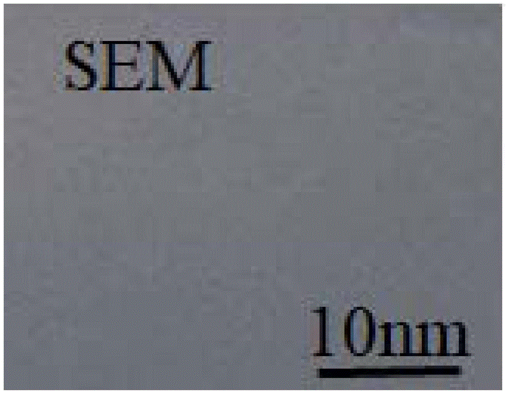
图3是发明实施例6中对AlGaN材料进行刻蚀后的SEM图。FIG. 3 is an SEM image of AlGaN material after etching in Embodiment 6 of the invention.
具体实施方式Detailed ways
鉴于现有技术中的不足,本案发明人经长期研究和大量实践,得以提出本发明的技术方案。如下将对该技术方案、其实施过程及原理等作进一步的解释说明。In view of the deficiencies in the prior art, the inventor of this case was able to propose the technical solution of the present invention after long-term research and extensive practice. The technical solution, its implementation process and principle will be further explained as follows.
本发明实施例提供了一种AlGaN材料的刻蚀方法,包括:将包含HBr、O2和SF6的刻蚀气体转化为等离子体,并使所述等离子体与AlGaN材料接触。An embodiment of the present invention provides an etching method for an AlGaN material, comprising: converting an etching gas containing HBr, O 2 and SF 6 into plasma, and making the plasma contact the AlGaN material.
在一些较为具体的实施方案中,预先将O2和SF6混合形成混合气体,再以所述混合气体与HBr气体作为刻蚀气体。In some more specific embodiments, O 2 and SF 6 are mixed in advance to form a mixed gas, and then the mixed gas and HBr gas are used as the etching gas.
在一些较为具体的实施方案中,所述混合气体中O2和SF6的摩尔比为(1.5-2):1,所述HBr气体与由O2和SF6形成的混合气体的摩尔比为(6-25):(1-4)。In some more specific embodiments, the molar ratio of O2 and SF6 in the mixed gas is (1.5-2): 1, and the molar ratio of the HBr gas to the mixed gas formed by O2 and SF6 is (6-25): (1-4).
在一些较为具体的实施方案中,所述的AlGaN材料的刻蚀方法包括:采用功率为500-800W的等离子体功率源将所述刻蚀气体转化为等离子体。In some more specific embodiments, the AlGaN material etching method includes: using a plasma power source with a power of 500-800W to convert the etching gas into plasma.
本发明实施例提供了一种AlGaN材料的刻蚀方法,包括:An embodiment of the present invention provides an etching method for an AlGaN material, including:
将AlGaN材料置于刻蚀设备的刻蚀腔室内;placing the AlGaN material in an etching chamber of an etching device;
向所述刻蚀腔室内通入包含HBr、O2和SF6的刻蚀气体,且以等离子体功率源将所述刻蚀气体转化为等离子体,再使所述等离子体与AlGaN材料表面的选定区域接触。Into the etching chamber, the etching gas containing HBr, O 2 and SF 6 is introduced, and the etching gas is converted into plasma with a plasma power source, and then the plasma is combined with the surface of the AlGaN material Selected area contacts.
在一些较为具体的实施方案中,所述的AlGaN材料的刻蚀方法具体包括:先将O2和SF6混合形成混合气体,再将由所述O2和SF6形成的混合气体和HBr气体通入所述刻蚀腔室。In some more specific embodiments, the AlGaN material etching method specifically includes: first mixing O 2 and SF 6 to form a mixed gas, and then passing the mixed gas formed by the O 2 and SF 6 and HBr gas into the etching chamber.
在一些较为具体的实施方案中,所述的AlGaN材料的刻蚀方法具体包括:In some more specific embodiments, the etching method of the AlGaN material specifically includes:
向所述刻蚀腔室内通入所述的刻蚀气体,控制其中HBr气体的流量为80-200sccm、由O2与SF6形成的混合气体的流量为10-40sccm、载气流量为80-400sccm,Introduce the etching gas into the etching chamber, control the flow rate of HBr gas to 80-200 sccm, the flow rate of the mixed gas formed by O2 and SF6 to be 10-40 sccm, and the flow rate of the carrier gas to be 80-200 sccm. 400 sccm,
以及,控制所述刻蚀腔室内的压力为20-80mtorr,以功率为500-800W的等离子体功率源将所述刻蚀气体转化为等离子体,且在所述AlGaN材料上施加200-300V的偏置电压,并使所述等离子体与AlGaN材料表面的选定区域接触。And, control the pressure in the etching chamber to be 20-80mtorr, convert the etching gas into plasma with a plasma power source with a power of 500-800W, and apply 200-300V to the AlGaN material bias voltage and bring the plasma into contact with selected regions of the surface of the AlGaN material.
在一些较为具体的实施方案中,所述混合气体中,O2和SF6的摩尔比为(1.5-2):1,所述HBr气体与由O2和SF6形成的混合气体的摩尔比为(6-25):(1-4)。In some more specific embodiments, in the mixed gas, the molar ratio of O2 and SF6 is (1.5-2):1, and the molar ratio of the HBr gas to the mixed gas formed by O2 and SF6 For (6-25): (1-4).
在一些较为具体的实施方案中,所述的AlGaN材料的刻蚀方法还包括:将AlGaN材料置于刻蚀设备的刻蚀腔室内,并将所述刻蚀腔室内的温度升高至500-600℃,然后使用氮气吹扫AlGaN材料表面,完成对AlGaN材料的表面清洁处理,而后再对所述AlGaN材料进行刻蚀。In some more specific embodiments, the etching method of the AlGaN material also includes: placing the AlGaN material in the etching chamber of the etching equipment, and raising the temperature in the etching chamber to 500- 600° C., and then use nitrogen to blow the surface of the AlGaN material to complete the surface cleaning treatment of the AlGaN material, and then etch the AlGaN material.
本发明实施例提供了一种AlGaN器件的制作方法,包括以所述的AlGaN材料的刻蚀方法对所述AlGaN器件中的AlGaN层进行干法刻蚀的步骤;当然,所述的AlGaN器件的制作方法还包括在对AlGaN层进行刻蚀前后制作其他结构的步骤,其中制作其他结构的步骤根据具体器件类型不同而定,在此不做具体的限定。An embodiment of the present invention provides a method for manufacturing an AlGaN device, including the step of performing dry etching on the AlGaN layer in the AlGaN device using the AlGaN material etching method; of course, the AlGaN device The fabrication method also includes the steps of fabricating other structures before and after etching the AlGaN layer, wherein the steps of fabricating other structures depend on different types of specific devices, and are not specifically limited here.
如下将结合附图对该技术方案、其实施过程及原理等作进一步的解释说明,除非特别说明的之外,本发明实施例中AlGaN层、应力缓冲层等结构层的制作工艺均为本领域技术人员已知的,或者,可以直接采用市购的AlGaN外延片,在此不做具体的限定,应理解,本发明实施例主要是对本发明提供的AlGaN材料的刻蚀方法进行解释和说明,其中所采用的刻蚀设备、生长设备等均是本领域技术人员已知的,在此不做具体的限定。The technical solution, its implementation process and principle will be further explained in conjunction with the accompanying drawings as follows. Unless otherwise specified, the manufacturing processes of the AlGaN layer, the stress buffer layer and other structural layers in the embodiments of the present invention are all in the field. Known by the skilled person, alternatively, a commercially available AlGaN epitaxial wafer can be directly used, and no specific limitation is made here. It should be understood that the embodiment of the present invention mainly explains and illustrates the etching method of the AlGaN material provided by the present invention. The etching equipment and growth equipment used therein are all known to those skilled in the art, and are not specifically limited here.
请参阅图2,一种AlGaN材料的刻蚀方法,具体包括如下步骤:Please refer to FIG. 2, an etching method for an AlGaN material, which specifically includes the following steps:
1)提供衬底,在衬底上形成AlGaN层;1) Provide a substrate and form an AlGaN layer on the substrate;
需要说明的是,所述衬底可以为蓝宝石衬底、碳化硅衬底或者氮化镓衬底;为了提高AlGaN层的晶体质量,在选用蓝宝石或者碳化硅作为衬底时,可以先在衬底上形成应力缓冲层,再在所述应力缓冲层上形成AlGaN层,所述应力缓冲层的材质可以为氮化铝,而在选用氮化镓作为衬底时,由于AlGaN层与氮化镓衬底的晶格匹配较好,因此不用考虑晶格失配的问题,则无需在氮化镓衬底上形成应力缓冲层;It should be noted that the substrate can be a sapphire substrate, a silicon carbide substrate or a gallium nitride substrate; in order to improve the crystal quality of the AlGaN layer, when selecting sapphire or silicon carbide as the substrate, the substrate can be A stress buffer layer is formed on the stress buffer layer, and then an AlGaN layer is formed on the stress buffer layer. The material of the stress buffer layer can be aluminum nitride, and when gallium nitride is selected as the substrate, since the AlGaN layer and the gallium nitride substrate The lattice matching of the bottom is better, so there is no need to consider the problem of lattice mismatch, and there is no need to form a stress buffer layer on the gallium nitride substrate;
应理解的,根据所要制作的器件类型不同、AlGaN层的作为不同器件的功能层的位置和厚度的不同,所述AlGaN层的Al含量也不同,形成AlGaN层的厚度也不同,本发明主要研究针对AlGaN的刻蚀工艺,因此,对AlGaN层的Al的含量以及其厚度并不做具体的限定;It should be understood that, depending on the type of device to be fabricated, the position and thickness of the functional layer of the AlGaN layer as a different device, the Al content of the AlGaN layer is also different, and the thickness of the AlGaN layer formed is also different. The present invention mainly studies For the etching process of AlGaN, therefore, there is no specific limitation on the Al content and thickness of the AlGaN layer;
另外,由于沉积形成AlGaN层的过程通常在MOCVD设备中进行,而刻蚀时是在ICP设备中进行,因此,在沉积形成AlGaN层之后,需要将待刻蚀的AlGaN材料取出,然后运送至ICP设备中,在运输过程中虽然对运输环境有要求,但不可避免的AlGaN层会接触外界环境,因此在将AlGaN材料运送至ICP设备中时,需要先对AlGaN层进行清洗处理,清洗处理的过程包括:先将刻蚀腔室内的温度加热到500-600℃,然后使用氮气吹扫AlGaN层的表面,500-600℃的温度环境能够去除AlGaN层表面可能吸附的水汽,氮气吹扫能够将AlGaN层表面可能粘附的杂质物质去掉,防止AlGaN层表面粘附的杂质难以在刻蚀中去除;In addition, since the deposition and formation of the AlGaN layer is usually carried out in MOCVD equipment, and the etching is carried out in the ICP equipment, therefore, after the AlGaN layer is deposited and formed, the AlGaN material to be etched needs to be taken out and then transported to the ICP In the equipment, although there are requirements for the transportation environment during the transportation process, the AlGaN layer will inevitably come into contact with the external environment. Therefore, when the AlGaN material is transported to the ICP equipment, the AlGaN layer needs to be cleaned first. The cleaning process Including: first heating the temperature in the etching chamber to 500-600°C, and then using nitrogen to purge the surface of the AlGaN layer. The temperature environment of 500-600°C can remove the water vapor that may be adsorbed on the surface of the AlGaN layer. Remove the impurity substances that may adhere to the surface of the AlGaN layer to prevent the impurities adhered to the surface of the AlGaN layer from being difficult to remove during etching;
当然,根据需要制作的器件类型和刻蚀目标的不同,可以对AlGaN层进行不同厚度和不同尺寸的刻蚀,本发明主要解释的是对AlGaN层表面的刻蚀,对目标区域的大小和刻蚀深度先不做要求,后续可以根据本发明的刻蚀方法对AlGaN层进行针对区域性的刻蚀;Of course, depending on the type of device to be manufactured and the etching target, the AlGaN layer can be etched with different thicknesses and sizes. The etching depth is not required at first, and the AlGaN layer can be etched regionally according to the etching method of the present invention;
2)在对AlGaN层表面进行表面清洁处理之后或不进行表面清洁处理,使用电感耦合等离子体刻蚀(ICP)设备对AlGaN层进行刻蚀,具体包括:2) After performing surface cleaning treatment on the surface of the AlGaN layer or without surface cleaning treatment, use inductively coupled plasma etching (ICP) equipment to etch the AlGaN layer, specifically including:
将AlGaN材料置于电感耦合等离子体刻蚀(ICP)刻蚀设备的刻蚀腔室中,并向所述刻蚀腔室中通入HBr气体以及由O2和SF6混合形成的混合气体共同作为刻蚀气体,控制其中的HBr的流量为80-200sccm,载气的流量为80-400sccm,由O2和SF6形成的混合气体的流量为10-40sccm,其中, HBr为主刻蚀气体, O2和SF6作为辅助刻蚀气体,载气为惰性气体,例如He气或者Ar气等,The AlGaN material is placed in the etching chamber of the inductively coupled plasma etching (ICP) etching equipment, and the HBr gas and the mixed gas formed by mixing O2 and SF6 are introduced into the etching chamber together. As etching gas, control the flow rate of HBr wherein to be 80-200sccm, the flow rate of carrier gas to be 80-400sccm, the flow rate of the mixed gas formed by O2 and SF6 to be 10-40sccm, wherein, HBr is the main etching gas , O 2 and SF 6 are used as auxiliary etching gases, and the carrier gas is an inert gas, such as He gas or Ar gas, etc.,
以及,控制所述刻蚀腔室内的压力为20-80mtorr,以功率为500-800W的等离子体功率源将所述刻蚀气体转化为等离子体,且在所述AlGaN材料上施加200-300V的偏置电压,并使所述等离子体与AlGaN材料表面的选定区域接触,从而实现对AlGaN材料的刻蚀。And, control the pressure in the etching chamber to be 20-80mtorr, convert the etching gas into plasma with a plasma power source with a power of 500-800W, and apply 200-300V to the AlGaN material The bias voltage is applied, and the plasma is brought into contact with a selected area on the surface of the AlGaN material, thereby realizing etching of the AlGaN material.
需要说明的是,在通入刻蚀腔室之前,先将O2和SF6按照摩尔比(1.5-2):1进行混合形成混合气体,之后再将O2和SF6的混合气体按照流量为10-40sccm通入刻蚀腔室,且所述HBr气体与由O2和SF6形成的混合气体的摩尔比为(6-25):(1-4)。It should be noted that before entering the etching chamber, O 2 and SF 6 are mixed according to the molar ratio (1.5-2): 1 to form a mixed gas, and then the mixed gas of O 2 and SF 6 is mixed according to the flow rate 10-40 sccm is passed into the etching chamber, and the molar ratio of the HBr gas to the mixed gas formed by O 2 and SF 6 is (6-25):(1-4).
本发明实施例提供的一种AlGaN材料的刻蚀方法,在刻蚀过程中,以HBr作为主刻蚀气体,由于Br自由基的化学活性远低于卤族其他元素的自由基的化学活性,卤族元素的电负性为:F(3.98)>Cl(3.16)>Br(2.96),Br离子的电负性较低,在对AlGaN材料的刻蚀过程不会与AlGaN反应形成AlGaBr这种物质,且刻蚀比较温和,不会对AlGaN材料刻蚀区域或形成的刻蚀结构(例如凹槽等)的侧壁造成较大的刻蚀损伤,且刻蚀后的刻蚀区域表面较为平坦,同时,本发明实施例以O2和SF6作为辅助刻蚀气体,且通入量较少;由于O2具有较强的氧化性能,O2的存在可以防止刻蚀过程中残余物的形成和堆积,以及,还能够对刻蚀过程中产生的损伤区域进行氧化,并借助HBr气体将氧化的区域刻蚀去除,有助于形成平整的形貌;而SF6的刻蚀速率较快,从而能够提高刻蚀速率,但如果单独的使用SF6进行刻蚀,虽然由于F的电负性最高,刻蚀速率会比较快,但刻蚀过程中会对刻蚀结构(例如刻蚀凹槽)的底部和侧壁造成损伤,不利于形成平坦的沟槽形貌;因此,在辅助刻蚀气体中,O2的摩尔量要多于SF6的摩尔量,这样可以在加快刻蚀的同时使用O2对刻蚀区域的侧壁进行氧化修复,从而有利于加快刻蚀速度,并形成表面平整的形貌,因此,在本发明中O2和SF6的摩尔比控制在(1.5-2):1。In an etching method for an AlGaN material provided in an embodiment of the present invention, HBr is used as the main etching gas during the etching process. Since the chemical activity of Br radicals is much lower than that of other halogen elements, The electronegativity of halogen elements is: F (3.98) > Cl (3.16) > Br (2.96), the electronegativity of Br ions is low, and it will not react with AlGaN to form AlGaBr during the etching process of AlGaN materials. Substance, and the etching is relatively mild, it will not cause large etching damage to the sidewall of the etched area of AlGaN material or the formed etched structure (such as grooves, etc.), and the surface of the etched area after etching is relatively flat , at the same time, the embodiment of the present invention uses O 2 and SF 6 as auxiliary etching gases, and the amount of feed is small; because O 2 has a strong oxidation performance, the presence of O 2 can prevent the formation of residues in the etching process and accumulation, as well as, it can also oxidize the damaged area generated during the etching process, and remove the oxidized area by etching with the help of HBr gas, which helps to form a flat shape; while the etching rate of SF 6 is faster, Thereby, the etching rate can be increased, but if SF6 is used for etching alone, although the etching rate will be faster due to the highest electronegativity of F, the etching process (such as etching grooves) will be relatively fast. ) causes damage to the bottom and sidewalls, which is not conducive to the formation of flat trench morphology; therefore, in the auxiliary etching gas, the molar amount of O 2 is more than that of SF 6 , which can speed up the etching at the same time Oxygen is used to repair the sidewall of the etching region, which helps to accelerate the etching rate and form a smooth surface. Therefore, in the present invention, the molar ratio of O and SF is controlled at (1.5-2 ):1.
如下将结合具体实施例对该技术方案、其实施过程及原理等作进一步的解释说明。The technical solution, its implementation process and principle will be further explained in conjunction with specific embodiments as follows.
在如下实施例中,通过选用不同的刻蚀气体对相同的AlGaN材料进行干法刻蚀,并观测各实施例刻蚀区域的刻蚀的深度以及刻蚀形貌。In the following embodiments, the same AlGaN material is dry-etched by selecting different etching gases, and the etching depth and etching morphology of the etching area of each embodiment are observed.
如下实施例中所采用的载气均采用Ar气,并保持载气的流量一致,即80-400sccm,且控制如下实施例中的刻蚀时间相同,需要说明的是,如下实施例中所采用的电感耦合等离子体刻蚀(ICP)刻蚀设备的型号、规格均是相同的,其中,相同的AlGaN材料是指AlGaN材料的制作工艺、尺寸规格等均相同。The carrier gas used in the following examples is Ar gas, and the flow rate of the carrier gas is kept consistent, that is, 80-400 sccm, and the etching time in the following examples is controlled to be the same. It should be noted that the following examples use The models and specifications of the inductively coupled plasma etching (ICP) etching equipment are the same, and the same AlGaN material refers to the same manufacturing process and size specifications of the AlGaN material.
实施例1Example 1
一种AlGaN材料的刻蚀方法,包括如下步骤:A kind of etching method of AlGaN material, comprises the steps:
将AlGaN材料置于电感耦合等离子体刻蚀(ICP)刻蚀设备的刻蚀腔室中,向所述刻蚀腔室内通入HBr作为刻蚀气体,且控制所述HBr的流量为150sccm,以及,控制所述刻蚀腔室内的压力为60 mtorr,以功率为550W的等离子体功率源将所述刻蚀气体转化为等离子体,且在所述AlGaN材料上施加250V的偏置电压,并使所述等离子体与AlGaN材料表面的选定区域接触,从而实现对AlGaN材料选定区域的刻蚀,刻蚀时间30S,刻蚀后的AlGaN材料记为样品1;本实施例中刻蚀参数以及刻蚀后的AlGaN材料表面粗糙度如表1所示。placing the AlGaN material in an etching chamber of an inductively coupled plasma etching (ICP) etching device, feeding HBr into the etching chamber as an etching gas, and controlling the flow rate of the HBr to 150 sccm, and , controlling the pressure in the etching chamber to be 60 mtorr, converting the etching gas into plasma with a plasma power source with a power of 550W, and applying a bias voltage of 250V on the AlGaN material, and making The plasma is in contact with a selected area on the surface of the AlGaN material, thereby realizing the etching of the selected area of the AlGaN material, the etching time is 30 seconds, and the etched AlGaN material is recorded as sample 1; in this embodiment, the etching parameters and Table 1 shows the surface roughness of the etched AlGaN material.
实施例2Example 2
一种AlGaN材料的刻蚀方法,包括如下步骤:A kind of etching method of AlGaN material, comprises the steps:
将AlGaN材料置于电感耦合等离子体刻蚀(ICP)刻蚀设备的刻蚀腔室中,向所述刻蚀腔室内通入SF6作为刻蚀气体,且控制所述SF6的流量为150sccm,以及,控制所述刻蚀腔室内的压力为60 mtorr,以功率为550W的等离子体功率源将所述刻蚀气体转化为等离子体,且在所述AlGaN材料上施加250V的偏置电压,并使所述等离子体与AlGaN材料表面的选定区域接触,从而实现对AlGaN材料选定区域的刻蚀,刻蚀时间30S,刻蚀后的AlGaN材料记为样品2;本实施例中刻蚀参数以及刻蚀后的AlGaN材料表面粗糙度如表1所示。The AlGaN material is placed in the etching chamber of the inductively coupled plasma etching (ICP) etching equipment, and SF 6 is introduced into the etching chamber as an etching gas, and the flow rate of the SF 6 is controlled to be 150 sccm , and, controlling the pressure in the etching chamber to be 60 mtorr, converting the etching gas into plasma with a plasma power source with a power of 550W, and applying a bias voltage of 250V on the AlGaN material, And make the plasma contact with the selected area on the surface of the AlGaN material, so as to realize the etching of the selected area of the AlGaN material, the etching time is 30S, and the AlGaN material after etching is recorded as sample 2; in this embodiment, the etching The parameters and the surface roughness of the AlGaN material after etching are shown in Table 1.
实施例3Example 3
一种AlGaN材料的刻蚀方法,包括如下步骤:A kind of etching method of AlGaN material, comprises the steps:
将AlGaN材料置于电感耦合等离子体刻蚀(ICP)刻蚀设备的刻蚀腔室中,向所述刻蚀腔室内通入HBr和SF6作为刻蚀气体,其中,所述HBr为主刻蚀气体,SF6为辅助刻蚀气体,且控制所述HBr的流量为150sccm,SF6的流量为25sccm,以及,控制所述刻蚀腔室内的压力为60 mtorr,以功率为550W的等离子体功率源将所述刻蚀气体转化为等离子体,且在所述AlGaN材料上施加250V的偏置电压,并使所述等离子体与AlGaN材料表面的选定区域接触,从而实现对AlGaN材料选定区域的刻蚀,刻蚀时间30S,刻蚀后的AlGaN材料记为样品3;本实施例中刻蚀参数以及刻蚀后的AlGaN材料表面粗糙度如表1所示。The AlGaN material is placed in an etching chamber of an inductively coupled plasma etching (ICP) etching device, and HBr and SF 6 are introduced into the etching chamber as etching gases, wherein the HBr is the main etching chamber Etching gas, SF 6 is an auxiliary etching gas, and the flow rate of controlling the HBr is 150 sccm, the flow rate of SF 6 is 25 sccm, and the pressure in the etching chamber is controlled to be 60 mtorr, with a power of 550W plasma The power source converts the etching gas into plasma, and applies a bias voltage of 250V on the AlGaN material, and makes the plasma contact with a selected area on the surface of the AlGaN material, thereby realizing the selection of the AlGaN material. For the etching of the region, the etching time is 30 seconds, and the etched AlGaN material is recorded as sample 3; the etching parameters and the surface roughness of the etched AlGaN material in this embodiment are shown in Table 1.
实施例4Example 4
一种AlGaN材料的刻蚀方法,包括如下步骤:A kind of etching method of AlGaN material, comprises the steps:
将AlGaN材料置于电感耦合等离子体刻蚀(ICP)刻蚀设备的刻蚀腔室中,向所述刻蚀腔室内通入HBr和O2作为刻蚀气体,其中,所述HBr为主刻蚀气体,O2为辅助刻蚀气体,且控制所述HBr的流量为150sccm,O2的流量为25sccm,以及,控制所述刻蚀腔室内的压力为60mtorr,以功率为550W的等离子体功率源将所述刻蚀气体转化为等离子体,且在所述AlGaN材料上施加250V的偏置电压,并使所述等离子体与AlGaN材料表面的选定区域接触,从而实现对AlGaN材料选定区域的刻蚀,刻蚀时间30S,刻蚀后的AlGaN材料记为样品4;本实施例中刻蚀参数以及刻蚀后的AlGaN材料表面粗糙度如表1所示。The AlGaN material is placed in an etching chamber of an inductively coupled plasma etching (ICP) etching equipment, and HBr and O2 are introduced into the etching chamber as etching gases, wherein the HBr is the main etching chamber Etching gas, O 2 is auxiliary etching gas, and the flow rate of controlling the HBr is 150 sccm, the flow rate of O 2 is 25 sccm, and the pressure in the etching chamber is controlled to be 60 mtorr, and the power is 550 W plasma power The source converts the etching gas into plasma, and applies a bias voltage of 250V on the AlGaN material, and makes the plasma contact with a selected area on the surface of the AlGaN material, thereby realizing the selected area of the AlGaN material The etching time is 30 seconds, and the etched AlGaN material is recorded as sample 4; the etching parameters and the surface roughness of the etched AlGaN material in this embodiment are shown in Table 1.
实施例5Example 5
一种AlGaN材料的刻蚀方法,包括如下步骤:A kind of etching method of AlGaN material, comprises the steps:
将AlGaN材料置于电感耦合等离子体刻蚀(ICP)刻蚀设备的刻蚀腔室中,向所述刻蚀腔室内通入SF6和O2作为刻蚀气体,其中,所述SF6为主刻蚀气体,O2为辅助刻蚀气体,且控制所述SF6的流量为150sccm,O2的流量为25sccm,以及,控制所述刻蚀腔室内的压力为60mtorr,以功率为550W的等离子体功率源将所述刻蚀气体转化为等离子体,且在所述AlGaN材料上施加250V的偏置电压,并使所述等离子体与AlGaN材料表面的选定区域接触,从而实现对AlGaN材料选定区域的刻蚀,刻蚀时间30S,刻蚀后的AlGaN材料记为样品5;本实施例中刻蚀参数以及刻蚀后的AlGaN材料表面粗糙度如表1所示。The AlGaN material is placed in an etching chamber of an inductively coupled plasma etching (ICP) etching device, and SF 6 and O 2 are introduced into the etching chamber as etching gases, wherein the SF 6 is The main etching gas, O 2 is the auxiliary etching gas, and the flow rate of the SF 6 is controlled to be 150 sccm, the flow rate of the O 2 is 25 sccm, and the pressure in the etching chamber is controlled to be 60 mtorr, and the power is 550W The plasma power source converts the etching gas into plasma, and applies a bias voltage of 250V on the AlGaN material, and makes the plasma contact with a selected area on the surface of the AlGaN material, thereby realizing the AlGaN material For the etching of the selected area, the etching time is 30 seconds, and the etched AlGaN material is recorded as sample 5; the etching parameters and the surface roughness of the etched AlGaN material in this embodiment are shown in Table 1.
实施例6Example 6
一种AlGaN材料的刻蚀方法,包括如下步骤:A kind of etching method of AlGaN material, comprises the steps:
将AlGaN材料置于电感耦合等离子体刻蚀(ICP)刻蚀设备的刻蚀腔室中,向所述刻蚀腔室内通入HBr、O2和SF6作为刻蚀气体,其中,所述HBr为主刻蚀气体,O2和SF6为辅助刻蚀气体,且控制其中的HBr的流量为150sccm, O2和SF6的混合气体的流量为25sccm,以及,控制所述刻蚀腔室内的压力为60 mtorr,以功率为550W的等离子体功率源将所述刻蚀气体转化为等离子体,且在所述AlGaN材料上施加250V的偏置电压,并使所述等离子体与AlGaN材料表面的选定区域接触,从而实现对AlGaN材料选定区域的刻蚀,刻蚀时间30S,刻蚀后的AlGaN材料记为样品6;本实施例中刻蚀参数以及刻蚀后的AlGaN材料表面粗糙度如表1以及图3所示,由图3可以看出,本实施例刻蚀后的AlGaN材料的表面平坦。The AlGaN material is placed in an etching chamber of an inductively coupled plasma etching (ICP) etching device, and HBr, O 2 and SF 6 are introduced into the etching chamber as etching gases, wherein the HBr Main etching gas, O 2 and SF 6 are auxiliary etching gases, and the flow rate of HBr in which is controlled is 150 sccm, and the flow rate of O 2 and SF 6 mixed gas is 25 sccm, and, controlling the flow rate in the etching chamber The pressure is 60 mtorr, the etching gas is converted into plasma with a plasma power source of 550W, and a bias voltage of 250V is applied to the AlGaN material, and the plasma and the surface of the AlGaN material are The selected area is contacted, so as to realize the etching of the selected area of the AlGaN material, the etching time is 30S, and the etched AlGaN material is recorded as sample 6; the etching parameters and the surface roughness of the etched AlGaN material in this embodiment As shown in Table 1 and FIG. 3 , it can be seen from FIG. 3 that the surface of the etched AlGaN material in this embodiment is flat.
需要说明的是,本实施例中的所述辅助刻蚀气体是先将O2和SF6按照摩尔比1.5:1混合形成混合气体,再将所述混合气体和HBr气体通入刻蚀腔体中共同作为刻蚀气体。It should be noted that the auxiliary etching gas in this embodiment is to first mix O2 and SF6 according to the molar ratio of 1.5:1 to form a mixed gas, and then pass the mixed gas and HBr gas into the etching chamber together as an etching gas.
实施例7Example 7
一种AlGaN材料的刻蚀方法,包括如下步骤:A kind of etching method of AlGaN material, comprises the steps:
将AlGaN材料置于电感耦合等离子体刻蚀(ICP)刻蚀设备的刻蚀腔室中,向所述刻蚀腔室内通入HBr、O2和SF6作为刻蚀气体,其中,所述HBr为主刻蚀气体,O2和SF6为辅助刻蚀气体,且控制其中的HBr的流量为150sccm, O2和SF6的混合气体的流量为25sccm,以及,控制所述刻蚀腔室内的压力为60 mtorr,以功率为550W的等离子体功率源将所述刻蚀气体转化为等离子体,且在所述AlGaN材料上施加250V的偏置电压,并使所述等离子体与AlGaN材料表面的选定区域接触,从而实现对AlGaN材料选定区域的刻蚀,刻蚀时间30S;刻蚀后的AlGaN材料记为样品7;本实施例中刻蚀参数以及刻蚀后的AlGaN材料表面粗糙度如表1所示。The AlGaN material is placed in an etching chamber of an inductively coupled plasma etching (ICP) etching device, and HBr, O 2 and SF 6 are introduced into the etching chamber as etching gases, wherein the HBr Main etching gas, O 2 and SF 6 are auxiliary etching gases, and the flow rate of HBr in which is controlled is 150 sccm, and the flow rate of O 2 and SF 6 mixed gas is 25 sccm, and, controlling the flow rate in the etching chamber The pressure is 60 mtorr, the etching gas is converted into plasma with a plasma power source of 550W, and a bias voltage of 250V is applied to the AlGaN material, and the plasma and the surface of the AlGaN material are The selected area is contacted, so as to realize the etching of the selected area of the AlGaN material, and the etching time is 30S; the etched AlGaN material is recorded as sample 7; the etching parameters and the surface roughness of the etched AlGaN material in this embodiment As shown in Table 1.
需要说明的是,本实施例中的所述辅助刻蚀气体是先将O2和SF6按照摩尔比1.8:1混合形成混合气体,再将所述混合气体和HBr气体通入刻蚀腔体中共同作为刻蚀气体。It should be noted that the auxiliary etching gas in this embodiment is to first mix O2 and SF6 according to the molar ratio of 1.8:1 to form a mixed gas, and then pass the mixed gas and HBr gas into the etching chamber together as an etching gas.
实施例8Example 8
一种AlGaN材料的刻蚀方法,包括如下步骤:A kind of etching method of AlGaN material, comprises the steps:
将AlGaN材料置于电感耦合等离子体刻蚀(ICP)刻蚀设备的刻蚀腔室中,向所述刻蚀腔室内通入HBr、O2和SF6作为刻蚀气体,其中,所述HBr为主刻蚀气体,O2和SF6为辅助刻蚀气体,且控制其中的HBr的流量为150sccm, O2和SF6的混合气体的流量为25sccm,以及,控制所述刻蚀腔室内的压力为60mtorr,以功率为550W的等离子体功率源将所述刻蚀气体转化为等离子体,且在所述AlGaN材料上施加250V的偏置电压,并使所述等离子体与AlGaN材料表面的选定区域接触,从而实现对AlGaN材料选定区域的刻蚀,刻蚀时间30S;刻蚀后的AlGaN材料记为样品8;本实施例中刻蚀参数以及刻蚀后的AlGaN材料表面粗糙度如表1所示。The AlGaN material is placed in an etching chamber of an inductively coupled plasma etching (ICP) etching device, and HBr, O 2 and SF 6 are introduced into the etching chamber as etching gases, wherein the HBr Main etching gas, O 2 and SF 6 are auxiliary etching gases, and the flow rate of HBr in which is controlled is 150 sccm, and the flow rate of O 2 and SF 6 mixed gas is 25 sccm, and, controlling the flow rate in the etching chamber The pressure is 60mtorr, the plasma power source with a power of 550W is used to convert the etching gas into plasma, and a bias voltage of 250V is applied to the AlGaN material, and the selective contact between the plasma and the surface of the AlGaN material In order to realize the etching of the selected area of the AlGaN material, the etching time is 30 seconds; the etched AlGaN material is recorded as sample 8; the etching parameters and the surface roughness of the etched AlGaN material in this embodiment are as follows: Table 1 shows.
需要说明的是,本实施例中的所述辅助刻蚀气体是先将O2和SF6按照摩尔比2:1混合形成混合气体,再将所述混合气体和HBr气体通入刻蚀腔体中共同作为刻蚀气体。It should be noted that the auxiliary etching gas in this embodiment is to first mix O2 and SF6 according to the molar ratio of 2:1 to form a mixed gas, and then pass the mixed gas and HBr gas into the etching chamber together as an etching gas.
实施例9Example 9
一种AlGaN材料的刻蚀方法,包括如下步骤:A kind of etching method of AlGaN material, comprises the steps:
将AlGaN材料置于电感耦合等离子体刻蚀(ICP)刻蚀设备的刻蚀腔室中,向所述刻蚀腔室内通入HBr、O2和SF6作为刻蚀气体,其中,所述HBr为主刻蚀气体,O2和SF6为辅助刻蚀气体,且控制其中的HBr的流量为220sccm, O2和SF6的混合气体的流量为25sccm,以及,控制所述刻蚀腔室内的压力为60 mtorr,以功率为550W的等离子体功率源将所述刻蚀气体转化为等离子体,且在所述AlGaN材料上施加250V的偏置电压,并使所述等离子体与AlGaN材料表面的选定区域接触,从而实现对AlGaN材料选定区域的刻蚀,刻蚀时间30S;刻蚀后的AlGaN材料记为样品9;本实施例中刻蚀参数以及刻蚀后的AlGaN材料表面粗糙度如表1所示。The AlGaN material is placed in an etching chamber of an inductively coupled plasma etching (ICP) etching device, and HBr, O 2 and SF 6 are introduced into the etching chamber as etching gases, wherein the HBr Main etching gas, O 2 and SF 6 are auxiliary etching gases, and the flow rate of HBr in which is controlled is 220 sccm, and the flow rate of O 2 and SF 6 mixed gas is 25 sccm, and, controlling the flow rate in the etching chamber The pressure is 60 mtorr, the etching gas is converted into plasma with a plasma power source of 550W, and a bias voltage of 250V is applied to the AlGaN material, and the plasma and the surface of the AlGaN material are The selected area is contacted, so as to realize the etching of the selected area of the AlGaN material, and the etching time is 30S; the etched AlGaN material is recorded as sample 9; the etching parameters and the surface roughness of the etched AlGaN material in this embodiment As shown in Table 1.
需要说明的是,本实施例中的所述辅助刻蚀气体是先将O2和SF6按照摩尔比1.8:1混合形成混合气体,再将所述混合气体和HBr气体通入刻蚀腔体中共同作为刻蚀气体。It should be noted that the auxiliary etching gas in this embodiment is to first mix O2 and SF6 according to the molar ratio of 1.8:1 to form a mixed gas, and then pass the mixed gas and HBr gas into the etching chamber together as an etching gas.
实施例10Example 10
一种AlGaN材料的刻蚀方法,包括如下步骤:A kind of etching method of AlGaN material, comprises the steps:
将AlGaN材料置于电感耦合等离子体刻蚀(ICP)刻蚀设备的刻蚀腔室中,向所述刻蚀腔室内通入HBr、O2和SF6作为刻蚀气体,其中,所述HBr为主刻蚀气体,O2和SF6为辅助刻蚀气体,且控制其中的HBr的流量为70sccm, O2和SF6的混合气体的流量为25sccm,以及,控制所述刻蚀腔室内的压力为60 mtorr,以功率为550W的等离子体功率源将所述刻蚀气体转化为等离子体,且在所述AlGaN材料上施加250V的偏置电压,并使所述等离子体与AlGaN材料表面的选定区域接触,从而实现对AlGaN材料选定区域的刻蚀;刻蚀后的AlGaN材料记为样品10;本实施例中刻蚀参数以及刻蚀后的AlGaN材料表面粗糙度如表1所示。The AlGaN material is placed in an etching chamber of an inductively coupled plasma etching (ICP) etching device, and HBr, O 2 and SF 6 are introduced into the etching chamber as etching gases, wherein the HBr The main etching gas, O 2 and SF 6 are auxiliary etching gases, and the flow rate of HBr in the control is 70 sccm, and the flow rate of O 2 and SF 6 mixed gas is 25 sccm, and, controlling the flow rate in the etching chamber The pressure is 60 mtorr, the etching gas is converted into plasma with a plasma power source of 550W, and a bias voltage of 250V is applied to the AlGaN material, and the plasma and the surface of the AlGaN material are The selected area is in contact, so as to realize the etching of the selected area of the AlGaN material; the etched AlGaN material is recorded as sample 10; the etching parameters and the surface roughness of the etched AlGaN material in this embodiment are shown in Table 1 .
需要说明的是,本实施例中的所述辅助刻蚀气体是先将O2和SF6按照摩尔比1.8:1混合形成混合气体,再将所述混合气体和HBr气体通入刻蚀腔体中共同作为刻蚀气体。It should be noted that the auxiliary etching gas in this embodiment is to first mix O2 and SF6 according to the molar ratio of 1.8:1 to form a mixed gas, and then pass the mixed gas and HBr gas into the etching chamber together as an etching gas.
实施例11Example 11
一种AlGaN材料的刻蚀方法,包括如下步骤:A kind of etching method of AlGaN material, comprises the steps:
将AlGaN材料置于电感耦合等离子体刻蚀(ICP)刻蚀设备的刻蚀腔室中,向所述刻蚀腔室内通入HBr、O2和SF6作为刻蚀气体,其中,所述HBr为主刻蚀气体,O2和SF6为辅助刻蚀气体,且控制其中的HBr的流量为150sccm, O2和SF6的混合气体的流量为25sccm,以及,控制所述刻蚀腔室内的压力为60 mtorr,以功率为550W的等离子体功率源将所述刻蚀气体转化为等离子体,且在所述AlGaN材料上施加250V的偏置电压,并使所述等离子体与AlGaN材料表面的选定区域接触,从而实现对AlGaN材料选定区域的刻蚀,刻蚀后的AlGaN材料记为样品11;本实施例中刻蚀参数以及刻蚀后的AlGaN材料表面粗糙度如表1所示。The AlGaN material is placed in an etching chamber of an inductively coupled plasma etching (ICP) etching device, and HBr, O 2 and SF 6 are introduced into the etching chamber as etching gases, wherein the HBr Main etching gas, O 2 and SF 6 are auxiliary etching gases, and the flow rate of HBr in which is controlled is 150 sccm, and the flow rate of O 2 and SF 6 mixed gas is 25 sccm, and, controlling the flow rate in the etching chamber The pressure is 60 mtorr, the etching gas is converted into plasma with a plasma power source of 550W, and a bias voltage of 250V is applied to the AlGaN material, and the plasma and the surface of the AlGaN material are The selected area is in contact, so as to realize the etching of the selected area of the AlGaN material, and the etched AlGaN material is recorded as sample 11; the etching parameters and the surface roughness of the etched AlGaN material in this embodiment are shown in Table 1 .
需要说明的是,本实施例中的所述辅助刻蚀气体是先将O2和SF6按照摩尔比1:2混合形成混合气体后再通入所述刻蚀腔室中。It should be noted that, the auxiliary etching gas in this embodiment is first mixed with O 2 and SF 6 at a molar ratio of 1:2 to form a mixed gas and then passed into the etching chamber.
实施例12Example 12
一种AlGaN材料的刻蚀方法,包括如下步骤:A kind of etching method of AlGaN material, comprises the steps:
将AlGaN材料置于电感耦合等离子体刻蚀(ICP)刻蚀设备的刻蚀腔室中,向所述刻蚀腔室内通入HBr、O2和SF6按照摩尔比20:1.8:1混合形成的混合气体作为刻蚀气体,且控制混合气体的流量为150sccm,以及,控制所述刻蚀腔室内的压力为60 mtorr,以功率为550W的等离子体功率源将所述刻蚀气体转化为等离子体,且在所述AlGaN材料上施加250V的偏置电压,并使所述等离子体与AlGaN材料表面的选定区域接触,从而实现对AlGaN材料选定区域的刻蚀,刻蚀时间为30S,刻蚀后的AlGaN材料记为样品12;本实施例中刻蚀参数以及刻蚀后的AlGaN材料表面粗糙度如表1所示。The AlGaN material is placed in the etching chamber of the inductively coupled plasma etching (ICP) etching equipment, and HBr, O 2 and SF 6 are mixed into the etching chamber according to the molar ratio of 20:1.8:1 to form The mixed gas is used as the etching gas, and the flow rate of the mixed gas is controlled to be 150 sccm, and the pressure in the etching chamber is controlled to be 60 mtorr, and the etching gas is converted into plasma by a plasma power source with a power of 550W body, and a bias voltage of 250V is applied to the AlGaN material, and the plasma is brought into contact with a selected area on the surface of the AlGaN material, so as to realize etching of the selected area of the AlGaN material, and the etching time is 30S, The etched AlGaN material is recorded as sample 12; the etching parameters and the surface roughness of the etched AlGaN material in this embodiment are shown in Table 1.
通过对实施例1-12获得的不同样品的SEM表面观测和对表面形貌粗糙度测量,为了便于对比,选定样品1的粗糙度的平均值为1,其余所有样品均与样品1的粗糙度进行对比,从粗糙度的比值可以直观反映出刻蚀后的形貌和粗糙度的关系。By the SEM surface observation of the different samples obtained in Examples 1-12 and the measurement of the surface roughness, for ease of comparison, the average value of the roughness of the selected sample 1 is 1, and all the other samples are the same as the roughness of the sample 1. The ratio of roughness can directly reflect the relationship between the etched morphology and roughness.
表1为实施例1-12中对AlGaN材料进行干法刻蚀的主要刻蚀参数以及刻蚀后的形貌表征Table 1 shows the main etching parameters for dry etching of AlGaN materials in Examples 1-12 and the morphology characterization after etching

从表1示出的对比实验结果可知,在相同的刻蚀时间内,对比样品1和样品2可以看出,以SF6作为刻蚀气体的刻蚀速度大于以HBr作为刻蚀气体的刻蚀速度,但以SF6进行刻蚀时会增加AlGaN材料刻蚀区域的表面粗糙度,且会对刻蚀区域的侧壁造成损伤,形成粗糙的表面;对比样品1和样品4、样品2和样品5可以看出,O2的加入能够在一定程度上减少AlGaN材料刻蚀区域的粗糙度,提高刻蚀区域的侧壁形貌的平整性;对比样品1和样品3可以看出,采用SF6能够提高刻蚀速度,但会使AlGaN材料刻蚀区域的表面粗糙程度加大。From the comparative experimental results shown in Table 1, it can be seen that in the same etching time, comparing sample 1 and sample 2, it can be seen that the etching rate using SF6 as the etching gas is greater than that of using HBr as the etching gas. speed, but etching with SF 6 will increase the surface roughness of the etched area of the AlGaN material, and will cause damage to the sidewall of the etched area, forming a rough surface; comparative sample 1 and sample 4, sample 2 and sample 5, it can be seen that the addition of O 2 can reduce the roughness of the etched area of the AlGaN material to a certain extent, and improve the smoothness of the sidewall morphology of the etched area; The etching speed can be increased, but the surface roughness of the etched area of the AlGaN material will be increased.
对比样品4和样品6可以看出,虽然在没有采用SF6的样品4的AlGaN材料刻蚀区域的粗糙度最小,表面最平滑,但其刻蚀速度较慢,在相同时间内,实施例6中的刻蚀速度(刻蚀深度)是实施例4的1.68倍。Comparing sample 4 and sample 6, it can be seen that although the roughness of the AlGaN material etching area of sample 4 without SF 6 is the smallest and the surface is the smoothest, its etching speed is slower. In the same time, embodiment 6 The etching rate (etching depth) in is 1.68 times that of Example 4.
与实施例6相比,实施例7提高了O2的用量,因此,样品7的刻蚀的深度有所提高,并且刻蚀的粗糙度减小,这是因为O2的加入能够提高氧化性能,提高了刻蚀速率,并且提高表面的平整性能;而对比实施例8,进一步提高O2的用量,并没有进一步提高刻蚀速率,这是因为过多的O2稀释了SF6,SF6与AlGaN材料的接触几率减小,进而降低了刻蚀速率。Compared with Example 6, Example 7 increases the amount of O2 , therefore, the etching depth of sample 7 is increased, and the etching roughness is reduced, because the addition of O2 can improve the oxidation performance , improved the etching rate, and improved the smoothness of the surface; and comparative example 8, further increasing the amount of O 2 , did not further increase the etching rate, because too much O 2 diluted SF 6 , SF 6 The probability of contact with AlGaN material is reduced, which in turn reduces the etch rate.
对比实施例9和实施例10,通过提高HBr的流量(样品9)和减少HBr的流量(样品10),以及,改变主刻蚀气体的流量,并不会单纯的增大或者减小刻蚀的速率,并且还会影响刻蚀表面的粗糙度,样品9的粗糙度明显提高,而实施例10中的样品10的粗糙度虽然较实施例7中的样品7的粗糙度减少,但刻蚀速率明显减少了很多。Comparing Example 9 and Example 10, by increasing the flow rate of HBr (sample 9) and reducing the flow rate of HBr (sample 10), and changing the flow rate of the main etching gas, it will not simply increase or decrease the etching rate, and also affects the roughness of the etched surface, the roughness of sample 9 is obviously improved, and although the roughness of sample 10 in embodiment 10 is less than the roughness of sample 7 in embodiment 7, the etching The speed is significantly reduced a lot.
将实施例6-8与实施例11相比,实施例11的刻蚀气体中的SF6含量更高,但实施例11并没有很显著的提高刻蚀的速率,但实施例11中的样品11的粗糙度却大大增加,这是因为SF6含量增大而O2含量减少时,由于表面的氧化性减少,SF6刻蚀会增大粗糙度,但由于O2氧化性减小,刻蚀速率并没有实质的提高很多。Comparing Examples 6-8 with Example 11, the SF content in the etching gas of Example 11 is higher, but Example 11 does not significantly improve the rate of etching, but the sample in Example 11 The roughness of 11 is greatly increased. This is because when the content of SF 6 increases and the content of O 2 decreases, the etching of SF 6 will increase the roughness due to the decrease of the oxidation of the surface, but the etching of SF 6 will increase the roughness due to the decrease of the oxidation of O 2 . The erosion rate did not increase substantially.
将实施例12与实施例6-11对比发现,将HBr、O2和SF6进行混合之后一起通入到刻蚀设备中作为刻蚀气体,并将所述刻蚀气体形成等离子体进行刻蚀,以与实施例7对比为例,实施例12中的刻蚀速率和刻蚀的粗糙度均有所减低,这是因为在将主刻蚀气体和辅助刻蚀气体预先混合好之后一起通入到ICP刻蚀装置中,由于SF6的相对分子量较HBr和O2要大很多,虽然在通入刻蚀腔室之前已将将气体进行了混合,但由于相对分子量大的SF6会向下沉,通入到刻蚀腔室中厚,SF6在混合气体的下方,而在被转化形成等离子体时,会较另外两种气体较延迟形成等离子体,这样就会使刻蚀速率有所减缓,不利于刻蚀速率的提升,而分别将SF6和O2的混合气体以及HBr通入时,由于SF6通入的管路与主刻蚀气体的管路不同,在刻蚀腔室内将气体形成等离子体时,各自管路的气体通入到刻蚀腔室中,能快速形成等离子体而不会出现SF6下沉的现象,因此并不会影响刻蚀速率。Comparing Example 12 with Examples 6-11, it is found that HBr, O 2 and SF 6 are mixed and then passed into the etching equipment together as an etching gas, and the etching gas is formed into a plasma for etching , taking the comparison with Example 7 as an example, both the etching rate and the etching roughness in Example 12 are reduced, because the main etching gas and the auxiliary etching gas are pre-mixed and fed together. In the ICP etching device, since the relative molecular weight of SF 6 is much larger than that of HBr and O 2 , although the gas has been mixed before being passed into the etching chamber, the SF 6 with a large relative molecular weight will go down Shen, thick in the etching chamber, SF 6 is under the mixed gas, and when it is converted to form plasma, it will delay the formation of plasma compared with the other two gases, which will make the etching rate somewhat slow down, which is not conducive to the improvement of the etching rate, and when the mixed gas of SF 6 and O 2 and HBr are introduced respectively, because the pipeline of SF 6 is different from the pipeline of the main etching gas, in the etching chamber When the gas is formed into a plasma, the gas in each pipeline is passed into the etching chamber, and the plasma can be formed rapidly without the sinking of SF 6 , so the etching rate will not be affected.
综上可得,在综合考虑刻蚀速率和刻蚀表面的平整度时,将O2和SF6按照摩尔比1.8:1混合形成混合气体后再通入所述刻蚀腔室中,刻蚀效果最好。In summary, when considering the etching rate and the flatness of the etching surface, O2 and SF6 are mixed according to the molar ratio of 1.8:1 to form a mixed gas and then passed into the etching chamber to etch best effect.
本发明实施例提供的一种AlGaN材料的刻蚀方法,采用不含氯元素的刻蚀气体刻蚀AlGaN,综合对比不同的刻蚀样品,使用HBr作为主刻蚀气体,以O2和SF6作为辅助刻蚀气体,能够兼顾刻蚀速度和刻蚀表面平整性,进而提高AlGaN材料的刻蚀速度和刻蚀质量。An etching method for an AlGaN material provided in an embodiment of the present invention uses an etching gas that does not contain chlorine to etch AlGaN, comprehensively compares different etching samples, uses HBr as the main etching gas, and uses O 2 and SF 6 As an auxiliary etching gas, it can balance the etching speed and etching surface smoothness, thereby improving the etching speed and etching quality of the AlGaN material.
需要说明的是,由于不同的物质(如硅或锗或砷体系的物质)使用的刻蚀腔室、刻蚀条件以及刻蚀过程中产生的副产物不同,本发明的实施例是针对AlGaN物质在ICP刻蚀时具有特定的副产物的缺陷进行改进提出的,与其他材料体系的刻蚀不同。It should be noted that due to the different etching chambers, etching conditions and by-products produced during the etching process for different substances (such as silicon or germanium or arsenic system substances), the embodiments of the present invention are aimed at AlGaN substances The improvement of defects with specific by-products during ICP etching is proposed differently from the etching of other material systems.
本发明实施例提供的一种AlGaN材料的刻蚀方法,通过以特定比例的O2和SF6作为辅助刻蚀气体与主刻蚀气体配合作用,不仅能够防止刻蚀残余物的形成及去除刻蚀残余物,形成平坦的刻蚀表面,也不会影响刻蚀的速率,并且,在刻蚀过程中,不使用含Cl的刻蚀气体,从而不会形成难以去除的AlGaClx凸起残余物,进而提高刻蚀的质量。An AlGaN material etching method provided in an embodiment of the present invention uses a specific ratio of O 2 and SF 6 as an auxiliary etching gas to cooperate with the main etching gas, which can not only prevent the formation of etching residues but also remove the etching residues. Etching residues, forming a flat etching surface, will not affect the etching rate, and, in the etching process, do not use Cl-containing etching gas, so that it will not form difficult-to-remove AlGaCl x raised residues , thereby improving the quality of etching.
应当理解,上述实施例仅为说明本发明的技术构思及特点,其目的在于让熟悉此项技术的人士能够了解本发明的内容并据以实施,并不能以此限制本发明的保护范围。凡根据本发明精神实质所作的等效变化或修饰,都应涵盖在本发明的保护范围之内。It should be understood that the above-mentioned embodiments are only to illustrate the technical concept and features of the present invention, the purpose of which is to enable those skilled in the art to understand the content of the present invention and implement it accordingly, and not to limit the protection scope of the present invention. All equivalent changes or modifications made according to the spirit of the present invention shall fall within the protection scope of the present invention.
Claims (8)
Priority Applications (1)
| Application Number | Priority Date | Filing Date | Title |
|---|---|---|---|
| CN202111576471.3A CN114242583B (en) | 2021-12-22 | 2021-12-22 | Etching method of AlGaN material and application thereof |
Applications Claiming Priority (1)
| Application Number | Priority Date | Filing Date | Title |
|---|---|---|---|
| CN202111576471.3A CN114242583B (en) | 2021-12-22 | 2021-12-22 | Etching method of AlGaN material and application thereof |
Publications (2)
| Publication Number | Publication Date |
|---|---|
| CN114242583A CN114242583A (en) | 2022-03-25 |
| CN114242583B true CN114242583B (en) | 2023-03-21 |
Family
ID=80760892
Family Applications (1)
| Application Number | Title | Priority Date | Filing Date |
|---|---|---|---|
| CN202111576471.3A Active CN114242583B (en) | 2021-12-22 | 2021-12-22 | Etching method of AlGaN material and application thereof |
Country Status (1)
| Country | Link |
|---|---|
| CN (1) | CN114242583B (en) |
Citations (3)
| Publication number | Priority date | Publication date | Assignee | Title |
|---|---|---|---|---|
| EP0539963A2 (en) * | 1991-10-29 | 1993-05-05 | Sony Corporation | Dry etching method of GaAs |
| JPH065558A (en) * | 1992-04-23 | 1994-01-14 | Sony Corp | Dry etching method |
| CN107591326A (en) * | 2017-08-29 | 2018-01-16 | 成都海威华芯科技有限公司 | A kind of groove etched method of low damage GaN/AlGaN HEMT gates |
Family Cites Families (20)
| Publication number | Priority date | Publication date | Assignee | Title |
|---|---|---|---|---|
| JPH06232092A (en) * | 1993-02-01 | 1994-08-19 | Sony Corp | Dry etching method |
| JP3298226B2 (en) * | 1993-04-22 | 2002-07-02 | ソニー株式会社 | Dry etching method |
| JP3478005B2 (en) * | 1996-06-10 | 2003-12-10 | ソニー株式会社 | Method for etching nitride-based compound semiconductor and method for manufacturing semiconductor device |
| JP4368963B2 (en) * | 1999-03-03 | 2009-11-18 | 株式会社日立製作所 | Etching method of compound semiconductor material |
| CN1272835C (en) * | 2003-09-19 | 2006-08-30 | 清华大学 | Dry etching method for gallium nitride materials |
| US20050139838A1 (en) * | 2003-12-26 | 2005-06-30 | Matsushita Electric Industrial Co., Ltd. | Semiconductor device and method for manufacturing semiconductor device |
| JP2005210105A (en) * | 2003-12-26 | 2005-08-04 | Matsushita Electric Ind Co Ltd | Semiconductor device and manufacturing method thereof |
| CN101162693B (en) * | 2006-10-09 | 2011-02-16 | 西安能讯微电子有限公司 | Gallium nitride surface low damnification etching |
| JP5714250B2 (en) * | 2010-07-14 | 2015-05-07 | 住友電工デバイス・イノベーション株式会社 | Manufacturing method of semiconductor device |
| JP2011142358A (en) * | 2011-04-22 | 2011-07-21 | Panasonic Corp | Nitride semiconductor device |
| JP6179937B2 (en) * | 2013-05-16 | 2017-08-16 | サムコ株式会社 | Plasma etching apparatus and plasma etching method |
| KR101605363B1 (en) * | 2014-11-06 | 2016-03-22 | 경북대학교 산학협력단 | Method for treating the surface of nitride semiconductor |
| JP6867221B2 (en) * | 2017-04-27 | 2021-04-28 | 大陽日酸株式会社 | Epitaxy growth device and epitaxial growth method |
| CN107293587B (en) * | 2017-07-24 | 2023-07-28 | 中国工程物理研究院电子工程研究所 | GaN/AlGaN gate groove low-damage etching method |
| RU2694164C1 (en) * | 2018-04-12 | 2019-07-09 | Федеральное государственное бюджетное учреждение науки Институт сверхвысокочастотной полупроводниковой электроники Российской академии наук | Method of dry etching of nitride layers |
| FR3091001B1 (en) * | 2018-12-21 | 2021-01-08 | Commissariat Energie Atomique | Method of etching a dielectric layer |
| CN110047748B (en) * | 2019-04-22 | 2022-03-04 | 江南大学 | Low-damage AlGaN/GaNHEMT gate groove etching method |
| FR3100923B1 (en) * | 2019-09-12 | 2021-10-01 | Commissariat Energie Atomique | Method of etching a layer based on a III-V material |
| CN113555283B (en) * | 2020-04-24 | 2024-04-05 | 江苏鲁汶仪器股份有限公司 | Method for etching heterojunction of GaN-based high-electron-mobility transistor |
| CN113823714B (en) * | 2021-11-24 | 2022-02-11 | 江苏第三代半导体研究院有限公司 | Manufacturing method of GaN-based Micro-LED structure and GaN-based Micro-LED array |
-
2021
- 2021-12-22 CN CN202111576471.3A patent/CN114242583B/en active Active
Patent Citations (3)
| Publication number | Priority date | Publication date | Assignee | Title |
|---|---|---|---|---|
| EP0539963A2 (en) * | 1991-10-29 | 1993-05-05 | Sony Corporation | Dry etching method of GaAs |
| JPH065558A (en) * | 1992-04-23 | 1994-01-14 | Sony Corp | Dry etching method |
| CN107591326A (en) * | 2017-08-29 | 2018-01-16 | 成都海威华芯科技有限公司 | A kind of groove etched method of low damage GaN/AlGaN HEMT gates |
Also Published As
| Publication number | Publication date |
|---|---|
| CN114242583A (en) | 2022-03-25 |
Similar Documents
| Publication | Publication Date | Title |
|---|---|---|
| US11087979B2 (en) | Cleaning method | |
| US10741393B2 (en) | Methods for bottom up fin structure formation | |
| CN101996876B (en) | Method for changing right-angled corners on tops of grooves with relatively large sizes into obvious round corners | |
| CN114242583B (en) | Etching method of AlGaN material and application thereof | |
| US20220319836A1 (en) | Nucleation layers for growth of gallium-and-nitrogen-containing regions | |
| CN216624314U (en) | Gallium nitride epitaxial structure | |
| CN114141919B (en) | Semiconductor substrate and preparation method thereof, semiconductor device and preparation method thereof | |
| KR102941509B1 (en) | Selective Silicon Deposition | |
| US20250029835A1 (en) | Integrated plasma clean and dielectric passivation deposition processes | |
| TW202111146A (en) | Method for manufacturing nitride semiconductor substrate | |
| CN114582707A (en) | Epitaxial wafer preparation method | |
| JP2006179917A (en) | Semiconductor wafer provided with semiconductor layer and electrical insulating layer thereunder, and manufacturing method thereof | |
| US10439047B2 (en) | Methods for etch mask and fin structure formation | |
| CN114121611B (en) | Gallium nitride epitaxial layer and method for forming the same | |
| JP2014216356A (en) | Semiconductor substrate, semiconductor substrate manufacturing method and composite substrate manufacturing method | |
| US9653282B2 (en) | Silicon-containing substrate cleaning procedure | |
| JP2014130914A (en) | Method for processing surface of semiconductor wafer, and method for producing processed semiconductor wafer | |
| CN118120066A (en) | Substrate processing for GaN growth | |
| CN118103951A (en) | Substrate processing for GaN growth | |
| CN118120043A (en) | Carbon Gap Filling Treatment |
Legal Events
| Date | Code | Title | Description |
|---|---|---|---|
| PB01 | Publication | ||
| PB01 | Publication | ||
| SE01 | Entry into force of request for substantive examination | ||
| SE01 | Entry into force of request for substantive examination | ||
| GR01 | Patent grant | ||
| GR01 | Patent grant |