CN114709233A - Method for integrating germanium p-i-n photodiode into image sensor structure - Google Patents
Method for integrating germanium p-i-n photodiode into image sensor structure Download PDFInfo
- Publication number
- CN114709233A CN114709233A CN202210504638.3A CN202210504638A CN114709233A CN 114709233 A CN114709233 A CN 114709233A CN 202210504638 A CN202210504638 A CN 202210504638A CN 114709233 A CN114709233 A CN 114709233A
- Authority
- CN
- China
- Prior art keywords
- germanium
- layer
- wafer
- silicon
- donor wafer
- Prior art date
- Legal status (The legal status is an assumption and is not a legal conclusion. Google has not performed a legal analysis and makes no representation as to the accuracy of the status listed.)
- Granted
Links
Images


Classifications
-
- H—ELECTRICITY
- H10—SEMICONDUCTOR DEVICES; ELECTRIC SOLID-STATE DEVICES NOT OTHERWISE PROVIDED FOR
- H10F—INORGANIC SEMICONDUCTOR DEVICES SENSITIVE TO INFRARED RADIATION, LIGHT, ELECTROMAGNETIC RADIATION OF SHORTER WAVELENGTH OR CORPUSCULAR RADIATION
- H10F39/00—Integrated devices, or assemblies of multiple devices, comprising at least one element covered by group H10F30/00, e.g. radiation detectors comprising photodiode arrays
- H10F39/011—Manufacture or treatment of image sensors covered by group H10F39/12
- H10F39/018—Manufacture or treatment of image sensors covered by group H10F39/12 of hybrid image sensors
-
- H—ELECTRICITY
- H10—SEMICONDUCTOR DEVICES; ELECTRIC SOLID-STATE DEVICES NOT OTHERWISE PROVIDED FOR
- H10F—INORGANIC SEMICONDUCTOR DEVICES SENSITIVE TO INFRARED RADIATION, LIGHT, ELECTROMAGNETIC RADIATION OF SHORTER WAVELENGTH OR CORPUSCULAR RADIATION
- H10F39/00—Integrated devices, or assemblies of multiple devices, comprising at least one element covered by group H10F30/00, e.g. radiation detectors comprising photodiode arrays
- H10F39/10—Integrated devices
- H10F39/12—Image sensors
- H10F39/18—Complementary metal-oxide-semiconductor [CMOS] image sensors; Photodiode array image sensors
- H10F39/184—Infrared image sensors
-
- H—ELECTRICITY
- H10—SEMICONDUCTOR DEVICES; ELECTRIC SOLID-STATE DEVICES NOT OTHERWISE PROVIDED FOR
- H10F—INORGANIC SEMICONDUCTOR DEVICES SENSITIVE TO INFRARED RADIATION, LIGHT, ELECTROMAGNETIC RADIATION OF SHORTER WAVELENGTH OR CORPUSCULAR RADIATION
- H10F39/00—Integrated devices, or assemblies of multiple devices, comprising at least one element covered by group H10F30/00, e.g. radiation detectors comprising photodiode arrays
- H10F39/10—Integrated devices
- H10F39/12—Image sensors
- H10F39/199—Back-illuminated image sensors
-
- Y—GENERAL TAGGING OF NEW TECHNOLOGICAL DEVELOPMENTS; GENERAL TAGGING OF CROSS-SECTIONAL TECHNOLOGIES SPANNING OVER SEVERAL SECTIONS OF THE IPC; TECHNICAL SUBJECTS COVERED BY FORMER USPC CROSS-REFERENCE ART COLLECTIONS [XRACs] AND DIGESTS
- Y02—TECHNOLOGIES OR APPLICATIONS FOR MITIGATION OR ADAPTATION AGAINST CLIMATE CHANGE
- Y02P—CLIMATE CHANGE MITIGATION TECHNOLOGIES IN THE PRODUCTION OR PROCESSING OF GOODS
- Y02P70/00—Climate change mitigation technologies in the production process for final industrial or consumer products
- Y02P70/50—Manufacturing or production processes characterised by the final manufactured product
Landscapes
- Solid State Image Pick-Up Elements (AREA)
Abstract
本发明提供一种将锗p‑i‑n光电二极管集成到图像传感器结构中的方法,其涉及半导体技术领域,其通过将氢离子(H+)注入锗供体晶圆至选定深度,以确定锗转移层的厚度;通过贝塔键合锗供体晶圆和硅目标晶圆的表面,将锗转移层与锗供体晶圆分离,得到锗硅混合晶圆;研磨锗硅混合晶圆的锗转移层的表面,将掺杂元素离子硼离子(B+)注入锗硅混合晶圆顶部的锗转移层,使锗转移层靠近表面的部分被注入硼而形成掺杂锗层;在锗光电二极管层中形成像素到像素之间的隔离结构,以界定光电二极管区域。本发明以低成本、相对更简单的制造工艺实现了高速、小像素尺寸、CMOS兼容的短波红外图像传感器(具有焦平面阵列),适于工业化大规模生产。

The present invention provides a method of integrating germanium p‑i‑n photodiodes into an image sensor structure, which relates to the field of semiconductor technology, by implanting hydrogen ions (H + ) into a germanium donor wafer to a selected depth to Determine the thickness of the germanium transfer layer; separate the germanium transfer layer from the germanium donor wafer by beta bonding the surfaces of the germanium donor wafer and the silicon target wafer to obtain a germanium-silicon hybrid wafer; grind the surface of the germanium-silicon hybrid wafer On the surface of the germanium transfer layer, doping element ions boron ions (B + ) are implanted into the germanium transfer layer on the top of the germanium-silicon mixed wafer, so that the part of the germanium transfer layer close to the surface is implanted with boron to form a doped germanium layer; in germanium photoelectric A pixel-to-pixel isolation structure is formed in the diode layer to define a photodiode region. The invention realizes a high-speed, small pixel size, CMOS-compatible short-wave infrared image sensor (having a focal plane array) with a low-cost and relatively simple manufacturing process, and is suitable for industrial mass production.
Description
技术领域technical field
本发明属于半导体技术领域,涉及一种将锗p-i-n光电二极管集成到图像传感器结构中的方法,具体涉及制造CMOS图像传感器的垂直p-i-n光电二极管。The invention belongs to the technical field of semiconductors, and relates to a method for integrating a germanium p-i-n photodiode into an image sensor structure, in particular to manufacturing a vertical p-i-n photodiode of a CMOS image sensor.
背景技术Background technique
目前,短波红外CMOS图像传感器(SWIR CMOS Image Sensor)已广泛应用于小型无人机系统、机动车辆系统、智能农业系统、监控系统等领域。如本领域所公知的,采用硅材料作为光电二极管对红外吸收的量子效率低下,特别是对于1μm以上的波段几乎没有吸收。与硅相比,基于锗的短波红外CMOS图像传感器可捕获来自可见光(0.4μm - 0.75μm)和更远波长(一直到1.6μm波长)的图像,而且性能与砷化铟镓(InGaAs)相当。基于砷化铟镓的CMOS图像传感器,尽管能够提供具有高量子效率及相对较低的暗电流的高质量焦平面阵列(FPA),但目前其制造工艺复杂、价格昂贵、产量低,难以大规模商业化应用。与砷化铟镓相反,锗在化学上与硅兼容,并且与硅CMOS制造工艺兼容。因此,用于短波红外CMOS图像传感器的锗基光电二极管的制造工艺更灵活、更具成本效益和可扩展性,并能打开消费者/大众市场的应用。At present, SWIR CMOS Image Sensor has been widely used in small unmanned aerial vehicle systems, motor vehicle systems, intelligent agricultural systems, monitoring systems and other fields. As is well known in the art, using silicon material as a photodiode has low quantum efficiency for infrared absorption, especially for the wavelength band above 1 μm, there is almost no absorption. Compared to silicon, germanium-based short-wave infrared CMOS image sensors can capture images from visible light (0.4μm - 0.75μm) and further wavelengths (up to 1.6μm wavelengths) with performance comparable to indium gallium arsenide (InGaAs). Although indium gallium arsenide-based CMOS image sensors can provide high-quality focal plane arrays (FPAs) with high quantum efficiency and relatively low dark current, their current manufacturing process is complex, expensive, and low-yield, making it difficult to large-scale commercial application. In contrast to indium gallium arsenide, germanium is chemically compatible with silicon and is compatible with silicon CMOS manufacturing processes. Therefore, the fabrication process of germanium-based photodiodes for SWIR CMOS image sensors is more flexible, cost-effective, and scalable, and opens up consumer/mass market applications.
在制造基于锗的CMOS图像传感器时,现有技术一般采用在硅目标晶圆上直接外延生长锗,但由于锗和硅之间4.2%的晶格失配,外延生长会产生失配位错和穿透位错(螺纹错位),因而缺陷较多、质量较低,影响探测信噪比和检测灵敏度。此问题目前尽管能够通过一些技术手段得到改善,但会增加器件结构和/或工艺复杂性,例如使用窄孔径选择性制造生长。此外,由于采用在硅目标晶圆上直接外延生长锗是在硅晶圆上低温生长锗,直接导致降低了锗层的质量。When fabricating germanium-based CMOS image sensors, the prior art generally employs direct epitaxial growth of germanium on a silicon target wafer, but due to the 4.2% lattice mismatch between germanium and silicon, the epitaxial growth will generate misfit dislocations and Threading dislocation (thread dislocation), so there are more defects and lower quality, which affects the detection signal-to-noise ratio and detection sensitivity. Although this problem can currently be ameliorated by some technical means, it will increase the complexity of the device structure and/or process, such as selective fabrication growth using narrow apertures. In addition, since the direct epitaxial growth of germanium on the silicon target wafer is used to grow germanium on the silicon wafer at a low temperature, the quality of the germanium layer is directly reduced.
基于工业市场及消费者/大众市场的应用需要,目前急需一种工艺更简单、成本更低且能够高效、稳定地将垂直锗p-i-n光电二极管集成到图像传感集成器件结构中的方法。Based on the application needs of the industrial market and the consumer/mass market, there is an urgent need for a method that is simpler in process, lower in cost, and can efficiently and stably integrate a vertical germanium p-i-n photodiode into an image sensing integrated device structure.
发明内容SUMMARY OF THE INVENTION
基于现有技术中存在的问题,本发明提供了一种将锗p-i-n光电二极管集成到图像传感器结构中的方法,具体涉及制造CMOS图像传感器的垂直p-i-n光电二极管,所述垂直p-i-n光电二极管优选为短波红外CMOS图像传感器的垂直p-i-n光电二极管。Based on the problems existing in the prior art, the present invention provides a method for integrating germanium p-i-n photodiodes into an image sensor structure, in particular to the fabrication of vertical p-i-n photodiodes for CMOS image sensors, the vertical p-i-n photodiodes are preferably short-wavelength Vertical p-i-n photodiodes for infrared CMOS image sensors.
依据本发明的技术方案,本发明提供了一种将锗p-i-n光电二极管集成到图像传感器结构中的方法,其包括以下步骤:According to the technical solution of the present invention, the present invention provides a method for integrating a germanium p-i-n photodiode into an image sensor structure, which includes the following steps:
步骤S1,提供锗供体晶圆;Step S1, providing a germanium donor wafer;
步骤S2,将氢离子(H+)注入锗供体晶圆至选定深度,以确定锗转移层的厚度,所述锗转移层为待转移的锗薄膜;Step S2, implanting hydrogen ions (H + ) into the germanium donor wafer to a selected depth to determine the thickness of the germanium transfer layer, where the germanium transfer layer is the germanium thin film to be transferred;
步骤S3,提供硅目标晶圆;Step S3, providing a silicon target wafer;
步骤S4,贝塔键合锗供体晶圆和硅目标晶圆的表面;Step S4, beta bonding the surfaces of the germanium donor wafer and the silicon target wafer;
步骤S5,将锗转移层与锗供体晶圆分离,得到锗硅混合晶圆;即使用热技术或机械技术,将键合粘附在硅目标晶圆上的锗转移层与锗供体晶圆分离,得到锗转移层和硅目标晶圆所构成的混合晶圆;In step S5, the germanium transfer layer and the germanium donor wafer are separated to obtain a germanium-silicon hybrid wafer; that is, thermal technology or mechanical technology is used to bond the germanium transfer layer and the germanium donor crystal on the silicon target wafer. The circle is separated to obtain a hybrid wafer composed of a germanium transfer layer and a silicon target wafer;
步骤S6,完成锗硅混合晶圆最终键合;Step S6, completing the final bonding of the germanium-silicon hybrid wafer;
步骤S7,研磨锗硅混合晶圆的锗转移层的表面;Step S7, grinding the surface of the germanium transfer layer of the germanium-silicon hybrid wafer;
步骤S8,将掺杂元素离子硼离子(B+)注入锗硅混合晶圆顶部的锗转移层,使锗转移层靠近表面的部分被注入硼而形成掺杂锗层,靠近硅目标晶圆的其余部分为未掺杂锗层;Step S8, implanting doped element ions boron ions (B + ) into the germanium transfer layer on the top of the germanium-silicon mixed wafer, so that the part of the germanium transfer layer close to the surface is implanted with boron to form a doped germanium layer, which is close to the silicon target wafer. The rest is the undoped germanium layer;
步骤S9,在锗光电二极管层中形成像素到像素之间的隔离结构,以界定光电二极管区域;Step S9, forming a pixel-to-pixel isolation structure in the germanium photodiode layer to define a photodiode region;
步骤S10,翻转锗硅混合晶圆;Step S10, flipping the silicon-germanium hybrid wafer;
步骤S11,提供一个涂布有临时黏合剂的载体。In step S11, a carrier coated with a temporary adhesive is provided.
其中,在步骤S11之后进一步包括以下步骤:Wherein, the following steps are further included after step S11:
步骤S12,通过临时黏合剂将锗硅混合晶圆的具有可流动的介质材料的一面临时键合/粘合到载体上;Step S12, temporarily bonding/adhering the side of the germanium-silicon hybrid wafer with the flowable dielectric material to the carrier through a temporary adhesive;
步骤S13,通过研磨去除大部分硅目标晶圆,直至像素隔离的底部13;Step S13, removing most of the silicon target wafer by grinding until the
步骤S14,在剩余硅层的朝外侧的表面沉积一层介电钝化层;Step S14, depositing a dielectric passivation layer on the outer surface of the remaining silicon layer;
步骤S15,对剩余硅层和掺杂锗层分别单独形成金属连接;Step S15, separately forming metal connections for the remaining silicon layer and the doped germanium layer;
步骤S16,在介电钝化层朝外侧的表面形成对齐标记。Step S16, forming alignment marks on the outer surface of the dielectric passivation layer.
其中,在步骤S16之后进一步包括以下步骤:Wherein, the following steps are further included after step S16:
步骤S17,提供硅控制和读出电路晶圆;Step S17, providing silicon control and readout circuit wafers;
步骤S18,将硅控制和读出电路晶圆的互联层朝外侧的表面与临时键合到载体的锗光电二极管层的介电钝化层朝外侧的表面相对接,通过二者上的对齐标记保证互联层和介电钝化层对齐,使锗光电二极管层的金属连接与互联层的电路相连接;Step S18, abutting the outer-facing surface of the interconnect layer of the silicon control and readout circuit wafer with the outer-facing surface of the dielectric passivation layer of the germanium photodiode layer temporarily bonded to the carrier, through alignment marks on the two Ensure that the interconnect layer and the dielectric passivation layer are aligned so that the metal connection of the germanium photodiode layer is connected to the circuit of the interconnect layer;
步骤S19,进行退火以完成键合;Step S19, annealing is performed to complete the bonding;
步骤S20,进行激光脱键/脱粘,移除载体;Step S20, carry out laser debonding/debonding, and remove the carrier;
步骤S21,通过化学机械研磨去除表面介电层;Step S21, removing the surface dielectric layer by chemical mechanical polishing;
步骤S22,在掺杂锗层及沟槽间介电层共同构成的表面沉积抗反射层;Step S22, depositing an anti-reflection layer on the surface formed by the doped germanium layer and the dielectric layer between the trenches;
步骤S23,在抗反射层顶部形成透镜层。Step S23, forming a lens layer on top of the anti-reflection layer.
优选地,在步骤S1中,对锗供体晶圆进行清洁和干燥,然后对锗供体晶圆表面进行研磨,所述研磨采用化学机械研磨工艺。Preferably, in step S1, the germanium donor wafer is cleaned and dried, and then the surface of the germanium donor wafer is ground by a chemical mechanical polishing process.
更优选地,步骤S1提供锗供体晶圆进一步包括,可在锗供体晶圆上沉积一层等离子增强化学气相沉积二氧化硅膜,二氧化硅膜厚度在10nm~90nm之间,以在随后步骤S2的氢离子注入期间保护锗供体晶圆的表面。More preferably, providing the germanium donor wafer in step S1 further includes, depositing a layer of plasma-enhanced chemical vapor deposition silicon dioxide film on the germanium donor wafer, and the silicon dioxide film thickness is between 10nm and 90nm, so that the The surface of the germanium donor wafer is protected during the subsequent hydrogen ion implantation in step S2.
进一步地,步骤S1提供锗供体晶圆进一步包括:在锗供体晶圆上沉积一层等离子增强化学气相沉积二氧化硅膜,二氧化硅膜厚度在10nm~90nm之间,以在随后步骤S2的氢离子注入期间保护锗供体晶圆的表面,并且该二氧化硅膜可在氢离子注入后移除。Further, the step S1 providing the germanium donor wafer further includes: depositing a layer of plasma enhanced chemical vapor deposition silicon dioxide film on the germanium donor wafer, the silicon dioxide film thickness is between 10nm and 90nm, so as to be used in subsequent steps The surface of the germanium donor wafer is protected during the hydrogen ion implantation of S2, and the silicon dioxide film can be removed after the hydrogen ion implantation.
更进一步地,步骤S2中的氢离子注入采用束线离子注入或等离子体浸没离子注入。Furthermore, the hydrogen ion implantation in step S2 adopts beamline ion implantation or plasma immersion ion implantation.
优选地,在所形成的锗转移层区域的顶面上沉积一层非晶态锗层。Preferably, an amorphous germanium layer is deposited on top of the formed germanium transfer layer region.
优选地,选择性剥离能量放置方法采用能量脉冲技术手段,所述能量脉冲就是通过提供局部能量脉冲。Preferably, the selective ablation energy placement method adopts energy pulse technology means, and the energy pulse is provided by providing local energy pulses.
更优选地,将氢离子(H+)注入锗供体晶圆,注入的氢离子捕获电子形成氢气,氢气在起泡层中形成微气泡层,平行于解理面,加热锗硅混合晶圆并沿解理面进行剥离。More preferably, hydrogen ions (H + ) are implanted into the germanium donor wafer, the implanted hydrogen ions capture electrons to form hydrogen gas, and the hydrogen gas forms a microbubble layer in the bubble layer, parallel to the cleavage plane, to heat the germanium-silicon hybrid wafer and peeled along the cleavage plane.
另外地,对于分离后的锗供体晶圆,通过研磨表面并对表面进行洁净处理后,可重复使用;即反复使用一片锗供体晶圆作为步骤S2的原料来产生锗转移层,直至其厚度薄至无法继续使用。In addition, the separated germanium donor wafer can be reused after grinding the surface and cleaning the surface; that is, a germanium donor wafer is repeatedly used as the raw material in step S2 to generate the germanium transfer layer until the The thickness is too thin to continue to use.
另外地,步骤S6完成锗硅混合晶圆最终键合中,最终键合步骤采用退火键合步骤,在小于或等于400摄氏度的工艺环境下持续数小时。In addition, in the final bonding of the germanium-silicon hybrid wafer in step S6, the final bonding step adopts an annealing bonding step, which lasts for several hours in a process environment of less than or equal to 400 degrees Celsius.
与现有技术相比,本发明的有益技术效果如下:Compared with the prior art, the beneficial technical effects of the present invention are as follows:
1、本发明以相对更简单的制造工艺,实现了高速、小像素尺寸的短波红外图像传感器的生产制造工艺。1. The present invention realizes the manufacturing process of the short-wave infrared image sensor with high speed and small pixel size with a relatively simpler manufacturing process.
2、本发明的技术方案实现了批量、高生产合格率生产制造的低成本、CMOS兼容的短波红外图像传感器(具有焦平面阵列)。2. The technical solution of the present invention realizes a low-cost, CMOS-compatible short-wave infrared image sensor (with a focal plane array) that can be produced in batches with high production yield.
3、采用本发明生产工艺制造的图像传感器,其具有从可见光到短波红外波长的更低的暗电流、更高的灵敏度。3. The image sensor manufactured by the production process of the present invention has lower dark current and higher sensitivity from visible light to short-wave infrared wavelengths.
4、本发明的技术方案利用针对离子注入、洁净、键合、退火、剥离、化学机械研磨等进行有机组合,使其生产工艺相对简单、技术成熟、适于工业化大规模生产。4. The technical solution of the present invention utilizes an organic combination of ion implantation, cleaning, bonding, annealing, peeling, chemical mechanical polishing, etc., so that the production process is relatively simple, the technology is mature, and it is suitable for industrialized large-scale production.
5、本发明将锗p-i-n光电二极管集成到图像传感器结构中的方法,采用锗-硅层转移技术获得高质量的光电二极管层单晶锗层,与在硅目标晶圆上直接外延生长锗层相比,具有更高的质量和更少的缺陷。5. The method of integrating germanium p-i-n photodiode into the image sensor structure of the present invention adopts the germanium-silicon layer transfer technology to obtain a high-quality single-crystal germanium layer of the photodiode layer, which is similar to the direct epitaxial growth of the germanium layer on the silicon target wafer. than, with higher quality and fewer defects.
6、采用本发明将锗p-i-n光电二极管集成到图像传感器结构中的方法制造的图像传感器,其为背面照明(BSI)传感器,采用堆叠式CMOS结构,即硅控制和读出电路位于像素层背面,这种结构提升或增加了在像素层捕获的入射光子数量,从而减少了噪声并提高了整体性能。6. The image sensor manufactured by the method of integrating the germanium p-i-n photodiode into the image sensor structure of the present invention is a backside illumination (BSI) sensor and adopts a stacked CMOS structure, that is, the silicon control and readout circuit is located on the back side of the pixel layer, This structure boosts or increases the number of incident photons captured at the pixel layer, reducing noise and improving overall performance.
7、本发明将锗p-i-n光电二极管集成到图像传感器结构中的方法的制造流程设计实现了垂直光电二极管的集成,垂直p-i-n光电二极管的金属触点均仅从背面接触到p型区和n型区,不会阻挡入射光子的照射,从而保证了捕获的入射光子数量。7. The manufacturing process design of the method for integrating the germanium p-i-n photodiode into the image sensor structure of the present invention realizes the integration of the vertical photodiode, and the metal contacts of the vertical p-i-n photodiode are only in contact with the p-type region and the n-type region from the back. , does not block the illumination of incident photons, thus ensuring the number of incident photons captured.
8、本发明将锗p-i-n光电二极管集成到图像传感器结构中的方法中,锗供体晶圆可重复利用以产生更多锗转移层,资源利用率更高,制造成本更低。8. In the method of integrating germanium p-i-n photodiodes into the image sensor structure of the present invention, the germanium donor wafer can be reused to generate more germanium transfer layers, the resource utilization rate is higher, and the manufacturing cost is lower.
附图说明Description of drawings
图1至图17为依据本发明将锗p-i-n光电二极管集成到图像传感器结构中的方法的制造流程示意图。1 to 17 are schematic diagrams illustrating the manufacturing flow of a method for integrating a germanium p-i-n photodiode into an image sensor structure according to the present invention.
图中附图标记所指示的部件名称如下:The names of the parts indicated by the reference numbers in the figures are as follows:
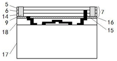
1、锗供体晶圆;2、锗转移层;3、硅目标晶圆;4、锗硅混合晶圆;5、掺杂锗层;6、未掺杂锗层;7、锗光电二极管层;8、隔离沟槽;9、沟槽间介电层;10、表面介电层;11、载体;12、临时黏合剂;13、像素隔离的底部;14、剩余硅层;15、金属连接;16、介电钝化层;17、硅控制和读出电路晶圆;18、互联层;19、抗反射层;20、滤光层;21、透镜层。1. germanium donor wafer; 2. germanium transfer layer; 3. silicon target wafer; 4. germanium-silicon hybrid wafer; 5. doped germanium layer; 6. undoped germanium layer; 7.
具体实施方式Detailed ways
下面将结合本发明实施例中的附图,对本发明实施例中的技术方案进行清楚、完整的描述。显然,所描述的实施例仅仅是本发明的一部分实施例,而不是全部的实施例。基于本发明中的实施例,本领域普通技术人员在没有做出创造性劳动前提下所获得的所有其他实施例,都属于本发明保护的范围。另外地,不应当将本发明的保护范围仅仅限制至下述具体结构或部件或具体参数。The technical solutions in the embodiments of the present invention will be clearly and completely described below with reference to the accompanying drawings in the embodiments of the present invention. Obviously, the described embodiments are only some, but not all, embodiments of the present invention. Based on the embodiments of the present invention, all other embodiments obtained by those of ordinary skill in the art without creative efforts shall fall within the protection scope of the present invention. Additionally, the scope of the present invention should not be limited only to the specific structures or components or specific parameters described below.
在本发明的描述中,需要理解的是,术语“上”、“下”、“前”、“后”、“左”、“右”、“顶”、“底”、“内”、“外”等指示的方位或位置关系为基于附图所示的方位或位置关系,仅是为了便于描述本发明和简化描述,而不是指示或暗示所指的装置或组件必须具有特定的方位、以特定的方位构造和操作,因此不能理解为对本发明的限制。In the description of the present invention, it should be understood that the terms "upper", "lower", "front", "rear", "left", "right", "top", "bottom", "inside", " The orientation or positional relationship indicated by "outside" is based on the orientation or positional relationship shown in the accompanying drawings, which is only for the convenience of describing the present invention and simplifying the description, rather than indicating or implying that the referred device or component must have a specific orientation, so as to The specific orientation configuration and operation are therefore not to be construed as limitations of the present invention.
本发明提供一种将锗p-i-n光电二极管集成到图像传感器结构中的方法,其通过将氢离子(H+)注入锗供体晶圆至选定深度,以确定锗转移层的厚度;通过贝塔键合锗供体晶圆和硅目标晶圆的表面,将锗转移层与锗供体晶圆分离,得到锗硅混合晶圆;研磨锗硅混合晶圆的锗转移层的表面,将掺杂元素离子硼离子(B+)注入锗硅混合晶圆顶部的锗转移层,使锗转移层靠近表面的部分被注入硼而形成掺杂锗层;在锗光电二极管层中形成像素到像素之间的隔离结构,以界定光电二极管区域。本发明以低成本、相对更简单的制造工艺实现了高速、小像素尺寸、CMOS兼容的短波红外图像传感器(具有焦平面阵列),适于工业化大规模生产。The present invention provides a method for integrating germanium pin photodiodes into image sensor structures by implanting hydrogen ions (H + ) into a germanium donor wafer to a selected depth to determine the thickness of the germanium transfer layer; via beta bonds Combine the surfaces of the germanium donor wafer and the silicon target wafer, and separate the germanium transfer layer from the germanium donor wafer to obtain a germanium-silicon mixed wafer; grind the surface of the germanium transfer layer of the germanium-silicon mixed wafer to remove doping elements Ion boron ions (B + ) are implanted into the germanium transfer layer on the top of the germanium-silicon hybrid wafer, so that the part of the germanium transfer layer close to the surface is implanted with boron to form a doped germanium layer; in the germanium photodiode layer, a pixel-to-pixel connection is formed. isolation structures to define photodiode regions. The invention realizes a high-speed, small pixel size, CMOS-compatible short-wave infrared image sensor (having a focal plane array) with a low-cost and relatively simple manufacturing process, and is suitable for industrial mass production.
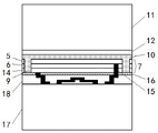
请参阅图17,采用本发明的方法制造的基于锗p-i-n光电二极管的图像传感器,从下至上依次包括硅控制和读出电路晶圆17、介电钝化层16、锗光电二极管层7、抗反射层19以及透镜层21。锗光电二极管层7为层叠结构,从下至上依次包括剩余硅层14、未掺杂锗层6和掺杂锗层5,其中未掺杂锗层6为本征层;剩余硅层14为n型区、掺杂锗层5为p型区;在另外的实施例中,剩余硅层14为p型区、掺杂锗层5为n型区。锗光电二极管层7中还包括贯穿其层叠结构设置的沟槽间介电层9,沟槽间介电层9将锗光电二极管层7划分为多个独立的像素区域。在每个像素区域中,介电钝化层16和锗光电二极管层7上自下而上设置有两个金属连接15,第一金属连接连接至剩余硅层14,第二金属连接连接至掺杂锗层5。硅控制和读出电路晶圆17的上部为具有电路的互联层18,互联层18的电路与金属连接15相连接。Referring to FIG. 17 , the image sensor based on germanium p-i-n photodiode manufactured by the method of the present invention includes silicon control and
优选地,在抗反射层19和透镜层21之间还具有滤光层20,滤光层可以选择性地传输特定波长范围的入射光,同时吸收剩余的光。Preferably, there is a
本发明的将锗p-i-n光电二极管集成到图像传感器结构中的方法,根据锗p-i-n光电二极管中p型区和n型区的上下顺序,可分为两种,可以理解的是,该两者的基本工艺原理是相同的。以将锗p-i-n光电二极管集成到图像传感器结构中的方法A(简称“方法A”)为例进行详细说明,请参阅图1至图17。The method for integrating a germanium p-i-n photodiode into an image sensor structure of the present invention can be divided into two types according to the upper and lower order of the p-type region and the n-type region in the germanium p-i-n photodiode. It can be understood that the two basic The process principle is the same. Taking the method A of integrating germanium p-i-n photodiodes into the image sensor structure (“Method A” for short) as an example for detailed description, please refer to FIGS. 1 to 17 .
方法A,硼掺杂锗(p型区)在顶部,掺杂锗层5为p型区,向锗中注入的掺杂元素离子为硼离子(B+),剩余硅层14为n型区。方法A包括如下步骤:Method A, boron-doped germanium (p-type region) is on the top, the doped
步骤S1,提供锗供体晶圆1。图1所示为步骤S1至步骤S2的示意图。在优选实施例中,对锗供体晶圆1进行清洁和干燥,然后对锗供体晶圆1表面进行研磨,所述研磨采用化学机械研磨工艺,化学机械研磨工艺包括采用一定值pH值的研磨液对锗供体晶圆表面进行研磨;研磨液的pH值优选7~11,更优选pH值为9。在研磨的过程中,根据研磨的进度及锗供体晶圆1平面的平整度,通过调整研磨液的流量和施加pH值调整液进来控制研磨进度,所述pH值调整液优选去离子水。所适用的锗供体晶圆的化学机械研磨设备包括研磨转盘、研磨垫、研磨液喷嘴以及pH值调整液喷嘴,其中研磨转盘用于固定待研磨锗供体晶圆并为所述待研磨锗供体晶圆提供旋转动力;研磨垫用于在与所述待研磨锗供体晶圆的相对运动中将所述待研磨锗供体晶圆的表层机械去除;研磨液喷嘴设置于研磨垫上方,用于将一定值pH值的研磨液注入至研磨垫上;pH值调整液喷嘴与研磨液喷嘴靠近设置,用于将pH值调整液注入至研磨垫上,并在研磨垫上与具有一定值pH值的研磨液混合,以形成第二pH值的研磨液;pH值调整液喷嘴上还设置有流量控制器,用于调整所述pH值调整液的流量,以将所述第二pH值调整至目标pH值。pH值调整液喷嘴以及研磨液喷嘴上均设置有流量控制器,分别用于调整pH值调整液的流量以及研磨液的流量,以将所述第二pH值调整至目标pH值。所述化学机械研磨设备还包括一pH值检测仪,用于检测所述研磨垫上的研磨液的pH值。In step S1, a
步骤S1提供锗供体晶圆1进一步包括,可在锗供体晶圆1上沉积一层等离子增强化学气相沉积(PECVD)二氧化硅(SiO2)膜,二氧化硅(SiO2)膜厚度在10nm~90nm(纳米)之间,以在随后步骤(步骤S2)的氢离子注入期间保护锗供体晶圆1的表面,并且该二氧化硅膜可在氢离子注入后移除。掩蔽膜也可以选择氮化硅、Al2O3或光刻胶。The step S1 to provide the
步骤S2,将氢离子(H+)注入锗供体晶圆1至选定深度,以确定锗转移层2(即,待转移的锗薄膜)的厚度。如图2所示。In step S2, hydrogen ions (H + ) are implanted into the
在一些具体实施例中,氢离子注入可采用束线离子注入或等离子体浸没离子注入,注入条件例如:剂量范围:1×10¹⁵原子/cm2 ~ 1×10¹⁸原子/cm2(优选>1016原子/cm2);能量范围:1keV ~ 1MeV(一般为大约50keV);温度范围:室温(例如25摄氏度)至600摄氏度(优选<400摄氏度,从而尽量减少注入粒子通过扩散而逸出);选定的深度精度:±0.03微米至±0.05微米。In some specific embodiments, beamline ion implantation or plasma immersion ion implantation can be used for hydrogen ion implantation, and the implantation conditions are, for example: dose range: 1×10 15 atoms/cm 2 ~ 1×10 18 atoms/cm 2 (preferably > 10 16 atoms/cm 2 ); energy range: 1keV ~ 1MeV (typically about 50keV); temperature range: room temperature (eg 25 degrees Celsius) to 600 degrees Celsius (preferably <400 degrees Celsius to minimize the escape of injected particles by diffusion) ; Selected depth accuracy: ±0.03 microns to ±0.05 microns.
可选地,可在所形成的锗转移层2区域的顶面上沉积一层非晶态锗(a-Ge)层(例如通过物理气相沉积(PVD))。图2所示为步骤S2之后状态的示意图。Alternatively, a layer of amorphous germanium (a-Ge) may be deposited (eg by physical vapor deposition (PVD)) on top of the region of
步骤S3,提供硅目标晶圆3(n型);优选地,对硅目标晶圆表面进行研磨,所述研磨工艺或设备采用步骤S1中的化学机械研磨工艺或设备,或者所述研磨工艺或设备采用类似于步骤S1中的化学机械研磨工艺或设备。图3所示为步骤S3至步骤S4的示意图。Step S3, providing a silicon target wafer 3 (n-type); preferably, grinding the surface of the silicon target wafer, and the grinding process or equipment adopts the chemical mechanical grinding process or equipment in step S1, or the grinding process or The equipment adopts a chemical mechanical grinding process or equipment similar to that in step S1. FIG. 3 is a schematic diagram of steps S3 to S4.
如果在步骤S2中沉积了非晶态锗层,则进一步优选地,还可以在硅目标晶圆3的表面上也沉积非晶态锗层(例如通过物理气相沉积),这样,在之后的步骤S5和步骤S6期间,组合的非晶态锗层将转变为晶体锗(c-Ge),从而促进锗供体晶圆1和硅目标晶圆3之间的结合。If an amorphous germanium layer is deposited in step S2, further preferably, an amorphous germanium layer may also be deposited on the surface of the silicon target wafer 3 (for example, by physical vapor deposition), so that in subsequent steps During S5 and step S6, the combined amorphous germanium layer will transform into crystalline germanium (c-Ge), thereby promoting bonding between the
步骤S4,贝塔(beta)键合锗供体晶圆1和硅目标晶圆3的表面。其中,贝塔键合前需进行洁净(cleaning)步骤,从而去除表面的氧化物。在锗晶圆表面上,采用丙酮、甲醇/乙醇和去离子水进行超声波清洗;在优选实施例中,采用去离子水和H2O2按照(15~30):1比例的稀释液进一步清洁,优选采用20:1比例的稀释液;然后使用去离子水和HF按照(30~70):1的稀释液,优选按照50:1比例的稀释;最后使用按照(15~30):1比例的稀释的H2O2稀释液再次清洁,优选按照20:1比例的稀释。在优选实施例中,在硅晶圆表面上,采用RCA-I溶液和RCA-II溶液按前后顺序洁净,然后采用H2O2-H2SO4洁净液进行洁净;在洁净之后,用干燥器去除晶圆表面的剩余液体或颗粒。在另外的实施例中,可采用将晶圆浸在氢氟酸中的方式,替代上述洁净工艺。Step S4 , beta bonding the surfaces of the
贝塔键合工艺又称自键合工艺、自粘合工艺等(self-bonding process),其方法包括方法一或方法二,具体例如:Beta bonding process is also known as self-bonding process, self-bonding process, etc. (self-bonding process), and its methods include
方法一,低温键合工艺,包括低温热步骤,在中等压力下将已洁净和/或已激活的表面压在一起,中等压力优选0.5MPa ~ 2.0MPa,确保注入的粒子(氢离子或微气泡)不会引发断裂,或扩散或排出气体。此弱键合是由静电作用(范德华力)引起的。
方法二,等离子体洁净活化,采用来自Ar、N2、NH3、Ne、H2O、O2的等离子体撞击硅目标晶圆3,等离子体激活晶圆表面(晶圆表面产生悬挂键),然后将激活的硅目标晶圆3表面贴在锗供体晶圆1表面上,并对晶圆施加压力,使其在层对层界面上进行自键合。
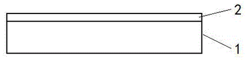
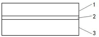
步骤S5,将(键合粘附在硅目标晶圆3上的)锗转移层2与锗供体晶圆1分离(即剥离,使用热、机械或其他合适的技术进行剥离),得到锗硅混合晶圆4(即锗转移层2和硅目标晶圆3所构成的混合晶圆)。图4为步骤S5的示意图。Step S5, the germanium transfer layer 2 (bonded and adhered to the silicon target wafer 3) is separated from the germanium donor wafer 1 (ie, peeled off, using thermal, mechanical or other suitable techniques for peeling off) to obtain germanium silicon Hybrid wafer 4 (ie, a hybrid wafer composed of
其中,剥离方法例如选择性剥离能量放置步骤(selective cleave energyplacement step),选择性剥离能量放置方法具体采用能量脉冲技术手段,能量脉冲就是通过提供局部(小范围内)能量脉冲,诸如采用热源(例如激光、加热灯)、冷源和机械源,从而实现例如扭转剥离;具体为加热(例如采用大约350摄氏度热源加热)或冷却或差异加热或差异冷却衬底(锗供体晶圆1或硅目标晶圆4)的一侧。在另外的实施例中,剥离方法再如离子注入气泡分离步骤(implantation blister-separation step),具体包括,将氢离子(H+)注入锗供体晶圆1,注入的氢离子捕获电子形成氢气,氢气在起泡层中形成微气泡层,平行于解理面(晶体的裂开面),加热锗硅混合晶圆4并沿解理面进行剥离;其中洁净步骤和自键合过程可参照前述贝塔键合中的过程。Among them, the exfoliation method such as the selective cleave energy placement step (selective cleave energy placement step), the selective exfoliation energy placement method specifically adopts the energy pulse technology means, and the energy pulse is provided by providing a local (small range) energy pulse, such as using a heat source (eg lasers, heat lamps), cold sources and mechanical sources to achieve e.g. torsional lift-off; specifically heating (e.g. with a heat source around 350 degrees Celsius) or cooling or differentially heating or differentially cooling the substrate (
可选地,对于分离后的锗供体晶圆1,通过研磨(化学机械研磨(CMP))表面并对表面进行洁净处理后,可重复使用;即反复使用一片锗供体晶圆1作为步骤S2的原料来产生锗转移层2,直至其厚度薄至无法继续使用。Optionally, the separated
步骤S6,完成锗硅混合晶圆4最终键合。In step S6, the final bonding of the germanium-silicon
最终键合步骤采用如下键合步骤,例如:键合步骤方法一,退火键合步骤,在小于或等于400摄氏度的工艺环境下持续数小时,优选地,在300摄氏度的工艺环境下持续3小时。键合步骤方法二,施加电压键合步骤,施加电压以建立通过混合晶圆的电流,限制晶圆中引入的晶体缺陷,电流加热并导致晶圆之间的键合,优选采用界面局部加热(增加串联电阻)进行键合。The final bonding step adopts the following bonding steps, for example: the
步骤S7,研磨锗硅混合晶圆4的锗转移层2的表面。其中,研磨例如采用化学机械研磨,具体地,浆液中含有温和的研磨剂和氧化剂(混合在去离子水中),研磨剂例如为硼硅酸盐玻璃、二氧化钛、氮化钛、氧化铝、三氧化铝、硝酸铁、氧化铈、二氧化硅(胶体二氧化硅或气相(微粉)二氧化硅)、氮化硅、碳化硅、石墨、金刚石,氧化剂例如为H2O2、KIO3、硝酸铁。In step S7 , the surface of the
可选地,在研磨后,可在锗硅混合晶圆4顶部的锗转移层2上沉积一层等离子增强化学气相沉积二氧化硅膜,以在随后硼离子注入期间保护锗转移层2的表面,并且该二氧化硅膜可在硼离子注入后移除。Optionally, after grinding, a plasma-enhanced chemical vapor deposition silicon dioxide film may be deposited on the
步骤S8,将掺杂元素离子硼离子(B+)注入锗硅混合晶圆4顶部的锗转移层2,使锗转移层2靠近表面的部分被注入硼而形成掺杂锗层5(p型区),其余部分(靠近硅目标晶圆3的部分)为未掺杂锗层6(硼离子无法到达,故无硼,为本征区)。随后进行退火以激活掺杂物。图5为步骤S8的示意图。其中,掺杂物也称掺杂剂、植入物等,为已注入的硼原子。In step S8 , boron ions (B + ) are implanted into the
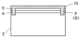
图6、图7所示为步骤S9的示意图,图6为步骤S9.1完成后状态的示意图,图7为步骤S9.3完成后状态的示意图。需要说明的是,图7至图17均为单个像素区域的放大视图,例如图6中A所示部分。FIG. 6 and FIG. 7 are schematic diagrams of step S9, FIG. 6 is a schematic diagram of a state after step S9.1 is completed, and FIG. 7 is a schematic diagram of a state after step S9.3 is completed. It should be noted that FIGS. 7 to 17 are all enlarged views of a single pixel area, such as the part shown in A in FIG. 6 .
步骤S9,在锗光电二极管层7中形成像素到像素之间的隔离结构,以界定光电二极管区域(即光电二极管阵列,亦即像素区域)。其中,如图6所示,锗光电二极管层7是指,依次相连接的掺杂锗层5、未掺杂锗层6以及一部分硅目标晶圆3,亦即在之后步骤中形成的锗p-i-n光电二极管层对应的部分。Step S9 , forming pixel-to-pixel isolation structures in the
步骤S9进一步包括:Step S9 further includes:
步骤S9.1,构成隔离图案并通过蚀刻形成隔离沟槽8,以定义(划分)每个像素区域;例如,如果所需构成的像素的形状为方形,则隔离图案类似于方形网格;使用光刻方法对该网格进行图形化,然后进行蚀刻以生成隔离沟槽8;Step S9.1, forming an isolation pattern and forming
步骤S9.2,用可流动的介电材料(例如聚酰亚胺)填充隔离沟槽8,形成沟槽间介电层9;Step S9.2, filling the
步骤S9.3,过量填充可流动的介电材料,使其填满隔离沟槽8后溢出,覆盖到像素区域,形成表面介电层10。In step S9.3, the flowable dielectric material is excessively filled so that it fills the
图8所示为步骤S10至步骤S11的示意图。FIG. 8 is a schematic diagram of steps S10 to S11.
步骤S10,翻转锗硅混合晶圆4。In step S10, the silicon-
步骤S11,提供一个涂布有临时黏合剂12的载体11。临时黏合剂12(temporarybonding adhesive)可采用现有技术,通过键合或粘合方式实现结合。In step S11, a
图9所示为步骤S12完成后状态的示意图。FIG. 9 is a schematic diagram of the state after step S12 is completed.
步骤S12,通过临时黏合剂12将锗硅混合晶圆4(具有可流动的介质材料的一面)临时键合/粘合到载体11上。In step S12 , the silicon-germanium hybrid wafer 4 (the side with the flowable dielectric material) is temporarily bonded/bonded to the
图10所示为步骤S13完成后状态的示意图。FIG. 10 is a schematic diagram showing the state after step S13 is completed.
步骤S13,通过研磨(如化学机械研磨或蚀刻(如湿法蚀刻)或其他合适的技术)去除大部分硅目标晶圆3(n型),直至像素隔离的底部13。从而,在未掺杂锗层6的顶部形成(保留)一层剩余硅层14(n型区),依次相连的剩余硅层14、未掺杂锗层6以及掺杂锗层5共同构成锗p-i-n光电二极管层(即锗光电二极管层7)。其中,像素隔离的底部13是指,沟槽间介电层9远离表面介电层10的一端所对应的层面,亦即根据需要/工艺要求所保留的剩余硅层14的研磨面所对应的层面。In step S13, most of the silicon target wafer 3 (n-type) is removed by grinding (eg, chemical mechanical polishing or etching (eg, wet etching) or other suitable techniques) until the bottom 13 of the pixel isolation. Therefore, a residual silicon layer 14 (n-type region) is formed (reserved) on top of the
图11所示为步骤S14完成后状态的示意图。FIG. 11 is a schematic diagram showing the state after step S14 is completed.
步骤S14,在剩余硅层14的朝外侧的表面沉积一层介电钝化层16。Step S14 , depositing a
图12所示为步骤S15完成后状态的示意图。FIG. 12 is a schematic diagram showing the state after step S15 is completed.
步骤S15,对剩余硅层14(n型区)和掺杂锗层5(p型区)分别单独形成金属连接15。In step S15 ,
步骤S15进一步包括:Step S15 further includes:
步骤S15.1,构成金属连接图案并蚀刻形成过孔至剩余硅层14(n型区)和掺杂锗层5(p型区)。通过物理气相沉积(PVD)在过孔的侧壁上形成阻挡金属(BM)和铜(Cu)籽晶,通过铜电化学沉积填充过孔,形成金属连接15。Step S15.1, forming metal connection patterns and etching via holes to the remaining silicon layer 14 (n-type region) and the doped germanium layer 5 (p-type region). Barrier metal (BM) and copper (Cu) seeds are formed on the sidewalls of the vias by physical vapor deposition (PVD), and the vias are filled by electrochemical deposition of copper to form
步骤S15.2,对表面进行研磨(例如化学机械研磨),去除多余的铜,露出铜垫和介质场,使金属连接15与介电钝化层16相齐平。其中,介电钝化层16可能在化学机械研磨后变薄。In step S15.2, the surface is ground (eg, chemical mechanical grinding) to remove excess copper, exposing the copper pad and the dielectric field, so that the
步骤S16,在介电钝化层16朝外侧的表面(通过任意合适的技术)形成对齐标记(alignment marks)。Step S16, forming alignment marks on the outer surface of the dielectric passivation layer 16 (by any suitable technique).
图13所示为步骤S17至步骤S18的示意图。FIG. 13 is a schematic diagram of steps S17 to S18.
步骤S17,提供硅控制和读出电路晶圆17。In step S17, silicon control and
其中,硅控制和读出电路晶圆17具有给于p-i-n光电二极管阵列层(即,锗光电二极管层7)的控制、读出和/或其他合适的电路,靠近外侧的表面为具有电路的互联层18,并且,互联层18朝外侧的表面为铜和阻挡金属化学机械研磨后形成的表面,即,表面暴露有电路金属触点(铜垫)。Among them, silicon control and
以及,步骤S17进一步包括:And, step S17 further comprises:
步骤S17.1,在互联层18朝外侧的表面(通过任意合适的技术)形成对齐标记。此对齐标记与步骤S16在介电钝化层16表面形成的对齐标记相匹配,从而在后续组合时实现辅助对齐的效果。Step S17.1, forming alignment marks on the outer surface of the interconnect layer 18 (by any suitable technique). This alignment mark matches the alignment mark formed on the surface of the
步骤S18,将硅控制和读出电路晶圆17的互联层18朝外侧的表面与(临时键合到载体11的)锗光电二极管层7的介电钝化层16朝外侧的表面相对接,通过二者上的对齐标记保证二者对齐,使锗光电二极管层7的金属连接15与互联层18的电路相连接。并在二者之间进行键合,例如混合键合(铜-铜键合和氧化物-氧化物键合)。铜-铜键合过程为,在铜晶粒生长过程中,通过铜的相互扩散来连接上侧的铜垫和下侧的铜垫(金属连接15和互联层18的电路相对接的两铜部分的界面)。In step S18, the outer-facing surface of the
其中,上述的对齐标记,也称对准标记,为现有技术。为了使器件能够工作,锗光电二极管层7的金属连接15与硅控制和读出电路晶圆17的互联层18的电路必须彼此对齐(电路相连通)。为此需要设置至少一组对齐标记,这些对齐标记是高精度特征,在组合定位时用作参考。对齐标记的设置根据现有技术即可实现,故本文不再赘述。The above-mentioned alignment marks, also called alignment marks, are in the prior art. For the device to work, the
图14所示为步骤S18完成后状态的示意图。FIG. 14 is a schematic diagram showing the state after step S18 is completed.
步骤S19,进行退火以完成键合。氧化物-氧化物键合过程为,退火时,通过脱水缩合反应连接上部和下部介质场(连接互联层18和介电钝化层16)。In step S19, annealing is performed to complete the bonding. The oxide-oxide bonding process is, upon annealing, connecting the upper and lower dielectric fields (connecting the
步骤S20,进行激光脱键/脱粘,移除载体11。In step S20 , laser debonding/debonding is performed to remove the
图15所示为步骤S20完成后状态的示意图。FIG. 15 is a schematic diagram showing the state after step S20 is completed.
步骤S21,通过研磨(通过例如化学机械研磨或其他合适的技术)去除表面介电层10。即,去除像素区域表面部分的可流动的介电材料(沟槽间介电层9仍存在),使掺杂锗层5暴露在表面。In step S21, the
图16所示为步骤S21完成后状态的示意图。FIG. 16 is a schematic diagram showing the state after step S21 is completed.
步骤S22,在表面(掺杂锗层5及沟槽间介电层9共同构成的表面)沉积抗反射层19。In step S22 , an
步骤S23,在抗反射层19顶部形成透镜层21。In step S23 , a
优选地,在抗反射层19顶部和透镜层21之间还形成有滤光层20。Preferably, a
图17所示为优选实施方式中步骤S22、步骤S23完成后状态的示意图,即为最终产品的结构示意图。FIG. 17 is a schematic diagram showing the state after steps S22 and S23 are completed in the preferred embodiment, that is, a schematic structural diagram of the final product.
方法B,磷掺杂锗(n型区)在顶部,掺杂锗层5为n型区,向锗中注入的掺杂元素离子为磷离子(P+),剩余硅层14为p型区。Method B, phosphorus doped germanium (n-type region) is on the top, the doped
与方法A的区别仅在于步骤S3提供的硅目标晶圆3为p型,从而剩余硅层14为p型区;步骤S8中注入的掺杂元素离子为磷离子(P+),所形成的掺杂锗层5为n型区,其余所用工艺及操作过程均与方法A相同。The only difference from method A is that the
如本领域所公知的,在Ⅳ族的元素(例如锗)中掺杂Ⅲ族的元素(例如硼),则形成p型半导体;在Ⅳ族的元素(例如锗)中掺杂Ⅴ族的元素(例如磷),则形成n型半导体。因此,通过本发明上文详细介绍的方法A得到这些类似的变体方法是显而易见的。As is known in the art, doping a group IV element (such as germanium) with a group III element (such as boron) forms a p-type semiconductor; doping a group IV element (such as germanium) with a group V element (for example, phosphorus), an n-type semiconductor is formed. Accordingly, it is apparent that these analogous variant methods are obtained by the method A of the present invention detailed above.
综上所述,本发明以低成本、相对更简单的制造工艺实现了高速、小像素尺寸、CMOS兼容的短波红外图像传感器(具有焦平面阵列),适于工业化大规模生产。同时,采用本发明的方法所制造的图像传感器从可见光到短波红外波长的暗电流更低、灵敏度更高。此外,本发明的方法中,锗供体晶圆可重复利用以产生更多锗转移层,资源利用率更高,制造成本更低。To sum up, the present invention realizes a high-speed, small pixel size, CMOS-compatible short-wave infrared image sensor (with a focal plane array) with a low-cost and relatively simpler manufacturing process, which is suitable for industrial mass production. Meanwhile, the image sensor manufactured by the method of the present invention has lower dark current and higher sensitivity from visible light to short-wave infrared wavelengths. In addition, in the method of the present invention, the germanium donor wafer can be reused to generate more germanium transfer layers, the resource utilization rate is higher, and the manufacturing cost is lower.
以上所述,仅为本发明较佳的具体实施方式,但本发明的保护范围并不局限于此,任何熟悉本技术领域的技术人员在本发明揭露的技术范围内,可轻易想到的变化或替换,都应涵盖在本发明的保护范围之内。本领域普通的技术人员可以理解,在不背离所附权利要求定义的本发明的精神和范围的情况下,可以在形式和细节中做出各种各样的修改。The above description is only a preferred embodiment of the present invention, but the protection scope of the present invention is not limited to this. Substitutions should be covered within the protection scope of the present invention. It will be understood by those of ordinary skill in the art that various changes in form and details may be made therein without departing from the spirit and scope of the present invention as defined by the appended claims.
Claims (12)
Priority Applications (1)
| Application Number | Priority Date | Filing Date | Title |
|---|---|---|---|
| CN202210504638.3A CN114709233B (en) | 2022-05-10 | 2022-05-10 | A method for integrating germanium p-i-n photodiodes into image sensor structures |
Applications Claiming Priority (1)
| Application Number | Priority Date | Filing Date | Title |
|---|---|---|---|
| CN202210504638.3A CN114709233B (en) | 2022-05-10 | 2022-05-10 | A method for integrating germanium p-i-n photodiodes into image sensor structures |
Publications (2)
| Publication Number | Publication Date |
|---|---|
| CN114709233A true CN114709233A (en) | 2022-07-05 |
| CN114709233B CN114709233B (en) | 2025-06-03 |
Family
ID=82176669
Family Applications (1)
| Application Number | Title | Priority Date | Filing Date |
|---|---|---|---|
| CN202210504638.3A Active CN114709233B (en) | 2022-05-10 | 2022-05-10 | A method for integrating germanium p-i-n photodiodes into image sensor structures |
Country Status (1)
| Country | Link |
|---|---|
| CN (1) | CN114709233B (en) |
Citations (3)
| Publication number | Priority date | Publication date | Assignee | Title |
|---|---|---|---|---|
| CN104752341A (en) * | 2013-12-31 | 2015-07-01 | 上海丽恒光微电子科技有限公司 | Infrared avalanche diode array device, forming method and laser three-dimensional imaging device |
| CN110663114A (en) * | 2017-04-13 | 2020-01-07 | 奥特逻科公司 | Germanium-silicon light sensing device II |
| CN112216767A (en) * | 2019-07-09 | 2021-01-12 | 原子能与替代能源委员会 | Fabrication of semiconductor photosensitive devices |
-
2022
- 2022-05-10 CN CN202210504638.3A patent/CN114709233B/en active Active
Patent Citations (4)
| Publication number | Priority date | Publication date | Assignee | Title |
|---|---|---|---|---|
| CN104752341A (en) * | 2013-12-31 | 2015-07-01 | 上海丽恒光微电子科技有限公司 | Infrared avalanche diode array device, forming method and laser three-dimensional imaging device |
| CN110663114A (en) * | 2017-04-13 | 2020-01-07 | 奥特逻科公司 | Germanium-silicon light sensing device II |
| CN112216767A (en) * | 2019-07-09 | 2021-01-12 | 原子能与替代能源委员会 | Fabrication of semiconductor photosensitive devices |
| US20210013361A1 (en) * | 2019-07-09 | 2021-01-14 | Commissariat à I'Energie Atomique et aux Energies Alternatives | Manufacturing of a semiconductor photosensitive device |
Also Published As
| Publication number | Publication date |
|---|---|
| CN114709233B (en) | 2025-06-03 |
Similar Documents
| Publication | Publication Date | Title |
|---|---|---|
| JP5367562B2 (en) | Manufacturing method and structure of solar cell | |
| US8865507B2 (en) | Integrated visible and infrared imager devices and associated methods | |
| US7276429B2 (en) | Method and apparatus for producing ultra-thin semiconductor chip and method and apparatus for producing ultra-thin back-illuminated solid-state image pickup device | |
| US7759220B2 (en) | Method and structure for fabricating solar cells using a layer transfer process | |
| CN102947953A (en) | Device and associated method with enhanced detection of electromagnetic radiation | |
| JP2005514795A (en) | Photovoltaic cell and method for producing photovoltaic cell | |
| US20110174376A1 (en) | Monocrystalline Thin Cell | |
| CN108630781B (en) | 3-5 mu m infrared band avalanche photodiode detector and manufacturing method thereof | |
| CN217158212U (en) | Image sensor based on germanium p-i-n photodiode | |
| CN116885040A (en) | Photodetector device and preparation method thereof | |
| CN104205364B (en) | The manufacture of multijunction solar cell device | |
| CN114597226B (en) | A kind of manufacturing method of image sensor based on germanium p-i-n photodiode | |
| CN114709233B (en) | A method for integrating germanium p-i-n photodiodes into image sensor structures | |
| CN217158193U (en) | Image sensor | |
| CN217158210U (en) | Image sensor manufactured based on germanium p-i-n photodiode | |
| JP2005268238A (en) | Back-illuminated solid-state imaging device and manufacturing method thereof | |
| CN217158211U (en) | Image sensor based on germanium p-i-n photodiode | |
| US8871608B2 (en) | Method for fabricating backside-illuminated sensors | |
| CN116583953B (en) | Method for forming semiconductor structure | |
| CN115000101A (en) | A method of forming germanium devices on silicon | |
| WO2013019250A1 (en) | A photovoltaic device and a process for producing a photovoltaic device | |
| KR100993846B1 (en) | Solar cell, manufacturing method thereof and solar cell manufacturing apparatus for manufacturing same | |
| CN113540140A (en) | Backside illuminated complementary metal oxide semiconductor image sensor and preparation method thereof | |
| Fedeli et al. | Photonics and electronics integration in the HELIOS project | |
| CN117373915B (en) | Semiconductor structure thinning method and structure |
Legal Events
| Date | Code | Title | Description |
|---|---|---|---|
| PB01 | Publication | ||
| PB01 | Publication | ||
| SE01 | Entry into force of request for substantive examination | ||
| SE01 | Entry into force of request for substantive examination | ||
| GR01 | Patent grant | ||
| GR01 | Patent grant |