CN1237140C - Composition and method for sealing microcups in roll-to-roll display manufacturing - Google Patents
Composition and method for sealing microcups in roll-to-roll display manufacturing Download PDFInfo
- Publication number
- CN1237140C CN1237140C CNB011364483A CN01136448A CN1237140C CN 1237140 C CN1237140 C CN 1237140C CN B011364483 A CNB011364483 A CN B011364483A CN 01136448 A CN01136448 A CN 01136448A CN 1237140 C CN1237140 C CN 1237140C
- Authority
- CN
- China
- Prior art keywords
- poly
- vinylbenzene
- solvent
- alpha
- methyl styrene
- Prior art date
- Legal status (The legal status is an assumption and is not a legal conclusion. Google has not performed a legal analysis and makes no representation as to the accuracy of the status listed.)
- Expired - Lifetime
Links
- 238000000034 method Methods 0.000 title claims abstract description 92
- 238000007789 sealing Methods 0.000 title claims abstract description 55
- 239000000203 mixture Substances 0.000 title claims description 21
- 238000004519 manufacturing process Methods 0.000 title description 20
- 239000004973 liquid crystal related substance Substances 0.000 claims abstract description 13
- 239000002904 solvent Substances 0.000 claims description 75
- 239000012530 fluid Substances 0.000 claims description 44
- -1 propylene, butylene Chemical group 0.000 claims description 29
- 229920002725 thermoplastic elastomer Polymers 0.000 claims description 29
- PPBRXRYQALVLMV-UHFFFAOYSA-N Styrene Chemical compound C=CC1=CC=CC=C1 PPBRXRYQALVLMV-UHFFFAOYSA-N 0.000 claims description 28
- YXFVVABEGXRONW-UHFFFAOYSA-N Toluene Chemical compound CC1=CC=CC=C1 YXFVVABEGXRONW-UHFFFAOYSA-N 0.000 claims description 27
- IMNFDUFMRHMDMM-UHFFFAOYSA-N N-Heptane Chemical compound CCCCCCC IMNFDUFMRHMDMM-UHFFFAOYSA-N 0.000 claims description 22
- 238000000576 coating method Methods 0.000 claims description 18
- 239000003795 chemical substances by application Substances 0.000 claims description 16
- 239000011877 solvent mixture Substances 0.000 claims description 14
- CTQNGGLPUBDAKN-UHFFFAOYSA-N O-Xylene Chemical compound CC1=CC=CC=C1C CTQNGGLPUBDAKN-UHFFFAOYSA-N 0.000 claims description 13
- 239000011248 coating agent Substances 0.000 claims description 13
- 238000002360 preparation method Methods 0.000 claims description 12
- 239000004094 surface-active agent Substances 0.000 claims description 11
- KAKZBPTYRLMSJV-UHFFFAOYSA-N Butadiene Chemical group C=CC=C KAKZBPTYRLMSJV-UHFFFAOYSA-N 0.000 claims description 8
- 229920002943 EPDM rubber Polymers 0.000 claims description 8
- RRHGJUQNOFWUDK-UHFFFAOYSA-N Isoprene Chemical group CC(=C)C=C RRHGJUQNOFWUDK-UHFFFAOYSA-N 0.000 claims description 8
- NNBZCPXTIHJBJL-UHFFFAOYSA-N decalin Chemical compound C1CCCC2CCCCC21 NNBZCPXTIHJBJL-UHFFFAOYSA-N 0.000 claims description 8
- BKIMMITUMNQMOS-UHFFFAOYSA-N nonane Chemical compound CCCCCCCCC BKIMMITUMNQMOS-UHFFFAOYSA-N 0.000 claims description 8
- 239000012815 thermoplastic material Substances 0.000 claims description 8
- 150000001335 aliphatic alkanes Chemical class 0.000 claims description 7
- 150000004996 alkyl benzenes Chemical class 0.000 claims description 7
- VGGSQFUCUMXWEO-UHFFFAOYSA-N Ethene Chemical compound C=C VGGSQFUCUMXWEO-UHFFFAOYSA-N 0.000 claims description 6
- 239000005977 Ethylene Substances 0.000 claims description 6
- 125000005907 alkyl ester group Chemical group 0.000 claims description 6
- 239000000080 wetting agent Substances 0.000 claims description 6
- 239000004793 Polystyrene Substances 0.000 claims description 5
- XYLMUPLGERFSHI-UHFFFAOYSA-N alpha-Methylstyrene Chemical compound CC(=C)C1=CC=CC=C1 XYLMUPLGERFSHI-UHFFFAOYSA-N 0.000 claims description 5
- 229920000578 graft copolymer Polymers 0.000 claims description 5
- 229920002223 polystyrene Polymers 0.000 claims description 5
- MBNVSWHUJDDZRH-UHFFFAOYSA-N 2-methylthiirane Chemical group CC1CS1 MBNVSWHUJDDZRH-UHFFFAOYSA-N 0.000 claims description 4
- XDTMQSROBMDMFD-UHFFFAOYSA-N Cyclohexane Chemical compound C1CCCCC1 XDTMQSROBMDMFD-UHFFFAOYSA-N 0.000 claims description 4
- LFQSCWFLJHTTHZ-UHFFFAOYSA-N Ethanol Chemical compound CCO LFQSCWFLJHTTHZ-UHFFFAOYSA-N 0.000 claims description 4
- 239000000178 monomer Substances 0.000 claims description 4
- TVMXDCGIABBOFY-UHFFFAOYSA-N octane Chemical compound CCCCCCCC TVMXDCGIABBOFY-UHFFFAOYSA-N 0.000 claims description 4
- 125000005233 alkylalcohol group Chemical group 0.000 claims description 3
- 238000001035 drying Methods 0.000 claims description 3
- 229930195733 hydrocarbon Natural products 0.000 claims description 3
- 150000002430 hydrocarbons Chemical class 0.000 claims description 3
- 239000003999 initiator Substances 0.000 claims description 3
- 229920001296 polysiloxane Polymers 0.000 claims description 3
- KUAZQDVKQLNFPE-UHFFFAOYSA-N thiram Chemical compound CN(C)C(=S)SSC(=S)N(C)C KUAZQDVKQLNFPE-UHFFFAOYSA-N 0.000 claims description 3
- 229960002447 thiram Drugs 0.000 claims description 3
- 239000013543 active substance Substances 0.000 claims 4
- 239000004215 Carbon black (E152) Substances 0.000 claims 2
- BAPJBEWLBFYGME-UHFFFAOYSA-N Methyl acrylate Chemical class COC(=O)C=C BAPJBEWLBFYGME-UHFFFAOYSA-N 0.000 claims 2
- UHOVQNZJYSORNB-UHFFFAOYSA-N benzene Substances C1=CC=CC=C1 UHOVQNZJYSORNB-UHFFFAOYSA-N 0.000 claims 2
- 150000001732 carboxylic acid derivatives Chemical class 0.000 claims 2
- 239000003153 chemical reaction reagent Substances 0.000 claims 2
- 125000001153 fluoro group Chemical group F* 0.000 claims 2
- 125000005574 norbornylene group Chemical group 0.000 claims 2
- 229920003251 poly(α-methylstyrene) Polymers 0.000 claims 2
- QQONPFPTGQHPMA-UHFFFAOYSA-N propylene Natural products CC=C QQONPFPTGQHPMA-UHFFFAOYSA-N 0.000 claims 2
- 125000004805 propylene group Chemical group [H]C([H])([H])C([H])([*:1])C([H])([H])[*:2] 0.000 claims 2
- 238000001259 photo etching Methods 0.000 claims 1
- 239000000463 material Substances 0.000 abstract description 25
- 230000007547 defect Effects 0.000 abstract description 2
- 210000004027 cell Anatomy 0.000 abstract 1
- 210000002858 crystal cell Anatomy 0.000 abstract 1
- 239000003566 sealing material Substances 0.000 abstract 1
- 239000000049 pigment Substances 0.000 description 57
- 239000002245 particle Substances 0.000 description 47
- 239000010410 layer Substances 0.000 description 29
- 230000005855 radiation Effects 0.000 description 24
- 239000000758 substrate Substances 0.000 description 23
- 230000008569 process Effects 0.000 description 22
- ZWEHNKRNPOVVGH-UHFFFAOYSA-N 2-Butanone Chemical compound CCC(C)=O ZWEHNKRNPOVVGH-UHFFFAOYSA-N 0.000 description 15
- 239000000725 suspension Substances 0.000 description 14
- 238000003491 array Methods 0.000 description 13
- 239000003094 microcapsule Substances 0.000 description 13
- 229920002120 photoresistant polymer Polymers 0.000 description 13
- 239000002243 precursor Substances 0.000 description 12
- 239000003086 colorant Substances 0.000 description 10
- 239000006185 dispersion Substances 0.000 description 10
- 239000000975 dye Substances 0.000 description 10
- KFZMGEQAYNKOFK-UHFFFAOYSA-N Isopropanol Chemical compound CC(C)O KFZMGEQAYNKOFK-UHFFFAOYSA-N 0.000 description 9
- 238000011049 filling Methods 0.000 description 9
- 239000000126 substance Substances 0.000 description 9
- 230000005484 gravity Effects 0.000 description 7
- 239000004033 plastic Substances 0.000 description 7
- 229920003023 plastic Polymers 0.000 description 7
- 239000011347 resin Substances 0.000 description 7
- 229920005989 resin Polymers 0.000 description 7
- 229920001169 thermoplastic Polymers 0.000 description 7
- 239000004416 thermosoftening plastic Substances 0.000 description 7
- XEKOWRVHYACXOJ-UHFFFAOYSA-N Ethyl acetate Chemical compound CCOC(C)=O XEKOWRVHYACXOJ-UHFFFAOYSA-N 0.000 description 6
- 229920002633 Kraton (polymer) Polymers 0.000 description 6
- GWEVSGVZZGPLCZ-UHFFFAOYSA-N Titan oxide Chemical compound O=[Ti]=O GWEVSGVZZGPLCZ-UHFFFAOYSA-N 0.000 description 6
- 229920001577 copolymer Polymers 0.000 description 6
- 230000003287 optical effect Effects 0.000 description 6
- 229920000642 polymer Polymers 0.000 description 6
- 229920001187 thermosetting polymer Polymers 0.000 description 6
- 238000009736 wetting Methods 0.000 description 6
- CSCPPACGZOOCGX-UHFFFAOYSA-N Acetone Chemical compound CC(C)=O CSCPPACGZOOCGX-UHFFFAOYSA-N 0.000 description 5
- 230000004888 barrier function Effects 0.000 description 5
- 238000001053 micromoulding Methods 0.000 description 5
- 238000000206 photolithography Methods 0.000 description 5
- 238000012545 processing Methods 0.000 description 5
- 239000008096 xylene Substances 0.000 description 5
- PXHVJJICTQNCMI-UHFFFAOYSA-N Nickel Chemical compound [Ni] PXHVJJICTQNCMI-UHFFFAOYSA-N 0.000 description 4
- 239000004020 conductor Substances 0.000 description 4
- 238000001723 curing Methods 0.000 description 4
- 150000001924 cycloalkanes Chemical class 0.000 description 4
- DIOQZVSQGTUSAI-UHFFFAOYSA-N decane Chemical compound CCCCCCCCCC DIOQZVSQGTUSAI-UHFFFAOYSA-N 0.000 description 4
- 238000010586 diagram Methods 0.000 description 4
- 229920001971 elastomer Polymers 0.000 description 4
- 238000003475 lamination Methods 0.000 description 4
- 229910052751 metal Inorganic materials 0.000 description 4
- 239000002184 metal Substances 0.000 description 4
- 239000003921 oil Substances 0.000 description 4
- 229920001195 polyisoprene Polymers 0.000 description 4
- 239000005060 rubber Substances 0.000 description 4
- 238000000935 solvent evaporation Methods 0.000 description 4
- 229920001935 styrene-ethylene-butadiene-styrene Polymers 0.000 description 4
- YIKSHDNOAYSSPX-UHFFFAOYSA-N 1-propan-2-ylthioxanthen-9-one Chemical compound S1C2=CC=CC=C2C(=O)C2=C1C=CC=C2C(C)C YIKSHDNOAYSSPX-UHFFFAOYSA-N 0.000 description 3
- OKTJSMMVPCPJKN-UHFFFAOYSA-N Carbon Chemical compound [C] OKTJSMMVPCPJKN-UHFFFAOYSA-N 0.000 description 3
- 239000004971 Cross linker Substances 0.000 description 3
- 230000001070 adhesive effect Effects 0.000 description 3
- PYKYMHQGRFAEBM-UHFFFAOYSA-N anthraquinone Natural products CCC(=O)c1c(O)c2C(=O)C3C(C=CC=C3O)C(=O)c2cc1CC(=O)OC PYKYMHQGRFAEBM-UHFFFAOYSA-N 0.000 description 3
- 150000004056 anthraquinones Chemical class 0.000 description 3
- 230000008901 benefit Effects 0.000 description 3
- 238000011161 development Methods 0.000 description 3
- 230000018109 developmental process Effects 0.000 description 3
- 229920000359 diblock copolymer Polymers 0.000 description 3
- 238000005323 electroforming Methods 0.000 description 3
- 238000009713 electroplating Methods 0.000 description 3
- 238000010030 laminating Methods 0.000 description 3
- 230000004048 modification Effects 0.000 description 3
- 238000012986 modification Methods 0.000 description 3
- 229920002037 poly(vinyl butyral) polymer Polymers 0.000 description 3
- 229920000139 polyethylene terephthalate Polymers 0.000 description 3
- 239000005020 polyethylene terephthalate Substances 0.000 description 3
- 238000006116 polymerization reaction Methods 0.000 description 3
- YCUVUDODLRLVIC-VPHDGDOJSA-N sudan black b Chemical compound C1=CC(=C23)NC(C)(C)NC2=CC=CC3=C1\N=N\C(C1=CC=CC=C11)=CC=C1\N=N\C1=CC=CC=C1 YCUVUDODLRLVIC-VPHDGDOJSA-N 0.000 description 3
- 229920000428 triblock copolymer Polymers 0.000 description 3
- MYRTYDVEIRVNKP-UHFFFAOYSA-N 1,2-Divinylbenzene Chemical compound C=CC1=CC=CC=C1C=C MYRTYDVEIRVNKP-UHFFFAOYSA-N 0.000 description 2
- MLIWQXBKMZNZNF-UHFFFAOYSA-N 2,6-bis[(4-azidophenyl)methylidene]-4-methylcyclohexan-1-one Chemical compound O=C1C(=CC=2C=CC(=CC=2)N=[N+]=[N-])CC(C)CC1=CC1=CC=C(N=[N+]=[N-])C=C1 MLIWQXBKMZNZNF-UHFFFAOYSA-N 0.000 description 2
- 229920002799 BoPET Polymers 0.000 description 2
- 238000012695 Interfacial polymerization Methods 0.000 description 2
- ATUOYWHBWRKTHZ-UHFFFAOYSA-N Propane Chemical compound CCC ATUOYWHBWRKTHZ-UHFFFAOYSA-N 0.000 description 2
- 238000003848 UV Light-Curing Methods 0.000 description 2
- 239000000853 adhesive Substances 0.000 description 2
- 239000012790 adhesive layer Substances 0.000 description 2
- 125000000217 alkyl group Chemical group 0.000 description 2
- JXLHNMVSKXFWAO-UHFFFAOYSA-N azane;7-fluoro-2,1,3-benzoxadiazole-4-sulfonic acid Chemical compound N.OS(=O)(=O)C1=CC=C(F)C2=NON=C12 JXLHNMVSKXFWAO-UHFFFAOYSA-N 0.000 description 2
- 238000000498 ball milling Methods 0.000 description 2
- 229910052799 carbon Inorganic materials 0.000 description 2
- 238000006243 chemical reaction Methods 0.000 description 2
- 239000000039 congener Substances 0.000 description 2
- 238000009826 distribution Methods 0.000 description 2
- 238000001312 dry etching Methods 0.000 description 2
- 230000005684 electric field Effects 0.000 description 2
- 238000010894 electron beam technology Methods 0.000 description 2
- 238000001962 electrophoresis Methods 0.000 description 2
- 238000004945 emulsification Methods 0.000 description 2
- 150000008282 halocarbons Chemical class 0.000 description 2
- 238000011065 in-situ storage Methods 0.000 description 2
- 239000004615 ingredient Substances 0.000 description 2
- 238000010406 interfacial reaction Methods 0.000 description 2
- GJRQTCIYDGXPES-UHFFFAOYSA-N iso-butyl acetate Natural products CC(C)COC(C)=O GJRQTCIYDGXPES-UHFFFAOYSA-N 0.000 description 2
- FGKJLKRYENPLQH-UHFFFAOYSA-M isocaproate Chemical compound CC(C)CCC([O-])=O FGKJLKRYENPLQH-UHFFFAOYSA-M 0.000 description 2
- OQAGVSWESNCJJT-UHFFFAOYSA-N isovaleric acid methyl ester Natural products COC(=O)CC(C)C OQAGVSWESNCJJT-UHFFFAOYSA-N 0.000 description 2
- 239000006233 lamp black Substances 0.000 description 2
- 239000007788 liquid Substances 0.000 description 2
- 238000000465 moulding Methods 0.000 description 2
- 229920006030 multiblock copolymer Polymers 0.000 description 2
- 229910052759 nickel Inorganic materials 0.000 description 2
- JFNLZVQOOSMTJK-KNVOCYPGSA-N norbornene Chemical compound C1[C@@H]2CC[C@H]1C=C2 JFNLZVQOOSMTJK-KNVOCYPGSA-N 0.000 description 2
- RNVCVTLRINQCPJ-UHFFFAOYSA-N o-toluidine Chemical compound CC1=CC=CC=C1N RNVCVTLRINQCPJ-UHFFFAOYSA-N 0.000 description 2
- 229920002493 poly(chlorotrifluoroethylene) Polymers 0.000 description 2
- 229920002492 poly(sulfone) Polymers 0.000 description 2
- 239000005023 polychlorotrifluoroethylene (PCTFE) polymer Substances 0.000 description 2
- 238000011417 postcuring Methods 0.000 description 2
- 239000000843 powder Substances 0.000 description 2
- 238000003847 radiation curing Methods 0.000 description 2
- 229960001860 salicylate Drugs 0.000 description 2
- 239000000565 sealant Substances 0.000 description 2
- 238000004062 sedimentation Methods 0.000 description 2
- KZNICNPSHKQLFF-UHFFFAOYSA-N succinimide Chemical compound O=C1CCC(=O)N1 KZNICNPSHKQLFF-UHFFFAOYSA-N 0.000 description 2
- 230000001360 synchronised effect Effects 0.000 description 2
- 238000012546 transfer Methods 0.000 description 2
- 230000007704 transition Effects 0.000 description 2
- PXXNTAGJWPJAGM-UHFFFAOYSA-N vertaline Natural products C1C2C=3C=C(OC)C(OC)=CC=3OC(C=C3)=CC=C3CCC(=O)OC1CC1N2CCCC1 PXXNTAGJWPJAGM-UHFFFAOYSA-N 0.000 description 2
- OJOWICOBYCXEKR-APPZFPTMSA-N (1S,4R)-5-ethylidenebicyclo[2.2.1]hept-2-ene Chemical compound CC=C1C[C@@H]2C[C@@H]1C=C2 OJOWICOBYCXEKR-APPZFPTMSA-N 0.000 description 1
- XEMRAKSQROQPBR-UHFFFAOYSA-N (trichloromethyl)benzene Chemical compound ClC(Cl)(Cl)C1=CC=CC=C1 XEMRAKSQROQPBR-UHFFFAOYSA-N 0.000 description 1
- FBTKIMWGAQACHU-UHFFFAOYSA-N 1,1-dichlorononane Chemical compound CCCCCCCCC(Cl)Cl FBTKIMWGAQACHU-UHFFFAOYSA-N 0.000 description 1
- BJYHBJUWZMHGGQ-UHFFFAOYSA-N 1,2-dichloro-3-(trifluoromethyl)benzene Chemical compound FC(F)(F)C1=CC=CC(Cl)=C1Cl BJYHBJUWZMHGGQ-UHFFFAOYSA-N 0.000 description 1
- OCQDPIXQTSYZJL-UHFFFAOYSA-N 1,4-bis(butylamino)anthracene-9,10-dione Chemical compound O=C1C2=CC=CC=C2C(=O)C2=C1C(NCCCC)=CC=C2NCCCC OCQDPIXQTSYZJL-UHFFFAOYSA-N 0.000 description 1
- ARKQRZXCXIMZHG-UHFFFAOYSA-N 1-azido-4-[(4-azidophenyl)methyl]benzene Chemical compound C1=CC(N=[N+]=[N-])=CC=C1CC1=CC=C(N=[N+]=[N-])C=C1 ARKQRZXCXIMZHG-UHFFFAOYSA-N 0.000 description 1
- KGCDGLXSBHJAHZ-UHFFFAOYSA-N 1-chloro-2,3,4,5,6-pentafluorobenzene Chemical compound FC1=C(F)C(F)=C(Cl)C(F)=C1F KGCDGLXSBHJAHZ-UHFFFAOYSA-N 0.000 description 1
- KWVGIHKZDCUPEU-UHFFFAOYSA-N 2,2-dimethoxy-2-phenylacetophenone Chemical compound C=1C=CC=CC=1C(OC)(OC)C(=O)C1=CC=CC=C1 KWVGIHKZDCUPEU-UHFFFAOYSA-N 0.000 description 1
- MFYSUUPKMDJYPF-UHFFFAOYSA-N 2-[(4-methyl-2-nitrophenyl)diazenyl]-3-oxo-n-phenylbutanamide Chemical compound C=1C=CC=CC=1NC(=O)C(C(=O)C)N=NC1=CC=C(C)C=C1[N+]([O-])=O MFYSUUPKMDJYPF-UHFFFAOYSA-N 0.000 description 1
- IAFBRPFISOTXSO-UHFFFAOYSA-N 2-[[2-chloro-4-[3-chloro-4-[[1-(2,4-dimethylanilino)-1,3-dioxobutan-2-yl]diazenyl]phenyl]phenyl]diazenyl]-n-(2,4-dimethylphenyl)-3-oxobutanamide Chemical compound C=1C=C(C)C=C(C)C=1NC(=O)C(C(=O)C)N=NC(C(=C1)Cl)=CC=C1C(C=C1Cl)=CC=C1N=NC(C(C)=O)C(=O)NC1=CC=C(C)C=C1C IAFBRPFISOTXSO-UHFFFAOYSA-N 0.000 description 1
- UHFFVFAKEGKNAQ-UHFFFAOYSA-N 2-benzyl-2-(dimethylamino)-1-(4-morpholin-4-ylphenyl)butan-1-one Chemical compound C=1C=C(N2CCOCC2)C=CC=1C(=O)C(CC)(N(C)C)CC1=CC=CC=C1 UHFFVFAKEGKNAQ-UHFFFAOYSA-N 0.000 description 1
- FIHBHSQYSYVZQE-UHFFFAOYSA-N 6-prop-2-enoyloxyhexyl prop-2-enoate Chemical compound C=CC(=O)OCCCCCCOC(=O)C=C FIHBHSQYSYVZQE-UHFFFAOYSA-N 0.000 description 1
- 229920002126 Acrylic acid copolymer Polymers 0.000 description 1
- 239000004342 Benzoyl peroxide Substances 0.000 description 1
- OMPJBNCRMGITSC-UHFFFAOYSA-N Benzoylperoxide Chemical compound C=1C=CC=CC=1C(=O)OOC(=O)C1=CC=CC=C1 OMPJBNCRMGITSC-UHFFFAOYSA-N 0.000 description 1
- OYPRJOBELJOOCE-UHFFFAOYSA-N Calcium Chemical compound [Ca] OYPRJOBELJOOCE-UHFFFAOYSA-N 0.000 description 1
- 229910000531 Co alloy Inorganic materials 0.000 description 1
- 229910021594 Copper(II) fluoride Inorganic materials 0.000 description 1
- 239000004593 Epoxy Substances 0.000 description 1
- 239000004831 Hot glue Substances 0.000 description 1
- YIVJZNGAASQVEM-UHFFFAOYSA-N Lauroyl peroxide Chemical compound CCCCCCCCCCCC(=O)OOC(=O)CCCCCCCCCCC YIVJZNGAASQVEM-UHFFFAOYSA-N 0.000 description 1
- CERQOIWHTDAKMF-UHFFFAOYSA-N Methacrylic acid Chemical compound CC(=C)C(O)=O CERQOIWHTDAKMF-UHFFFAOYSA-N 0.000 description 1
- 229910017709 Ni Co Inorganic materials 0.000 description 1
- 229910003267 Ni-Co Inorganic materials 0.000 description 1
- 229910003262 Ni‐Co Inorganic materials 0.000 description 1
- 239000005662 Paraffin oil Substances 0.000 description 1
- 239000004642 Polyimide Substances 0.000 description 1
- 239000004820 Pressure-sensitive adhesive Substances 0.000 description 1
- NRCMAYZCPIVABH-UHFFFAOYSA-N Quinacridone Chemical compound N1C2=CC=CC=C2C(=O)C2=C1C=C1C(=O)C3=CC=CC=C3NC1=C2 NRCMAYZCPIVABH-UHFFFAOYSA-N 0.000 description 1
- 229910010413 TiO 2 Inorganic materials 0.000 description 1
- HCHKCACWOHOZIP-UHFFFAOYSA-N Zinc Chemical compound [Zn] HCHKCACWOHOZIP-UHFFFAOYSA-N 0.000 description 1
- ZZAGLMPBQOKGGT-UHFFFAOYSA-N [4-[4-(4-prop-2-enoyloxybutoxy)benzoyl]oxyphenyl] 4-(4-prop-2-enoyloxybutoxy)benzoate Chemical class C1=CC(OCCCCOC(=O)C=C)=CC=C1C(=O)OC(C=C1)=CC=C1OC(=O)C1=CC=C(OCCCCOC(=O)C=C)C=C1 ZZAGLMPBQOKGGT-UHFFFAOYSA-N 0.000 description 1
- QXZUUHYBWMWJHK-UHFFFAOYSA-N [Co].[Ni] Chemical compound [Co].[Ni] QXZUUHYBWMWJHK-UHFFFAOYSA-N 0.000 description 1
- 150000001252 acrylic acid derivatives Chemical class 0.000 description 1
- 239000000654 additive Substances 0.000 description 1
- 230000002411 adverse Effects 0.000 description 1
- 239000000443 aerosol Substances 0.000 description 1
- 238000005054 agglomeration Methods 0.000 description 1
- 230000002776 aggregation Effects 0.000 description 1
- 150000001298 alcohols Chemical class 0.000 description 1
- 239000001000 anthraquinone dye Substances 0.000 description 1
- 238000000149 argon plasma sintering Methods 0.000 description 1
- 150000004945 aromatic hydrocarbons Chemical class 0.000 description 1
- 229920003235 aromatic polyamide Polymers 0.000 description 1
- 239000000987 azo dye Substances 0.000 description 1
- 125000000751 azo group Chemical group [*]N=N[*] 0.000 description 1
- 238000010923 batch production Methods 0.000 description 1
- 238000005452 bending Methods 0.000 description 1
- 230000009286 beneficial effect Effects 0.000 description 1
- 235000019400 benzoyl peroxide Nutrition 0.000 description 1
- 230000015572 biosynthetic process Effects 0.000 description 1
- 238000009835 boiling Methods 0.000 description 1
- 229910052791 calcium Inorganic materials 0.000 description 1
- 239000011575 calcium Substances 0.000 description 1
- 239000002775 capsule Substances 0.000 description 1
- 239000006229 carbon black Substances 0.000 description 1
- 150000001735 carboxylic acids Chemical class 0.000 description 1
- 239000000919 ceramic Substances 0.000 description 1
- 238000003486 chemical etching Methods 0.000 description 1
- 238000005354 coacervation Methods 0.000 description 1
- 238000005345 coagulation Methods 0.000 description 1
- 230000015271 coagulation Effects 0.000 description 1
- 239000008199 coating composition Substances 0.000 description 1
- 239000011247 coating layer Substances 0.000 description 1
- 150000001875 compounds Chemical class 0.000 description 1
- 238000000748 compression moulding Methods 0.000 description 1
- 238000010924 continuous production Methods 0.000 description 1
- 238000001816 cooling Methods 0.000 description 1
- 238000007334 copolymerization reaction Methods 0.000 description 1
- XCJYREBRNVKWGJ-UHFFFAOYSA-N copper(II) phthalocyanine Chemical compound [Cu+2].C12=CC=CC=C2C(N=C2[N-]C(C3=CC=CC=C32)=N2)=NC1=NC([C]1C=CC=CC1=1)=NC=1N=C1[C]3C=CC=CC3=C2[N-]1 XCJYREBRNVKWGJ-UHFFFAOYSA-N 0.000 description 1
- GWFAVIIMQDUCRA-UHFFFAOYSA-L copper(ii) fluoride Chemical compound [F-].[F-].[Cu+2] GWFAVIIMQDUCRA-UHFFFAOYSA-L 0.000 description 1
- 239000006184 cosolvent Substances 0.000 description 1
- 230000008878 coupling Effects 0.000 description 1
- 238000010168 coupling process Methods 0.000 description 1
- 238000005859 coupling reaction Methods 0.000 description 1
- 238000005336 cracking Methods 0.000 description 1
- 238000004132 cross linking Methods 0.000 description 1
- 239000003431 cross linking reagent Substances 0.000 description 1
- 238000005520 cutting process Methods 0.000 description 1
- 230000007423 decrease Effects 0.000 description 1
- 230000002950 deficient Effects 0.000 description 1
- 230000018044 dehydration Effects 0.000 description 1
- 238000006297 dehydration reaction Methods 0.000 description 1
- 230000008021 deposition Effects 0.000 description 1
- 229910003460 diamond Inorganic materials 0.000 description 1
- 239000010432 diamond Substances 0.000 description 1
- FHIVAFMUCKRCQO-UHFFFAOYSA-N diazinon Chemical class CCOP(=S)(OCC)OC1=CC(C)=NC(C(C)C)=N1 FHIVAFMUCKRCQO-UHFFFAOYSA-N 0.000 description 1
- USIUVYZYUHIAEV-UHFFFAOYSA-N diphenyl ether Chemical compound C=1C=CC=CC=1OC1=CC=CC=C1 USIUVYZYUHIAEV-UHFFFAOYSA-N 0.000 description 1
- 238000004090 dissolution Methods 0.000 description 1
- YRIUSKIDOIARQF-UHFFFAOYSA-N dodecyl benzenesulfonate Chemical compound CCCCCCCCCCCCOS(=O)(=O)C1=CC=CC=C1 YRIUSKIDOIARQF-UHFFFAOYSA-N 0.000 description 1
- KWKXNDCHNDYVRT-UHFFFAOYSA-N dodecylbenzene Chemical compound CCCCCCCCCCCCC1=CC=CC=C1 KWKXNDCHNDYVRT-UHFFFAOYSA-N 0.000 description 1
- 229940071161 dodecylbenzenesulfonate Drugs 0.000 description 1
- 230000000694 effects Effects 0.000 description 1
- 238000009503 electrostatic coating Methods 0.000 description 1
- 238000005516 engineering process Methods 0.000 description 1
- 230000007613 environmental effect Effects 0.000 description 1
- 238000005530 etching Methods 0.000 description 1
- 239000010685 fatty oil Substances 0.000 description 1
- 238000007667 floating Methods 0.000 description 1
- WSFSSNUMVMOOMR-UHFFFAOYSA-N formaldehyde Substances O=C WSFSSNUMVMOOMR-UHFFFAOYSA-N 0.000 description 1
- 239000011521 glass Substances 0.000 description 1
- 238000000227 grinding Methods 0.000 description 1
- 229910052736 halogen Inorganic materials 0.000 description 1
- 150000002367 halogens Chemical class 0.000 description 1
- 230000012447 hatching Effects 0.000 description 1
- ACCCMOQWYVYDOT-UHFFFAOYSA-N hexane-1,1-diol Chemical compound CCCCCC(O)O ACCCMOQWYVYDOT-UHFFFAOYSA-N 0.000 description 1
- 230000006872 improvement Effects 0.000 description 1
- 229910001026 inconel Inorganic materials 0.000 description 1
- UHOKSCJSTAHBSO-UHFFFAOYSA-N indanthrone blue Chemical compound C1=CC=C2C(=O)C3=CC=C4NC5=C6C(=O)C7=CC=CC=C7C(=O)C6=CC=C5NC4=C3C(=O)C2=C1 UHOKSCJSTAHBSO-UHFFFAOYSA-N 0.000 description 1
- AMGQUBHHOARCQH-UHFFFAOYSA-N indium;oxotin Chemical compound [In].[Sn]=O AMGQUBHHOARCQH-UHFFFAOYSA-N 0.000 description 1
- 239000001023 inorganic pigment Substances 0.000 description 1
- 239000002563 ionic surfactant Substances 0.000 description 1
- 230000001678 irradiating effect Effects 0.000 description 1
- FPYJFEHAWHCUMM-UHFFFAOYSA-N maleic anhydride Chemical compound O=C1OC(=O)C=C1 FPYJFEHAWHCUMM-UHFFFAOYSA-N 0.000 description 1
- 239000011159 matrix material Substances 0.000 description 1
- 230000007246 mechanism Effects 0.000 description 1
- 239000012528 membrane Substances 0.000 description 1
- 150000002734 metacrylic acid derivatives Chemical class 0.000 description 1
- 239000011859 microparticle Substances 0.000 description 1
- 230000005012 migration Effects 0.000 description 1
- 238000013508 migration Methods 0.000 description 1
- 238000003801 milling Methods 0.000 description 1
- VLKZOEOYAKHREP-UHFFFAOYSA-N n-Hexane Chemical compound CCCCCC VLKZOEOYAKHREP-UHFFFAOYSA-N 0.000 description 1
- 230000007935 neutral effect Effects 0.000 description 1
- 235000014593 oils and fats Nutrition 0.000 description 1
- ZDHCZVWCTKTBRY-UHFFFAOYSA-N omega-Hydroxydodecanoic acid Natural products OCCCCCCCCCCCC(O)=O ZDHCZVWCTKTBRY-UHFFFAOYSA-N 0.000 description 1
- 239000012860 organic pigment Substances 0.000 description 1
- 238000012856 packing Methods 0.000 description 1
- 238000005192 partition Methods 0.000 description 1
- CEOCDNVZRAIOQZ-UHFFFAOYSA-N pentachlorobenzene Chemical compound ClC1=CC(Cl)=C(Cl)C(Cl)=C1Cl CEOCDNVZRAIOQZ-UHFFFAOYSA-N 0.000 description 1
- PNJWIWWMYCMZRO-UHFFFAOYSA-N pent‐4‐en‐2‐one Natural products CC(=O)CC=C PNJWIWWMYCMZRO-UHFFFAOYSA-N 0.000 description 1
- 239000010701 perfluoropolyalkylether Substances 0.000 description 1
- 125000002080 perylenyl group Chemical group C1(=CC=C2C=CC=C3C4=CC=CC5=CC=CC(C1=C23)=C45)* 0.000 description 1
- CSHWQDPOILHKBI-UHFFFAOYSA-N peryrene Natural products C1=CC(C2=CC=CC=3C2=C2C=CC=3)=C3C2=CC=CC3=C1 CSHWQDPOILHKBI-UHFFFAOYSA-N 0.000 description 1
- 239000003208 petroleum Substances 0.000 description 1
- 238000005191 phase separation Methods 0.000 description 1
- IEQIEDJGQAUEQZ-UHFFFAOYSA-N phthalocyanine Chemical compound N1C(N=C2C3=CC=CC=C3C(N=C3C4=CC=CC=C4C(=N4)N3)=N2)=C(C=CC=C2)C2=C1N=C1C2=CC=CC=C2C4=N1 IEQIEDJGQAUEQZ-UHFFFAOYSA-N 0.000 description 1
- 239000001007 phthalocyanine dye Substances 0.000 description 1
- 229920003207 poly(ethylene-2,6-naphthalate) Polymers 0.000 description 1
- 229920003229 poly(methyl methacrylate) Polymers 0.000 description 1
- 229920003050 poly-cycloolefin Polymers 0.000 description 1
- 229920001083 polybutene Polymers 0.000 description 1
- 239000011112 polyethylene naphthalate Substances 0.000 description 1
- 229920001721 polyimide Polymers 0.000 description 1
- 239000012704 polymeric precursor Substances 0.000 description 1
- 239000004926 polymethyl methacrylate Substances 0.000 description 1
- 238000001556 precipitation Methods 0.000 description 1
- 238000003825 pressing Methods 0.000 description 1
- 239000011164 primary particle Substances 0.000 description 1
- 238000011112 process operation Methods 0.000 description 1
- 239000001294 propane Substances 0.000 description 1
- 230000035484 reaction time Effects 0.000 description 1
- 230000010076 replication Effects 0.000 description 1
- 230000004044 response Effects 0.000 description 1
- PYWVYCXTNDRMGF-UHFFFAOYSA-N rhodamine B Chemical compound [Cl-].C=12C=CC(=[N+](CC)CC)C=C2OC2=CC(N(CC)CC)=CC=C2C=1C1=CC=CC=C1C(O)=O PYWVYCXTNDRMGF-UHFFFAOYSA-N 0.000 description 1
- YGSDEFSMJLZEOE-UHFFFAOYSA-M salicylate Chemical compound OC1=CC=CC=C1C([O-])=O YGSDEFSMJLZEOE-UHFFFAOYSA-M 0.000 description 1
- 230000035945 sensitivity Effects 0.000 description 1
- 238000000926 separation method Methods 0.000 description 1
- 238000004513 sizing Methods 0.000 description 1
- 239000000344 soap Substances 0.000 description 1
- APSBXTVYXVQYAB-UHFFFAOYSA-M sodium docusate Chemical compound [Na+].CCCCC(CC)COC(=O)CC(S([O-])(=O)=O)C(=O)OCC(CC)CCCC APSBXTVYXVQYAB-UHFFFAOYSA-M 0.000 description 1
- 238000007711 solidification Methods 0.000 description 1
- 230000008023 solidification Effects 0.000 description 1
- 238000000638 solvent extraction Methods 0.000 description 1
- 125000006850 spacer group Chemical group 0.000 description 1
- 238000001694 spray drying Methods 0.000 description 1
- 229920006132 styrene block copolymer Polymers 0.000 description 1
- 229960002317 succinimide Drugs 0.000 description 1
- TXEYQDLBPFQVAA-UHFFFAOYSA-N tetrafluoromethane Chemical compound FC(F)(F)F TXEYQDLBPFQVAA-UHFFFAOYSA-N 0.000 description 1
- 239000004408 titanium dioxide Substances 0.000 description 1
- 230000000007 visual effect Effects 0.000 description 1
- 238000011179 visual inspection Methods 0.000 description 1
- 238000005406 washing Methods 0.000 description 1
- XLYOFNOQVPJJNP-UHFFFAOYSA-N water Substances O XLYOFNOQVPJJNP-UHFFFAOYSA-N 0.000 description 1
- 230000004580 weight loss Effects 0.000 description 1
- 238000001039 wet etching Methods 0.000 description 1
- 229910052725 zinc Inorganic materials 0.000 description 1
- 239000011701 zinc Substances 0.000 description 1
Images



Classifications
-
- C—CHEMISTRY; METALLURGY
- C09—DYES; PAINTS; POLISHES; NATURAL RESINS; ADHESIVES; COMPOSITIONS NOT OTHERWISE PROVIDED FOR; APPLICATIONS OF MATERIALS NOT OTHERWISE PROVIDED FOR
- C09J—ADHESIVES; NON-MECHANICAL ASPECTS OF ADHESIVE PROCESSES IN GENERAL; ADHESIVE PROCESSES NOT PROVIDED FOR ELSEWHERE; USE OF MATERIALS AS ADHESIVES
- C09J153/00—Adhesives based on block copolymers containing at least one sequence of a polymer obtained by reactions only involving carbon-to-carbon unsaturated bonds; Adhesives based on derivatives of such polymers
-
- G—PHYSICS
- G02—OPTICS
- G02F—OPTICAL DEVICES OR ARRANGEMENTS FOR THE CONTROL OF LIGHT BY MODIFICATION OF THE OPTICAL PROPERTIES OF THE MEDIA OF THE ELEMENTS INVOLVED THEREIN; NON-LINEAR OPTICS; FREQUENCY-CHANGING OF LIGHT; OPTICAL LOGIC ELEMENTS; OPTICAL ANALOGUE/DIGITAL CONVERTERS
- G02F1/00—Devices or arrangements for the control of the intensity, colour, phase, polarisation or direction of light arriving from an independent light source, e.g. switching, gating or modulating; Non-linear optics
- G02F1/01—Devices or arrangements for the control of the intensity, colour, phase, polarisation or direction of light arriving from an independent light source, e.g. switching, gating or modulating; Non-linear optics for the control of the intensity, phase, polarisation or colour
- G02F1/165—Devices or arrangements for the control of the intensity, colour, phase, polarisation or direction of light arriving from an independent light source, e.g. switching, gating or modulating; Non-linear optics for the control of the intensity, phase, polarisation or colour based on translational movement of particles in a fluid under the influence of an applied field
- G02F1/166—Devices or arrangements for the control of the intensity, colour, phase, polarisation or direction of light arriving from an independent light source, e.g. switching, gating or modulating; Non-linear optics for the control of the intensity, phase, polarisation or colour based on translational movement of particles in a fluid under the influence of an applied field characterised by the electro-optical or magneto-optical effect
- G02F1/167—Devices or arrangements for the control of the intensity, colour, phase, polarisation or direction of light arriving from an independent light source, e.g. switching, gating or modulating; Non-linear optics for the control of the intensity, phase, polarisation or colour based on translational movement of particles in a fluid under the influence of an applied field characterised by the electro-optical or magneto-optical effect by electrophoresis
-
- G—PHYSICS
- G02—OPTICS
- G02F—OPTICAL DEVICES OR ARRANGEMENTS FOR THE CONTROL OF LIGHT BY MODIFICATION OF THE OPTICAL PROPERTIES OF THE MEDIA OF THE ELEMENTS INVOLVED THEREIN; NON-LINEAR OPTICS; FREQUENCY-CHANGING OF LIGHT; OPTICAL LOGIC ELEMENTS; OPTICAL ANALOGUE/DIGITAL CONVERTERS
- G02F1/00—Devices or arrangements for the control of the intensity, colour, phase, polarisation or direction of light arriving from an independent light source, e.g. switching, gating or modulating; Non-linear optics
- G02F1/01—Devices or arrangements for the control of the intensity, colour, phase, polarisation or direction of light arriving from an independent light source, e.g. switching, gating or modulating; Non-linear optics for the control of the intensity, phase, polarisation or colour
- G02F1/13—Devices or arrangements for the control of the intensity, colour, phase, polarisation or direction of light arriving from an independent light source, e.g. switching, gating or modulating; Non-linear optics for the control of the intensity, phase, polarisation or colour based on liquid crystals, e.g. single liquid crystal display cells
- G02F1/133—Constructional arrangements; Operation of liquid crystal cells; Circuit arrangements
- G02F1/1333—Constructional arrangements; Manufacturing methods
- G02F1/1341—Filling or closing of cells
-
- G—PHYSICS
- G02—OPTICS
- G02F—OPTICAL DEVICES OR ARRANGEMENTS FOR THE CONTROL OF LIGHT BY MODIFICATION OF THE OPTICAL PROPERTIES OF THE MEDIA OF THE ELEMENTS INVOLVED THEREIN; NON-LINEAR OPTICS; FREQUENCY-CHANGING OF LIGHT; OPTICAL LOGIC ELEMENTS; OPTICAL ANALOGUE/DIGITAL CONVERTERS
- G02F1/00—Devices or arrangements for the control of the intensity, colour, phase, polarisation or direction of light arriving from an independent light source, e.g. switching, gating or modulating; Non-linear optics
- G02F1/01—Devices or arrangements for the control of the intensity, colour, phase, polarisation or direction of light arriving from an independent light source, e.g. switching, gating or modulating; Non-linear optics for the control of the intensity, phase, polarisation or colour
- G02F1/165—Devices or arrangements for the control of the intensity, colour, phase, polarisation or direction of light arriving from an independent light source, e.g. switching, gating or modulating; Non-linear optics for the control of the intensity, phase, polarisation or colour based on translational movement of particles in a fluid under the influence of an applied field
- G02F1/1675—Constructional details
- G02F1/1679—Gaskets; Spacers; Sealing of cells; Filling or closing of cells
-
- G—PHYSICS
- G02—OPTICS
- G02F—OPTICAL DEVICES OR ARRANGEMENTS FOR THE CONTROL OF LIGHT BY MODIFICATION OF THE OPTICAL PROPERTIES OF THE MEDIA OF THE ELEMENTS INVOLVED THEREIN; NON-LINEAR OPTICS; FREQUENCY-CHANGING OF LIGHT; OPTICAL LOGIC ELEMENTS; OPTICAL ANALOGUE/DIGITAL CONVERTERS
- G02F1/00—Devices or arrangements for the control of the intensity, colour, phase, polarisation or direction of light arriving from an independent light source, e.g. switching, gating or modulating; Non-linear optics
- G02F1/01—Devices or arrangements for the control of the intensity, colour, phase, polarisation or direction of light arriving from an independent light source, e.g. switching, gating or modulating; Non-linear optics for the control of the intensity, phase, polarisation or colour
- G02F1/13—Devices or arrangements for the control of the intensity, colour, phase, polarisation or direction of light arriving from an independent light source, e.g. switching, gating or modulating; Non-linear optics for the control of the intensity, phase, polarisation or colour based on liquid crystals, e.g. single liquid crystal display cells
- G02F1/133—Constructional arrangements; Operation of liquid crystal cells; Circuit arrangements
- G02F1/1333—Constructional arrangements; Manufacturing methods
- G02F1/133377—Cells with plural compartments or having plurality of liquid crystal microcells partitioned by walls, e.g. one microcell per pixel
-
- G—PHYSICS
- G02—OPTICS
- G02F—OPTICAL DEVICES OR ARRANGEMENTS FOR THE CONTROL OF LIGHT BY MODIFICATION OF THE OPTICAL PROPERTIES OF THE MEDIA OF THE ELEMENTS INVOLVED THEREIN; NON-LINEAR OPTICS; FREQUENCY-CHANGING OF LIGHT; OPTICAL LOGIC ELEMENTS; OPTICAL ANALOGUE/DIGITAL CONVERTERS
- G02F1/00—Devices or arrangements for the control of the intensity, colour, phase, polarisation or direction of light arriving from an independent light source, e.g. switching, gating or modulating; Non-linear optics
- G02F1/01—Devices or arrangements for the control of the intensity, colour, phase, polarisation or direction of light arriving from an independent light source, e.g. switching, gating or modulating; Non-linear optics for the control of the intensity, phase, polarisation or colour
- G02F1/13—Devices or arrangements for the control of the intensity, colour, phase, polarisation or direction of light arriving from an independent light source, e.g. switching, gating or modulating; Non-linear optics for the control of the intensity, phase, polarisation or colour based on liquid crystals, e.g. single liquid crystal display cells
- G02F1/133—Constructional arrangements; Operation of liquid crystal cells; Circuit arrangements
- G02F1/1333—Constructional arrangements; Manufacturing methods
- G02F1/1334—Constructional arrangements; Manufacturing methods based on polymer dispersed liquid crystals, e.g. microencapsulated liquid crystals
-
- G—PHYSICS
- G02—OPTICS
- G02F—OPTICAL DEVICES OR ARRANGEMENTS FOR THE CONTROL OF LIGHT BY MODIFICATION OF THE OPTICAL PROPERTIES OF THE MEDIA OF THE ELEMENTS INVOLVED THEREIN; NON-LINEAR OPTICS; FREQUENCY-CHANGING OF LIGHT; OPTICAL LOGIC ELEMENTS; OPTICAL ANALOGUE/DIGITAL CONVERTERS
- G02F1/00—Devices or arrangements for the control of the intensity, colour, phase, polarisation or direction of light arriving from an independent light source, e.g. switching, gating or modulating; Non-linear optics
- G02F1/01—Devices or arrangements for the control of the intensity, colour, phase, polarisation or direction of light arriving from an independent light source, e.g. switching, gating or modulating; Non-linear optics for the control of the intensity, phase, polarisation or colour
- G02F1/13—Devices or arrangements for the control of the intensity, colour, phase, polarisation or direction of light arriving from an independent light source, e.g. switching, gating or modulating; Non-linear optics for the control of the intensity, phase, polarisation or colour based on liquid crystals, e.g. single liquid crystal display cells
- G02F1/133—Constructional arrangements; Operation of liquid crystal cells; Circuit arrangements
- G02F1/1333—Constructional arrangements; Manufacturing methods
- G02F1/1347—Arrangement of liquid crystal layers or cells in which the final condition of one light beam is achieved by the addition of the effects of two or more layers or cells
-
- G—PHYSICS
- G02—OPTICS
- G02F—OPTICAL DEVICES OR ARRANGEMENTS FOR THE CONTROL OF LIGHT BY MODIFICATION OF THE OPTICAL PROPERTIES OF THE MEDIA OF THE ELEMENTS INVOLVED THEREIN; NON-LINEAR OPTICS; FREQUENCY-CHANGING OF LIGHT; OPTICAL LOGIC ELEMENTS; OPTICAL ANALOGUE/DIGITAL CONVERTERS
- G02F1/00—Devices or arrangements for the control of the intensity, colour, phase, polarisation or direction of light arriving from an independent light source, e.g. switching, gating or modulating; Non-linear optics
- G02F1/01—Devices or arrangements for the control of the intensity, colour, phase, polarisation or direction of light arriving from an independent light source, e.g. switching, gating or modulating; Non-linear optics for the control of the intensity, phase, polarisation or colour
- G02F1/13—Devices or arrangements for the control of the intensity, colour, phase, polarisation or direction of light arriving from an independent light source, e.g. switching, gating or modulating; Non-linear optics for the control of the intensity, phase, polarisation or colour based on liquid crystals, e.g. single liquid crystal display cells
- G02F1/133—Constructional arrangements; Operation of liquid crystal cells; Circuit arrangements
- G02F1/1333—Constructional arrangements; Manufacturing methods
- G02F1/1347—Arrangement of liquid crystal layers or cells in which the final condition of one light beam is achieved by the addition of the effects of two or more layers or cells
- G02F1/13475—Arrangement of liquid crystal layers or cells in which the final condition of one light beam is achieved by the addition of the effects of two or more layers or cells in which at least one liquid crystal cell or layer is doped with a pleochroic dye, e.g. GH-LC cell
Landscapes
- Physics & Mathematics (AREA)
- Nonlinear Science (AREA)
- Chemical & Material Sciences (AREA)
- Optics & Photonics (AREA)
- General Physics & Mathematics (AREA)
- Chemical Kinetics & Catalysis (AREA)
- Electrochemistry (AREA)
- Molecular Biology (AREA)
- Health & Medical Sciences (AREA)
- Life Sciences & Earth Sciences (AREA)
- Organic Chemistry (AREA)
- Mathematical Physics (AREA)
- Crystallography & Structural Chemistry (AREA)
- Electrochromic Elements, Electrophoresis, Or Variable Reflection Or Absorption Elements (AREA)
- Compositions Of Macromolecular Compounds (AREA)
- Devices For Indicating Variable Information By Combining Individual Elements (AREA)
- Sealing Material Composition (AREA)
Abstract
本发明涉及一种用于制备电泳显示器或液晶显示器的新颖的密封材料组分以及使用该组分的密封方法。使用这种材料可以获得电泳盒或液晶盒的无缝密封并且密封层无缺陷。

The present invention relates to a novel sealing material component for producing an electrophoretic display or a liquid crystal display and a sealing method using the same. The use of this material allows for seamless sealing of electrophoretic cells or liquid crystal cells without defects in the sealing layer.
Description
本发明所属技术领域The technical field of the present invention
电泳显示器(EPD)是基于悬浮在溶剂中的带电荷颜料微粒的电泳现象制成的一种非发射性的装置。该类显示器于1969年首次提出。这类显示器通常包括相对而置、分隔开的板状电极,电极间预定距离内有间隔物。通常,其中的一块电极板是透明的。包含有一种被染色的溶剂和带电荷颜料微粒的悬浮物被封装在两个电极板之间。An electrophoretic display (EPD) is a non-emissive device based on the electrophoresis of charged pigment particles suspended in a solvent. This type of display was first proposed in 1969. Such displays generally comprise opposing, spaced-apart plate-like electrodes with spacers within a predetermined distance between the electrodes. Usually, one of the electrode plates is transparent. A suspension containing a dyed solvent and charged pigment particles is encapsulated between two electrode plates.
当在二电极之间施加一个电压差时,颜料微粒由于受到带有与其极性相反电荷的极板的吸引而迁移至该侧。因而可以通过对极板选择性施加电压,决定透明极板显现的颜色为溶剂的颜色或颜料微粒的颜色。改变极板极性,颜料微粒会向相对的极板迁移,从而显现相反的颜色。不同的过渡色(灰色梯度)是由透明极板的过渡颜料密度决定,并可通过控制电压和充电时间来获得。When a voltage difference is applied between the two electrodes, the pigment particles migrate to that side due to being attracted by the oppositely charged plate. Therefore, by selectively applying voltage to the polar plate, the color displayed by the transparent polar plate can be determined to be the color of the solvent or the color of the pigment particles. By changing the polarity of the plate, the pigment particles will migrate to the opposite plate, thus showing the opposite color. Different transition colors (gray gradients) are determined by the transition pigment density of the transparent plate, and can be obtained by controlling the voltage and charging time.
电泳显示器优于其它类型的平板显示器的优势之一是其耗电量非常低。这一突出优点使得电泳显示器特别适合便携式以及电池供电设备,例如笔记本电脑、移动电话、个人数字辅助装置、便携式电子医疗和诊断装置、全球定位系统装置等等。One of the advantages of electrophoretic displays over other types of flat panel displays is their very low power consumption. This outstanding advantage makes electrophoretic displays particularly suitable for portable and battery-operated devices such as notebook computers, mobile phones, personal digital assistants, portable electronic medical and diagnostic devices, GPS devices, and more.
为了避免不希望的微粒迁移(诸如沉淀),有人提出了在两个电极之间分区的方法,将两个电极之间的空间分成小的单元。参见M.A.Hopper和V.Novotny电气和电子工程师协会会报-《电子装置》(IEEE Trans.Electron Device),ED-26,8,pp1148-1152(1979)。然而,在分区式电泳显示器的情况下,形成分区与悬浮物密封处理存在一定困难。此外,在分区式电泳显示器中难于保持不同颜色的悬浮物分离。In order to avoid undesired particle migration such as precipitation, a method of partitioning between two electrodes has been proposed, dividing the space between the two electrodes into small cells. See M.A. Hopper and V. Novotny Proceedings of the Institute of Electrical and Electronics Engineers - IEEE Trans. Electron Device, ED-26, 8, pp1148-1152 (1979). However, in the case of a partitioned electrophoretic display, there are certain difficulties in forming partitions and sealing the suspension. Furthermore, it is difficult to keep suspensions of different colors separated in zoned electrophoretic displays.
因此,现有技术试图把悬浮物密封在微胶囊内。美国专利第5,961,804号以及第5,930,026号说明了微胶囊化的电泳显示器。该文献披露的显示器具有基本二维的微胶囊排列,其中各微胶囊含有由一介电质流体与一带电荷颜料微粒悬浮物(在视觉上与介电质溶剂对比)所组成的电泳组分。该微胶囊的形成可借助于界面聚合、原位聚合,或者诸如物理处理、液体内固化、或简单/复杂凝聚等其它已知的方法。在微胶囊形成后,可将其注入装有二个隔离电极的室中,或被“印刷”或涂布在透明导电膜上。该微胶囊也可被固定于透明基材或夹在该二电极之间的粘合剂中。Therefore, the prior art attempts to encapsulate the suspension within microcapsules. US Patent Nos. 5,961,804 and 5,930,026 describe microencapsulated electrophoretic displays. This document discloses a display having a substantially two-dimensional array of microcapsules, wherein each microcapsule contains an electrophoretic component consisting of a dielectric fluid and a suspension of charged pigment particles (visually contrasted with the dielectric solvent). The microcapsules can be formed by means of interfacial polymerization, in situ polymerization, or other known methods such as physical treatment, solidification in liquid, or simple/complex agglomeration. After the microcapsules are formed, they can be injected into a chamber containing two spaced electrodes, or be "printed" or coated onto a transparent conductive film. The microcapsules can also be immobilized on a transparent substrate or in an adhesive sandwiched between the two electrodes.
利用这些现有工艺方法,特别是美国专利第5,930,026号、第5,961,804号、以及第6,017,584号所披露的微胶囊方法制备的电泳显示器有许多缺点。例如,用微胶囊方法制造的电泳显示器,由于微胶囊壁的化学性质受到对环境变化的敏感度(特别是对于湿度和温度的敏感度)的不利影响。第二,由于胶囊的薄壁面与较大的微粒尺寸,用微胶囊制造的电泳显示器具有较差的抗刮性。为改进该显示器的操作性,微胶囊被嵌埋于大量的聚合物基质中。但是,由于二电极间距增大,使反应时间变长;而且,由于颜料微粒的低有效负载,使对比度降低。因为电荷控制剂在该微胶囊制备期间趋于扩散至水/油界面,致使难于增加该颜料微粒上的表面电荷密度。微胶囊中颜料微粒的低电荷密度或ζ电位也使其灵敏度变低。此外,因为微胶囊的大微粒尺寸和大范围分布,对于色彩应用而言,这种类型现有技术的电泳显示器具有的分辨率与寻址能力较低。Electrophoretic displays fabricated using these prior art methods, especially the microencapsulation methods disclosed in US Pat. Nos. 5,930,026, 5,961,804, and 6,017,584, have many disadvantages. For example, electrophoretic displays fabricated by microcapsule methods are adversely affected by sensitivity to environmental changes, especially to humidity and temperature, due to the chemical nature of the microcapsule walls. Second, electrophoretic displays fabricated with microcapsules have poor scratch resistance due to the thin-walled surfaces of the capsules and the larger particle size. To improve the handling of the display, the microcapsules are embedded in a bulk polymer matrix. However, the reaction time becomes longer due to the increased distance between the two electrodes; moreover, the contrast ratio decreases due to the low payload of the pigment particles. Since the charge control agent tends to diffuse to the water/oil interface during the preparation of the microcapsules, it is difficult to increase the surface charge density on the pigment particles. The low charge density or zeta potential of the pigment particles in the microcapsules also makes them less sensitive. Furthermore, prior art electrophoretic displays of this type have low resolution and addressability for color applications because of the large particle size and wide distribution of the microcapsules.
另外,在本申请人于2000年3月3日提交的未决美国专利申请09/518,488号和2001年2月25日提交的未决美国专利申请09/784,972号中,披露了一种改进的电泳显示器制造技术。这种改进的电泳显示器的盒是由多个微型杯形成的,这些微型杯相互连接整体构成二维阵列集合的一部分。该阵列集合中的每个微型杯都填充以带电颜料微粒在介电溶剂中的悬浮物或分散物,并密封形成电泳盒。In addition, an improved Electrophoretic display manufacturing technology. The cells of this improved electrophoretic display are formed from a plurality of microcups which are interconnected and integrally form part of a collection of two-dimensional arrays. Each microcup in the array set is filled with a suspension or dispersion of charged pigment particles in a dielectric solvent and sealed to form an electrophoretic cell.
在其上形成微型杯的基底衬板包含由预先制成的导电膜(如氧化铟锡导电区带)构成的显示寻址阵列。导电膜(ITO区带)预涂布有一层辐射固化聚合前体物。然后,该膜和前体物层经辐射图像曝光形成微型杯的壁结构。曝光后,将未曝光区域的前体物组分清除,留下结合在导电膜/基底衬板上的固化的微型杯壁。图像曝光可以通过透过光掩膜的紫外光或其它形式的辐射来完成,以形成涂布在导电膜上的辐射固化材料的预定图像或确定图形。尽管通常不要求,掩模可以对正并套准该导电膜(也就是ITO区带),这样,透明掩模部分定位于ITO区带之间的间隔,而不透明掩模部分与ITO材料(将成为微型杯盒底的部分)对齐。The base substrate on which the microcups are formed contains a display addressing array composed of a prefabricated conductive film such as indium tin oxide conductive zones. The conductive film (ITO zone) was pre-coated with a layer of radiation curable polymeric precursor. The film and precursor layer are then imagewise exposed to radiation to form the microcup wall structure. After exposure, the precursor components are removed from the unexposed areas, leaving the cured microcup walls bonded to the conductive film/base liner. Image exposure can be accomplished by ultraviolet light or other forms of radiation through a photomask to form a predetermined image or defined pattern of radiation curable material coated on the conductive film. Although generally not required, the mask can be aligned and registered with the conductive film (i.e., the ITO zones) so that the transparent mask portions are positioned in the spaces between the ITO zones and the opaque mask portions are aligned with the ITO material (the ITO zones). part that becomes the bottom of the microcup box) align.
此外,微型杯阵列可以通过包括以预成型的凸模模压涂布于导电膜上的热塑性或热固性前体物,而后脱模的方法来制造。前体物层在模压过程中及其后可采用辐射、冷却、溶剂蒸发、或其它方法固化。这一新颖的微模压方法在2000年3月3日的未决美国专利09/518,488中披露。In addition, microcup arrays can be fabricated by a process that involves compression molding a thermoplastic or thermosetting precursor onto a conductive film with a preformed punch, followed by demoulding. The precursor layer can be cured by radiation, cooling, solvent evaporation, or other methods during and after the molding process. This novel micromolding method is disclosed in pending US Patent 09/518,488, March 3,2000.
由上述任一种方法都可制造具有多种尺寸、形状、式样、和开口比率的抗溶解和热机械性能稳定的微型杯。Dissolution resistant and thermomechanically stable microcups of various sizes, shapes, patterns, and opening ratios can be fabricated by any of the methods described above.
用微型杯阵列制造单色电泳显示器,包括用一种颜料悬浮物填充微型杯,密封微型杯,最后将预涂布有胶层的第二导电膜层叠于经密封的微型杯阵列。Fabrication of a monochrome electrophoretic display using a microcup array includes filling the microcups with a pigment suspension, sealing the microcups, and finally laminating a second conductive film pre-coated with an adhesive layer to the sealed microcup array.
对于彩色电泳显示器来说,其由微型杯阵列的制备,包括顺序性和选择性的预定微型杯组的开启和填充。该方法包括将一种正性作用的光致抗蚀剂层叠或涂布于预成型的微型杯,对光致抗蚀剂进行图像曝光以选择性地打开一定数目的微型杯,接着显影抗蚀剂,对开启的微型杯填充着色的电泳流体,而后采用密封方法密封填充过的微型杯。上述步骤可以重复,以制造包含不同颜色电泳流体的密封微型杯。这样,可以在预定的区域对微型杯阵列填充不同颜色组分,以形成多色电泳显示器。多种熟知的颜料和染料赋予了溶剂相和悬浮颗粒广泛的颜色选择余地。可以采用本领域熟知的流体应用及填充技术。For color electrophoretic displays, it consists of the fabrication of microcup arrays, including the sequential and selective opening and filling of predetermined sets of microcups. The method involves laminating or coating a positive-working photoresist onto preformed microcups, imagewise exposing the photoresist to selectively open a certain number of microcups, and developing the resist. agent, fill the opened microcup with colored electrophoretic fluid, and then use a sealing method to seal the filled microcup. The above steps can be repeated to fabricate sealed microcups containing electrophoretic fluids of different colors. In this way, the microcup array can be filled with different color components in a predetermined area to form a multicolor electrophoretic display. A wide range of well-known pigments and dyes impart a wide range of color options for solvent phases and suspended particles. Fluid application and filling techniques well known in the art may be employed.
用介电流体中的带电颜料微粒分散物填充微型杯后,可以直接涂布含有热塑性或热固性前体物的电泳流体溶液来密封微型杯。为了降低或消除在涂布过程中及其后的互溶程度,使用与电泳流体不互溶的密封前体物是极为有利的,优选密封前体物的比重低于介电流体的比重。通过溶剂蒸发、界面反应、湿气、热、辐射或结合多种固化机理来固化前体物完成密封。可选择地,还可以在填充微型杯之前,通过在电泳流体中分散热塑性或热固性前体物来实现密封。热塑性或热固性前体物与介电溶剂不互溶且其比重低于溶剂和颜料微粒的比重。填充后,热塑性或热固性前体物相与电泳流体分离,并于流体上部形成一表面浮层。可采用溶剂蒸发、界面反应、湿气、热及辐射方法固化前体物层,从而方便地完成微型杯密封。尽管结合上述两种或更多种固化方法可能会提高密封能力,但紫外光辐射是密封微型杯的优选方法。After filling the microcups with a dispersion of charged pigment particles in a dielectric fluid, an electrophoretic fluid solution containing thermoplastic or thermosetting precursors can be directly applied to seal the microcups. In order to reduce or eliminate the degree of miscibility during and after the coating process, it is extremely advantageous to use a seal precursor that is immiscible with the electrophoretic fluid, preferably with a lower specific gravity than the dielectric fluid. Sealing is accomplished by curing the precursors through solvent evaporation, interfacial reactions, moisture, heat, radiation, or a combination of various curing mechanisms. Alternatively, sealing can also be achieved by dispersing thermoplastic or thermosetting precursors in the electrophoretic fluid prior to filling the microcups. The thermoplastic or thermosetting precursor is immiscible with the dielectric solvent and has a specific gravity lower than that of the solvent and pigment particles. After filling, the thermoplastic or thermosetting precursor phase separates from the electrophoretic fluid and forms a surface floating layer on top of the fluid. The precursor layer can be cured by solvent evaporation, interfacial reaction, moisture, heat and radiation to facilitate sealing of the microcup. Although combining two or more of the above curing methods may improve sealing capabilities, UV radiation is the preferred method for sealing microcups.
这种改进的电泳显示器,可以用于2001年2月25日提出的未决美国专利申请09/784,972中介绍的同步光刻曝光工艺制造。可以采用诸如耦合或反馈电路或普通驱动保持同步运动(即等速运动)的装置,使掩模与基底衬板同步运动。曝光后,衬板被移至显影区域,在这去除未曝光材料以形成微型杯壁结构。微型杯及ITO衬层优选为选定尺寸并且与掩模协同定位,每这样每个完成的显示盒(即填充和密封过的微型杯)可以被离散寻址,并由显示驱动器控制。可以用湿法或干法的蚀刻工艺预先制备ITO区带。This improved electrophoretic display can be fabricated using the simultaneous photolithographic exposure process described in co-pending US patent application Serial No. 09/784,972, filed February 25,2001. The mask and substrate backplane can be moved synchronously using means such as coupling or feedback circuits or common drives to maintain synchronous movement (ie, constant velocity movement). After exposure, the liner is moved to a development area where unexposed material is removed to form microcup wall structures. The microcups and ITO liner are preferably sized and co-located with the mask so that each completed display cell (ie filled and sealed microcup) can be discretely addressed and controlled by the display driver. The ITO zone can be preformed by wet or dry etching process.
在由微型杯阵列制造彩色显示器时,采用这种辊对辊同步光蚀刻曝光工艺,也可以实现对微型杯阵列选定组的选择性开启、填充、及密封的连续基板处理过程。When manufacturing a color display from a microcup array, the roll-to-roll synchronous photolithography exposure process can also realize the continuous substrate processing process of selectively opening, filling, and sealing selected groups of the microcup array.
微型杯阵列可采用层压或涂布正性光致抗蚀剂来暂时密封,通过对应的掩模进行图像曝光,用显影剂对曝光区域进行显影,以选择性开启需要的微型杯组。可以采用熟知的层压和涂布技术。在文中“显影剂”指的是一种可选择性去除已曝光抗蚀剂并保留未曝光抗蚀剂的适宜并熟知的方法。The microcup array can be temporarily sealed by laminating or coating a positive photoresist, image exposure is performed through a corresponding mask, and the exposed area is developed with a developer to selectively open the required microcup set. Well-known lamination and coating techniques can be employed. As used herein "developer" refers to a suitable and well-known method for selectively removing exposed resist and leaving unexposed resist.
这样,可以在预定图形中,顺序填充不同颜色的组分(通常为三原色)。例如,该图像曝光工艺可采用一种正性作用的光致抗蚀剂进行上部层叠或密封,作为对空杯的初始密封。然后对微型杯透过掩模(例如,在所述辊对辊工艺中的一种环状光掩模)进行曝光,这样只对首先选择的微型杯区组曝光。用显影剂显影去除曝光的抗蚀剂,开启初选的微型杯区域,以所选颜色的颜料分散物填充,用所述的密封方法之一密封微型杯。可以重复该曝光和显影过程,以开启第二选择的微型杯区域,用第二种颜料分散物填充并随后密封。最后,去除残余的光致抗蚀剂,并填充和密封第三区域的微型杯。In this way, components of different colors (usually three primary colors) can be sequentially filled in a predetermined pattern. For example, the image exposure process can use a positive working photoresist for the top lamination or sealing as an initial seal to the empty cup. The microcups are then exposed through a mask (eg, an annular photomask in the roll-to-roll process) so that only the first selected segment of the microcups is exposed. The exposed resist is removed by development with a developer, the preselected area of the microcup is opened, filled with the pigment dispersion of the selected color, and the microcup is sealed using one of the sealing methods described. This exposure and development process can be repeated to open a second selected area of the microcup, fill it with a second pigment dispersion and then seal it. Finally, the residual photoresist is removed, and the microcups in the third region are filled and sealed.
用合适的液晶材料替代电泳流体,该液晶材料具有匹配各向同性的杯材料的一般折射率,则采用上述方法也可以制造液晶显示器。在处于“开”状态时,微型杯中的液晶按电场方向排列并且是透明的。在处于“关”状态时,液晶无规律排列发生光线散射。为了使液晶显示器的光散射作用最大化,微型杯的直径通常取0.5-10微米之间。By replacing the electrophoretic fluid with a suitable liquid crystal material having a general refractive index matching that of the isotropic cup material, liquid crystal displays can also be fabricated using the method described above. In the "on" state, the liquid crystals in the microcups align with the electric field and are transparent. In the "off" state, the liquid crystals are randomly arranged to scatter light. In order to maximize the light scattering effect of the liquid crystal display, the diameter of the microcup is usually between 0.5-10 microns.
通过依次运送和引导衬板至多个工艺操作位置,可采用辊对辊工艺在单个连续的衬板上实现系列处理。换句话说,微型杯可以在一个连续的过程中制作、填充或涂布、显影、密封、并层叠。The roll-to-roll process enables serial processing on a single continuous liner by sequentially conveying and guiding the liner to multiple process operation locations. In other words, microcups can be fabricated, filled or coated, developed, sealed, and laminated in one continuous process.
除了制造微型杯显示器,还可应用这种同步的辊对辊工艺,制造多种成型于基底衬板的电子装置用结构或不连续图案,例如,图形化导电膜、柔性电路板等等。在此所述的制备电泳显示器微型杯的工艺和设备中,要准备预制图形的光掩模,包括对应所用装置结构组件的多个光掩模区。每个这样的掩模区可以预选定对于辐射透明或者不透明区域,以便能在与目标结构组件定位基底衬板部分时曝光形成像。该方法可用于结构材料的选择性固化,或用于制造工艺中对正性或负性作用的光致抗蚀剂材料曝光。In addition to manufacturing microcup displays, this simultaneous roll-to-roll process can also be applied to fabricate various structures or discrete patterns for electronic devices formed on substrate substrates, such as patterned conductive films, flexible circuit boards, etc. In the process and apparatus for making microcups for electrophoretic displays described herein, a pre-patterned photomask is prepared, including a plurality of photomask regions corresponding to the structural components of the device used. Each of these mask regions can be preselected to be radiation transparent or opaque regions for exposure to form an image when positioning the base substrate portion with the target structural assembly. The method can be used for selective curing of structural materials, or for exposure of positive- or negative-working photoresist materials in manufacturing processes.
由于此多步处理可以通过辊对辊连续或半连续操作实现,因而适用于高产量低成本生产。这种制造显示器产品的方法与其他方法相比高效而廉价。该涉及微型杯改进的电泳显示器对于环境,如湿度和温度不敏感。这种显示器薄、柔性、耐用、易于操作,以及形状各异。由于这种电泳显示器是由具有理想的纵横比和明确定义的形状和尺寸的盒构成,因而该双稳定反射显示器具有优异的色彩寻址能力、高对比度和色彩饱和度、快的切换速率和反应时间。Since this multi-step process can be achieved in roll-to-roll continuous or semi-continuous operation, it is suitable for high-volume low-cost production. This method of manufacturing display products is efficient and inexpensive compared to other methods. The improved electrophoretic display involving microcups is insensitive to environments such as humidity and temperature. The displays are thin, flexible, durable, easy to handle, and come in a variety of shapes. Since this electrophoretic display is constructed of cells with ideal aspect ratio and well-defined shape and size, the bistable reflective display has excellent color addressability, high contrast and color saturation, fast switching rate and response time.
发明简述Brief description of the invention
在改进型电泳显示器的辊对辊制造方法中,最关键步骤之一是用连续的基底衬板处理微型杯密封。为了制造高质量的显示器,密封层必需至少具有以下特征:(1)不存在封入气泡、针孔、开裂、或漏洞等缺陷;(2)良好的膜完整性和对电泳显示液如介电流体的阻隔性能;以及(3)良好的涂布和粘合性能。由于大多数电泳显示器所用的介电溶剂都具有低表面张力和低粘度,所以如何获得可用于微型杯并具有良好粘合性能的无缝和无缺陷的密封成为一个主要的挑战。One of the most critical steps in the roll-to-roll fabrication process of an improved electrophoretic display is the processing of the microcup seal with a continuous substrate liner. In order to manufacture a high-quality display, the sealing layer must have at least the following characteristics: (1) there are no defects such as enclosed air bubbles, pinholes, cracks, or leaks; (2) good film integrity and resistance to electrophoretic display liquids such as dielectric fluids and (3) good coating and adhesion properties. Since the dielectric solvents used in most electrophoretic displays have low surface tension and low viscosity, how to obtain a seamless and defect-free seal that can be used in microcups with good adhesive properties becomes a major challenge.
现已发现,可以通过使用含有下列成分的新颖的密封涂布组分连续基板衬底工艺,对以显示器流体(如电泳流体)填充的微型杯实现无缝和无缺陷密封:It has now been found that seamless and defect-free sealing of microcups filled with display fluids, such as electrophoretic fluids, can be achieved by a continuous substrate substrate process using a novel seal coating composition comprising:
(1)在微型杯中与显示器流体不相溶并具有比显示器流体低的比重的溶剂或溶剂混合物;以及(1) a solvent or solvent mixture that is immiscible with the display fluid in the microcup and has a lower specific gravity than the display fluid; and
(2)热塑性弹性体。(2) Thermoplastic elastomer.
含有至少一种热塑性弹性体,与微型杯有良好相容性并对显示器流体有良好阻隔性的组分特别有用。有用的热塑性弹性体例子包括用式ABA或(AB)n表示的二嵌段、三嵌段、及多嵌段共聚物,其中A为苯乙烯、α-甲基苯乙烯、乙烯、丙烯及降冰片烯(norbornene);B为丁二烯、异戊二烯、乙烯、丙烯、丁烯、二甲基硅氧烷,或硫化丙烯;式中A和B不能相同。数字n≥1,优选为1-10。具有代表性的共聚物包括聚(苯乙烯-b-丁二烯)、聚(苯乙烯-b-丁二烯-b-苯乙烯)、聚(苯乙烯-b-异戊二烯-b-苯乙烯)、聚(苯乙烯-b-乙烯/丁烯-b-苯乙烯)、聚(苯乙烯-b-二甲基硅氧烷-b-苯乙烯)、聚(α-甲基苯乙烯-b-异戊二烯)、聚(α-甲基苯乙烯-b-异戊二烯-b-α-甲基苯乙烯)、聚(α-甲基苯乙烯-b-硫化丙烯-b-α-甲基苯乙烯)、以及聚(α-甲基苯乙烯-b-二甲基硅氧烷-b-α-甲基苯乙烯)。在N.R.Legge,GHolden和H.E.Schroeder编著的《热塑性弹性体》(Hanser出版社,1987)中可以找到制备热塑性弹性体的介绍。商品苯乙烯共聚物如壳牌化学公司的Kraton D及G系列都是可以选用的。也可选用结晶橡胶,如聚(乙烯-共-丙烯-共-5-亚甲基-2-降冰片烯)、或EPDM(乙烯-丙烯-二烯烃三元共聚物)橡胶及其接枝共聚物。不为理论局限,发明人认为热塑性弹性体的硬块在密封涂层干燥的过程中及之后发生相分离,并作为软的连续相的物理交联剂。本发明的密封组分在涂布和干燥过程中明显地强化了密封层的模数和膜完整性。选用低临界表面张力(低于40达因/厘米)和高模数或肖氏A硬度(高于60)的热塑性弹性体是有利的,可能是因为其对显示器流体具有的良好润湿性能和膜完整性。Compositions containing at least one thermoplastic elastomer, good compatibility with microcups and good barrier properties to display fluids are particularly useful. Examples of useful thermoplastic elastomers include diblock, triblock, and multiblock copolymers represented by the formula ABA or (AB)n, where A is styrene, alpha-methylstyrene, ethylene, propylene, and Norbornene; B is butadiene, isoprene, ethylene, propylene, butene, dimethylsiloxane, or propylene sulfide; where A and B cannot be the same. The number n≥1, preferably 1-10. Representative copolymers include poly(styrene-b-butadiene), poly(styrene-b-butadiene-b-styrene), poly(styrene-b-isoprene-b- styrene), poly(styrene-b-ethylene/butylene-b-styrene), poly(styrene-b-dimethylsiloxane-b-styrene), poly(alpha-methylstyrene -b-isoprene), poly(α-methylstyrene-b-isoprene-b-α-methylstyrene), poly(α-methylstyrene-b-propylene sulfide-b -α-methylstyrene), and poly(α-methylstyrene-b-dimethylsiloxane-b-α-methylstyrene). An introduction to the preparation of thermoplastic elastomers can be found in "Thermoplastic Elastomers" edited by N.R. Legge, GHolden and H.E. Schroeder (Hanser Verlag, 1987). Commercial styrene copolymers such as Shell Chemicals' Kraton D and G series are available. Crystalline rubber can also be used, such as poly(ethylene-co-propylene-co-5-methylene-2-norbornene), or EPDM (ethylene-propylene-diene terpolymer) rubber and its graft copolymerization thing. Without being bound by theory, the inventors believe that the hard mass of thermoplastic elastomer phase separates during and after the seal coat dries and acts as a physical crosslinker for the soft continuous phase. The sealing composition of the present invention significantly enhances the modulus and film integrity of the sealing layer during coating and drying. The choice of a thermoplastic elastomer with low critical surface tension (less than 40 dynes/cm) and high modulus or Shore A hardness (above 60) is advantageous, probably because of its good wetting properties for display fluids and membrane integrity.
将热塑性材料溶于溶剂或溶剂混合物中,该溶剂或混合物与微型杯中的显示流体不互溶,并具有低于显示流体的比重。由于对微型杯表面和电泳流体具有更好的润湿性能,低表面张力的溶剂更适于作为外涂布组分。溶剂或溶剂混合物的表面张力较好为低于35达因/厘米。表面张力优选为低于30达因/厘米。适宜的溶剂包括烷烃(优选为C6-12的烷烃如庚烷、辛烷、或Exxon化学公司的Isopar溶剂、壬烷、癸烷,及其异构体)、环烷烃(优选为C6-12环烷烃,如环己烷、十氢化萘等等)、烷基苯(优选为单取代或二取代的C1-6的烷基苯如甲苯、二甲苯等等)、烷基酯类(优选为C2-5的烷基酯如醋酸乙酯、醋酸异丁酯等等)、以及C3-5的烷基醇(如异丙醇及其同类物和异构体)。The thermoplastic material is dissolved in a solvent or solvent mixture that is immiscible with the display fluid in the microcup and has a lower specific gravity than the display fluid. Solvents with low surface tension are more suitable as overcoating components due to better wetting properties on the microcup surface and electrophoretic fluid. The surface tension of the solvent or solvent mixture is preferably less than 35 dynes/cm. The surface tension is preferably below 30 dynes/cm. Suitable solvents include alkanes (preferably C 6-12 alkanes such as heptane, octane, or Isopar solvent from Exxon Chemical Company, nonane, decane, and isomers thereof), cycloalkanes (preferably C 6-12 12 cycloalkanes, such as cyclohexane, decalin, etc.), alkylbenzenes (preferably monosubstituted or disubstituted C 1-6 alkylbenzenes such as toluene, xylene, etc.), alkyl esters ( Preferred are C 2-5 alkyl esters such as ethyl acetate, isobutyl acetate, etc.), and C 3-5 alkyl alcohols (such as isopropanol and its congeners and isomers).
该新颖的密封组分除了在连续的基板衬底工艺中可以无缝和无缺陷地密封由微型杯制得的电泳盒外,还有许多其它的优点。例如,在涂布处理中其表现出对已填充微型杯的良好的润湿性能,而且甚至可以在溶剂蒸发完之前在显示器流体上形成良好的完整的膜。这样,涂布层的完整性得以保持,没有在电泳流体上不能润湿和结珠的情况出现。此外,本发明中的密封组分可以对更宽的微型杯进行连续密封,尤其是对于宽度超过100微米的微型杯。由于宽微型杯有更高的宽高比和更佳的显示对比度,特别适合于某些应用。而且,本发明中的密封组分可以形成低于3微米厚的密封层,而这在于传统密封组分是难以实现的。更薄的密封层缩短了顶部和底部电极板间距,从而获得更快的切换速度。The novel sealing composition has many other advantages besides seamless and defect-free sealing of electrophoretic cells made of microcups in a continuous substrate substrate process. For example, it exhibits good wetting properties for filled microcups in the coating process and can form a good intact film on the display fluid even before the solvent has evaporated. In this way, the integrity of the coating layer is maintained without non-wetting and beading on the electrophoretic fluid. In addition, the sealing composition of the present invention can continuously seal wider microcups, especially for microcups wider than 100 microns. Wide microcups are particularly suitable for certain applications due to their higher aspect ratio and better display contrast. Moreover, the sealing composition of the present invention can form a sealing layer less than 3 microns thick, which is difficult to achieve with conventional sealing compositions. A thinner seal reduces the distance between the top and bottom electrode plates, resulting in faster switching.
密封组分还包含有共溶剂和润湿剂,以提高其与微型杯的粘结,并提供了更宽的涂布处理范围。其它成分如交联剂、硫化剂、多官能团的单体或低聚物,以及可与热塑性弹性体中嵌段互溶的高Tg聚合物,也非常有利于在涂布过程中及过程后强化密封层的物理机械性能。可以用紫外光或烘焙方法对密封的微型杯进行后处理,以进一步提高其阻隔性能。可能是由于在微型杯密封层相间形成相互贯通的网状物缘故,可以通过后固化反应改善密封层对微型杯的粘结。The sealing component also contains co-solvents and wetting agents to improve adhesion to the microcups and provide a wider latitude in coating handling. Other ingredients such as crosslinkers, vulcanizing agents, multifunctional monomers or oligomers, and high Tg polymers that are miscible with the thermoplastic elastomer mid-block are also very beneficial to enhance the seal during and after the coating process The physical and mechanical properties of the layer. The sealed microcups can be post-treated with UV light or baking to further improve their barrier properties. Possibly due to the interpenetrating network formed between the microcup sealing layers, the adhesion of the sealing layer to the microcups can be improved by post-curing reactions.
其中,可与热塑性弹性体中嵌段互溶的高Tg聚合物为可与所述的热塑性弹性体的嵌段之一相容的热塑性材料,该热塑性材料选自聚苯乙烯和聚(α-甲基苯乙烯)。Wherein, the high Tg polymer that can be miscible with the block in the thermoplastic elastomer is a thermoplastic material that is compatible with one of the blocks of the thermoplastic elastomer, and the thermoplastic material is selected from polystyrene and poly(α-formaldehyde) base styrene).
附图简要描述Brief description of the drawings
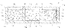
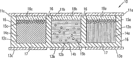
图1是电泳显示器的剖面示意图,示意了在不带电条件下的三个微型杯盒。Fig. 1 is a schematic cross-sectional view of an electrophoretic display, illustrating three microcup boxes under an uncharged condition.
图2是图1中电泳显示器的剖面示意图,但对其中两个电泳施加电压,使得颜料迁移至一侧的电极板。Figure 2 is a schematic cross-sectional view of the electrophoretic display in Figure 1, but applying a voltage to two of the electrophoretic displays so that the pigment migrates to one electrode plate.
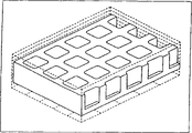
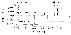
图3A-3C是典型微型杯阵列的轮廓示意图,图3A为透视图,图3B为俯视图,图3C为正视图,为了清晰将纵坐标放大。3A-3C are schematic outline diagrams of a typical microcup array. FIG. 3A is a perspective view, FIG. 3B is a top view, and FIG. 3C is a front view. The ordinate is enlarged for clarity.
图4A及4B是制备微型杯的基本方法步骤示意图,包括通过对涂布有热固性前体物的导电膜的光掩模(“顶部曝光”),用紫外光辐射进行图形光蚀刻曝光。4A and 4B are schematic diagrams of the basic process steps for making microcups, including patterned photolithographic exposure with UV radiation through a photomask ("top exposure") of a conductive film coated with a thermosetting precursor.
图5A及5B是制备微型杯的另一种处理步骤示意图,包括结合底部和顶部曝光原则的图形光蚀刻方法,这里,杯壁的固化在一个侧向是由顶部光掩模曝光,在与之垂直的侧向取向中是从底部通过不透明的基底导电膜曝光(“混合曝光”)。5A and 5B are schematic diagrams of another processing step for the preparation of microcups, including a pattern photolithography method combining bottom and top exposure principles. In the vertical lateral orientation exposure is from the bottom through the opaque base conductive film ("hybrid exposure").
图6A-6D是微型杯阵列的剖面序列图,图示了单色显示器的制成步骤。6A-6D are a sequence of cross-sectional views of microcup arrays illustrating the fabrication steps of a monochrome display.
本发明详述Detailed description of the invention
I.定义I. Definition
除非在本专利说明书中另有定义,否则在此所用的技术术语皆根据本领域技术人员通常使用并了解的惯用定义而被使用。Unless otherwise defined in this patent specification, the technical terms used herein are used according to the customary definitions commonly used and understood by those skilled in the art.
术语“微型杯”是指一种杯状凹处,其可利用上述共同未决专利申请中描述的,如微模压或图像曝光的方法制造。同样地,在整个上下文中复数形式的“微型杯”,一般是指包含多个此种微型杯共同形成或结合形成的二维结构的微型杯阵列。The term "microcup" refers to a cup-shaped recess that can be fabricated using methods such as micromolding or image exposure as described in the above co-pending patent application. Likewise, the plural form of "microcups" in the entire context generally refers to a microcup array comprising a two-dimensional structure formed jointly or combined by a plurality of such microcups.
在本专利说明书中,术语“盒”是指由一密封微型杯所形成的独立的单元。该盒以分散于溶剂或溶剂混合物中的带电荷颜料微粒填充。In this patent specification, the term "cassette" refers to a self-contained unit formed by a sealed microcup. The cartridge is filled with charged pigment particles dispersed in a solvent or solvent mixture.
当说明该微型杯或盒时,术语“有明确定义的”是指该微型杯或盒具有根据本方法的特定参数预定的明确的形状、尺寸、式样、和纵横比。The term "well-defined" when referring to the microcup or cartridge means that the microcup or cartridge has a well-defined shape, size, form, and aspect ratio predetermined according to the specific parameters of the method.
术语“纵横比”为电泳显示器中一般所知的词汇,指的是微型杯开口的深度对宽度或深度对直径的比例。The term "aspect ratio" is a commonly known term in electrophoretic displays and refers to the ratio of depth to width or depth to diameter of a microcup opening.
术语“图像曝光”指的是使用本发明所述方法之一,对辐射曝光材料或光致抗蚀剂进行辐射曝光,如紫外光曝光。藉此控制曝光材料区域以形成对应微型杯结构图案或“图像”,例如,曝光限制于对应微型杯杯壁部分的材料区域,保留微型杯底部区域不曝光。在选择性开启预定微型杯阵列部分的光致抗蚀剂的情况下,图像曝光指对应微型杯开杯区域的材料进行曝光,保留微型杯杯壁未曝光。图案或图像可以利用如透过掩模的曝光方法,或者利用可控粒子光束曝光等类似方法形成。The term "image-wise exposure" refers to exposing a radiation-exposed material or photoresist to radiation, such as ultraviolet light, using one of the methods described herein. Exposure to areas of material is thereby controlled to form a pattern or "image" corresponding to the microcup structure, eg, exposure is limited to areas of material corresponding to portions of the microcup wall, leaving areas of the bottom of the microcup unexposed. In the case of selective opening of the photoresist in predetermined portions of the microcup array, image exposure refers to exposing material corresponding to the open areas of the microcups, leaving the walls of the microcups unexposed. Patterns or images can be formed using exposure methods such as through a mask, or using controlled particle beam exposure or similar methods.
II.微型杯阵列II. Microcup Arrays
图1和图2是典型的微型杯阵列集合实施例剖面示意图,为了清晰起见已经简化,示意了由三个微型杯盒(12a,b,c)组成的一个微型杯阵列集合(10)。Figures 1 and 2 are schematic cross-sectional views of typical microcup array embodiments, which have been simplified for clarity, and illustrate a microcup array set (10) composed of three microcup boxes (12a, b, c).
如图1所示,阵列(10)的每一个盒(12)包括两个电极板(11,13),至少其中一个为透明的(11),如ITO电极,电极(11,13)位于盒(12)的两个相对面上。As shown in Figure 1, each box (12) of array (10) comprises two electrode plates (11,13), at least one of them is transparent (11), as ITO electrode, and electrode (11,13) is positioned at box (12) on two opposite faces.
微型杯盒阵列集合(10)包括多个在一个平面内被相邻放置以形成封闭在两电极层(11)和(13)之间的一个盒(12)层。图示典型的三个盒(12a),(12b),及(12c),并与各自的电极板(11a)、(11b)、(11c)(透明),以及(13a)、(13b)、(13c)(后极板)结合,大量此类盒适宜进行二维排列(在图1所示平面的右/左及里/外),以形成任选区域的二维的薄片状显示器。尽管为了清晰起见,图1示出的例子是每一个盒(12)以仅有单个盒宽度的分开的电极板(11)和(13)固定,但是类似地,几个微型杯盒也可以由一个的电极板(11)或(13)固定。The microcup box array set (10) comprises a plurality of boxes (12) layers which are adjacently placed in a plane to form a box (12) enclosed between two electrode layers (11) and (13). Figure typical three boxes (12a), (12b), and (12c), and with respective electrode plates (11a), (11b), (11c) (transparent), and (13a), (13b), (13c) (rear plate) combination, a large number of such cells are suitable for two-dimensional arrangement (right/left and inside/outside of the plane shown in Figure 1) to form a two-dimensional sheet-like display of an optional area. Although for the sake of clarity, Fig. 1 shows an example where each cartridge (12) is secured by separate electrode plates (11) and (13) having only a single cartridge width, similarly several microcup cartridges could be made of One electrode plate (11) or (13) is fixed.
该盒具有明确定义的形状和尺寸,并以分散和悬浮有带电荷颜料微粒(15)的着色介电溶剂(14)填充。每个盒(12)可以填充以相同成分的颜料和溶剂(即单色显示器),或填充以不同成分的颜料和溶剂(即彩色显示器)。图1以不同阴影线表示在每个盒(12a),(12b),及(12c)中三种不同颜色组合,溶剂分别为(14a),(14b),及(14c),颜料微粒分别为(15a),(15b),及(15c)。The box has a well-defined shape and size and is filled with a colored dielectric solvent (14) in which charged pigment particles (15) are dispersed and suspended. Each cartridge (12) can be filled with pigment and solvent of the same composition (ie monochrome displays), or with pigments and solvents of different compositions (ie color displays). Figure 1 represents three different color combinations in each box (12a), (12b) and (12c) with different hatching, the solvent is respectively (14a), (14b), and (14c), and the pigment particles are respectively (15a), (15b), and (15c).
每个微型杯盒(12)由以下部分构成:盒壁(16)作为盒的侧面(在阵列(10)的平面内),底部(17)作为盒的一个面,在本例中该面与电极(13)紧临。在每一盒的对面(紧临电极(11)),由密封覆盖层部分(18)构成。密封覆盖层部分与透明电极(11)相邻(如图1所示),密封覆盖层(18)由透明组分构成。尽管在图1所示例中,底部(17)和密封覆盖层(18)显示为不同于相邻电极(13)和(11)的分别分开的盒部分,在本发明其他的实施例中,微型杯阵列(10)可以由整体式的底部/电极结构或整体式的密封覆盖层/电极结构组成。Each microcup box (12) consists of the box walls (16) as sides of the box (in the plane of the array (10)) and the bottom (17) as a face of the box, which in this example is aligned with the Electrode (13) is next to. On the opposite side of each box (next to the electrodes (11)), a sealing cover layer section (18) is formed. The sealing covering layer part is adjacent to the transparent electrode (11) (as shown in Fig. 1), and the sealing covering layer (18) is composed of a transparent component. Although in the example shown in Figure 1, the base (17) and sealing cover (18) are shown as separate box parts from the adjacent electrodes (13) and (11), in other embodiments of the invention, the miniature The cup array (10) may consist of a unitary bottom/electrode structure or a unitary hermetic cover/electrode structure.
图2是图1中电泳显示器的剖面示意图,但对其中两个电泳盒(12a,12c)施加电压,使得颜料迁移至一侧的电极板。当于两极板(11,13)之间施加电压差时,带电荷的微粒(15)发生迁移(即向电极(11)或(13)迁移,其方向取决于微粒和电极所带电荷),因而,透过透明的导电膜(11),可看到颜料微粒(15)的颜色或溶剂(14)的颜色。二导体(11)或(13)中至少有一个是图形化的(独立的可寻址区),以允许对应每个盒或预定的盒组建立选择性的电场(即形成一个像素)。Fig. 2 is a schematic cross-sectional view of the electrophoretic display in Fig. 1, but voltage is applied to two of the electrophoretic cells (12a, 12c), so that the pigment migrates to the electrode plate on one side. When a voltage difference is applied between the two plates (11, 13), the charged particles (15) migrate (i.e. migrate to the electrode (11) or (13), the direction of which depends on the charge on the particles and electrodes), Thus, through the transparent conductive film (11), the color of the pigment particles (15) or the color of the solvent (14) can be seen. At least one of the two conductors (11) or (13) is patterned (independently addressable areas) to allow the establishment of a selective electric field (ie to form a pixel) for each cell or predetermined group of cells.
在图2所示实施例中,两个盒(12a和12c)带电,其中的颜料(15a和15c)分别迁移至各自的透明电极板(11a和11c)。剩下的盒(12b)保持中性,颜料(15b)分散于全部溶剂(14b)中。In the embodiment shown in Figure 2, two cartridges (12a and 12c) are charged and the pigments (15a and 15c) therein migrate to their respective transparent electrode plates (11a and 11c). The remaining cartridge (12b) remains neutral and the pigment (15b) is dispersed in the total solvent (14b).
图3A-3C是典型微型杯阵列局部轮廓示意图,图3A为透视图,图3B为俯视图,图3C为正视图,为了表示清楚而将纵坐标放大。对于反射型电泳显示器,每一单个的微型杯的开口面积较好为约102至约5×10⁵平方微米之间,优选为约103至约5×10⁴平方微米之间。微型杯(12)的宽度w(相邻壁面(16)间距)可在很大范围变化,可按照最终需要的显示器特性选择。微型杯的开口宽度较好为约15至约450微米之间,优选地,开口的一边至另一边为约25至约300微米之间。每一微型杯都可构成最终显示器像素的一小部分或者构成完整像素。3A-3C are partial schematic diagrams of a typical microcup array. FIG. 3A is a perspective view, FIG. 3B is a top view, and FIG. 3C is a front view. The ordinate is enlarged for clarity. For reflective electrophoretic displays, the opening area of each individual microcup is preferably between about 10 2 and about 5×10 5 square microns, preferably between about 10 3 and about 5×10 4 square microns. The width w (the distance between adjacent walls (16)) of the microcup (12) can vary in a wide range, and can be selected according to the final required display characteristics. The opening width of the microcup is preferably between about 15 and about 450 microns, preferably between about 25 and about 300 microns from one side of the opening to the other side. Each microcup can form a fraction of a final display pixel or form a complete pixel.
相对于杯宽度w的壁厚t可以在很大范围变化,可按照最终需要的显示器特性选择。微型杯壁厚通常为微型杯宽度的约0.01至1倍,优选为微型杯宽度的约0.05至约0.25倍。开口面积对总面积比较好为约0.1至约0.98,优选为约0.3至约0.95。The wall thickness t relative to the cup width w can vary widely and can be selected according to the final desired display characteristics. The microcup wall thickness is typically about 0.01 to 1 times the width of the microcup, preferably about 0.05 to about 0.25 times the width of the microcup. The ratio of open area to total area is preferably from about 0.1 to about 0.98, preferably from about 0.3 to about 0.95.
为清楚起见,对微型杯壁高h(定义为杯的深度),以放大的尺寸比例表示。对于电泳显示器,微型杯高度通常为约5至约100微米(μms),优选为约10至约50微米。对于液晶显示器,该高度通常为约1至10微米,优选为约2至5微米。For clarity, the microcup wall height h (defined as the depth of the cup) is expressed on an exaggerated scale. For electrophoretic displays, the microcup height is typically about 5 to about 100 microns (μms), preferably about 10 to about 50 microns. For liquid crystal displays, this height is generally about 1 to 10 microns, preferably about 2 to 5 microns.
为了简化和清楚,本发明在这里对微型杯阵列集合的说明中采用排列在线性二维阵列集合中的方形微型杯。但该微型杯不必需是正方形的,也可以是长方形、圆形、或是所需的一种更复杂的形状。例如,微型杯可以是六边形并采取六边形紧密排列阵列,或者三角形微型杯可以取向排列成为六边形的子阵列,该子阵列转而再排列为六边形紧密排列阵列。For simplicity and clarity, the present invention is described herein with respect to microcup array sets using square-shaped microcups arranged in a linear two-dimensional array set. But the microcup does not have to be square, it can also be rectangular, circular, or a more complex shape as desired. For example, the microcups may be hexagonal in shape and in a hexagonal close-packed array, or triangular-shaped microcups may be oriented in a hexagonal sub-array which in turn is arranged in a hexagonal close-packed array.
通常情况,微型杯可以是任意形状,且在整个显示器中其尺寸、式样、及形状可以变化。这在彩色电泳显示器中很有利。为获得最佳光学效果,可以制造不同形状和尺寸的微型杯。例如,为了制造彩色电泳显示器,填充红色分散物的微型杯可具有与绿色微型杯或蓝色微型杯不同的形状和尺寸。此外,一个像素可以由不同颜色的不同数目的微型杯组成。例如,一个像素可以由一定数量小的绿微型杯、一定数量大的红微型杯、和一定数量小的蓝微型杯组成。不必要使三种颜色微型杯具有相同的形状和数目。In general, microcups can be of any shape and can vary in size, style, and shape throughout the display. This is advantageous in color electrophoretic displays. For optimal optical results, microcups can be manufactured in different shapes and sizes. For example, to make a color electrophoretic display, a microcup filled with a red dispersion may have a different shape and size than a green or blue microcup. Furthermore, a pixel can be composed of different numbers of microcups of different colors. For example, a pixel may consist of a certain number of small green microcups, a certain number of large red microcups, and a certain number of small blue microcups. It is not necessary for the three color microcups to have the same shape and number.
微型杯的开口可以是圆形的、正方形的、长方形的、六边形的,或任意的其他形状。在维持理想的机械性能的前提下,开口之间的分隔区域要尽可能小,以获得高的色彩饱和度和对比度。因而,例如与圆形开口相比,蜂窝状开口更佳。The opening of the microcup can be circular, square, rectangular, hexagonal, or any other shape. The separation area between the openings was kept as small as possible to achieve high color saturation and contrast while maintaining ideal mechanical properties. Thus, for example, honeycomb openings are preferred over circular openings.
III.微型杯阵列的制备III. Preparation of Microcup Arrays
微型杯可以由微模压或光刻法制备。Microcups can be fabricated by micromolding or photolithography.
IIIa.微模压法制备微型杯阵列IIIa. Fabrication of Microcup Arrays by Micromolding
凸模的制备Preparation of punch
凸模可用任何适当的方法制备,例如金刚石切割工艺或用光致抗蚀剂处理后,接着蚀刻或电镀。用于凸模的主模板则可以用任何适当的方法制造,例如电镀。采用电镀法时,在一玻璃基板上喷镀一层通常为3000的籽金属薄层,例如铬镍铁合金。接着涂布一层光致抗蚀剂层,并以紫外光曝光。一掩模被置于紫外光和光致抗蚀剂层之间。该光致抗蚀剂的曝光区域变硬。然后用适当的溶剂清洗去除未曝光区域。对保留的固化光致抗蚀剂进行干燥,并再次喷镀一层籽金属薄层。主模准备就绪进行电铸成形。用于电铸成形的典型材料是镍钴合金。此外,该主模可由镍制作,如摄影光学仪器工程师学会会刊卷1663,pp.324(1992)中《薄镀层光学介质的连续制作》(“Continuous manufacturing of thin cover sheet opticalmedia”,SPIE Proc.)中所说明的,采用电铸或无电镍沉积。该模具的底板通常约50至400微米。该主模也可用其他微工程技术制作,包括电子束写入、干式蚀刻、化学蚀刻、激光写入或激光干涉,如摄影光学仪器工程师学会会刊刊登的《精密光学复制技术》(“Replication techniques for micro-optics”,SPIE Proc.)卷3099,PP.76-82(1997)中说明。此外,该模具可使用塑料、陶瓷、金属,利用光加工制作。The convex pattern can be prepared by any suitable method, such as a diamond cutting process or after treatment with photoresist followed by etching or electroplating. The master template for the punch can then be produced by any suitable method, such as electroplating. When the electroplating method is used, a thin layer of seed metal, such as Inconel, is sprayed on a glass substrate, usually 3000 Å. A layer of photoresist is then applied and exposed to ultraviolet light. A mask is placed between the UV light and the photoresist layer. The exposed areas of the photoresist harden. Unexposed areas are then removed by washing with an appropriate solvent. The remaining cured photoresist is dried and again deposited with a thin layer of seed metal. The master mold is ready for electroforming. Typical materials used for electroforming are nickel-cobalt alloys. In addition, the master mold can be made of nickel, such as "Continuous manufacturing of thin cover sheet optical media" in "Continuous manufacturing of thin cover sheet optical media", SPIE Proc. ), by electroforming or electroless nickel deposition. The base of the mold is typically about 50 to 400 microns. The master mold can also be fabricated using other micro-engineering techniques, including electron beam writing, dry etching, chemical etching, laser writing, or laser interference, as described in "Replication Techniques for Precision Optics" published by the Society of Photographic Optical Instrument Engineers. techniques for micro-optics”, SPIE Proc.) Volume 3099, PP.76-82 (1997). In addition, the mold can be made of plastic, ceramics, metal, and light processing.
这样制备的凸模通常具有大约1至500微米之间的凸起,较好为大约2至100微米之间,优选为大约4至50微米。凸模可以是带、辊、片的形式。对于连续制造而言,优选为带型模。The stamps thus prepared generally have protrusions of between about 1 and 500 microns, preferably between about 2 and 100 microns, preferably between about 4 and 50 microns. The punch can be in the form of a belt, roll or sheet. For continuous manufacturing, belt dies are preferred.
微型杯的形成Microcup formation
微型杯可以用批次工艺或是连续的辊至辊工艺制作,如于2001年2月25日提交的未决美国专利申请09/784,972所披露。该专利申请提供连续、低成本、高产出的制造技术,以制造电泳或液晶显示器中用的隔间。在涂敷紫外光固化树脂以前,如果需要,可采用脱模剂帮助脱模处理。在配送紫外光固化树脂前可以先除气,并且可以非必选地加入一种溶剂。这种溶剂(如果有的话)可以容易地蒸发。该紫外光固化树脂可采用任何适当的方式配送至凸模上,例如涂布、滴落、倾倒等。配送器可以是移动式的或固定式的。将一种导电膜覆盖于紫外光固化树脂上。合适的导电膜例子包括塑料基板上的透明导体ITO,该塑料为聚对苯二甲酸乙酯(polyethyleneterephthalate)、聚萘酸乙酯(polyethylene naphthalate)、芳族聚酰胺(polyaramid)、聚酰亚胺、聚环烯、聚砜(polysulfone)、环氧化物,及它们的组合物。如果需要的话,可以施加压力,以确保树脂和塑料之间有适当的接合,并控制微型杯底板的厚度。可以采用层压辊、真空模塑成型、加压装置、或任何其它类似的装置来施加压力。如果凸模是金属的并且不透明,则典型的塑料基板对于用来固化树脂的光化性辐射而言是透明的。反之,凸模可以是透明的,而塑料基板对于光化性辐射而言是不透明的。为了将模压特征良好地转移到转移片上,塑料基板必须对于紫外光固化树脂具有良好的粘合性。Microcups can be made using a batch process or a continuous roll-to-roll process, as disclosed in pending US patent application Serial No. 09/784,972, filed February 25,2001. This patent application provides continuous, low-cost, high-throughput manufacturing techniques to create compartments for use in electrophoretic or liquid crystal displays. Before applying the UV-curable resin, if necessary, a release agent can be used to assist in the release process. UV curable resins can be degassed prior to distribution and optionally a solvent can be added. Such solvents, if present, can be readily evaporated. The UV-curable resin can be delivered to the male mold in any suitable manner, such as coating, dripping, pouring and the like. Dispensers can be mobile or stationary. A conductive film is overlaid on the UV curable resin. Examples of suitable conductive films include transparent conductor ITO on a plastic substrate such as polyethylene terephthalate, polyethylene naphthalate, polyaramid, polyimide , polycycloolefin, polysulfone (polysulfone), epoxy, and their composition. Pressure can be applied, if desired, to ensure a proper bond between the resin and plastic and to control the thickness of the microcup base plate. Pressure may be applied using lamination rolls, vacuum molding, pressing devices, or any other similar device. While the stamp is metallic and opaque, a typical plastic substrate is transparent to the actinic radiation used to cure the resin. Conversely, the male mold can be transparent while the plastic substrate is opaque to actinic radiation. In order to transfer the molded features well to the transfer sheet, the plastic substrate must have good adhesion to the UV curable resin.
IIIb.光蚀刻法制备微型杯阵列IIIb. Fabrication of Microcup Arrays by Photolithography
在图4和5中图示了制备微型杯阵列的光蚀刻方法。The photolithography process for fabricating microcup arrays is illustrated in FIGS. 4 and 5 .
顶部曝光top exposure
如图4A和4B所示,微型杯阵列(40)可用已知方法涂布至一导电电极膜(42)上的辐射固化材料(41a),通过光掩模(46)用紫外光(或选择其他形式的辐射、电子束等)曝光,以形成与光掩模投影图形一致的壁(41b)的方法来制备。基底导电膜(42)优选以基底衬板(43)为衬底,该衬板由一种塑料材料组成。As shown in Figures 4A and 4B, the microcup array (40) can be coated with a radiation-curable material (41a) on a conductive electrode film (42) by known methods, and exposed to ultraviolet light (or selectivity) through a photomask (46). Other forms of radiation, electron beam, etc.) exposure to form the wall (41b) consistent with the photomask projected pattern. The base conductive film (42) is preferably backed by a base backing (43) which consists of a plastic material.
在图4A的掩模(46)中,深色方块(44)表示不透明区域,深色方块之间的部位表示掩模(46)的透明区域(45)。紫外光穿过透明区域(45)辐射到辐射固化材料(41a)上。优选对辐射固化材料(41a)直接曝光,即紫外光没有通过基底(43)或基底导电膜(42)(顶部曝光)。这样,基底(43)和导电膜(42)都不需要对于紫外光或所用其他辐射波长透明。In the mask (46) of FIG. 4A, the dark squares (44) represent opaque regions, and the areas between the dark squares represent transparent regions (45) of the mask (46). Ultraviolet light is radiated through the transparent region (45) onto the radiation curable material (41a). Direct exposure to the radiation curable material (41a) is preferred, ie the UV light does not pass through the substrate (43) or the substrate conductive film (42) (top exposure). Thus, neither the substrate (43) nor the conductive film (42) need be transparent to ultraviolet light or other wavelengths of radiation used.
如图4B中所示,曝光区(41b)变硬,接着用适当的溶剂或显影剂去除未曝光区域(被掩模(46)的不透明区域(44)所保护),以制作微型杯(47)。溶剂或显影剂从通常用于溶解或降低辐射固化材料粘度的材料中选择,例如甲基乙基酮(MEK)、甲苯、丙酮、异丙醇等等。也可用将掩模置于导电膜/基底衬板下的类似的方法完成微型杯的制备,在这种情况下,紫外光从底部透过掩模进行辐射,并且,基底衬板需要对辐射透明。As shown in Figure 4B, the exposed areas (41b) are hardened, and then the unexposed areas (protected by the opaque areas (44) of the mask (46)) are removed with a suitable solvent or developer to produce microcups (47 ). The solvent or developer is selected from materials commonly used to dissolve or reduce the viscosity of radiation curable materials, such as methyl ethyl ketone (MEK), toluene, acetone, isopropanol, and the like. Fabrication of microcups can also be done in a similar way by placing a mask under a conductive film/substrate backing, in this case UV light is irradiated from the bottom through the mask and the backing needs to be radiation transparent .
通过不透明导电区带曝光Exposure through opaque conductive zone
本发明中制备微型杯阵列还有另外一种可选择的方法,如图5A和5B所示的图像曝光方法。可使用不透明导电区带,将其用作从底部曝光的掩模。从顶部透过具有垂直于前述导电区带的不透明区带的第二光掩模进行附加曝光,获得耐用的微型杯杯壁。There is another optional method for preparing microcup arrays in the present invention, such as the image exposure method shown in Figures 5A and 5B. An opaque conductive zone can be used as a mask for exposure from the bottom. Additional exposure from the top through a second photomask having opaque zones perpendicular to the aforementioned conductive zones results in a durable microcup wall.
图5A图示了用顶部和底部曝光的原理,制备本发明中微型杯阵列(50)。基底导电膜(52)不透明且为区带图案。涂布于基底导电膜(52)和基底(53)上的辐射固化材料(51a),通过用作第一掩模的导电区带图形(52)从底部曝光。透过具有垂直于前述导电区带图案的第二掩模(56),第二次曝光是从顶部进行的。在区带(54)之间的间隔(55)对紫外光基本透明。在本方法中,壁材料(51b)在在一个侧向取向上是从底部向上固化,在与之垂直的侧面取向中是从顶部向下固化,共同形成一个完整的微型杯(57)。Fig. 5A illustrates the principle of top and bottom exposure to prepare the microcup array (50) of the present invention. The base conductive film (52) is opaque and has a zone pattern. The radiation curable material (51a) coated on the base conductive film (52) and the substrate (53) is exposed from the bottom through the conductive zone pattern (52) used as a first mask. A second exposure is performed from the top through a second mask (56) having a pattern of conductive zones perpendicular to the aforementioned. The spaces (55) between the zones (54) are substantially transparent to ultraviolet light. In this method, the wall material (51b) is cured from the bottom up in one lateral orientation and from the top down in the perpendicular lateral orientation, together forming a complete microcup (57).
如图5B所示,按照上文所述方法,用溶剂或显影剂去除未曝光部分,显现微型杯(57)。As shown in Figure 5B, the microcups (57) are revealed by removing the unexposed portions with a solvent or developer, as described above.
IV.本发明的密封组分和方法IV. SEALING COMPOSITIONS AND METHODS OF THE INVENTION
这种新颖的密封覆盖组分包括以下部分:This novel seal covering component consists of the following components:
(1)溶剂或者溶剂混合物,其与微型杯中的显示器流体不互溶,并且较显示器流体的比重低;以及(1) a solvent or solvent mixture that is immiscible with the display fluid in the microcup and has a lower specific gravity than the display fluid; and
(2)热塑性弹性体。(2) Thermoplastic elastomer.
含有热塑性弹性体,对微型杯有良好的相容性,并对显示器流体有良好的阻隔性的密封组分特别有用。有用的热塑性弹性体的例子包括:ABA和(AB)n型二嵌段共聚物、三嵌段共聚物、及多嵌段共聚物,其中,A为苯乙烯、α-甲基苯乙烯、乙烯、丙烯、降冰片烯(norbornene);B为丁二烯、异戊二烯、乙烯、丙烯、丁烯、二甲基硅氧烷、或者是硫化丙烯;式中A和B不可以相同。数字n≥1,优选为1-10。苯乙烯或者α-甲基苯乙烯的二嵌段或者三嵌段共聚物特别有用,例如SB(聚(苯乙烯-b-丁二烯))、SBS(聚(苯乙烯-b-丁二烯-b-苯乙烯))、SIS(聚(苯乙烯-b-异戊二烯-b-苯乙烯))、SEBS(聚(苯乙烯-b-乙烯/丁烯-b-苯乙烯))、聚(苯乙烯-b-二甲基硅氧烷-b-苯乙烯)、聚(α-甲基苯乙烯-b-异戊二烯)、聚(α-甲基苯乙烯-b-异戊二烯-b-α-甲基苯乙烯)、聚(α-甲基苯乙烯-b-硫化丙烯-b-α-甲基苯乙烯)、聚(α-甲基苯乙烯-b--二甲基硅氧烷-b-α-甲基苯乙烯)。在N.R.Legge,G.Holden和H.E.Schroeder编著的《热塑性弹性体》(Hanser出版社,1987)中可以找到制备热塑性弹性体的介绍。Kraton Polymer公司(得克萨斯州休斯顿)销售的Kraton D和G系列的苯乙烯嵌段共聚物很有用。发现结晶橡胶,如聚(乙烯-共-丙烯-共-5-亚甲基-2-降冰片烯),或者EPDM(乙烯-丙烯-二烯烃三元共聚物)橡胶,如Vistalon 6505(得克萨斯州休斯顿Exxon Mobile公司销售),以及它们的接枝共聚物也非常有用。Sealing components containing thermoplastic elastomers, good compatibility with microcups, and good barrier properties to display fluids are particularly useful. Examples of useful thermoplastic elastomers include: ABA and (AB)n-type diblock copolymers, triblock copolymers, and multiblock copolymers, wherein A is styrene, α-methylstyrene, ethylene , propylene, norbornene (norbornene); B is butadiene, isoprene, ethylene, propylene, butene, dimethylsiloxane, or propylene sulfide; where A and B cannot be the same. The number n≥1, preferably 1-10. Diblock or triblock copolymers of styrene or α-methylstyrene are particularly useful, such as SB (poly(styrene-b-butadiene)), SBS (poly(styrene-b-butadiene -b-styrene)), SIS(poly(styrene-b-isoprene-b-styrene)), SEBS(poly(styrene-b-ethylene/butylene-b-styrene)), Poly(styrene-b-dimethylsiloxane-b-styrene), poly(α-methylstyrene-b-isoprene), poly(α-methylstyrene-b-isoamyl Diene-b-α-methylstyrene), poly(α-methylstyrene-b-sulfurized propylene-b-α-methylstyrene), poly(α-methylstyrene-b--di methylsiloxane-b-alpha-methylstyrene). An introduction to the preparation of thermoplastic elastomers can be found in "Thermoplastic Elastomers" edited by N.R. Legge, G. Holden and H.E. Schroeder (Hanser Verlag, 1987). The Kraton D and G series of styrenic block copolymers sold by Kraton Polymer (Houston, Texas) are useful. Found in crystalline rubbers such as poly(ethylene-co-propylene-co-5-methylene-2-norbornene), or EPDM (ethylene-propylene-diene terpolymer) rubbers such as Vistalon 6505 (Texas Exxon Mobile, Houston), and their graft copolymers are also very useful.
不为理论局限,发明人相信:在密封涂层干燥中或者之后,热塑性弹性体硬块发生相分离,并作为软的连续相的物理交联剂。本发明的密封组分在整个密封层涂布和干燥过程中明显地强化了密封层的模数和膜完整性。具有低临界表面张力(低于40达因/厘米)和高模数或者高的肖氏A硬度(高于60)的热塑性弹性体,可能由于其对显示器流体的良好的润湿性和膜完整性,因而非常有用。Without wishing to be bound by theory, the inventors believe that during or after the seal coat dries, the hard mass of thermoplastic elastomer phase separates and acts as a physical crosslinker for the soft continuous phase. The sealant composition of the present invention significantly enhances the modulus and film integrity of the sealer throughout the sealer coating and drying process. Thermoplastic elastomers with low critical surface tension (less than 40 dynes/cm) and high modulus or high Shore A hardness (above 60), possibly due to their good wetting and film integrity to display fluids nature, so it is very useful.
将热塑性材料溶于溶剂或溶剂混合物中,该溶剂或混合物与微型杯中的显示流体不互溶,并具有低于显示流体的比重。由于对微型杯表面和电泳流体具有更好的润湿性能,低表面张力的溶剂更适于作外涂布组分。表面张力较好为低于35达因/厘米。表面张力优选为低于30达因/厘米。合适的溶剂包括烷烃(优选为C6-12的烷烃,如庚烷、辛烷、Exxon化学公司的Isopar溶剂、壬烷、癸烷及其异构体),环烷烃(优选为C6-12环烷烃,例如:环己烷、十氢化萘等等)、烷基苯(优选为单取代或二取代的C1-6的烷基苯如甲苯、二甲苯等等),烷基酯类(优选为C2-5的烷基酯如醋酸乙酯、醋酸异丁酯等等),以及C3-5的烷基醇(如异丙醇及其同类物和异构体)。烷基苯和烷烃的混合物非常有用。The thermoplastic material is dissolved in a solvent or solvent mixture that is immiscible with the display fluid in the microcup and has a lower specific gravity than the display fluid. Solvents with low surface tension are more suitable for overcoating components due to better wetting properties on the microcup surface and electrophoretic fluid. The surface tension is preferably less than 35 dynes/cm. The surface tension is preferably below 30 dynes/cm. Suitable solvents include alkanes (preferably C 6-12 alkanes such as heptane, octane, Isopar solvent from Exxon Chemical Company, nonane, decane and its isomers), cycloalkanes (preferably C 6-12 Cycloalkanes, such as cyclohexane, decahydronaphthalene, etc.), alkylbenzenes (preferably monosubstituted or disubstituted C 1-6 alkylbenzenes such as toluene, xylene, etc.), alkyl esters ( Preferred are C 2-5 alkyl esters such as ethyl acetate, isobutyl acetate, etc.), and C 3-5 alkyl alcohols (such as isopropanol and its congeners and isomers). Mixtures of alkylbenzenes and alkanes are very useful.
为了提高对微型杯密封的粘附性,并提供更灵活的涂布工艺,组分中也可以包括润湿剂(例如:3M公司的FC表面活性剂、DuPont公司的Zonyl氟化表面活性剂、氟化丙烯酸酯、氟化甲基丙烯酸酯、氟代长链醇、全氟代长链羧酸,和它们的衍生物,以及美国康奈提格州格林威治OSi公司的Silwet硅树脂表面活性剂。其他成分,在涂布过程中或之后的交联反应和聚合反应中,对于提高密封层的物理机械性质非常有用,包括交联剂(如:二叠氮化合物,例如4,4’-二叠氮基二甲苯(4,4’-diazidodiphenylmethane)和2,6-二-(4’-叠氮苯亚甲基)-4-甲基环己酮(2,6-di-(4’-azidobenzal)-4-methylcyclohexanone)),硫化剂(如2-苯噻唑基二硫化物、二硫化四甲基秋兰姆),多官能团单体或低聚体(如:己二醇、二丙烯酸酯、三甲基醇丙烷、三丙烯酸酯、二乙烯基苯、己二烯邻苯二甲酰烯(diallylnaphthalene),热引发剂(如:过氧化二月桂酰、过氧化苯甲酰),以及光引发剂(如:异丙基噻吨酮(ITX)、Ciba-Geigy公司的Irgacure 651和Irgacure 369)。To improve adhesion to microcup seals and provide a more flexible coating process, wetting agents may also be included in the composition (for example: 3M's FC Surfactant, DuPont's Zonyl Fluorinated Surfactant, Fluorinated acrylates, fluorinated methacrylates, fluorinated long-chain alcohols, perfluorinated long-chain carboxylic acids, and their derivatives, and Silwet silicone surfactants from OSi Inc., Greenwich, CT, USA Other components, in the crosslinking reaction and polymerization reaction during or after the coating process, are very useful for improving the physical and mechanical properties of the sealing layer, including crosslinking agents (such as: diazide compounds, such as 4,4'- Diazide xylene (4,4'-diazidodiphenylmethane) and 2,6-bis-(4'-azidobenzylidene)-4-methylcyclohexanone (2,6-di-(4' -azidobenzal)-4-methylcyclohexanone)), vulcanizing agent (such as 2-phenylthiazolyl disulfide, tetramethylthiuram disulfide), multifunctional monomer or oligomer (such as: hexanediol, diacrylic acid esters, trimethyl alcohol propane, triacrylates, divinylbenzene, diallylnaphthalene, thermal initiators (e.g. dilauroyl peroxide, benzoyl peroxide), and Photoinitiators (such as: isopropylthioxanthone (ITX), Irgacure 651 and Irgacure 369 from Ciba-Geigy).
通常将密封组分涂布在部分填充的微型杯中,作好外涂层的微型杯在室温下干燥。对密封后的微型杯可以用紫外光辐射或者热烘焙的方法进行后处理,以进一步提高其阻隔性能。因为在微型杯密封层的内部相形成互相渗透的网状物,使密封层对微型杯的粘接也可以通过后固化反应得到提高。Typically the sealing composition is applied to partially filled microcups and the overcoated microcups are dried at room temperature. The sealed microcup can be post-treated by ultraviolet radiation or thermal baking to further improve its barrier performance. Since an interpenetrating network is formed inside the microcup sealing layer, the adhesion of the sealing layer to the microcup can also be improved by post-curing.
V.微型杯阵列电泳显示器的制备V. Fabrication of Microcup Array Electrophoretic Display
优选的制备电泳盒的方法如图6A-6D所示。A preferred method for preparing the electrophoresis cartridge is shown in Figures 6A-6D.
如图6A所示,微型杯阵(60)可以通过上述部分III所述的任意一种方法来制备。由本文描述的方法制备的未填充的微型杯阵列通常有基底衬板(63),其上镀有底部电极(62)。微型杯的壁(61)从基板向上伸展形成开口的杯。As shown in Figure 6A, the microcup array (60) can be prepared by any of the methods described in Section III above. Unfilled microcup arrays prepared by the methods described herein typically have a base backing (63) on which a bottom electrode (62) is plated. The walls (61) of the microcup extend upwardly from the substrate to form an open cup.
如图6B所示,将微型杯填充着色介电溶剂(64)中的带电荷颜料微粒(65)的悬浮物。在所示实施例中,每个杯中的组分相同,即为单色显示器情形。为完成本发明的密封处理,微型杯优选为部分填充(以防止溢流),可以利用易挥发溶剂(如:丙酮、甲基乙基酮、异丙醇、正己烷、3M公司的FC-33全氟化溶剂)稀释电泳流体,然后其蒸发获得。当用高沸点的全氟溶剂作为显示流体的连续相时,如HT-200(新泽西Thorofare的Ausimont公司),全氟溶剂如FC-33在控制局部填充方面特别有用。As shown in Figure 6B, the microcups are filled with a suspension of charged pigment particles (65) in a colored dielectric solvent (64). In the illustrated embodiment, the components in each cup are the same, ie the case for a monochrome display. In order to complete the sealing process of the present invention, the microcup is preferably partially filled (to prevent overflow), and volatile solvents (such as: FC-33 of acetone, methyl ethyl ketone, Virahol, normal hexane, 3M company can be utilized) perfluorinated solvent) to dilute the electrophoretic fluid, which is then evaporated. Perfluorinated solvents such as FC-33 are particularly useful in controlling partial packing when high boiling perfluorinated solvents such as HT-200 (Ausimont Corporation, Thorofare, NJ) are used as the continuous phase to exhibit fluidity.
如图6C所示,填充后,用本发明的密封组分密封微型杯,以形成密封层(66)。通常在部分填充的微型杯上涂布密封组分,并显示流体上干燥。非必选地,密封后的微型杯也可以用紫外光辐射或者热烘焙进行后处理,以进一步提高其阻隔性能。As shown in Figure 6C, after filling, the microcups are sealed with the sealing composition of the present invention to form a sealing layer (66). Sealing components are typically coated on partially filled microcups and show fluid dry. Optionally, the sealed microcups can also be post-treated with ultraviolet radiation or heat baking to further improve their barrier properties.
如图6D所示,用导电膜(67)覆盖密封的电泳微型杯盒阵列(60),优选为用予施胶层(68)的导体(67),该胶层可以是压敏粘合剂,或者热熔粘合剂,或者热、湿、辐射固化粘合剂。如果顶部导电膜对辐射透明,那么可以采用诸如紫外光,透过顶部导电膜辐射对该胶层进行后固化。As shown in Figure 6D, the sealed electrophoretic microcup cartridge array (60) is covered with a conductive film (67), preferably a conductor (67) with a pre-applied adhesive layer (68), which may be a pressure sensitive adhesive , or hot melt adhesives, or heat, moisture, radiation curing adhesives. If the top conductive film is radiation transparent, the bondline can be post-cured by irradiating through the top conductive film using, for example, UV light.
VI.颜料/溶剂悬浮物或分散物组分的制备VI. Preparation of Pigment/Solvent Suspension or Dispersion Components
这里的描述是关于本发明电泳显示的各种实施例,微型杯优选填充分散在介电溶剂中的带电荷颜料微粒,(例如图6B中溶剂(64)和的颜料微粒(65))。可以用各种已知的方法制备颜料微粒分散物,例如:美国专利6,017,584号、5,914,806号、5,573,711号、5,403,518号、5,380,362号、4,680,103号、4,285,801号、4,093,534号、4,071,430号,以及3,668,106号。也可以参照电气和电子工程师协会会报-《(电子装置》(IEEE Trans.Electron Device),ED-24,827(1977),ED-24,824(1977)和J.Appl.Phys.49(9),4820(1978)。Described here in relation to various embodiments of the electrophoretic display of the present invention, the microcups are preferably filled with charged pigment particles dispersed in a dielectric solvent, (eg solvent (64) and pigment particles (65) in Figure 6B). Pigment particle dispersions can be prepared by various known methods, for example: U.S. Patent Nos. 6,017,584, 5,914,806, 5,573,711, 5,403,518, 5,380,362, 4,680,103, 4,285,801, 4,093,534, 4,071,430, and 3,668,106. Also refer to Proceedings of the Institute of Electrical and Electronics Engineers - "(IEEE Trans. Electron Device), ED-24, 827 (1977), ED-24, 824 (1977) and J.Appl.Phys.49 ( 9), 4820 (1978).
带电荷颜料微粒与其悬浮介质在视觉上存在反差。该介质是一种介电溶剂,优选具有低粘滞性,介电常数在2到30之间,为具备高微粒迁移速率,优选介电常数为约2到15。适当的介电溶剂的例子包括如十氢化萘(DECALIN)、5-亚乙基-2-降冰片烯(5-ethylidene-2-norbornene)、脂肪油、蜡下油(paraffin oil)等碳氢化合物;如甲苯、二甲苯、苯基二甲苯乙烷、十二烷基苯和烷基萘等芳香族碳氢化合物;如二氯三氟甲苯(dichlorobenzotrifluoride)、3,4,5-三氟化三氯甲苯、氯五氟基苯(chloropentafluoro-benzene)、二氯壬烷、五氯苯等卤化溶剂;如来自明尼苏达州St.Paul的3M公司的FC-43、FC-70和FC-5060的全氟溶剂;低分子量的含卤素的聚合物,如自奥勒岗州Portland的TCI America的聚全氟丙烯醚(poly(perfluoropropylene oxide));聚氯三氟乙烯,如新泽西州River Edge的Halocarbon Product公司的卤烃油;全氟聚烷基醚,如自新泽西州Thorofare的Ausimont公司的Galden、HT-200、Flurolink或是来自特拉华州DuPont的Krytox油和脂K-Fluid系列。在一个优选具体实施例中,使用聚氯三氟乙烯作为介电溶剂。在另一优选的实施例中,使用聚全氟丙烯醚(poly(perfluoropropylene oxide))作为介电溶剂。There is a visual contrast between charged pigment particles and their suspending medium. The medium is a dielectric solvent, preferably of low viscosity, with a dielectric constant between 2 and 30, preferably about 2 to 15 for high particle transport rates. Examples of suitable dielectric solvents include hydrocarbons such as DECALIN, 5-ethylidene-2-norbornene, fatty oils, paraffin oil, etc. Compounds; aromatic hydrocarbons such as toluene, xylene, phenylxyleneethane, dodecylbenzene, and alkylnaphthalene; such as dichlorobenzotrifluoride, 3,4,5-trifluorinated Halogenated solvents such as trichlorotoluene, chloropentafluoro-benzene, dichlorononane, and pentachlorobenzene; such as FC-43, FC-70, and FC-5060 from 3M Company, St. Paul, Minnesota Perfluorinated solvents; low molecular weight halogen-containing polymers such as poly(perfluoropropylene oxide) from TCI America, Portland, Oregon; polychlorotrifluoroethylene, such as Halocarbon from River Edge, New Jersey Halocarbon oils from Product Corporation; perfluoropolyalkyl ethers such as Galden, HT-200, Flurolink from Ausimont, Thorofare, NJ or Krytox oils and fats K-Fluid series from DuPont, Delaware. In a preferred embodiment polychlorotrifluoroethylene is used as the dielectric solvent. In another preferred embodiment, poly(perfluoropropylene oxide) is used as the dielectric solvent.
从染料或颜料中可以形成一种非迁移流体着色剂。非离子偶氮物和蒽醌染料非常有用。有用染料的例子非限定性地包括:亚利桑那州Pylam Producrts公司的油溶红EGN(Oil Red EGN)、苏丹红、苏丹蓝、油溶蓝(Oil Blue)、Macrolex蓝、溶剂蓝35,亚利桑那州Pylam Products公司的Pylam Spirit黑和Fast Spirit黑;Aldrich公司的Sudan黑B(Sudan Black B);BASF公司的Thermoplastic BlackX-70;Aldrich公司的蒽醌蓝、蒽醌黄114、蒽醌红111和135、蒽醌绿28。在使用全氟化溶剂时,氟化染料非常有用。在使用颜料时,用来使介质产生颜色的非迁移性颜料也可以分散在介电介质中。这些颜料微粒以不带电荷的为好。如果用来使介质产生颜色的非迁移性颜料带电荷,则其最好带有与带电的、迁移性颜料颗粒相反的电荷。如果两种颜料颗粒带有相同性质的电荷,那么它们应该具有不同的电荷密度或电泳移动速率。不论在何种情况下,用来在介质中产生非迁移性流体着色剂的染料或颜料,都必须化学稳定,并且要与悬浮液中的其它成分相容。A non-migrating fluid colorant can be formed from a dye or pigment. Nonionic azo and anthraquinone dyes are very useful. Examples of useful dyes include, but are not limited to: Oil Red EGN, Sudan Red, Sudan Blue, Oil Blue, Macrolex Blue, Solvent Blue 35 from Pylam Products, Arizona, Pylam, Arizona Pylam Spirit Black and Fast Spirit Black from Products Company; Sudan Black B (Sudan Black B) from Aldrich Company; Thermoplastic BlackX-70 from BASF Company; Anthraquinone Blue, Anthraquinone Yellow 114, Anthraquinone Red 111 and 135 from Aldrich Company Anthraquinone Green 28. Fluorinated dyes are useful when using perfluorinated solvents. When pigments are used, non-migrating pigments used to impart color to the medium may also be dispersed in the dielectric medium. These pigment particles are preferably uncharged. If the non-migrating pigment used to impart color to the medium is charged, it preferably has the opposite charge to the charged, migrating pigment particles. If two pigment particles are charged with the same nature, they should have different charge densities or electrophoretic mobility rates. In any case, the dye or pigment used to produce the non-migrating fluid colorant in the medium must be chemically stable and compatible with the other ingredients in the suspension.
该带电荷颜料微粒可为有机或无机颜料,如自Sun化学制品公司的TiO2、酞菁蓝(phthalocyanine blue)、酞菁绿(phthalocyaninegreen)、二芳基黄(diarylide yellow)、二芳基AAOT黄(diarylideAAOT Yellow)、喹吖啶酮(quinacridone)、偶氮(azo)、若丹明(rhodamine)、苝系颜料(perylene pigment series);自Kanto化学制品公司的汉撒黄G(Hansa yellow G)颗粒,以及Fisher公司的碳灯黑(Carbon Lampblack)。优选的是亚微粒子尺寸。该微粒应具有可接受的光学特性,不应被介电溶剂膨胀或软化,并且应该是化学稳定的。在正常的工作条件下,所产生的悬浮物亦必须稳定且能抗沉淀、乳化或凝结。The charged pigment particles can be organic or inorganic pigments such as TiO2 , phthalocyanine blue, phthalocyanine green, diarylide yellow, diaryl AAOT from Sun Chemicals DiarylideAAOT Yellow, quinacridone, azo, rhodamine, perylene pigment series; Hansa yellow G from Kanto Chemicals ) particles, and Fisher's carbon lamp black (Carbon Lampblack). Submicron particle sizes are preferred. The microparticles should have acceptable optical properties, should not be swollen or softened by dielectric solvents, and should be chemically stable. Under normal working conditions, the resulting suspension must also be stable and resistant to sedimentation, emulsification or coagulation.
该迁移性颜料微粒可具有自然电荷,或可使用电荷控制剂直接使之带电,或可在悬浮于介电溶剂时获得电荷。适当的电荷控制剂是本领域熟知的;其可为聚合或非聚合性质,并且可为离子的或非离子的,包括自Chevron化学制品公司的离子表面活性剂,如气溶胶邻联甲苯胺(Aerosol OT)、十二烷基苯磺酸钠(dodecylbenzenesulfonate)、OLOA 1200;金属皂,如碱式石油磺酸钙(basic calcium petroleum sulphonate)、碱式水杨酸烷基钙(basiccalcium alkyl salicylate)、水杨酸烷基锌(zinc alkyl salicylate)、烷基二苯醚二磺酸盐(alkyl diphenyloxide sulphonate)(是Dow化学制品公司的Dowfax表面活性剂),聚丁烯丁二酰亚胺(polybutenesuccinimide)、顺丁烯二酸酐共聚物(maleic anhydride copolymers)、乙烯基吡咯烷酮共聚物(vinylpyrrolidone copolymer)(如来自International Specialty Products的Ganex)、(甲基)丙烯酸共聚物((meth)acrylic acid copolymers)、N,N-二甲基胺基乙基(甲基)丙烯酸乙酯共聚物[N,N-dimethylaminoethyl](meth)acrylatecopolymers]。氟化表面活性剂在全氟化碳溶剂中作为溶剂电荷控制剂特别有用。这些包括FC氟化表面活性剂,如3M公司的FC-170C、FC-171、FC-176、FC430、FC431和FC-740;以及Zonyl氟化表面活性剂,如Dupont公司的FSA、FSE、FSN、FSN-100、FSO、FSO-100、FSD和UR。The migrating pigment particles may have a natural charge, or may be charged directly using a charge control agent, or may acquire a charge when suspended in a dielectric solvent. Suitable charge control agents are well known in the art; they may be polymeric or non-polymeric in nature, and may be ionic or non-ionic, including ionic surfactants from Chevron Chemical Company, such as aerosol o-toluidine ( Aerosol OT), dodecylbenzenesulfonate, OLOA 1200; metal soaps, such as basic calcium petroleum sulphonate, basiccalcium alkyl salicylate, zinc alkyl salicylate, alkyl diphenyloxide sulphonate (Dowfax surfactant from Dow Chemical Company), polybutene succinimide , maleic anhydride copolymers, vinylpyrrolidone copolymers (such as Ganex from International Specialty Products), (meth)acrylic acid copolymers, N , N-dimethylaminoethyl (meth) ethyl acrylate copolymer [N, N-dimethylaminoethyl] (meth) acrylatecopolymers]. Fluorinated surfactants are particularly useful as solvent charge control agents in perfluorocarbon solvents. These include FC fluorinated surfactants such as 3M's FC-170C, FC-171, FC-176, FC430, FC431, and FC-740; and Zonyl fluorinated surfactants such as Dupont's FSA, FSE, FSN , FSN-100, FSO, FSO-100, FSD and UR.
可通过任何熟知的方法制备适当的带电颜料分散体,包括研磨、碾磨、球磨、气流磨(microfluidizing)以及超声波技术。例如,将细粉末形式的颜料微粒加入悬浮溶剂,所获混合物被球磨数小时,将高度团聚的干颜料粉分散成最初的微粒。虽然不是最理想的,但是在该球磨过程,可对该悬浮物添加用于产生非迁移性流体着色剂的染料或颜料。Suitable charged pigment dispersions can be prepared by any well known method, including grinding, milling, ball milling, microfluidizing and ultrasonic techniques. For example, pigment particles in fine powder form are added to a suspending solvent, and the resulting mixture is ball milled for several hours to disperse the highly agglomerated dry pigment powder into primary particles. Although not optimal, during the ball milling process, dyes or pigments for producing non-migrating fluid colorants can be added to the suspension.
可通过使用适当的聚合物将该微粒微囊化,以消除颜料微粒的沉淀或乳化,使其比重与介电溶剂的比重相适应。可用化学或物理方法完成颜料微粒的微囊化。典型的微囊化工艺包括界面聚合、原位聚合、相分离、凝聚、静电涂布、喷雾干燥、流化床涂布、以及溶剂蒸发。The particles can be microencapsulated by using suitable polymers to eliminate sedimentation or emulsification of the pigment particles, adapting their specific gravity to that of the dielectric solvent. Microencapsulation of pigment particles can be accomplished chemically or physically. Typical microencapsulation processes include interfacial polymerization, in situ polymerization, phase separation, coacervation, electrostatic coating, spray drying, fluidized bed coating, and solvent evaporation.
就黑/白的电泳显示器而言,该悬浮物包含分散于黑色溶剂中的带电荷的白色二氧化钛(TiO2)微粒,或分散于一种介电溶剂中的带电荷黑色微粒。黑色染料或染料混合物可被用于产生溶剂的黑色,如Pylam Products公司(亚利桑那州)的Pylam Spirit黑和FastSpirit黑,Aldrich公司的苏丹黑B,BASF公司的Thermoplastic BlackX-70,或一种不可溶的黑色颜料如碳黑。对于其它有色悬浮物来说,有多种可能性。对于减色系统而言,带电荷的二氧化钛(TiO2)微粒可悬浮于蓝绿色、黄色或品红色的介电溶剂中。该蓝绿色、黄色或品红色可使用染料或颜料产生。对于加色系统而言,带电荷的二氧化钛微粒可悬浮于红色、绿色、或蓝色的介电溶剂中,其中该红色、绿色、或蓝色亦可使用染料或颜料产生。大多数的应用最好采用这种红色、绿色、或蓝色系统。For black/white electrophoretic displays, the suspension comprises charged white titanium dioxide ( TiO2 ) particles dispersed in a black solvent, or charged black particles dispersed in a dielectric solvent. Black dyes or dye mixtures can be used to produce solvent blacks such as Pylam Spirit Black and FastSpirit Black from Pylam Products (Arizona), Sudan Black B from Aldrich, Thermoplastic Black X-70 from BASF, or an insoluble Black pigments such as carbon black. For other colored suspensions there are various possibilities. For subtractive systems, charged titanium dioxide ( TiO2 ) particles can be suspended in a cyan, yellow or magenta dielectric solvent. The cyan, yellow or magenta colors can be produced using dyes or pigments. For color-additive systems, charged titanium dioxide particles can be suspended in a red, green, or blue dielectric solvent, which can also be produced using dyes or pigments. Most applications are best served with this red, green, or blue system.
实施例Example
实施例1微型杯配方Embodiment 1 microcup formula
占重量35份的Ebercryl600(UCB),40份SR-399(Startomer),10份Ebecryl 4827(UCB),7份Ebecryl 1360(UCB),8份HDDA(UCB),以及0.05份Irgacure369(Ciba Specialty化学制品公司),0.01份异丙醇噻吨酮(isopropyl thioxanthone)(Aldrich公司),均匀混合,用于微模压制备。35 parts by weight of Ebercryl® 600 (UCB), 40 parts of SR-399 (Startomer®), 10 parts of Ebecryl 4827 (UCB), 7 parts of Ebecryl 1360 (UCB), 8 parts of HDDA (UCB), and 0.05 parts of Irgacure® 369 (Ciba Specialty Chemicals Company), 0.01 part of isopropyl thioxanthone (Aldrich Company), uniformly mixed, for micromolding preparation.
实施例2微型杯阵列的制备The preparation of embodiment 2 microcup array
由5份Ebecryl 830,2.6份SR-399(Sartomer公司),1.8份Ebecry1701,1份PMMA(分子量350,000,Aldrich公司),0.5份Irgacure500,40份甲基乙酮(MEK)组成的初始溶液,用一#3Myrad棒将其涂布在2密耳(1/1000英寸)的60欧姆/□(方块电阻单位ohm/sq)的ITO/PET膜(蒙大拿州Sheldahl公司),干燥,使用Zeta7410(5瓦/厘米2,自Loctite公司)曝光装置在空气中进行紫外光固化15分钟。按照实施例1方法制备的微型杯配方组分,涂布在经过处理的ITO/PET膜上,目标厚度约50微米,用Ni-Co阳模进行模压,其上有60(长)×60(宽)微米、高度为25-50微米的重复突起方块,间隔为10微米宽。从PET侧进行紫外固化20秒,用2”剥离棒以4-5英尺/分钟的速度脱模。用具有对应突起高度的阳模制备出了深度为25-50微米的明确定义的微型杯。同样的步骤可以制备不同尺寸的各种微型杯阵列,例如70(长)×70(宽)×35(深)×10(间隔),100(长)×100(宽)×35(深)×10(间隔),100(长)×100(宽)×30(深)×10(间隔)微米。By 5 parts of Ebecryl 830, 2.6 parts of SR-399 (Sartomer Company), 1.8 parts of Ebecry1701, 1 part of PMMA (molecular weight 350,000, Aldrich Company), 0.5 parts of Irgacure500, 40 parts of methyl ethyl ketone (MEK) A #3 Myrad rod was coated on a 2 mil (1/1000 inch) 60 ohm/□ (sheet resistance unit ohm/sq) ITO/PET film (Sheldahl, Montana), dried, using a Zeta7410 ( 5 W/cm 2 , from Loctite Company) exposure device for UV curing in air for 15 minutes. The microcup formula component prepared according to the method of Example 1 is coated on the treated ITO/PET film with a target thickness of about 50 microns, molded with a Ni-Co male mold, and there are 60 (long) × 60 ( Width) microns, repeating raised squares of 25-50 microns in height, spaced 10 microns wide. UV curing was performed for 20 seconds from the PET side and demolded at 4-5 ft/min with a 2" peel bar. Well-defined microcups with a depth of 25-50 microns were produced using male molds with corresponding protrusion heights. The same steps can prepare various microcup arrays of different sizes, such as 70 (length) × 70 (width) × 35 (depth) × 10 (interval), 100 (length) × 100 (width) × 35 (depth) × 10 (interval), 100 (length) × 100 (width) × 30 (depth) × 10 (interval) microns.
实施例3颜料分散物Embodiment 3 pigment dispersion
用均质器将6.42克Ti Pure R706在溶液中分散,该溶液含有Ausimont公司的Fluorolink D 1.94克、Ausimont公司的Fluorolink70040.22克、3M公司的氟化铜酞化青染料0.37克、Ausimont公司的全氟代溶剂HT-20052.54克。6.42 grams of Ti Pure R706 were dispersed in the solution with a homogenizer, and the solution contained 1.94 grams of Fluorolink D of Ausimont Company, 0.22 grams of Fluorolink70040.22 grams of Ausimont Company, 0.37 grams of copper fluoride phthalocyanine dye of 3M Company, and 0.37 grams of Ausimont Company’s Fluorolink D Perfluorinated solvent HT-2005 2.54 grams.
实施例4颜料分散物Embodiment 4 pigment dispersion
与实施例3相同,所不同的是用新泽西Highstown的Elimentis公司和Du Pont公司的外包聚合物的TiO2颗粒PC-9003和Krytox,分别被取代Ti Pure R706和Fluorolink。Same as Example 3, except that TiO 2 particles PC-9003 and Krytox of Elimentis Company and Du Pont Company of Highstown, New Jersey are used to replace Ti Pure R706 and Fluorolink respectively.
实施例5微型杯密封Embodiment 5 Microcup sealing
用3M公司的挥发性全氟化共溶剂FC-33,将按照实施例3方法制备的电泳流体稀释,涂布在按照实施例2制备的35微米深的微型杯阵上。挥发性溶剂挥发,得到部分填充的微型杯阵。将溶在庚烷中的7.5%的聚异戊二烯(97%顺式,Aldrich公司),用通用的3密耳开口的刮刀式涂布器涂在部分填充的杯上。经过涂布的微型杯在室温下干燥。在微型杯阵列上形成了一无缝的约为7-8微米厚,具有合适粘度和合适均匀度的密封层。在显微镜下观察,看不到被封闭的空气泡。再用一个预涂有胶层的ITO/PET导体覆在密封的微型杯上。电泳盒有良好的抗弯曲能力,表现出令人满意的转换性能。在66℃的炉中陈化5天,无可观察到的重量损失。The electrophoretic fluid prepared according to the method in Example 3 was diluted with 3M's volatile perfluorinated co-solvent FC-33, and coated on the microcup array with a depth of 35 μm prepared in Example 2. The volatile solvent evaporates to obtain a partially filled array of microcups. 7.5% polyisoprene (97% cis, Aldrich) dissolved in heptane was applied to the partially filled cup with a conventional 3 mil opening knife applicator. The coated microcups were dried at room temperature. A seamless sealing layer about 7-8 microns thick with suitable viscosity and suitable uniformity is formed on the microcup array. Observed under a microscope, no closed air bubbles can be seen. A pre-coated ITO/PET conductor is used to cover the sealed microcup. The electrophoretic box has good resistance to bending and exhibits satisfactory switching performance. Aged in an oven at 66°C for 5 days with no observable weight loss.
实施例6微型杯密封Embodiment 6 Microcup sealing
与实施例5相同,不同之处是聚异戊二烯层减小到4微米,用2密耳开口的刮刀式涂布器涂布。在光学显微镜下,可以清晰地看到针孔和密封层开裂。Same as Example 5 except that the polyisoprene layer was reduced to 4 microns and applied with a knife coater with a 2 mil opening. Under an optical microscope, pinholes and cracking of the sealing layer can be clearly seen.
实施例7-14微型杯密封Examples 7-14 Microcup sealing
与实施例5相同,不同之处是用聚苯乙烯、聚乙烯醇缩丁醛(Butvar 72,蒙大拿州St.Louis的Solutia公司)、热塑性弹性体如SIS(Kraton D1107,15%苯乙烯)、SBS(Kraton D1101,31%苯乙烯)、SEBS(Kraton G1650和FG1901,30%苯乙烯)、和EPDM(Vistalon 6505,57%乙烯)取代密封层。结果列在表1中。如表1所示,即使在宽开口的微型杯上,使用该热塑性弹性体也能获得更薄而且质量更好的密封。Same as Example 5 except that polystyrene, polyvinyl butyral (Butvar 72, Solutia, St. Louis, Montana), thermoplastic elastomers such as SIS (Kraton D1107, 15% styrene ), SBS (Kraton D1101, 31% styrene), SEBS (Kraton G1650 and FG1901, 30% styrene), and EPDM (
表1微型杯的密封Table 1 Sealing of Microcups
虽然本发明已经参考其特定的具体实施例而加以描述,但是对于本领域的技术人员来说,可以容易地对上述实施方案进行多种修改和改进,或应用于其它领域。可以做多种的改变,以及有多种的等效物可以取代。此外,可以做许多修改来适合特殊的情况、材料、组分、方法、一个方法步骤或多个步骤,而不偏离本发明的目的、精神和范围。所有这些改动均在本发明专利申请权利要求范围内。Although the present invention has been described with reference to certain specific examples thereof, it will be readily apparent to those skilled in the art that various modifications and improvements can be made to the above-described embodiments, or applications in other fields. Various changes may be made, and various equivalents may be substituted. In addition, many modifications may be made to adapt a particular situation, material, composition, method, method step or steps without departing from the purpose, spirit and scope of the invention. All these modifications are within the scope of claims of the patent application for the present invention.
例如,应该注意到本发明用来制备微型杯阵列的方法也可以用来制备液晶显示器件。相似的,本发明中微型杯选择性填充和ITO层叠的方法也可以用于制备液晶显示器件。For example, it should be noted that the method of the present invention for the preparation of microcup arrays can also be used for the preparation of liquid crystal display devices. Similarly, the methods of selective filling of microcups and lamination of ITO in the present invention can also be used to prepare liquid crystal display devices.
因而,本发明的保护范围由权利要求所限定。Accordingly, the protection scope of the present invention is defined by the appended claims.
组件符号说明Description of component symbols
10 微型杯阵列集合10 microcup array set
11 电极板11 electrode plate
12 微型杯盒12 micro cup box
13 电极板13 electrode plate
14 着色介电溶剂14 Colored dielectric solvent
15 带电荷颜料微粒15 charged pigment particles
16 盒壁16 box wall
17 盒底部17 box bottom
18 密封覆盖层18 seal cover
40 微型杯阵列40 microcup array
41a 辐射固化材料41a Radiation-cured materials
41b 与光掩模投影图形一致的壁41b Wall consistent with photomask projection pattern
42 导电电极膜42 Conductive electrode film
43 基底衬板43 base liner
44 深色方块44 dark squares
45 透明区域45 transparent area
46 掩模46 mask
47 微型杯47 micro cups
50 微型杯阵列50 microcup array
51a 辐射固化材料51a Radiation-curing materials
51b 壁材料51b Wall material
52 基底导电膜52 base conductive film
53 基底53 base
54 区带54 zone
55 间隔55 intervals
56 第二掩模56 second mask
57 微型杯57 micro cups
60 微型杯阵60 micro cups
61 微型杯的壁61 Wall of the microcup
62 底部电极62 bottom electrode
63 基底衬板63 base liner
64 着色介电溶剂64 Colored dielectric solvent
65 带电荷颜料微粒65 charged pigment particles
66 密封层66 sealing layer
67 导电膜67 Conductive film
68 予施胶层68 pre-sizing layer
w 微型杯宽度w Micro Cup Width
t 微型杯壁厚t micro cup wall thickness
h 微型杯壁高h Micro cup wall height
Claims (37)
Applications Claiming Priority (2)
| Application Number | Priority Date | Filing Date | Title |
|---|---|---|---|
| US09/874,391 US20020188053A1 (en) | 2001-06-04 | 2001-06-04 | Composition and process for the sealing of microcups in roll-to-roll display manufacturing |
| US09/874,391 | 2001-06-04 |
Publications (2)
| Publication Number | Publication Date |
|---|---|
| CN1389534A CN1389534A (en) | 2003-01-08 |
| CN1237140C true CN1237140C (en) | 2006-01-18 |
Family
ID=25363637
Family Applications (1)
| Application Number | Title | Priority Date | Filing Date |
|---|---|---|---|
| CNB011364483A Expired - Lifetime CN1237140C (en) | 2001-06-04 | 2001-10-17 | Composition and method for sealing microcups in roll-to-roll display manufacturing |
Country Status (9)
| Country | Link |
|---|---|
| US (3) | US20020188053A1 (en) |
| EP (1) | EP1401953A1 (en) |
| JP (1) | JP4322663B2 (en) |
| KR (1) | KR100859305B1 (en) |
| CN (1) | CN1237140C (en) |
| CA (1) | CA2448440A1 (en) |
| MX (1) | MXPA03011144A (en) |
| TW (1) | TWI301211B (en) |
| WO (1) | WO2002098977A1 (en) |
Cited By (1)
| Publication number | Priority date | Publication date | Assignee | Title |
|---|---|---|---|---|
| CN100514136C (en) * | 2006-02-08 | 2009-07-15 | 财团法人工业技术研究院 | Method for manufacturing display panel |
Families Citing this family (277)
| Publication number | Priority date | Publication date | Assignee | Title |
|---|---|---|---|---|
| US6930818B1 (en) | 2000-03-03 | 2005-08-16 | Sipix Imaging, Inc. | Electrophoretic display and novel process for its manufacture |
| US6933098B2 (en) * | 2000-01-11 | 2005-08-23 | Sipix Imaging Inc. | Process for roll-to-roll manufacture of a display by synchronized photolithographic exposure on a substrate web |
| US20070237962A1 (en) | 2000-03-03 | 2007-10-11 | Rong-Chang Liang | Semi-finished display panels |
| US7408696B2 (en) | 2000-03-03 | 2008-08-05 | Sipix Imaging, Inc. | Three-dimensional electrophoretic displays |
| US7557981B2 (en) | 2000-03-03 | 2009-07-07 | Sipix Imaging, Inc. | Electrophoretic display and process for its manufacture |
| US6865012B2 (en) | 2000-03-03 | 2005-03-08 | Sipix Imaging, Inc. | Electrophoretic display and novel process for its manufacture |
| US7715088B2 (en) | 2000-03-03 | 2010-05-11 | Sipix Imaging, Inc. | Electrophoretic display |
| US6833943B2 (en) | 2000-03-03 | 2004-12-21 | Sipix Imaging, Inc. | Electrophoretic display and novel process for its manufacture |
| US7233429B2 (en) | 2000-03-03 | 2007-06-19 | Sipix Imaging, Inc. | Electrophoretic display |
| US6885495B2 (en) | 2000-03-03 | 2005-04-26 | Sipix Imaging Inc. | Electrophoretic display with in-plane switching |
| US7158282B2 (en) | 2000-03-03 | 2007-01-02 | Sipix Imaging, Inc. | Electrophoretic display and novel process for its manufacture |
| US6831770B2 (en) | 2000-03-03 | 2004-12-14 | Sipix Imaging, Inc. | Electrophoretic display and novel process for its manufacture |
| US6788449B2 (en) * | 2000-03-03 | 2004-09-07 | Sipix Imaging, Inc. | Electrophoretic display and novel process for its manufacture |
| US6947202B2 (en) * | 2000-03-03 | 2005-09-20 | Sipix Imaging, Inc. | Electrophoretic display with sub relief structure for high contrast ratio and improved shear and/or compression resistance |
| US7052571B2 (en) | 2000-03-03 | 2006-05-30 | Sipix Imaging, Inc. | Electrophoretic display and process for its manufacture |
| US6795138B2 (en) * | 2001-01-11 | 2004-09-21 | Sipix Imaging, Inc. | Transmissive or reflective liquid crystal display and novel process for its manufacture |
| US8282762B2 (en) | 2001-01-11 | 2012-10-09 | Sipix Imaging, Inc. | Transmissive or reflective liquid crystal display and process for its manufacture |
| TW556044B (en) * | 2001-02-15 | 2003-10-01 | Sipix Imaging Inc | Process for roll-to-roll manufacture of a display by synchronized photolithographic exposure on a substrate web |
| US8361356B2 (en) * | 2001-06-04 | 2013-01-29 | Sipix Imaging, Inc. | Composition and process for the sealing of microcups in roll-to-roll display manufacturing |
| US7244470B2 (en) * | 2001-07-10 | 2007-07-17 | Cantega Technologies Inc. | Protection of electrical power systems |
| TW527529B (en) | 2001-07-27 | 2003-04-11 | Sipix Imaging Inc | An improved electrophoretic display with color filters |
| TW550529B (en) * | 2001-08-17 | 2003-09-01 | Sipix Imaging Inc | An improved electrophoretic display with dual-mode switching |
| US7038670B2 (en) * | 2002-08-16 | 2006-05-02 | Sipix Imaging, Inc. | Electrophoretic display with dual mode switching |
| US7492505B2 (en) * | 2001-08-17 | 2009-02-17 | Sipix Imaging, Inc. | Electrophoretic display with dual mode switching |
| TW539928B (en) | 2001-08-20 | 2003-07-01 | Sipix Imaging Inc | An improved transflective electrophoretic display |
| TWI308231B (en) * | 2001-08-28 | 2009-04-01 | Sipix Imaging Inc | Electrophoretic display |
| JP2004004173A (en) * | 2002-05-30 | 2004-01-08 | Canon Inc | Dispersion for electrophoretic display and electrophoretic display |
| US7271947B2 (en) | 2002-08-16 | 2007-09-18 | Sipix Imaging, Inc. | Electrophoretic display with dual-mode switching |
| US7038656B2 (en) * | 2002-08-16 | 2006-05-02 | Sipix Imaging, Inc. | Electrophoretic display with dual-mode switching |
| US7166182B2 (en) * | 2002-09-04 | 2007-01-23 | Sipix Imaging, Inc. | Adhesive and sealing layers for electrophoretic displays |
| TW575646B (en) * | 2002-09-04 | 2004-02-11 | Sipix Imaging Inc | Novel adhesive and sealing layers for electrophoretic displays |
| TWI300157B (en) * | 2002-09-10 | 2008-08-21 | Sipix Imaging Inc | Electrochromic or electrodeposition display and process for their preparation |
| US7616374B2 (en) * | 2002-09-23 | 2009-11-10 | Sipix Imaging, Inc. | Electrophoretic displays with improved high temperature performance |
| TWI327251B (en) * | 2002-09-23 | 2010-07-11 | Sipix Imaging Inc | Electrophoretic displays with improved high temperature performance |
| TWI229230B (en) * | 2002-10-31 | 2005-03-11 | Sipix Imaging Inc | An improved electrophoretic display and novel process for its manufacture |
| TWI297089B (en) | 2002-11-25 | 2008-05-21 | Sipix Imaging Inc | A composition for the preparation of microcups used in a liquid crystal display, a liquid crystal display comprising two or more layers of microcup array and process for its manufacture |
| US8023071B2 (en) | 2002-11-25 | 2011-09-20 | Sipix Imaging, Inc. | Transmissive or reflective liquid crystal display |
| US9346987B2 (en) * | 2003-01-24 | 2016-05-24 | E Ink California, Llc | Adhesive and sealing layers for electrophoretic displays |
| US7572491B2 (en) * | 2003-01-24 | 2009-08-11 | Sipix Imaging, Inc. | Adhesive and sealing layers for electrophoretic displays |
| US7717764B2 (en) * | 2003-09-12 | 2010-05-18 | Bridgestone Corporation | Method of manufacturing image display panel and image display panel |
| US7177066B2 (en) * | 2003-10-24 | 2007-02-13 | Sipix Imaging, Inc. | Electrophoretic display driving scheme |
| GB0327215D0 (en) * | 2003-11-22 | 2003-12-24 | Koninkl Philips Electronics Nv | Active matrix display device and method of producing the same |
| US7279064B2 (en) * | 2003-12-18 | 2007-10-09 | Palo Alto Research Center, Incorporated | Method of sealing an array of cell microstructures using microencapsulated adhesive |
| US8535041B2 (en) * | 2006-07-28 | 2013-09-17 | Microcontinuum, Inc. | Addressable flexible patterns |
| US9307648B2 (en) | 2004-01-21 | 2016-04-05 | Microcontinuum, Inc. | Roll-to-roll patterning of transparent and metallic layers |
| US20060033676A1 (en) * | 2004-08-10 | 2006-02-16 | Kenneth Faase | Display device |
| US8643595B2 (en) * | 2004-10-25 | 2014-02-04 | Sipix Imaging, Inc. | Electrophoretic display driving approaches |
| US7042614B1 (en) | 2004-11-17 | 2006-05-09 | Hewlett-Packard Development Company, L.P. | Spatial light modulator |
| US7463409B2 (en) * | 2004-12-20 | 2008-12-09 | Palo Alto Research Center Incorporated | Flexible electrophoretic-type display |
| GB0526230D0 (en) * | 2005-12-22 | 2006-02-01 | Eastman Kodak Co | Display devices |
| WO2007100849A2 (en) | 2006-02-27 | 2007-09-07 | Microcontinuum, Inc. | Formation of pattern replicating tools |
| US8111368B2 (en) * | 2006-02-28 | 2012-02-07 | Hewlett-Packard Development Company, L.P. | Liquid crystal display |
| US8029558B2 (en) * | 2006-07-07 | 2011-10-04 | Abbott Cardiovascular Systems, Inc. | Stent and catheter assembly and method for treating bifurcations |
| US8830561B2 (en) | 2006-07-18 | 2014-09-09 | E Ink California, Llc | Electrophoretic display |
| US20150005720A1 (en) | 2006-07-18 | 2015-01-01 | E Ink California, Llc | Electrophoretic display |
| TWI491953B (en) * | 2006-07-18 | 2015-07-11 | 希畢克斯幻像有限公司 | Electrophoretic display |
| DE602007011639D1 (en) * | 2006-08-21 | 2011-02-10 | Koninkl Philips Electronics Nv | Method for producing a sealed cell structure |
| FR2910642B1 (en) * | 2006-12-26 | 2009-03-06 | Essilor Int | TRANSPARENT OPTICAL COMPONENT WITH TWO CELL ARRAYS |
| US8940117B2 (en) | 2007-02-27 | 2015-01-27 | Microcontinuum, Inc. | Methods and systems for forming flexible multilayer structures |
| JP5157200B2 (en) * | 2007-03-08 | 2013-03-06 | 株式会社リコー | Manufacturing method of honeycomb structure sheet and manufacturing method of display panel |
| US8274472B1 (en) | 2007-03-12 | 2012-09-25 | Sipix Imaging, Inc. | Driving methods for bistable displays |
| US8243013B1 (en) | 2007-05-03 | 2012-08-14 | Sipix Imaging, Inc. | Driving bistable displays |
| US20080303780A1 (en) | 2007-06-07 | 2008-12-11 | Sipix Imaging, Inc. | Driving methods and circuit for bi-stable displays |
| FR2918463B1 (en) * | 2007-07-04 | 2009-12-18 | Essilor Int | TRANSPARENT FILM COMPRISING A BASIC FILM AND A COATING |
| US7656493B2 (en) * | 2007-07-31 | 2010-02-02 | Arthur Alan R | Pixel well electrodes |
| KR20090061869A (en) * | 2007-12-12 | 2009-06-17 | 한국전자통신연구원 | Electrophoretic Display and Forming Method |
| EP2245506A4 (en) * | 2008-02-26 | 2011-05-11 | Hewlett Packard Development Co | ELECTROPHORETIC DISPLAY DEVICE |
| US8462102B2 (en) * | 2008-04-25 | 2013-06-11 | Sipix Imaging, Inc. | Driving methods for bistable displays |
| WO2010014359A2 (en) * | 2008-08-01 | 2010-02-04 | Sipix Imaging, Inc. | Gamma adjustment with error diffusion for electrophoretic displays |
| WO2010022294A2 (en) | 2008-08-20 | 2010-02-25 | Ravenbrick, Llc | Methods for fabricating thermochromic filters |
| DE102008047964A1 (en) * | 2008-09-18 | 2010-03-25 | Tesa Se | Method for encapsulating an electronic device |
| DE102008060113A1 (en) * | 2008-12-03 | 2010-07-29 | Tesa Se | Method for encapsulating an electronic device |
| CN102460238A (en) | 2009-04-10 | 2012-05-16 | 雷文布里克有限责任公司 | Thermally switched optical filter incorporating a guest-host architecture |
| US8947760B2 (en) | 2009-04-23 | 2015-02-03 | Ravenbrick Llc | Thermotropic optical shutter incorporating coatable polarizers |
| US9460666B2 (en) * | 2009-05-11 | 2016-10-04 | E Ink California, Llc | Driving methods and waveforms for electrophoretic displays |
| US8436844B2 (en) * | 2009-06-18 | 2013-05-07 | Roche Diagnostics Operations, Inc. | Bi-stable display fail safes and devices incorporating the same |
| JP5403363B2 (en) | 2009-07-29 | 2014-01-29 | セイコーエプソン株式会社 | Method for enclosing dispersion containing electrophoretic particles |
| JP5267955B2 (en) * | 2010-01-27 | 2013-08-21 | 大日本印刷株式会社 | Method for manufacturing electrophoretic display device |
| JP5533384B2 (en) * | 2010-03-10 | 2014-06-25 | セイコーエプソン株式会社 | Encapsulation method for encapsulating a dispersion containing electrophoretic particles |
| EP2576934A4 (en) | 2010-06-01 | 2014-01-01 | Ravenbrick Llc | MULTIFUNCTIONAL BUILDING COMPONENT |
| KR101209550B1 (en) * | 2010-09-09 | 2012-12-07 | 주식회사 이미지앤머터리얼스 | Electrophoretic desplay, image sheet and method of fabricating the same |
| TWI442087B (en) | 2010-10-27 | 2014-06-21 | Ind Tech Res Inst | Electrowetting display device and non-polar color solution thereof |
| US8845912B2 (en) | 2010-11-22 | 2014-09-30 | Microcontinuum, Inc. | Tools and methods for forming semi-transparent patterning masks |
| EP2465426A1 (en) | 2010-12-20 | 2012-06-20 | General Electric Company | Biomedical sensor |
| CN104536231B (en) * | 2011-05-23 | 2017-10-10 | 京东方科技集团股份有限公司 | Electrochromic display device, its preparation method, cathode construction and micro- lattice array |
| TW201327517A (en) * | 2011-12-21 | 2013-07-01 | Fitipower Integrated Tech Inc | Electronic device and method for switching between a first display unit and a second display unit |
| TWI494679B (en) | 2012-01-09 | 2015-08-01 | Sipix Imaging Inc | Electrophoretic display fluid |
| JP5929239B2 (en) * | 2012-01-27 | 2016-06-01 | セイコーエプソン株式会社 | Electrophoretic dispersion liquid, electrophoretic sheet, electrophoretic device, and electronic apparatus |
| KR101391373B1 (en) | 2012-02-24 | 2014-05-07 | 최명준 | Composition for encapsulating a display device, method of encapsulating a display device, and a display panel |
| DE102012203623A1 (en) | 2012-03-07 | 2013-09-12 | Tesa Se | Composite system for the encapsulation of electronic devices |
| US9589797B2 (en) | 2013-05-17 | 2017-03-07 | Microcontinuum, Inc. | Tools and methods for producing nanoantenna electronic devices |
| JP2015018061A (en) * | 2013-07-10 | 2015-01-29 | セイコーエプソン株式会社 | Electrophoresis device, method of manufacturing electrophoresis device, and electronic apparatus |
| US9188829B2 (en) * | 2013-09-09 | 2015-11-17 | E Ink California, Llc | Electrophoretic display film for anti-counterfeit application |
| JP2015075517A (en) * | 2013-10-07 | 2015-04-20 | セイコーエプソン株式会社 | Electrophoretic display device and method of manufacturing electrophoretic display device |
| US10324353B2 (en) | 2013-10-22 | 2019-06-18 | Vlyte Innovations Limited | Wide operating temperature range electrophoretic device |
| US10317767B2 (en) | 2014-02-07 | 2019-06-11 | E Ink Corporation | Electro-optic display backplane structure with drive components and pixel electrodes on opposed surfaces |
| KR101732789B1 (en) * | 2014-04-04 | 2017-05-08 | 주식회사 엘지화학 | Liquid Crystal Element |
| CN103941512B (en) * | 2014-04-11 | 2016-08-17 | 京东方科技集团股份有限公司 | The manufacture method of pixel dividing wall, array base palte and AMECD |
| KR102314707B1 (en) * | 2014-06-27 | 2021-10-20 | 엘지디스플레이 주식회사 | Light controlling apparatus, method of fabricating the light controlling apparatus, and transparent display device including the light controlling appratus |
| TWI613498B (en) * | 2014-06-27 | 2018-02-01 | 電子墨水加利福尼亞有限責任公司 | Anisotropic conductive dielectric layer for electrophoretic display |
| US9989798B2 (en) | 2014-06-27 | 2018-06-05 | Lg Display Co., Ltd. | Light controlling apparatus, method of fabricating the light controlling apparatus and transparent display device including the light controlling apparatus with transparent mode and light shielding mode |
| KR101979778B1 (en) * | 2015-02-16 | 2019-05-17 | 주식회사 엘지화학 | Liquid Crystal Device |
| CN107924100B (en) | 2015-08-31 | 2021-03-23 | 伊英克公司 | Electronically Erase Drawing Device |
| EP3350798B1 (en) | 2015-09-16 | 2023-07-26 | E Ink Corporation | Apparatus and methods for driving displays |
| US10803813B2 (en) | 2015-09-16 | 2020-10-13 | E Ink Corporation | Apparatus and methods for driving displays |
| US11657774B2 (en) | 2015-09-16 | 2023-05-23 | E Ink Corporation | Apparatus and methods for driving displays |
| US10087344B2 (en) | 2015-10-30 | 2018-10-02 | E Ink Corporation | Methods for sealing microcell containers with phenethylamine mixtures |
| WO2017087747A1 (en) | 2015-11-18 | 2017-05-26 | E Ink Corporation | Electro-optic displays |
| US10209530B2 (en) | 2015-12-07 | 2019-02-19 | E Ink Corporation | Three-dimensional display |
| CA2914315C (en) * | 2015-12-09 | 2023-04-25 | Nova Chemicals Corp. | Hot fill process with closures made from high density unimodal polyethylene |
| CA2914353C (en) * | 2015-12-10 | 2023-01-24 | Nova Chemicals Corp. | Hot fill process with closures made from high density polyethylene compositions |
| CN105500710B (en) * | 2015-12-31 | 2019-01-18 | 珠海天威飞马打印耗材有限公司 | Three-dimensionally shaped material, DLP three-dimensional printer and its forming method |
| WO2017123570A1 (en) | 2016-01-17 | 2017-07-20 | E Ink California, Llc | Surfactants for improving electrophoretic media performance |
| WO2017123595A1 (en) * | 2016-01-17 | 2017-07-20 | E Ink California, Llc | Polyhydroxy compositions for sealing electrophoretic displays |
| US10276109B2 (en) | 2016-03-09 | 2019-04-30 | E Ink Corporation | Method for driving electro-optic displays |
| US10593272B2 (en) | 2016-03-09 | 2020-03-17 | E Ink Corporation | Drivers providing DC-balanced refresh sequences for color electrophoretic displays |
| US10670892B2 (en) | 2016-04-22 | 2020-06-02 | E Ink Corporation | Foldable electro-optic display apparatus |
| WO2017214508A1 (en) | 2016-06-10 | 2017-12-14 | E Ink Corporation | Electro-optic display apparatus |
| WO2018060016A1 (en) * | 2016-09-27 | 2018-04-05 | Basf Se | Star-shaped and triblock polymers with enhanced crosslinkability |
| US10503041B2 (en) | 2016-11-30 | 2019-12-10 | E Ink Corporation | Laminated electro-optic displays and methods of making same |
| JP7139335B2 (en) * | 2017-01-20 | 2022-09-20 | イー インク カリフォルニア, エルエルシー | Colored organic pigment and electrophoretic display medium containing the same |
| US10509294B2 (en) | 2017-01-25 | 2019-12-17 | E Ink Corporation | Dual sided electrophoretic display |
| JP6931704B2 (en) | 2017-02-15 | 2021-09-08 | イー インク カリフォルニア, エルエルシー | Polymer additives used in color electrophoresis display media |
| WO2018160546A1 (en) | 2017-02-28 | 2018-09-07 | E Ink Corporation | Writeable electrophoretic displays including sensing circuits and styli configured to interact with sensing circuits |
| CA3200340A1 (en) | 2017-03-06 | 2018-09-13 | E Ink Corporation | Method and apparatus for rendering color images |
| WO2018164863A1 (en) | 2017-03-09 | 2018-09-13 | E Ink California, Llc | Photo-thermally induced polymerization inhibitors for electrophoretic media |
| US9995987B1 (en) | 2017-03-20 | 2018-06-12 | E Ink Corporation | Composite particles and method for making the same |
| EP3602193A4 (en) | 2017-03-28 | 2021-01-06 | E Ink Corporation | POROUS BASKET FOR ELECTRO-OPTICAL SCREEN |
| CN115148163B (en) | 2017-04-04 | 2023-09-05 | 伊英克公司 | Method for driving electro-optic display |
| WO2018213687A2 (en) | 2017-05-19 | 2018-11-22 | E Ink Corporation | Foldable electro-optic display including digitization and touch sensing |
| US11404013B2 (en) | 2017-05-30 | 2022-08-02 | E Ink Corporation | Electro-optic displays with resistors for discharging remnant charges |
| EP3631575A4 (en) | 2017-05-30 | 2021-01-13 | E Ink Corporation | Electro-optic displays |
| ES2963164T3 (en) | 2017-06-16 | 2024-03-25 | E Ink Corp | Electro-optical media including pigments encapsulated in gelatin binder |
| KR102329012B1 (en) | 2017-06-16 | 2021-11-18 | 이 잉크 코포레이션 | Tunable Transmission Electrophoresis Devices |
| US10802373B1 (en) | 2017-06-26 | 2020-10-13 | E Ink Corporation | Reflective microcells for electrophoretic displays and methods of making the same |
| US10921676B2 (en) | 2017-08-30 | 2021-02-16 | E Ink Corporation | Electrophoretic medium |
| US11721295B2 (en) | 2017-09-12 | 2023-08-08 | E Ink Corporation | Electro-optic displays, and methods for driving same |
| CN111133501A (en) | 2017-09-12 | 2020-05-08 | 伊英克公司 | Method for driving electro-optic display |
| US10698265B1 (en) | 2017-10-06 | 2020-06-30 | E Ink California, Llc | Quantum dot film |
| US10824042B1 (en) | 2017-10-27 | 2020-11-03 | E Ink Corporation | Electro-optic display and composite materials having low thermal sensitivity for use therein |
| US11079651B2 (en) | 2017-12-15 | 2021-08-03 | E Ink Corporation | Multi-color electro-optic media |
| CN111492307A (en) | 2017-12-19 | 2020-08-04 | 伊英克公司 | Use of electro-optic displays |
| JP7001217B2 (en) | 2017-12-22 | 2022-01-19 | イー インク コーポレイション | Electrophoresis display device and electronic device |
| US11248122B2 (en) | 2017-12-30 | 2022-02-15 | E Ink Corporation | Pigments for electrophoretic displays |
| EP3743909A4 (en) | 2018-01-22 | 2021-08-18 | E Ink Corporation | Electro-optic displays, and methods for driving same |
| US11143929B2 (en) | 2018-03-09 | 2021-10-12 | E Ink Corporation | Reflective electrophoretic displays including photo-luminescent material and color filter arrays |
| US11175561B1 (en) | 2018-04-12 | 2021-11-16 | E Ink Corporation | Electrophoretic display media with network electrodes and methods of making and using the same |
| TWI707178B (en) | 2018-05-17 | 2020-10-11 | 美商伊英克加利福尼亞有限責任公司 | Electro-optic display and method for producing a display |
| KR102490987B1 (en) | 2018-06-28 | 2023-01-19 | 이 잉크 코포레이션 | Driving method for variable transmittance electrophoretic medium |
| TWI727374B (en) | 2018-07-25 | 2021-05-11 | 美商電子墨水股份有限公司 | Flexible transparent intumescent coatings and composites incorporating the same |
| US11378824B2 (en) | 2018-08-07 | 2022-07-05 | E Ink Corporation | Flexible encapsulated electro-optic media |
| US11364566B2 (en) | 2018-08-09 | 2022-06-21 | The United States Of America As Represented By The Secretary Of The Army | Complex laser folding and fabrication |
| US11397366B2 (en) | 2018-08-10 | 2022-07-26 | E Ink California, Llc | Switchable light-collimating layer including bistable electrophoretic fluid |
| KR102521144B1 (en) | 2018-08-10 | 2023-04-12 | 이 잉크 캘리포니아 엘엘씨 | Drive Waveforms for a Switchable Light Collimation Layer Containing a Bistable Electrophoretic Fluid |
| JP7108779B2 (en) | 2018-08-10 | 2022-07-28 | イー インク カリフォルニア, エルエルシー | Switchable light collimating layer with reflector |
| WO2020036908A1 (en) | 2018-08-14 | 2020-02-20 | E Ink California, Llc | Piezo electrophoretic display |
| CN112602008B (en) | 2018-09-20 | 2023-06-20 | 伊英克公司 | 3D display device |
| US11656522B2 (en) | 2018-09-28 | 2023-05-23 | E Ink Corporation | Solar temperature regulation system for a fluid |
| US11656525B2 (en) | 2018-10-01 | 2023-05-23 | E Ink Corporation | Electro-optic fiber and methods of making the same |
| US11635640B2 (en) | 2018-10-01 | 2023-04-25 | E Ink Corporation | Switching fibers for textiles |
| JP7108794B2 (en) | 2018-10-30 | 2022-07-28 | イー インク コーポレイション | Electro-optical media and writable devices incorporating same |
| CN118348719A (en) | 2018-11-09 | 2024-07-16 | 伊英克公司 | Electro-optic display |
| WO2020112343A1 (en) | 2018-11-30 | 2020-06-04 | E Ink Corporation | Pressure-sensitive writing media comprising electrophoretic materials |
| US11402719B2 (en) | 2018-12-11 | 2022-08-02 | E Ink Corporation | Retroreflective electro-optic displays |
| CN113168063A (en) | 2018-12-12 | 2021-07-23 | 伊英克公司 | Edible electrode and use in electro-optic displays |
| JP2022514540A (en) | 2018-12-17 | 2022-02-14 | イー インク コーポレイション | Anisotropy moisture barrier film and electro-optic assembly containing it |
| US10823373B2 (en) | 2018-12-17 | 2020-11-03 | E Ink Corporation | Light emitting device including variable transmission film to control intensity and pattern |
| US11521565B2 (en) | 2018-12-28 | 2022-12-06 | E Ink Corporation | Crosstalk reduction for electro-optic displays |
| KR102647463B1 (en) | 2018-12-30 | 2024-03-13 | 이 잉크 코포레이션 | Electro-optic displays |
| WO2020176193A1 (en) | 2019-02-25 | 2020-09-03 | E Ink Corporation | Composite electrophoretic particles and variable transmission films containing the same |
| US11602806B2 (en) | 2019-02-28 | 2023-03-14 | The United States Of America As Represented By The Secretary Of The Army | Method and apparatus for performing contactless laser fabrication and propulsion of freely moving structures |
| JP7317133B2 (en) * | 2019-02-28 | 2023-07-28 | エルジー・ケム・リミテッド | sealing film |
| US11456397B2 (en) | 2019-03-12 | 2022-09-27 | E Ink Corporation | Energy harvesting electro-optic displays |
| WO2020205206A1 (en) | 2019-03-29 | 2020-10-08 | E Ink Corporation | Electro-optic displays and methods of driving the same |
| JP7357070B2 (en) | 2019-04-24 | 2023-10-05 | イー インク コーポレイション | Electrophoretic particles, media, and displays and processes for their production |
| US11139594B2 (en) | 2019-04-30 | 2021-10-05 | E Ink Corporation | Connectors for electro-optic displays |
| JP7335356B2 (en) | 2019-05-07 | 2023-08-29 | イー インク コーポレイション | Driving method for variable light transmission device |
| WO2020231648A1 (en) | 2019-05-10 | 2020-11-19 | E Ink Corporation | Charge control agents and particle dispersions including the same |
| US11761123B2 (en) | 2019-08-07 | 2023-09-19 | E Ink Corporation | Switching ribbons for textiles |
| CN114270254B (en) | 2019-08-26 | 2025-07-25 | 伊英克公司 | Electro-optical device comprising identification mark |
| TWI706194B (en) | 2019-09-06 | 2020-10-01 | 友達光電股份有限公司 | Liquid crystal panel and manufacturing method thereof |
| GB201914105D0 (en) | 2019-09-30 | 2019-11-13 | Vlyte Innovations Ltd | A see-through electrophoretic device having a visible grid |
| KR102796992B1 (en) | 2019-10-07 | 2025-04-18 | 이 잉크 코포레이션 | Adhesive composition comprising polyurethane and cationic dopant |
| WO2021097180A1 (en) | 2019-11-14 | 2021-05-20 | E Ink Corporation | Electro-optic media including oppositely charged particles and variable transmission device incorporating the same |
| CN114641820B (en) | 2019-11-14 | 2024-01-05 | 伊英克公司 | Method for driving electro-optic display |
| WO2021101859A1 (en) | 2019-11-18 | 2021-05-27 | E Ink Corporation | Methods for driving electro-optic displays |
| KR102769414B1 (en) | 2019-12-17 | 2025-02-17 | 이 잉크 코포레이션 | Autostereoscopic devices and methods for generating 3D images |
| KR102721288B1 (en) | 2019-12-23 | 2024-10-23 | 이 잉크 코포레이션 | Transferable light-transmitting electrode film for electro-optical devices |
| KR102722492B1 (en) | 2020-02-06 | 2024-10-25 | 이 잉크 코포레이션 | Electrophoretic core-shell particles having an organic pigment core and a shell having a thin metal oxide layer and a silane layer |
| GB2593150A (en) | 2020-03-05 | 2021-09-22 | Vlyte Ltd | A light modulator having bonded structures embedded in its viewing area |
| US11568786B2 (en) | 2020-05-31 | 2023-01-31 | E Ink Corporation | Electro-optic displays, and methods for driving same |
| US11513415B2 (en) | 2020-06-03 | 2022-11-29 | E Ink Corporation | Foldable electrophoretic display module including non-conductive support plate |
| KR102748422B1 (en) | 2020-06-05 | 2024-12-30 | 이 잉크 코포레이션 | Electrophoretic display device |
| KR102720288B1 (en) | 2020-06-11 | 2024-10-21 | 이 잉크 코포레이션 | Electro-optical displays and methods for driving the same |
| WO2022020075A1 (en) | 2020-07-22 | 2022-01-27 | E Ink Corporation | An electro-optic device comprising integrated conductive edge seal and a method of production of the same |
| US12181767B2 (en) | 2020-09-15 | 2024-12-31 | E Ink Corporation | Five-particle electrophoretic medium with improved black optical state |
| EP4214574A4 (en) | 2020-09-15 | 2024-10-09 | E Ink Corporation | FOUR-PARTICLE ELECTROPHORETIC MEDIUM PROVIDING FAST, HIGH-CONTRAST OPTICAL STATE SWITCHING |
| KR20250048119A (en) | 2020-09-15 | 2025-04-07 | 이 잉크 코포레이션 | Improved driving voltages for advanced color electrophoretic displays and displays with improved driving voltages |
| US11846863B2 (en) | 2020-09-15 | 2023-12-19 | E Ink Corporation | Coordinated top electrode—drive electrode voltages for switching optical state of electrophoretic displays using positive and negative voltages of different magnitudes |
| CN116097343A (en) | 2020-10-01 | 2023-05-09 | 伊英克公司 | Electro-optic display and method for driving an electro-optic display |
| JP7637768B2 (en) | 2020-10-02 | 2025-02-28 | イー インク コーポレイション | FRONT PLANE LAMINATE WITH ELECTRICAL CONNECTIONS ON OUTER SURFACES - Patent application |
| CN116368553B (en) | 2020-11-02 | 2026-02-13 | 伊英克公司 | The driving sequence for removing previous state information from the color electrophoresis display. |
| KR102921118B1 (en) | 2020-11-02 | 2026-01-30 | 이 잉크 코포레이션 | Enhanced push-pull (epp) waveforms for achieving primary color sets in multi-color electrophoretic displays |
| EP4260312A4 (en) | 2020-12-08 | 2024-09-11 | E Ink Corporation | METHODS FOR DRIVING ELECTRO-OPTIC DISPLAY DEVICES |
| US12276894B2 (en) | 2021-02-04 | 2025-04-15 | E Ink Corporation | Sealing layers comprising a conductive filler for sealing microcells of electrophoretic displays |
| US20220251364A1 (en) | 2021-02-04 | 2022-08-11 | E Ink California, Llc | Sealing layers for sealing microcells of electro-optic devices |
| KR102951575B1 (en) | 2021-02-09 | 2026-04-10 | 이 잉크 코포레이션 | Continuous waveform driving in multi-color electrophoretic displays |
| JP7688154B2 (en) | 2021-04-16 | 2025-06-03 | イー インク コーポレイション | Electrophoretic display with thin edge seal |
| AU2022266617B2 (en) | 2021-04-29 | 2024-08-01 | E Ink Corporation | Disaggregation driving sequences for four particle electrophoretic displays |
| KR102847961B1 (en) | 2021-05-25 | 2025-08-19 | 이 잉크 코포레이션 | Synchronized drive waveforms for four-particle electrophoretic displays |
| EP4388370A4 (en) | 2021-08-18 | 2025-07-02 | E Ink Corp | METHOD FOR CONTROLLING ELECTRO-OPTICAL DISPLAYS |
| CA3228148A1 (en) | 2021-09-06 | 2023-03-09 | E Ink Corporation | Method for driving electrophoretic display device |
| WO2023043714A1 (en) | 2021-09-14 | 2023-03-23 | E Ink Corporation | Coordinated top electrode - drive electrode voltages for switching optical state of electrophoretic displays using positive and negative voltages of different magnitudes |
| JP2024536760A (en) | 2021-09-16 | 2024-10-08 | イー インク コーポレイション | Switchable light collimating layer with improved transmission |
| CN118043735A (en) | 2021-09-27 | 2024-05-14 | 伊英克公司 | Electrophoretic particle films with reduced diffraction in the on state |
| US11830448B2 (en) | 2021-11-04 | 2023-11-28 | E Ink Corporation | Methods for driving electro-optic displays |
| CA3234315A1 (en) | 2021-11-19 | 2023-05-25 | E Ink Corporation | Sealing film compositions for sealing microcells of electro-optic devices |
| US12339559B1 (en) | 2021-12-09 | 2025-06-24 | E Ink Corporation | Electro-optic displays and methods for discharging remnant voltage using backlight |
| EP4453648A4 (en) | 2021-12-20 | 2025-12-31 | E Ink Corp | Multi-layer device with a repair layer containing a conductive hydrogel film or beads |
| WO2023121901A1 (en) | 2021-12-22 | 2023-06-29 | E Ink Corporation | High voltage driving using top plane switching with zero voltage frames between driving frames |
| KR102866292B1 (en) | 2021-12-22 | 2025-09-29 | 이 잉크 코포레이션 | Methods for driving electro-optical displays |
| TWI896187B (en) | 2021-12-27 | 2025-09-01 | 美商電子墨水股份有限公司 | Methods for driving an electro-optic display |
| CN118451364A (en) | 2022-01-04 | 2024-08-06 | 伊英克公司 | Electrophoretic medium comprising a combination of electrophoretic particles and a charge control agent |
| EP4487666A1 (en) | 2022-02-28 | 2025-01-08 | E Ink Corporation | Piezoelectric film including ionic liquid and electrophoretic display film including the piezoelectric film |
| US20230273495A1 (en) | 2022-02-28 | 2023-08-31 | E Ink California, Llc | Piezo-electrophoretic film including patterned piezo polarities for creating images via electrophoretic media |
| US11830449B2 (en) | 2022-03-01 | 2023-11-28 | E Ink Corporation | Electro-optic displays |
| JP7787323B2 (en) | 2022-04-08 | 2025-12-16 | イー インク コーポレイション | Water-resistant sealing layer for sealing microcells in electro-optical devices |
| EP4476591B1 (en) | 2022-04-13 | 2025-06-11 | E Ink Corporation | Display material including patterned areas of encapsulated electrophoretic media |
| US11984088B2 (en) | 2022-04-27 | 2024-05-14 | E Ink Corporation | Color displays configured to convert RGB image data for display on advanced color electronic paper |
| US20240004255A1 (en) | 2022-07-01 | 2024-01-04 | E Ink Corporation | Sealing Films and Sealing Compositions for Sealing Microcells of Electro-Optic Devices |
| EP4578003A1 (en) | 2022-08-25 | 2025-07-02 | E Ink Corporation | Transitional driving modes for impulse balancing when switching between global color mode and direct update mode for electrophoretic displays |
| US12548529B2 (en) | 2022-10-25 | 2026-02-10 | E Ink Corporation | Methods for driving electro-optic displays |
| AU2023420452A1 (en) | 2022-12-30 | 2025-05-22 | E Ink Corporation | A variable light transmission device and a method of operation of the same |
| KR102921130B1 (en) | 2022-12-30 | 2026-01-30 | 이 잉크 코포레이션 | Variable optical transmission device and method for manufacturing the same |
| JP2025539513A (en) | 2022-12-30 | 2025-12-05 | イー インク コーポレイション | Variable light transmission device comprising an electrophoretic medium containing two types of charged pigment particles |
| US12190836B2 (en) | 2023-01-27 | 2025-01-07 | E Ink Corporation | Multi-element pixel electrode circuits for electro-optic displays and methods for driving the same |
| US12272324B2 (en) | 2023-02-28 | 2025-04-08 | E Ink Corporation | Drive scheme for improved color gamut in color electrophoretic displays |
| US20240402562A1 (en) | 2023-06-05 | 2024-12-05 | E Ink Corporation | Color electrophoretic medium having four pigment particle system addressable by waveforms having four voltage levels |
| US12406631B2 (en) | 2023-06-27 | 2025-09-02 | E Ink Corporation | Multi-particle electrophoretic display having low-flash image updates |
| US12412538B2 (en) | 2023-06-27 | 2025-09-09 | E Ink Corporation | Electrophoretic device with ambient light sensor and adaptive whiteness restoring and color balancing frontlight |
| AU2024307676A1 (en) | 2023-06-27 | 2025-09-04 | E Ink Corporation | Time-shifted waveforms for multi-particle electrophoretic displays providing low-flash image updates |
| CN121368743A (en) | 2023-07-18 | 2026-01-20 | 伊英克公司 | Switchable electrophoretic light modulator with reduced aperture diffraction |
| US20250053058A1 (en) | 2023-08-08 | 2025-02-13 | E Ink Corporation | Backplanes for segmented electro-optic displays and methods of manufacturing same |
| US20250076723A1 (en) | 2023-08-29 | 2025-03-06 | E Ink Corporation | Electrophoretic Particles Comprising an Organic Pigment and Graphene Oxide |
| KR20250172740A (en) | 2023-08-29 | 2025-12-09 | 이 잉크 코포레이션 | Piezoelectric electrophoretic film and display and method for manufacturing the same |
| AU2024352187A1 (en) | 2023-09-29 | 2026-03-19 | E Ink Corporation | An electro-optic device comprising a barrier layer |
| US12456436B2 (en) | 2023-10-05 | 2025-10-28 | E Ink Corporation | Staged gate voltage control |
| US20250116908A1 (en) | 2023-10-06 | 2025-04-10 | E Ink Corporation | Large-area electro-optic light modulator or display |
| US20250138382A1 (en) | 2023-10-31 | 2025-05-01 | E Ink Corporation | Reflective display and projected capacitive touch sensor with shared transparent electrode |
| CN121909423A (en) | 2023-11-08 | 2026-04-21 | 伊英克公司 | Continuous lithographic manufacturing method for producing seamless microstructures for use in electro-optic displays and light modulating films |
| US20250180959A1 (en) | 2023-11-30 | 2025-06-05 | E Ink Corporation | Electrophoretic media comprising cationic charge control agent |
| US20250191547A1 (en) | 2023-12-06 | 2025-06-12 | E Ink Corporation | Method of driving a color electophoretic display to form images without dithering |
| US20250201206A1 (en) | 2023-12-15 | 2025-06-19 | E Ink Corporation | Fast response color waveforms for multiparticle electrophoretic displays |
| WO2025136583A1 (en) | 2023-12-20 | 2025-06-26 | E Ink Corporation | Driving sequences for multi-particle electrophoretic displays providing improved color states |
| WO2025136446A1 (en) | 2023-12-22 | 2025-06-26 | E Ink Corporation | Five-particle electrophoretic medium with improved black optical state |
| AU2024414924A1 (en) | 2023-12-31 | 2026-04-23 | E Ink Corporation | Piezo-electrophoretic films and displays, and methods for manufacturing the same |
| WO2025147410A2 (en) | 2024-01-02 | 2025-07-10 | E Ink Corporation | Electrophoretic media comprising a cationic charge control agent |
| US20250224645A1 (en) | 2024-01-05 | 2025-07-10 | E Ink Corporation | Electrophoretic medium comprising particles having a pigment core and a polymeric shell |
| US20250224646A1 (en) | 2024-01-08 | 2025-07-10 | E Ink Corporation | Adhesive Layer Comprising Conductive Filler Particles and a Polymeric Dispersant |
| US20250237922A1 (en) | 2024-01-19 | 2025-07-24 | E Ink Corporation | Flexible segmented electro-optic displays and methods of manufacture |
| WO2025155697A1 (en) | 2024-01-20 | 2025-07-24 | E Ink Corporation | Methods for delivering low-ghosting partial updates in color electrophoretic displays |
| TW202544785A (en) | 2024-01-24 | 2025-11-16 | 美商電子墨水股份有限公司 | Improved methods for producing full-color epaper images with low grain |
| WO2025183989A1 (en) | 2024-02-28 | 2025-09-04 | E Ink Corporation | A variable light transmission device comprising microcells |
| US20250284171A1 (en) | 2024-03-06 | 2025-09-11 | E Ink Corporation | Electro-optic displays with color filter arrays for reducing visible texture patterns in displayed images |
| US20250322811A1 (en) | 2024-04-11 | 2025-10-16 | E Ink Corporation | Driving sequences for reducing image ghosting in multi-particle electrophoretic displays |
| WO2025230991A1 (en) | 2024-04-30 | 2025-11-06 | E Ink Corporation | Piezo-electrophoretic films and displays, and methods for manufacturing the same |
| WO2025230802A1 (en) | 2024-04-30 | 2025-11-06 | E Ink Corporation | A variable light transmission device comprising microcells |
| WO2025240096A1 (en) | 2024-05-14 | 2025-11-20 | E Ink Corporation | Methods and systems for gray component replacement in color electrophoretic display devices |
| US20250370306A1 (en) | 2024-05-30 | 2025-12-04 | E Ink Corporation | Chemically-Resistant Multi-Layered Electro-Optic Device and a Method of Making the Same |
| CN118672021A (en) * | 2024-06-03 | 2024-09-20 | 江汉大学 | Color microcup type electrophoresis electronic paper and processing method thereof |
| WO2026006117A1 (en) | 2024-06-26 | 2026-01-02 | E Ink Corporation | A variable light transmission device comprising microcells |
| WO2026006119A1 (en) | 2024-06-26 | 2026-01-02 | E Ink Corporation | A variable light transmission device comprising microcells |
| US20260003243A1 (en) | 2024-06-26 | 2026-01-01 | E Ink Corporation | Variable light transmission device comprising microcells |
| US20260031061A1 (en) | 2024-07-23 | 2026-01-29 | E Ink Corporation | Methods and systems using barycentric coordinates for color enhancement in images rendered on electrophoretic displays |
| US20260065869A1 (en) | 2024-08-29 | 2026-03-05 | E Ink Corporation | Electrophoretic displays with expanded color palettes |
| WO2026055042A1 (en) | 2024-09-03 | 2026-03-12 | E Ink Corporation | Methods for removing color shifts after electrophoretic display updates |
| WO2026054986A1 (en) | 2024-09-09 | 2026-03-12 | E Ink Corporation | Methods and apparatus for testing optical performance of thin, flexible piezoelectric-activated electrophoretic displays |
Family Cites Families (51)
| Publication number | Priority date | Publication date | Assignee | Title |
|---|---|---|---|---|
| US3612758A (en) | 1969-10-03 | 1971-10-12 | Xerox Corp | Color display device |
| US3668106A (en) * | 1970-04-09 | 1972-06-06 | Matsushita Electric Industrial Co Ltd | Electrophoretic display device |
| US4093534A (en) | 1974-02-12 | 1978-06-06 | Plessey Handel Und Investments Ag | Working fluids for electrophoretic image display devices |
| US4071430A (en) * | 1976-12-06 | 1978-01-31 | North American Philips Corporation | Electrophoretic image display having an improved switching time |
| US4411115A (en) * | 1978-04-05 | 1983-10-25 | Usm Corporation | Spacer frames for multi-pane glazing units |
| US4285801A (en) * | 1979-09-20 | 1981-08-25 | Xerox Corporation | Electrophoretic display composition |
| US4721739A (en) * | 1982-07-01 | 1988-01-26 | Bic Corp. | Erasable ink compositions |
| JPS59171930A (en) | 1983-03-18 | 1984-09-28 | Matsushita Electric Ind Co Ltd | Electrophoresis display element |
| US4741988A (en) | 1985-05-08 | 1988-05-03 | U.S. Philips Corp. | Patterned polyimide film, a photosensitive polyamide acid derivative and an electrophoretic image-display cell |
| US4680103A (en) * | 1986-01-24 | 1987-07-14 | Epid. Inc. | Positive particles in electrophoretic display device composition |
| US5360026A (en) * | 1986-12-04 | 1994-11-01 | Oral Logic, Inc. | Tooth cleaning device and method |
| US4881996A (en) * | 1988-02-22 | 1989-11-21 | Ashland Oil, Inc. | Splice adhesive for EDPM roofing and splicing method employing same |
| US5326865A (en) * | 1990-06-08 | 1994-07-05 | Hercules Incorporated | Arylazo and poly(arylazo) dyes having at least one core radical selected from naphthyl or anthracyl and having at least one 2,3-dihydro-1,3-dialkyl perimidine substituent |
| US5124405A (en) * | 1990-07-27 | 1992-06-23 | Shell Oil Company | Method of chemically crosslinking unsaturated polymers |
| US5352531A (en) | 1990-12-20 | 1994-10-04 | Ozko, Inc. | Coating solution for treating basement walls |
| WO1993005425A1 (en) | 1991-08-29 | 1993-03-18 | Copytele, Inc. | Electrophoretic display panel with internal mesh background screen |
| US5234987A (en) * | 1992-07-06 | 1993-08-10 | Adco Products, Inc. | Solvent-based adhesive composition for roofing membranes |
| US5279511A (en) | 1992-10-21 | 1994-01-18 | Copytele, Inc. | Method of filling an electrophoretic display |
| CA2162874A1 (en) | 1993-05-21 | 1994-12-08 | Wei-Hsin Hou | Methods of preparing electrophoretic dispersions containing two types of particles with different colors and opposite charges |
| US5380362A (en) | 1993-07-16 | 1995-01-10 | Copytele, Inc. | Suspension for use in electrophoretic image display systems |
| US5403518A (en) * | 1993-12-02 | 1995-04-04 | Copytele, Inc. | Formulations for improved electrophoretic display suspensions and related methods |
| US5492963A (en) | 1994-01-11 | 1996-02-20 | Lord Corporation | Overcoat and adhesive compositions based on chlorinated polyolefins having high chlorine contents |
| US5699097A (en) | 1994-04-22 | 1997-12-16 | Kabushiki Kaisha Toshiba | Display medium and method for display therewith |
| EP0760872A4 (en) | 1994-05-26 | 1997-12-10 | Copytele Inc | Fluorinated dielectric suspensions for electrophoretic image displays and related methods |
| DE19517915A1 (en) | 1995-05-16 | 1996-11-21 | Elringklinger Gmbh | Process for producing elastomer-coated metal gaskets |
| US6017584A (en) | 1995-07-20 | 2000-01-25 | E Ink Corporation | Multi-color electrophoretic displays and materials for making the same |
| US6120588A (en) | 1996-07-19 | 2000-09-19 | E Ink Corporation | Electronically addressable microencapsulated ink and display thereof |
| US6120839A (en) | 1995-07-20 | 2000-09-19 | E Ink Corporation | Electro-osmotic displays and materials for making the same |
| US5932648A (en) * | 1995-09-15 | 1999-08-03 | Shell Oil Company | Low VOC, high solids fumigation adhesive composition |
| GB2314845A (en) * | 1996-06-24 | 1998-01-14 | Shell Int Research | Primer composition |
| US5930026A (en) | 1996-10-25 | 1999-07-27 | Massachusetts Institute Of Technology | Nonemissive displays and piezoelectric power supplies therefor |
| JP4108136B2 (en) * | 1997-03-11 | 2008-06-25 | 日本ゼオン株式会社 | Conductive elastomer film, method for producing the same, and conductive elastomer composition |
| US5961804A (en) | 1997-03-18 | 1999-10-05 | Massachusetts Institute Of Technology | Microencapsulated electrophoretic display |
| US6067185A (en) | 1997-08-28 | 2000-05-23 | E Ink Corporation | Process for creating an encapsulated electrophoretic display |
| EP1178085A3 (en) * | 1997-10-31 | 2004-05-12 | Cabot Corporation | Particles having an attached stable free radical, polymerized modified particles, and methods of making the same |
| GB2332202A (en) * | 1997-12-09 | 1999-06-16 | Courtaulds Coatings | Curable epoxy resin compositions |
| US5914806A (en) * | 1998-02-11 | 1999-06-22 | International Business Machines Corporation | Stable electrophoretic particles for displays |
| WO1999056171A1 (en) | 1998-04-27 | 1999-11-04 | E-Ink Corporation | Shutter mode microencapsulated electrophoretic display |
| US6184856B1 (en) | 1998-09-16 | 2001-02-06 | International Business Machines Corporation | Transmissive electrophoretic display with laterally adjacent color cells |
| US6312304B1 (en) * | 1998-12-15 | 2001-11-06 | E Ink Corporation | Assembly of microencapsulated electronic displays |
| US6327072B1 (en) * | 1999-04-06 | 2001-12-04 | E Ink Corporation | Microcell electrophoretic displays |
| JP2001056653A (en) * | 1999-06-11 | 2001-02-27 | Ricoh Co Ltd | Display liquid for electrophoretic display, display particles, and display medium, display device, display method, display card, recording sheet, display, reversible display signboard using them |
| US6392786B1 (en) | 1999-07-01 | 2002-05-21 | E Ink Corporation | Electrophoretic medium provided with spacers |
| US6337761B1 (en) | 1999-10-01 | 2002-01-08 | Lucent Technologies Inc. | Electrophoretic display and method of making the same |
| US6930818B1 (en) | 2000-03-03 | 2005-08-16 | Sipix Imaging, Inc. | Electrophoretic display and novel process for its manufacture |
| US6933098B2 (en) * | 2000-01-11 | 2005-08-23 | Sipix Imaging Inc. | Process for roll-to-roll manufacture of a display by synchronized photolithographic exposure on a substrate web |
| US6788449B2 (en) * | 2000-03-03 | 2004-09-07 | Sipix Imaging, Inc. | Electrophoretic display and novel process for its manufacture |
| US6750844B2 (en) * | 2000-06-14 | 2004-06-15 | Canon Kabushiki Kaisha | Electrophoretic display device and process for production thereof |
| TW527529B (en) | 2001-07-27 | 2003-04-11 | Sipix Imaging Inc | An improved electrophoretic display with color filters |
| TW539928B (en) * | 2001-08-20 | 2003-07-01 | Sipix Imaging Inc | An improved transflective electrophoretic display |
| TWI308231B (en) * | 2001-08-28 | 2009-04-01 | Sipix Imaging Inc | Electrophoretic display |
-
2001
- 2001-06-04 US US09/874,391 patent/US20020188053A1/en not_active Abandoned
- 2001-09-21 TW TW090123324A patent/TWI301211B/en not_active IP Right Cessation
- 2001-10-17 CN CNB011364483A patent/CN1237140C/en not_active Expired - Lifetime
-
2002
- 2002-06-03 KR KR1020037015909A patent/KR100859305B1/en not_active Expired - Lifetime
- 2002-06-03 CA CA002448440A patent/CA2448440A1/en not_active Abandoned
- 2002-06-03 MX MXPA03011144A patent/MXPA03011144A/en unknown
- 2002-06-03 EP EP02737371A patent/EP1401953A1/en not_active Withdrawn
- 2002-06-03 WO PCT/US2002/017632 patent/WO2002098977A1/en not_active Ceased
- 2002-06-03 JP JP2003502091A patent/JP4322663B2/en not_active Expired - Lifetime
- 2002-08-16 US US10/222,297 patent/US7005468B2/en not_active Expired - Lifetime
- 2002-08-16 US US10/222,454 patent/US7144942B2/en not_active Expired - Lifetime
Cited By (1)
| Publication number | Priority date | Publication date | Assignee | Title |
|---|---|---|---|---|
| CN100514136C (en) * | 2006-02-08 | 2009-07-15 | 财团法人工业技术研究院 | Method for manufacturing display panel |
Also Published As
| Publication number | Publication date |
|---|---|
| US20030004254A1 (en) | 2003-01-02 |
| US20030035885A1 (en) | 2003-02-20 |
| WO2002098977A1 (en) | 2002-12-12 |
| US7005468B2 (en) | 2006-02-28 |
| TWI301211B (en) | 2008-09-21 |
| US7144942B2 (en) | 2006-12-05 |
| US20020188053A1 (en) | 2002-12-12 |
| JP4322663B2 (en) | 2009-09-02 |
| EP1401953A1 (en) | 2004-03-31 |
| KR100859305B1 (en) | 2008-09-19 |
| CA2448440A1 (en) | 2002-12-12 |
| KR20040006017A (en) | 2004-01-16 |
| MXPA03011144A (en) | 2004-02-26 |
| JP2005509690A (en) | 2005-04-14 |
| CN1389534A (en) | 2003-01-08 |
Similar Documents
| Publication | Publication Date | Title |
|---|---|---|
| CN1237140C (en) | Composition and method for sealing microcups in roll-to-roll display manufacturing | |
| CN1203353C (en) | Manufacturing process for electrophoretic display | |
| CN1183414C (en) | Improved electrophoretic display with color filters | |
| CN1208675C (en) | Improved electrophoretic displays with localized raised structures | |
| CN1196020C (en) | Improved electrophoretic display with internal panel switching | |
| CN1174281C (en) | Electrophoretic display sealed by a method and method of manufacturing the same | |
| US8361356B2 (en) | Composition and process for the sealing of microcups in roll-to-roll display manufacturing | |
| CN1402069A (en) | Improved back transmission electrophoresis display | |
| JP2005509690A5 (en) | ||
| CN1262875C (en) | Improved electrophoretic display and novel process for its mfg. | |
| CN1295558C (en) | Electrophoretic display with dual-mode switching | |
| CN1226664C (en) | Improved electrophoretic display device and its manufacture | |
| CN1774659A (en) | Electrophoretic display and manufacturing method thereof | |
| CN1371023A (en) | Synchronous photoetching and exposing process on chip supporting net for making roller-to-roller display | |
| JP2004536344A5 (en) | ||
| HK1050912A (en) | Composition and process for the sealing of microcups in roll-to-roll display manufacturing | |
| HK1051408A (en) | An improved transflective electrophoretic display | |
| HK1050931A (en) | An improved electrophoretic display with in-plane switching | |
| HK1051410B (en) | An improved electrophoretic display with dual mode switching | |
| HK1051410A1 (en) | An improved electrophoretic display with dual mode switching | |
| HK1058400A (en) | An improved electrophoretic display and novel process for its manufacture | |
| HK1051409A (en) | An improved electrophoretic display with sub relief structure for high contrast ratio and improved shear and/or compression resistance | |
| HK1055798A (en) | Manufacturing process for electrophoretic display | |
| HK1051578A (en) | An improved electrophoretic display and novel process for its manufacture | |
| HK1050929A (en) | An improved electrophoretic display with color filters |
Legal Events
| Date | Code | Title | Description |
|---|---|---|---|
| C10 | Entry into substantive examination | ||
| SE01 | Entry into force of request for substantive examination | ||
| C06 | Publication | ||
| PB01 | Publication | ||
| C10 | Entry into substantive examination | ||
| SE01 | Entry into force of request for substantive examination | ||
| C14 | Grant of patent or utility model | ||
| GR01 | Patent grant | ||
| REG | Reference to a national code |
Ref country code: HK Ref legal event code: WD Ref document number: 1050912 Country of ref document: HK |
|
| CX01 | Expiry of patent term | ||
| CX01 | Expiry of patent term |
Granted publication date: 20060118 |