CN1237369C - Surface light modulator and manufacturing method thereof - Google Patents
Surface light modulator and manufacturing method thereof Download PDFInfo
- Publication number
- CN1237369C CN1237369C CNB038008807A CN03800880A CN1237369C CN 1237369 C CN1237369 C CN 1237369C CN B038008807 A CNB038008807 A CN B038008807A CN 03800880 A CN03800880 A CN 03800880A CN 1237369 C CN1237369 C CN 1237369C
- Authority
- CN
- China
- Prior art keywords
- semiconductor layer
- electrode
- layer
- type
- semiconductor
- Prior art date
- Legal status (The legal status is an assumption and is not a legal conclusion. Google has not performed a legal analysis and makes no representation as to the accuracy of the status listed.)
- Expired - Fee Related
Links
Images


Classifications
-
- B—PERFORMING OPERATIONS; TRANSPORTING
- B82—NANOTECHNOLOGY
- B82Y—SPECIFIC USES OR APPLICATIONS OF NANOSTRUCTURES; MEASUREMENT OR ANALYSIS OF NANOSTRUCTURES; MANUFACTURE OR TREATMENT OF NANOSTRUCTURES
- B82Y20/00—Nanooptics, e.g. quantum optics or photonic crystals
-
- G—PHYSICS
- G02—OPTICS
- G02F—OPTICAL DEVICES OR ARRANGEMENTS FOR THE CONTROL OF LIGHT BY MODIFICATION OF THE OPTICAL PROPERTIES OF THE MEDIA OF THE ELEMENTS INVOLVED THEREIN; NON-LINEAR OPTICS; FREQUENCY-CHANGING OF LIGHT; OPTICAL LOGIC ELEMENTS; OPTICAL ANALOGUE/DIGITAL CONVERTERS
- G02F1/00—Devices or arrangements for the control of the intensity, colour, phase, polarisation or direction of light arriving from an independent light source, e.g. switching, gating or modulating; Non-linear optics
- G02F1/01—Devices or arrangements for the control of the intensity, colour, phase, polarisation or direction of light arriving from an independent light source, e.g. switching, gating or modulating; Non-linear optics for the control of the intensity, phase, polarisation or colour
- G02F1/015—Devices or arrangements for the control of the intensity, colour, phase, polarisation or direction of light arriving from an independent light source, e.g. switching, gating or modulating; Non-linear optics for the control of the intensity, phase, polarisation or colour based on semiconductor elements having potential barriers, e.g. having a PN or PIN junction
-
- G—PHYSICS
- G02—OPTICS
- G02F—OPTICAL DEVICES OR ARRANGEMENTS FOR THE CONTROL OF LIGHT BY MODIFICATION OF THE OPTICAL PROPERTIES OF THE MEDIA OF THE ELEMENTS INVOLVED THEREIN; NON-LINEAR OPTICS; FREQUENCY-CHANGING OF LIGHT; OPTICAL LOGIC ELEMENTS; OPTICAL ANALOGUE/DIGITAL CONVERTERS
- G02F1/00—Devices or arrangements for the control of the intensity, colour, phase, polarisation or direction of light arriving from an independent light source, e.g. switching, gating or modulating; Non-linear optics
- G02F1/01—Devices or arrangements for the control of the intensity, colour, phase, polarisation or direction of light arriving from an independent light source, e.g. switching, gating or modulating; Non-linear optics for the control of the intensity, phase, polarisation or colour
- G02F1/015—Devices or arrangements for the control of the intensity, colour, phase, polarisation or direction of light arriving from an independent light source, e.g. switching, gating or modulating; Non-linear optics for the control of the intensity, phase, polarisation or colour based on semiconductor elements having potential barriers, e.g. having a PN or PIN junction
- G02F1/017—Structures with periodic or quasi periodic potential variation, e.g. superlattices, quantum wells
-
- G—PHYSICS
- G02—OPTICS
- G02F—OPTICAL DEVICES OR ARRANGEMENTS FOR THE CONTROL OF LIGHT BY MODIFICATION OF THE OPTICAL PROPERTIES OF THE MEDIA OF THE ELEMENTS INVOLVED THEREIN; NON-LINEAR OPTICS; FREQUENCY-CHANGING OF LIGHT; OPTICAL LOGIC ELEMENTS; OPTICAL ANALOGUE/DIGITAL CONVERTERS
- G02F2202/00—Materials and properties
- G02F2202/32—Photonic crystals
-
- G—PHYSICS
- G02—OPTICS
- G02F—OPTICAL DEVICES OR ARRANGEMENTS FOR THE CONTROL OF LIGHT BY MODIFICATION OF THE OPTICAL PROPERTIES OF THE MEDIA OF THE ELEMENTS INVOLVED THEREIN; NON-LINEAR OPTICS; FREQUENCY-CHANGING OF LIGHT; OPTICAL LOGIC ELEMENTS; OPTICAL ANALOGUE/DIGITAL CONVERTERS
- G02F2203/00—Function characteristic
- G02F2203/02—Function characteristic reflective
-
- G—PHYSICS
- G02—OPTICS
- G02F—OPTICAL DEVICES OR ARRANGEMENTS FOR THE CONTROL OF LIGHT BY MODIFICATION OF THE OPTICAL PROPERTIES OF THE MEDIA OF THE ELEMENTS INVOLVED THEREIN; NON-LINEAR OPTICS; FREQUENCY-CHANGING OF LIGHT; OPTICAL LOGIC ELEMENTS; OPTICAL ANALOGUE/DIGITAL CONVERTERS
- G02F2203/00—Function characteristic
- G02F2203/10—Function characteristic plasmon
Landscapes
- Physics & Mathematics (AREA)
- Nonlinear Science (AREA)
- Optics & Photonics (AREA)
- Chemical & Material Sciences (AREA)
- Engineering & Computer Science (AREA)
- Nanotechnology (AREA)
- General Physics & Mathematics (AREA)
- Life Sciences & Earth Sciences (AREA)
- Biophysics (AREA)
- Crystallography & Structural Chemistry (AREA)
- Optical Modulation, Optical Deflection, Nonlinear Optics, Optical Demodulation, Optical Logic Elements (AREA)
- Semiconductor Lasers (AREA)
Abstract
本发明的调制器包括:第一导电型的第一半导体层(33);与第一半导体层连接的第二导电型的第二半导体层(31);第二导电型的第三半导体层(46);在第二半导体层和第三半导体层之间形成的电介质层(111);在电介质层中的具有多个导体片的天线电极(32),该多个导体片整体形成网状,并在该网状的交点配置成相互分离且与第二半导体层和第三半导体层两者成接触状态;电连接所述第一半导体层的第一电极(8);和电连接第三半导体层的第二电极(7)。
The modulator of the present invention comprises: a first semiconductor layer (33) of a first conductivity type; a second semiconductor layer (31) of a second conductivity type connected to the first semiconductor layer; a third semiconductor layer (46) of a second conductivity type; a dielectric layer (111) formed between the second semiconductor layer and the third semiconductor layer; an antenna electrode (32) having a plurality of conductor pieces in the dielectric layer, the plurality of conductor pieces forming a mesh as a whole and being arranged at intersections of the mesh to be separated from each other and in contact with both the second semiconductor layer and the third semiconductor layer; a first electrode (8) electrically connected to the first semiconductor layer; and a second electrode (7) electrically connected to the third semiconductor layer.
Description
技术领域technical field
本发明涉及生长在基板上的垂直入射型的面型光调制器、元件驱动方法及其制造方法。The present invention relates to a vertical incidence surface light modulator grown on a substrate, a device driving method and a manufacturing method thereof.
背景技术Background technique
现有的半导体激光器的结构如下(图12,笠原等:特开平5-152674号公报)。在该图中,101是半绝缘性GaAs基板,102是交互层叠n-GaAs和n-AlAs的Si掺杂镜(dope mirror),103是不掺杂的Al0.25Ga0.75As,104是不掺杂的InGaAs活性层,105是不掺杂的Al0.25Ga0.75As,106是层叠p-GaAs和p-AlAs的Be掺杂镜,107是p-GaAs(厚3λ),108是由三个InGaAs失真量子阱层和GaAs势垒层(厚46nm)形成的光吸收层,109是不掺杂的GaAs(厚λ)。110是交互层叠24.5个周期n-GaAs(厚λ/4、n=2×1018cm-3)和n-AlAs(厚λ/4、n=2×1018cm-3)而形成的Si掺杂镜。111是SiN膜,114和112是n侧电极,113是p侧电极。The structure of a conventional semiconductor laser is as follows (FIG. 12, Kasahara et al.: JP-A-5-152674). In the figure, 101 is a semi-insulating GaAs substrate, 102 is a Si-doped mirror (dope mirror) that alternately stacks n-GaAs and n-AlAs, 103 is undoped Al 0.25 Ga 0.75 As, and 104 is an undoped Doped InGaAs active layer, 105 is undoped Al 0.25 Ga 0.75 As, 106 is a Be-doped mirror stacked p-GaAs and p-AlAs, 107 is p-GaAs (thick 3λ), 108 is composed of three InGaAs A light absorbing layer formed by a distortion quantum well layer and a GaAs barrier layer (thickness 46nm), 109 is undoped GaAs (thickness λ). 110 is Si formed by alternately stacking 24.5 cycles of n-GaAs (thickness λ/4, n=2×10 18 cm -3 ) and n-AlAs (thickness λ/4, n=2×10 18 cm -3 ) doped mirror. 111 is a SiN film, 114 and 112 are n-side electrodes, and 113 is a p-side electrode.
元件将n侧电极114接地,向p侧电极113施加正电压、向n侧电极112施加负电压来使用。由于向光吸收层108施加反偏压,而施加了电场,所以因弗朗兹—凯尔迪什效应(Franz-Keldysh effect)能带端向长波侧移动,而可开、关从InGaAs活性层104发出的光。并且,在Be掺杂镜106和Si掺杂镜110中插入光吸收层108的效果为在施加电压时实现接近100%的吸收,尽管实际的光吸收层108的层厚仅为30nm。The element is used by grounding the n-
在现有例中,由于由光吸收层108得到的吸收系数仅为1,000~10,000cm-1,所以在Be掺杂镜106和Si掺杂镜110之间通过使光反射、往复而增大了消光比。但是,由于通过Si掺杂镜来反射由光吸收层108调制的光,所以存在射出光的强度显著降低的问题。In the conventional example, since the absorption coefficient obtained by the light-absorbing layer 108 is only 1,000 to 10,000 cm -1 , the light is reflected and reciprocated between the Be-doped
另外,作为面型调制器的其他现有例,有在特开平7-307464号公报(尤其是段落【0010】)和特开2000-275692号公报中所记载的面型调制器。In addition, as other conventional examples of area modulators, there are area modulators described in JP-A-7-307464 (particularly paragraph [0010]) and JP-A-2000-275692.
发明内容Contents of the invention
本发明的目的在于解决上述问题。The object of the present invention is to solve the above-mentioned problems.
为实现该目的,本发明所涉及的面型调制器包括:在基板上形成的具有量子阱结构的第一反射层;配置在上述第一反射层上面的具有量子阱结构的折射率调整层;在上述折射率调整层上配置的具有量子阱结构的第二反射层;电连接在上述折射率调整层的下面的第一电极;电连接上述折射率调整层的上面的第二电极,上述折射率调整层的量子阱结构的能带隙比上述第一反射层和上述第二反射层的量子阱结构的能带隙大。To achieve this purpose, the surface modulator involved in the present invention includes: a first reflective layer with a quantum well structure formed on a substrate; a refractive index adjustment layer with a quantum well structure disposed on the first reflective layer; The second reflective layer with a quantum well structure configured on the above-mentioned refractive index adjustment layer; electrically connected to the first electrode below the above-mentioned refractive index adjustment layer; electrically connected to the second electrode above the above-mentioned refractive index adjustment layer, the above-mentioned refractive index The energy bandgap of the quantum well structure of the rate adjustment layer is larger than the energy bandgaps of the quantum well structures of the first reflective layer and the second reflective layer.
上述第一反射层和第二反射层也可具有金属圆点被规则地配置成三维的量子阱结构。The first reflective layer and the second reflective layer may also have a three-dimensional quantum well structure in which metal dots are regularly arranged.
另外,上述金属圆点也可以是金圆点,上述折射率调整层也可具有使用了InP的量子阱结构。In addition, the metal dots may be gold dots, and the refractive index adjustment layer may have a quantum well structure using InP.
另外,本发明所涉及的面型调制器,具有:第一导电型的第一半导体层;与该第一半导体层连接的第二导电型的第二半导体层;第二导电型的第三半导体层;在上述第二半导体层和上述第三半导体层之间形成的电介质层;在该电介质层中的具有多个导体片的天线电极,该多个导体片整体形成网状,并在该网状的交点配置成相互分离,并且与上述第二半导体层和上述第三半导体层两者成接触状态;电连接到上述第一半导体层的第一电极;和电连接到上述第三半导体层的第二电极。In addition, the planar modulator according to the present invention has: a first semiconductor layer of the first conductivity type; a second semiconductor layer of the second conductivity type connected to the first semiconductor layer; a third semiconductor layer of the second conductivity type layer; a dielectric layer formed between the above-mentioned second semiconductor layer and the above-mentioned third semiconductor layer; an antenna electrode having a plurality of conductor pieces in the dielectric layer, and the plurality of conductor pieces form a mesh as a whole, and in the mesh The intersection points of the shape are arranged to be separated from each other, and are in a contact state with both the above-mentioned second semiconductor layer and the above-mentioned third semiconductor layer; the first electrode electrically connected to the above-mentioned first semiconductor layer; and the electrode electrically connected to the above-mentioned third semiconductor layer second electrode.
优选是,上述导体片的宽度实质上是该导体片的宽度方向的间隔的1/3。Preferably, the width of the conductor piece is substantially 1/3 of the interval in the width direction of the conductor piece.
另外,当将由上述面型调制器调制的信号光的波长设为λ时,优选是,上述导体片的宽度实质上为λ/3,上述半导体片的宽度方向的间隔实质上为λ。In addition, when the wavelength of the signal light modulated by the surface modulator is λ, it is preferable that the width of the conductor sheet is substantially λ/3, and the widthwise interval of the semiconductor sheets is substantially λ.
另外,上述多个导电体片作为整体也可形成为格子状的网状。In addition, the above-mentioned plurality of conductor sheets may be formed in a grid-like mesh as a whole.
另外,上述电介质层可以为空气层。In addition, the above-mentioned dielectric layer may be an air layer.
另外,优选上述第二半导体层和上述第三半导体层中的第二半导体型的不纯物浓度比上述第一半导体层的第一半导体型的不纯物浓度小。In addition, it is preferable that the second semiconductor type impurity concentration in the second semiconductor layer and the third semiconductor layer is lower than the first semiconductor type impurity concentration in the first semiconductor layer.
可以在半导体基板上形成上述第一半导体层。The first semiconductor layer described above may be formed on a semiconductor substrate.
另外,上述半导体基板为半绝缘性,也可在上述第一半导体层上形成上述第一电极,在上述第三半导体层上形成上述第二电极。In addition, the above-mentioned semiconductor substrate is semi-insulating, and the above-mentioned first electrode may be formed on the above-mentioned first semiconductor layer, and the above-mentioned second electrode may be formed on the above-mentioned third semiconductor layer.
另外,上述半导体基板为导电性,也可在上述基板的下面形成上述第一电极,在上述第三半导体层上形成上述第二电极。In addition, the above-mentioned semiconductor substrate is conductive, and the above-mentioned first electrode may be formed on the lower surface of the above-mentioned substrate, and the above-mentioned second electrode may be formed on the above-mentioned third semiconductor layer.
另外,上述半导体基板也可以是第一导电型。In addition, the above-mentioned semiconductor substrate may be of the first conductivity type.
另外,在俯视图中,上述第一半导体层、上述第二半导体层、上述天线电极和上述第三半导体层也可实质上具有第一直径的圆形形状,上述第一电极和上述第二电极的一个实质上具有与上述第一直径相同的外径的圆形环状,并且上述第一电极和第二电极的另一个实质上具有直径比上述第一直径大的开口,可以按同轴状配置上述第一半导体层、上述第二半导体层、上述天线电极、上述第三半导体层、上述第一电极和上述第二电极。In addition, in a plan view, the first semiconductor layer, the second semiconductor layer, the antenna electrode, and the third semiconductor layer may have substantially a circular shape with a first diameter, and the first electrode and the second electrode may have a substantially circular shape. One has a circular ring shape having substantially the same outer diameter as the first diameter, and the other of the first electrode and the second electrode has an opening substantially larger in diameter than the first diameter, and can be coaxially arranged The first semiconductor layer, the second semiconductor layer, the antenna electrode, the third semiconductor layer, the first electrode, and the second electrode.
上述第一导电型可以是n型,上述第二导电型可以是p型。The above-mentioned first conductivity type may be n-type, and the above-mentioned second conductivity type may be p-type.
另外,上述天线电极可以由高熔点金属构成。In addition, the aforementioned antenna electrode may be made of a high-melting-point metal.
另外,本发明所涉及的面型调制器的制造方法包括以下工序:第一结晶生长工序,在第一半导体基板上依次外延生成第一导电型的第一半导体层和第二导电型的第二半导体层;第一电极形成工序,在上述第二半导体层上通过蒸镀形成导电体膜,并通过抬升,在该第二半导体层上形成具有多个导体片的天线电极,该多个导体片作为整体成为网状,在该网状的交点彼此分离;第二结晶生长工序,在第二半导体基板上外延生长第二导电型的第三半导体层;基板熔合工序,密合上述第一电极形成工序完成的上述第一半导体基板的表面和上述第二结晶生长工序完成的上述第二半导体基板的表面,通过在400℃以上的温度下保持一分钟以上,熔合该第一半导体基板和上述第二半导体基板;蚀刻工序,从由上述熔合得到的制品中除去上述第二基板;第二电极形成工序,在上述蚀刻工序后,形成电连接到上述第一半导体层的第一电极和电连接到上述第三导体层的第二电极。In addition, the manufacturing method of the planar modulator according to the present invention includes the following steps: a first crystal growth step, in which a first semiconductor layer of the first conductivity type and a second semiconductor layer of the second conductivity type are epitaxially grown in sequence on the first semiconductor substrate. A semiconductor layer; a first electrode forming step of forming a conductor film on the second semiconductor layer by vapor deposition, and forming an antenna electrode having a plurality of conductor pieces on the second semiconductor layer by lifting, and the plurality of conductor pieces It becomes a network as a whole, and is separated from each other at the intersection points of the network; the second crystal growth step is to epitaxially grow the third semiconductor layer of the second conductivity type on the second semiconductor substrate; the substrate fusion step is to form the above-mentioned first electrode in close contact. The surface of the above-mentioned first semiconductor substrate on which the process has been completed and the surface of the above-mentioned second semiconductor substrate on which the above-mentioned second crystal growth process is completed are kept at a temperature of 400° C. or higher for one minute or more to fuse the first semiconductor substrate and the above-mentioned second semiconductor substrate. A semiconductor substrate; an etching process of removing the above-mentioned second substrate from the product obtained by the above-mentioned fusion; a second electrode forming process of, after the above-mentioned etching process, forming a first electrode electrically connected to the above-mentioned first semiconductor layer and a first electrode electrically connected to the above-mentioned The second electrode of the third conductor layer.
另外,本发明所涉及的面型调制器在半导体基板上按以下顺序反复层叠:第一导电型的第一半导体层、具有半绝缘性的量子阱结构的MQW层、和第二导电型的第二半导体层;形成第一导电型的第一连接区域,使得上述反复层叠的第一半导体层的端部的一部分彼此连接;形成第二导电型的第二连接区域,使得上述反复层叠的第二半导体层的端部的一部分彼此连接;介于上述第一半导体层的端部的余下部分和上述第二连接区域之间,且介于上述第二半导体层的端部的余下部分和上述第一连接区域之间形成半绝缘性的第三连续区域,使得上述反复层叠的MQW层的端部彼此连接;形成第一电极,使得连接上述第一连接区域;形成第二电极,使得电连接上述第二连接区域。In addition, the planar modulator according to the present invention is repeatedly stacked on the semiconductor substrate in the following order: the first semiconductor layer of the first conductivity type, the MQW layer having a semi-insulating quantum well structure, and the second semiconductor layer of the second conductivity type. Two semiconductor layers; form a first connection region of the first conductivity type, so that part of the ends of the above-mentioned repeatedly stacked first semiconductor layers are connected to each other; form a second connection region of the second conductivity type, so that the above-mentioned repeatedly stacked second A part of the end of the semiconductor layer is connected to each other; between the remaining part of the end of the first semiconductor layer and the second connection region, and between the remaining part of the end of the second semiconductor layer and the first A semi-insulating third continuous region is formed between the connection regions, so that the ends of the above-mentioned repeatedly stacked MQW layers are connected to each other; a first electrode is formed so as to connect the above-mentioned first connection region; a second electrode is formed so that the above-mentioned first connection region is electrically connected. Two connection areas.
另外,本发明所涉及的面型调制器在基板上顺序形成下部接触层、具有使用了六方形晶体系的半导体层的量子阱结构的带间吸收层和上部接触层;形成第一电极和第二电极,使得下部接触层和上部接触层彼此连接。In addition, in the surface modulator according to the present invention, a lower contact layer, an interband absorption layer having a quantum well structure using a semiconductor layer of a hexagonal crystal system, and an upper contact layer are sequentially formed on a substrate; the first electrode and the second electrode are formed. two electrodes, so that the lower contact layer and the upper contact layer are connected to each other.
另外,本发明所涉及的面型调制器在基板上配置了具有使用了InP的量子阱结构的带间吸收层,形成金圆点层,使得在该带间吸收层的上面分散金圆点;形成第一电极和第二电极,使得分别电连接上述带间吸收层的上面和下面。In addition, in the planar modulator involved in the present invention, an interband absorption layer having a quantum well structure using InP is arranged on the substrate to form a gold dot layer, so that gold dots are dispersed on the interband absorption layer; The first electrode and the second electrode are formed so as to electrically connect the upper and lower surfaces of the above-mentioned interband absorption layer, respectively.
本发明的上述目的、其他目的、特征和优点可以参照附图,从下面优选实施方式的详细说明中清楚得到。The above objects, other objects, features and advantages of the present invention can be clearly obtained from the following detailed description of the preferred embodiments with reference to the accompanying drawings.
附图说明Description of drawings
图1是表示本发明的实施方式1的面型调制器的结构的图。FIG. 1 is a diagram showing the configuration of an area modulator according to
图2是表示本发明的实施方式2的面型调制器的结构的图。FIG. 2 is a diagram showing the configuration of an area modulator according to
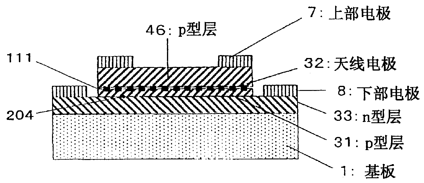
图3是表示本发明的实施方式3的面型调制器的结构的图。FIG. 3 is a diagram showing the configuration of an area modulator according to
图4是表示本发明的实施方式2的面型调制器的结构的图。FIG. 4 is a diagram showing the configuration of an area modulator according to
图5是表示本发明的实施方式5的面型调制器的结构的图。FIG. 5 is a diagram showing the configuration of an area modulator according to
图6是表示本发明的面型调制器的安装方法的图。Fig. 6 is a diagram showing a mounting method of the area modulator of the present invention.
图7是表示本发明的面型调制器的安装方法的图。Fig. 7 is a diagram showing a mounting method of the area modulator of the present invention.
图8是表示本发明的面型调制器的安装方法的图。Fig. 8 is a diagram showing a mounting method of the area modulator of the present invention.
图9是表示使用了本发明的面型调制器的系统的图。Fig. 9 is a diagram showing a system using the area modulator of the present invention.
图10是表示使用了本发明的实施方式4、6的面型调制器的调制方式的图。FIG. 10 is a diagram showing a modulation method using an area modulator according to Embodiments 4 and 6 of the present invention.
图11是表示本发明的实施方式1的面型调制器的调制原理的图。FIG. 11 is a diagram showing the modulation principle of the area modulator according to
图12是表示现有的面型调制器的结构的图。FIG. 12 is a diagram showing the structure of a conventional area modulator.
图13是表示本发明的实施方式1的面型调制器的制造方法的图。13 is a diagram showing a method of manufacturing the area modulator according to
图14是表示本发明的实施方式1、2、3的面型调制器结构的变形例的图。FIG. 14 is a diagram showing a modified example of the structure of the area modulator according to
图15是表示本发明的实施方式6的面型调制器的结构的图。FIG. 15 is a diagram showing the configuration of an area modulator according to Embodiment 6 of the present invention.
图16是表示本发明的实施方式5的面型调制器的制造方法的图。16 is a diagram showing a method of manufacturing the area modulator according to
图17是表示本发明的实施方式6的面型调制器的制造方法的图。FIG. 17 is a diagram showing a method of manufacturing an area modulator according to Embodiment 6 of the present invention.
图18是表示使用了本发明的面型调制器的信息插座的结构的图。Fig. 18 is a diagram showing the structure of an information jack using the area modulator of the present invention.
具体实施方式Detailed ways
下面,参照附图说明本发明的实施方式。Hereinafter, embodiments of the present invention will be described with reference to the drawings.
(实施方式1)(Embodiment 1)
作为本发明的半导体发光元件的实施方式1,图1表示具有折射率调整层的面型调制器结构。As
下面,对该元件的制造方法、结构和动作方法进行说明。设入射光的波长为1.3μm。首先,如图13(a)所示,在n型InP基板1上通过MOVPE法等外延生成不掺杂下部反射层2、掺杂了Si的n型InP下部接触层3(厚100nm)、折射率调整层4、掺杂了Zn的p型InP上部接触层5(厚100nm)、不掺杂上部反射层6。下部反射层2和上部反射层6分别是由5对In0.8Ga0.2P层(厚λ/4、格子失真-1%)和InAs0.2P0.8层(厚λ/4、格子失真1%)构成的失真量子阱结构。不有意添加不纯物、不掺杂是为了抑制电荷带吸收和自由电子吸收。折射率调整层4是由8对不掺杂InP层(厚10nm)和不掺杂In0.9Ga0.1As0.2P0.8层(厚10nm、格子失真偏离-1的1%)构成的失真量子阱结构。之后,如图13(b)所示,堆积SiO2膜53,并蚀刻成圆形来作为蚀刻掩膜后,使用该蚀刻掩膜并通过硫酸系蚀刻剂蚀刻成圆筒状直到到达上部接触层5。这是因为其在形成引导光的圆形区域的同时,尽可能减小了折射率调整层4的面积并提高了动作速度的缘故。这里,InAsP层中蚀刻速度快,而形成上部反射层的InGaP层和上部与下部InP层的势垒层的蚀刻速度是相同的。但是,因InGaP层膜厚薄并且因来自InAsP层的As扩散,其蚀刻速度比InP层快。因此,蚀刻可有选择地停止在上部接触层5。之后,如图13(c)所示,堆积SiO2膜54,蚀刻成圆形并作为蚀刻掩膜后,使用该蚀刻掩膜,通过盐酸系蚀刻剂来蚀刻去除上部接触层5。之后,通过硫酸系蚀刻剂来蚀刻去除折射率调整层4。这时,由于构成折射率调整层4的InP层薄为10nm,并从InGaAsP扩散了As,所以可通过硫酸系蚀刻剂进行蚀刻。结果,如图13(c)所示,在下部接触层3上,可选地停止了蚀刻。之后,蒸镀Cr/Pt/Au电极来作为上部电极7,蒸镀Au-Sn电极来作为下部电极8,通过抬升(lift off),如图13(d)那样形成而得到图1所示的结构。另外,下部反射层2、折射率调整层4和上部反射层6的结构虽然并不限于上述这样,但是需要折射率调整层4的量子阱结构的势垒层和阱层的能带隙比下部反射层2和上部反射层6的量子阱结构的势垒层和阱层的能带隙小。Next, the manufacturing method, structure and operation method of this element will be described. Let the wavelength of the incident light be 1.3 μm. First, as shown in Fig. 13(a), an undoped lower
下面,使用图11说明该元件的动作方法。如图11(a)所示,在没有施加电压的情况下,将折射率调整层4的吸收端波长设为1.28μm。这时的折射率(n’)为(n’=3.2)<(n=3.6)。对1.3μm的光,反射层的距离(d/n’)为1.1μm,由于设定了折射率调整层的厚度(d)与光的波长(nλ)相同而不能使得d/n=λ=1.3μm成立,所以光透过了。另一方面,如图11(b)所示,通过施加5V左右的反偏压,并由弗朗兹—凯尔迪什效应而将吸收端的波长加到1.29μm,从而由InGaAsP层构成的折射率调整层4的折射率增大到5.0左右。结果,反射层2、6间的多层膜的总折射率增加到n=3.6,对1.3μm的光,其距离变为1.3μm,而在反射层2、6间形成驻波,并通过反射层整体来进行反射。即,下部反射层2和上部反射层4的间隔在光学上与信号光的波长相同。结果,由于反射了光,所以很难透过。进一步,若施加大的反偏压,则如图11(c)所示,下部反射层2和上部反射层6的间隔在光学上比信号光的波长长,由于很难反射光,所以透过光的强度增加。由图10(d)的虚线(类型B)来表示所输出的相对电信号的光信号。由此可以明白,在电信号从ON变为OFF,或者从OFF变为ON时显示出光强度减小这一特性。将电信号的开始状态从OFF决定为ON,若测量光信号减弱的脉冲,则可明白电信号是ON还是OFF。在该调制方式时,因为即使电信号的上升和下降特性劣化了,也可同样形成光脉冲,所以可进行良好的传送。另外,若进一步增大所施加的反偏压到10V以上,则会通过折射率调整层4发生光吸收,并进一步减小透过光的强度。Next, the operation method of this element will be described using FIG. 11 . As shown in FIG. 11( a ), when no voltage was applied, the absorption end wavelength of the refractive index adjustment layer 4 was set to 1.28 μm. The refractive index (n') at this time is (n'=3.2)<(n=3.6). For the light of 1.3 μm, the distance (d/n') of the reflection layer is 1.1 μm, because the thickness (d) of the refractive index adjustment layer is set to be the same as the wavelength (nλ) of the light, it cannot make d/n=λ= 1.3μm holds true, so light gets through. On the other hand, as shown in Figure 11(b), by applying a reverse bias voltage of about 5V and increasing the wavelength of the absorption end to 1.29 μm by the Franz-Keldish effect, the refraction of the InGaAsP layer The refractive index of the index adjustment layer 4 increases to about 5.0. As a result, the total refractive index of the multilayer film between the
另一方面,在n型反射层中将Si、在p型反射层中将Zn仅掺杂到InGaP层,而具有导电性时,虽然多少有一些电荷带吸收和自由电子吸收,元件结构和制造方法变得极其简单。如图14(a)所示,通过MOVPE法等在p型InP基板1上外延生成掺杂了Zn的p型下部反射层2、折射率调整层4、掺杂了Si的n型上部反射层6。上部反射层6选择n型是因为n型中载流子充分扩展,故可期待受光区域整个面上有均匀的特性的缘故。下部反射层2和上部反射层6分别由5对掺杂了Si或Zn的InGaP层(厚λ/4)和不掺杂的InAsP层(厚λ/4)构成。折射率调整层4由8对不掺杂InP层(厚10nm)和不掺杂InGaAsP层(厚10nm)构成。之后,在受光区域上堆积SiO2膜,蚀刻成圆形并作为蚀刻掩膜,并使用该蚀刻掩膜通过硫酸系蚀刻剂进行蚀刻直到到达下部反射层2。这时,由于不能可选地停止蚀刻,所以由蚀刻时间控制蚀刻到达下部反射层2。之后,在形成了In2O3透明电极55后,通过蒸镀Au-Sn上部电极7和在基板里面蒸镀Cr/Pt/Au下部电极8并抬升而形成。由于动作方法与图1的结构相同,故在此省略。On the other hand, when the n-type reflective layer is doped with Si and the p-type reflective layer with Zn only to the InGaP layer and has conductivity, although there is some charge band absorption and free electron absorption, the device structure and manufacturing The method becomes extremely simple. As shown in FIG. 14(a), a p-type lower
将调制器的上部电极7的开口区域设为圆形,并将来自光纤的光入射到开口区域。下面,将作为该光的透过区域的上部电极7的开口区域称为受光区域。也可将下部反射层6的直径设为光纤的芯线大小+套管的余地。在为单模式光纤时,由于芯线为几μm,所以上部反射层6的直径可以是10μm左右。另外,下部电极8接近于折射率调整层4形成,覆盖着下部接触层(图中没有示出)。下部电极8和折射率调整层4的间隔最好在10μm以下。这是因为考虑到虽然通常将来自光纤的光入射到上部电极7的开口区域内,但是当光纤的线芯形状大时,会覆盖上部电极7的一部分。因此,可将上部电极7的宽度设为10μm以上,使得来自光纤的光不会漏到上部电极7的外部。但是,在不具有充分的光纤轴的情况下,存在光漏到了上部电极7外部的情况。这时将下部电极8和折射率调整层4的间隔设为10μm以下,尽可能使光由下部电极8反射并不会透过。The opening area of the
另一方面,如图14(a)所示,在基板里面形成了电极的情况下,将下部电极8的内径做得比上部电极7的外径小。这时,即使在不具有充分的光纤轴的情况下,相对光的入射方向下部电极8和上部电极7重合,使得光不会漏到上部电极7的外侧,即,尽可能使光由下部电极8反射并不会透过。On the other hand, as shown in FIG. 14( a ), when electrodes are formed inside the substrate, the inner diameter of the lower electrode 8 is made smaller than the outer diameter of the
下面对面型调制器的安装方法和使用了面型调制器的系统结构进行说明。这些部分由于在下面所有的实施方式中同样可以使用,所以以本实施方式为代表进行说明,其后的实施方式中采用相同结构。The installation method of the area modulator and the system configuration using the area modulator will be described below. Since these portions can be used similarly in all the following embodiments, this embodiment will be described as a representative, and the same configuration will be adopted in the following embodiments.
图6表示通过本实施方式制作的面型调制器的安装方法。如图所示,通过焊接附着下部电极8而与固定夹具9的附着n侧电极40的焊锡10固定。另外,上部电极7通过使用电极带连接到固定夹具的p侧电极41。之后,在该状态下,如图7(a)所示,除了将该固定夹具9与电子电路22连接之外,还与光敏二极管21一起,铸模到连接层23上。光敏二极管通过接收来自光纤26的泄漏光而进行动作。通过将支撑光纤26的套圈25插入到连接层23中并进行锁定,而成为图7(b)所示的形态。同轴电缆24为10Gbps的以太标准。这里,如图7(b)所示,光纤26通过具有同一中心轴的形状而接触面型调制器。结果,若通过现有的连接层来连接光纤,也同样很容易,插入外部调制器也是可能的。FIG. 6 shows a mounting method of the surface modulator produced in this embodiment. As shown in the figure, the lower electrode 8 is fixed to the solder 10 with the n-side electrode 40 of the fixing jig 9 by soldering. In addition, the
另一方面,现有的模块结构如图7(c)所示,由于使用了波导路径型调制器44,所以需要将从两条光纤输出的光光学耦合到截面为1μm角度的波导路径带(stripe)上。所以,需要在调制器的两侧分别插入一个透镜43,共插入两个而将光导入到波导路径。结果,在光纤26-透镜43、透镜43-调制器44、调制器44-透镜43’,透镜43’-光纤26的四个位置上需要采用光学结合。要采取光学结合,需要在一个位置上耗费数分钟,同时需要将光纤等的部件固定到模块上,对于波导路径型调制器的制作而言,需要许多工时。另一方面,在面型调制器的情况下,由于形成了与光纤的芯线粗细相同或者比其大的调制区域,所以如图7(a)所示,接上光纤即可,制造工作量少,价格低廉、并适合小型化。就是出现故障的情况下,只卸下光纤就可以容易地进行替换。On the other hand, in the existing module structure as shown in Fig. 7(c), since a waveguide path modulator 44 is used, it is necessary to optically couple the light output from the two optical fibers to a waveguide strip ( stripe). Therefore, it is necessary to insert one lens 43 on both sides of the modulator, and insert two lenses 43 in total to guide the light into the waveguide. As a result, optical coupling needs to be used at four positions of fiber 26-lens 43, lens 43-modulator 44, modulator 44-lens 43', lens 43'-fiber 26. To adopt optical coupling, it takes several minutes at one position, and at the same time, components such as optical fibers need to be fixed to the module, and many man-hours are required for the manufacture of waveguide-type modulators. On the other hand, in the case of a planar modulator, since a modulation area equal to or larger than the core wire thickness of the optical fiber is formed, as shown in FIG. Less, cheap, and suitable for miniaturization. That is, in the event of a failure, it can be easily replaced by simply removing the fiber.
进一步,在使用了多模光纤或者塑料光纤时,芯线的大小变大。例如,塑料光纤的话,会大到100μm左右。这时,若将上部反射层的大小设为100μm,则调制器的面积变大,调制器的寄生电容也就增大了。如图8(a)所示,通过使用前端为球状的光纤,可以将来自图7的光纤的出射光从图8(b)原封不动的状态变成图8(c)那样将光聚在一起,从而减小了调制器的受光面积,实现了低电容化,即,使高速动作成为可能。通过将受光区域设为50μm以下,而使10Gbps以上的动作成为可能。在此,如果是受光区域和上部反射层的位置错开的情况,由于透过了光,所以如图1(b)所示,用电极金属覆盖元件的几乎整个面,来抑制来自上部反射层的区域以外的透过光。Furthermore, when a multimode optical fiber or a plastic optical fiber is used, the size of the core becomes large. For example, plastic optical fibers can be as large as about 100 μm. At this time, if the size of the upper reflective layer is set to 100 μm, the area of the modulator becomes larger, and the parasitic capacitance of the modulator also increases. As shown in Fig. 8(a), by using an optical fiber with a spherical tip, it is possible to change the emitted light from the optical fiber in Fig. 7 from the state in Fig. Together, thereby reducing the light-receiving area of the modulator, realizing low capacitance, that is, making high-speed operation possible. By reducing the light-receiving area to 50 μm or less, it becomes possible to operate at 10 Gbps or more. Here, if the positions of the light-receiving region and the upper reflective layer are shifted, since the light is transmitted, as shown in FIG. Transmitted light outside the area.
作为本实施方式的调制器的动作方法,在没有施加电压时,调制器为ON状态,通过施加5V以上的电压,调制器变为OFF状态。在该调制方法中,由于折射率调整层没有吸收光,因而也没有生成/消灭电荷,所以使得不受载流子速度影响的高速开关成为可能。即使在10Gpbs时眼形图的打开传送也成为可能。As an operating method of the modulator of this embodiment, when no voltage is applied, the modulator is in the ON state, and when a voltage of 5 V or more is applied, the modulator is in the OFF state. In this modulation method, since the refractive index adjustment layer does not absorb light and thus does not generate/destroy charges, high-speed switching independent of carrier velocity is possible. Open transmission of the eye diagram is possible even at 10Gpbs.
图18表示本实施方式的信息插座的结构。信息插座62在家用插座的上部设置了信息线(10Gbps以太网络连接)67用的插入口72。这里,使用组装入了信息线67的信息插头71,使得在连接电源线(100V)68用接头的同时,连接信息线。信息线67由防护套72、信号用地线65和信号线66构成,现有的地线与防护线相同。将光信号变换为电信号后,直接通过单芯的电缆结构将其传送到设备。因此,不能像双绞线那样进行全双工通信。FIG. 18 shows the structure of the information outlet of this embodiment. The information outlet 62 is provided with an insertion port 72 for the information line (10Gbps Ethernet connection) 67 on the upper part of the household outlet. Here, the information plug 71 incorporating the information line 67 is used so that the information line is connected simultaneously with the connector for the power line (100V) 68 . The information line 67 is composed of a protective cover 72, a signal ground line 65, and a signal line 66, and the conventional ground line is the same as the protective line. After the optical signal is converted into an electrical signal, it is directly transmitted to the device through a single-core cable structure. Therefore, full-duplex communication cannot be performed like twisted-pair cables.
图9表示使用了本实施方式的调制器的光传送系统。使用访问系光纤(单模光纤)40从载流子站传送来的光信号暂时用下行PD36接收光,并变换为下行电信号62。通过该下行电信号来调制面型调制器LD69。这里,通过DC驱动使用端面发光型的1.3μm半导体激光器。在将下行信号传送到各设备时,将除面型调制器LD69之外的所有面型调制器设为ON(透明),并通过内置在各连接中的光敏二极管21(图7)接收光,并作为电信号从10Gbps以太的同轴电缆24(图7)提供给各设备。由于下行信号即使是高传送率也为1Gbps左右,所以对于通过10Gbps传送的LAN内的传送进一步还要有追加信号的余量。并使用该空闲时间进行各个连接间的传送。即,在没有下行信号的情况下,面型调制器LD69原样不动地置为ON,例如,通过面型调制器20A调制DC光,并通过面型调制器20D的受光元件接收该信号。相反,在将信号从面型调制器20D传送到面型调制器20A时,则暂时由LAN用PD38接收光,并在变换为电信号LAN64进行存储后,使用下行信号的间隙调制面型调制器LD69后进行发送,而由面型调制器A进行接收。另外,在将光信号发送到LAN外部时,通过由LAN用PD38变换的上行电信号63调制上行用LD。本系统的特征是形成了光纤环路。其结果,发光元件有一个即可,系统的可靠性提高的同时,还能够通过使用比激光器廉价的面型调制器使系统的价格降低。另外,作为发光元件,不仅可以是激光器,还可使用价格低廉的发光二极管。这是因为发光二极管的强度与发光面积成正比。因此,使用面积大的面型调制器可以调制强度更强的信号光。进一步,由于面型调制器为连接类型,所以可容易进行元件的交换和追加,同时,还可容易分析故障模式。另外,为了形成环路,不仅可容易实现各连接间的通信,而且还不需要光开关等,因而可降低媒体转换器的价格。另外,调制器表面或里面由电极覆盖,形成了抑制光的结构,所以光纤可以使用大口径的POF光纤。FIG. 9 shows an optical transmission system using the modulator of this embodiment. The optical signal transmitted from the carrier station using the access optical fiber (single-mode optical fiber) 40 is temporarily received by the downlink PD 36 and converted into a downlink electrical signal 62 . The area modulator LD69 is modulated by the downlink electric signal. Here, an end-emitting type 1.3 μm semiconductor laser is used by DC driving. When transmitting the downstream signal to each device, set all the area modulators except the area modulator LD69 to ON (transparent), and receive light through the photodiode 21 (Fig. 7) built in each connection, And it is supplied as an electrical signal from the 10 Gbps Ethernet coaxial cable 24 (FIG. 7) to each device. Since the downlink signal has a transmission rate of about 1 Gbps even at a high transmission rate, there is still room for an additional signal for transmission within a LAN transmitted at 10 Gbps. And use this idle time for transmission between connections. That is, when there is no downlink signal, the area modulator LD69 is turned ON as it is, for example, DC light is modulated by the area modulator 20A, and the signal is received by the light receiving element of the area modulator 20D. On the contrary, when the signal is transmitted from the area modulator 20D to the area modulator 20A, the light is temporarily received by the PD38 for LAN, and after being converted into an electrical signal LAN64 for storage, the area modulator is modulated using the gap of the downlink signal. Send after LD69, and receive by area modulator A. In addition, when transmitting an optical signal to the outside of the LAN, the uplink LD is modulated by the uplink electrical signal 63 converted by the LAN PD 38 . The characteristic of this system is that an optical fiber loop is formed. As a result, only one light-emitting element is required, and the reliability of the system is improved, and the cost of the system can be reduced by using an area modulator which is cheaper than a laser. In addition, not only lasers but also inexpensive light-emitting diodes can be used as light-emitting elements. This is because the intensity of an LED is directly proportional to the area where it emits light. Therefore, signal light with stronger intensity can be modulated by using a large area modulator. Furthermore, since the area modulator is a connection type, replacement and addition of components can be easily performed, and at the same time, failure modes can be easily analyzed. In addition, in order to form a loop, it is not only easy to realize communication between each connection, but also does not require optical switches, etc., so the price of the media converter can be reduced. In addition, the surface or inside of the modulator is covered with electrodes to form a light-suppressing structure, so the optical fiber can use a large-diameter POF optical fiber.
(实施方式2)(Embodiment 2)
图2表示本发明的实施方式2的调制器的结构图。下面,说明该元件结构和动作方法。FIG. 2 shows a configuration diagram of a modulator according to
如图2(a)(b)所示,本实施方式的调制器包括基板1。在基板1上形成n型半导体层33(下面,简记为n型层33),在该n型层33上形成p型半导体层31(下面,简记为p型层31)和下部电极8。下部电极8在n型层33上形成,并在中央具有圆形开口。另一方面,p型层31具有直径比下部电极8的开口的内径还小的圆形平面形状,并形成与该下部电极8的开口内的开口为同轴状。因此,在p型层31和下部电极8之间形成了一定间隙。在p型层31上经天线电极32配置p型半导体层46(下面,简记为p型层46)。因此,在p型层31和p型层46之间形成空隙111。P型层46和天线电极32具有与p型层31有同一直径的圆形平面形状,并配置为与p型层31同轴状。如图2(d)所示,在俯视图中,天线电极32形成为没有交点102的网状。即,配置天线电极32,使得通过假想的网的交点102彼此分离的节点(导体片)101作为整体形成网。这里,该网具有正方形的网孔,因此,配置节点101使其作为整体形成格子形状。当将信号光的波长设为λ时,将节点101的宽度W2设定为λ/3左右,将节点101的宽度方向的间隔W1设为λ左右。这里,信号光(入射光)的波长λ为1.5μm。As shown in FIG. 2( a ) and ( b ), the modulator of this embodiment includes a
如图2(a)(b)所示,在p型层46上形成上部电极7。上部电极7具有与p型层46有相同外形的圆形环状的平面形状,并与p型层46同轴状配置。并且,基板1、n型层33、p型层31和p型层46由透光性的材料构成,下部电极8和上部电极7由不透光性的材料构成。并且,信号光从基板1的下面射入,从p型层46的上面射出。As shown in FIG. 2( a )( b ),
接下来,对如上构成的调制器的制造方法进行说明。Next, a method of manufacturing the modulator configured as above will be described.
参照图2(a),(d),首先,通过MOVPE法等在半绝缘体GaAs基板1上外延生成掺杂了Si的n型GaAs层33(厚200nm)、p型GaAs层31(厚10nm)。之后,形成如图2(d)所示的天线电极32。作为构成天线电极32的金属,虽然使用了W,但是如果是高熔点的金属,也并不限于此。之后,使p型GaAs层46和p型GaN层31的表面密合,在含有氢气的氮气环境中在400℃以上的温度下保持1分钟,从而经天线电极32与在其他GaAs基板上生长的p型GaAs层46熔合。虽然熔合温度比起通常结晶的熔合要低,但由于是经过了由W构成的天线电极32的熔合,所以可认为即使是低温,也可因金属的催化反应而产生熔合反应。如图2(a)所示,这里,两层p型层分离开,其间具有空间111。结果,在使天线电极32具有作为天线的功能的区域111中,为了在折射率为1的空气中传播光,电极间隔λ/n由于成为λ而变好,所以处理变得容易。Referring to Fig. 2 (a), (d), at first, by MOVPE method etc. on
接着,将SiO2膜作为掩膜,而将p型层46和p型层31蚀刻为短圆筒状。这是为了在形成引导光的圆形受光区域的同时,尽量减小pn结204的界面面积,提高动作速度。最后,分别在p型层46上蒸镀由Cr/Pt/Au构成的上部电极7,在n型层33上蒸镀由Au/Ge构成的下部电极8并抬升,得到图2(a)所示的结构。Next, using the SiO 2 film as a mask, the p-
下面,说明如上构成、制造的调制器的动作。Next, the operation of the modulator configured and manufactured as described above will be described.
在图2(c)中,在p型层31和n型层33间的pn结(下面,仅称为pn结)204的两侧形成耗尽层203。在没有将电压施加到上部电极7和下部电极8之间的状态下,该耗尽层203形成夹着pn结204的狭窄区域(图中没有示出)。参照图2(d),在该状态下,天线电极32中,由于通过p型层31,46各节点101彼此导通,所以具有作为天线的功能。因此,由于从基板1的下面入射,并通过空隙111的信号光是电磁波,所以通过天线电极32被反射。调制器的透光量就减小了。In FIG. 2( c ), depletion layers 203 are formed on both sides of a pn junction (hereinafter, simply referred to as pn junction) 204 between p-
另一方面,若在上部电极7和下部电极8之间施加为pn结204反偏压的电压(下面,称为反偏压),则位于p型层31和n型层33的pn结204的两侧区域上的耗尽层203变宽。这里,掺杂由GaAs构成的n型层33使得不纯物浓度为1018cm-3,掺杂由GaAs构成的p型层31,46使得不纯物浓度为2×1017cm-3,由此,耗尽层203在不纯物浓度低的p型层31,46侧大大变宽。因此,图2(c)中仅表示了p型层31,46侧的耗尽层203。该耗尽层203从p型层31经天线电极32向p型层46变扩展。参照图2(d),在该状态下,由于天线电极32的各节点101耗尽交点102并没有彼此导通,所以对电磁波的相位没有影响,没有作为天线的功能。由此,可增大调制器的透光量。On the other hand, if a voltage (hereinafter, referred to as reverse bias voltage) is applied between the
因此,该设备通过开/关上部电极7和下部电极8之间的反偏压电压,可减小/增大该信号光的透光量,从而具有作为调制器的功能。Therefore, the device can reduce/increase the transmitted light amount of the signal light by turning on/off the reverse bias voltage between the
这里,若施加2V的反偏压,则耗尽层203从pn结204开始扩展至100nm的范围,由此,如图2(c)所示,完全耗尽p型层31,还部分耗尽p型层46。因此,需要将反偏压施加为2V以上。Here, if a reverse bias voltage of 2V is applied, the depletion layer 203 extends from the
如上所说明的,本实施方式的调制器在没有施加电压时为OFF(反射)状态,若施加了2V以上的电压时,则为ON(透过)。即,在OFF时,反射入射光,并降低输出光量,所以在ON时可得到大的输出强度。另外,在ON/OFF时,由于在该调制器中,仅耗尽层203的快速动作决定动作速度,所以可容易实现10Gbps以上的动作速度。As described above, the modulator of this embodiment is in an OFF (reflective) state when no voltage is applied, and is in an ON (transmissive) state when a voltage of 2 V or more is applied. That is, when it is OFF, incident light is reflected and the output light quantity is reduced, so a large output intensity can be obtained when it is ON. In addition, in this modulator, only the rapid operation of the depletion layer 203 determines the operating speed during ON/OFF, so an operating speed of 10 Gbps or higher can be easily realized.
另外,在该调制器中,在信号光的波长在天线电极32的宽度方向的间隔W1=λ以上时,信号光全部被反射,所以不依赖于波长的调制器就成为可能。In addition, in this modulator, when the wavelength of the signal light is greater than or equal to the interval W1 in the width direction of the
图14(b)是表示本实施方式的变形例的截面图。Fig. 14(b) is a cross-sectional view showing a modified example of the present embodiment.
在本实施方式中,在可以存在由自由电子造成的损失时,作为基板1也可使用导电性基板,例如n型GaAs基板,来代替半绝缘性GaAs基板。这时,如图14(b)所示,可在基板1的里面设置下部电极8。In this embodiment, when losses due to free electrons may exist, a conductive substrate such as an n-type GaAs substrate may be used as the
另外,在本实施方式中,虽然天线电极32具有正方形的网孔,但是网孔也可以是任何形状。In addition, in the present embodiment, although the
另外,天线电极32的材料并不限于金属,只要具有导电性即可,例如也可以是掺杂了不纯物而具有导电性的半导体。In addition, the material of the
另外,天线电极的周围的介质可以不是空气,由其他电介质构成也可以。即,设置电介质层来代替图2(a)的空隙111,可以将天线电极32位于该电介质层中。这时,为了加宽天线电极32的节点间隔,电介质层的折射率n最好接近于1。In addition, the surrounding medium of the antenna electrode may not be air, but may be made of other dielectric medium. That is, a dielectric layer is provided instead of the void 111 in FIG. 2( a ), and the
另外,基板1也可以由例如InP构成。这时,耐压会提高。In addition, the
另外,也可以在基板1上形成p型层,并在其上形成含有天线电极的n型层。Alternatively, a p-type layer may be formed on the
另外,也可以将p型层31和p型层46当作一体,在厚度方向上将n型层33分割为二,并在其间设置空隙111和天线电极32。Alternatively, the p-
(实施方式3)(Embodiment 3)
图3(a)表示本发明的实施方式3的调制器的结构图。下面,说明该元件的制造方法和结构。入射光的波长设为1.3μm。如图3(b)所示,在半绝缘性GaAs基板1上通过MOVPE法等反复外延生长nipi结构。该nipi结构是由以下各部分反复生长而来的:掺杂了Si的n型AlGaAs层12(103nm厚)、添加了由10层构成的载流子限制器用杂质的半绝缘性GaAs/AlGaAs-MQW层(5nm+5nm)14、掺杂了Mg的p型AlGaAs层13(103nm厚)、半绝缘性MQW层14。n型AlGaAs层12和p型AlGaAs层13的Al组成与半绝缘性GaAs/AlGaAs-MQW层14的平均Al组成相同。AlGaAs层13和半绝缘性MQW层14的层厚的和为λ/2。FIG. 3( a ) shows a configuration diagram of a modulator according to
之后,如图3(c)所示,通过蚀刻来除去两个侧面。进一步,如图3(d)所示,由扩散或者离子注入在各个侧面上形成n型重掺杂层49、n型轻掺杂层50、p型轻掺杂层51、p型重掺杂层52。结果,重掺杂区域形成作为各个导电型区域的n型区域47和p型区域48,另外,在轻掺杂区域中,在与掺杂剂相同导电型的部位上维持该导电型。在导电型相反的区域中成为共掺杂,而成为高阻抗区域(半导体的连接区域201)。另外,由于半绝缘性结晶部位通过载流子限制器用掺杂剂抵消载流子,所以仍是半绝缘性。其结果,所有的n型层与n型区域相连,所有的p型层与p型区域相连,同时,n型层和p型层通过半绝缘性MQW分离绝缘,图3(a)的结构就形成了。Afterwards, as shown in FIG. 3(c), both sides are removed by etching. Further, as shown in FIG. 3( d), an n-type heavily doped
另外,在自由电子造成的损失被允许的状况下,导电性基板可使用例如n型GaAs基板。结果,如图14(c)所示,也可在基板里面设置具有圆形透过区域的下部电极。Also, as the conductive substrate, for example, an n-type GaAs substrate can be used under the condition that loss due to free electrons is allowed. As a result, as shown in FIG. 14(c), a lower electrode having a circular transmissive region can also be provided inside the substrate.
下面表示动作方法。在没有施加电压的情况下,由于n型AlGaAs层12、p型AlGaAs层13和半绝缘性MQW层14都具有相同的平均Al组成,所以折射率不改变,可作为同一物质捕捉光,所以不进行反射。但是,通过在n型电极15和p型电极16之间施加反偏压,半绝缘性MQW层14上就施加了电场,因量子封闭效应,只有半绝缘性MQW层14的折射率增大了,故出现了周期结构,起到反射层作用。结果,由于反射了入射光,减小了透过光,所以可作为外部调制器动作。这时的动作原理是半绝缘性MQW层14上产生电场,而并非光被吸收,所以不产生载流子。结果,在调制器OFF时,由于反射了入射光,而降低了输出光量,所以在ON时可得到大的输出强度。另外,实现了与耗尽层动作速度相同的设备动作速度,即10Gbps以上。The operation method is shown below. When no voltage is applied, since the n-
另外,也可由InGaAsP构成n型层12和p型层13,由InP/InGaAsP-MQW构成半绝缘性MQW14。这时,需要使n型层12、p型层13和半绝缘性MQW14的GaAs的组成比例一定。另外,需要使Ga和As的比为1∶2。Alternatively, the n-
(实施方式4)(Embodiment 4)
图4(a)表示本发明的实施方式4的调制器的结构图。下面,说明该元件的制造方法和结构。入射光的波长设为1.3μm。如图4(a)所示,在蓝宝石基板1上生成了GaN低温势垒层(图中没有示出)后,通过MOVPE法外延生成掺杂了2×1018cm-3的Si的n型GaN下部接触层3(厚4μm)、Al0.5Ga0.5N/In0.1Ga0.9N带间吸收层17,掺杂了Mg的p型GaN上部接触层5(厚500nm)。该带间吸收层17由5层构成,由掺杂了5×1018cm-3的AlGaN势垒层(厚3nm)和掺杂了5×1017cm-3的AlGaN阱层(厚2nm)反复生长而成的。之后,在整个面上蒸镀了Ni(厚5nm)/Au(厚10nm)的上部透明电极7后,将SiO2作为掩膜,并在喷涂了上部透明电极7后,通过氯系干式蚀刻来蚀刻去除直到上部接触层5、带间吸收层17。进一步,蒸镀Al/Pt/Au下部电极8,得到图4(a)的结构。FIG. 4(a) shows a configuration diagram of a modulator according to Embodiment 4 of the present invention. Next, the manufacturing method and structure of this element will be described. The wavelength of incident light was set to 1.3 μm. As shown in Figure 4(a), after a GaN low-temperature barrier layer (not shown in the figure) is formed on the
另外,在自由电子造成的损失被允许的状况下,也可使用例如n型GaN基板或者n型SiC基板来作为导电性基板1。结果,如图4(b)所示,可在基板里面设置下部电极8。In addition, an n-type GaN substrate or an n-type SiC substrate can also be used as the
表示动作方法。如图4(c)所示,在没有施加电压的状态下,传送带的带不连续量为1.5eV左右。这时的一次能量状态E1为阱层以上0.3eV左右。这里,设阱层的压电电场为6.5MV/cm,势垒层的压电电场为-6.5MV/cm。由于两次能量状态E2为阱层以上1.2eV,所以所吸收的光的波长为1.37μm左右,1.3μm的光被吸收。另一方面,如图4(d)所示,若在电极7、8之间施加5V的电压,则向各阱层施加1V的电场,等价地阱层的厚度变为1/2,一次的能量状态E1成为0.4eV。另外,两次的能量状态E2变为1.4V,而上升到势垒层的电平附近。结果,所吸收的光的波长减短为1.24μm左右,而使得透过1.3μm波长的光。这里,虽然没有施加电压时带间能量差为1.37μm,但是由于不与能带产生谐振,所以不吸收。因此,若施加2.5V电压,使得带间能量和光的能量相同,则如图10(b)所示,在阱层中1.3μm的光就会被吸收。这时的调制光的强度被调制为如图10(d)的虚线(类型B)所示的那样。由于吸收光谱的半值幅度为30meV左右,所以因施加了2.5V的电压而造成的光谱偏移就可得到充分的消光比。这里,在带间吸收时,由于载流子在传导带内能量消失,所以载流子寿命就变得很短,与电场吸收型时的情况不同,能够进行高速动作。Indicates an action method. As shown in FIG. 4( c ), in the state where no voltage is applied, the belt discontinuity amount of the conveyor belt is about 1.5 eV. The primary energy state E1 at this time is about 0.3 eV above the well layer. Here, it is assumed that the piezoelectric field of the well layer is 6.5 MV/cm, and the piezoelectric field of the barrier layer is -6.5 MV/cm. Since the secondary energy state E2 is 1.2 eV above the well layer, the wavelength of the absorbed light is about 1.37 μm, and the light of 1.3 μm is absorbed. On the other hand, as shown in Figure 4(d), if a voltage of 5V is applied between the
(实施方式5)(Embodiment 5)
图5(a)表示本发明的实施方式5的调制器的结构图。下面,说明该元件的制造方法和结构。入射光的波长设为1.3μm。如图16(a)所示,通过MOVPE法等在半绝缘性InP基板1上外延生成掺杂了Si的n型InP下部接触层3(厚100nm)、不掺杂耗尽区调整层74、掺杂了Zn的p型InP上部接触层5(厚100nm)。耗尽区调整层74由5对不掺杂InP层(厚10nm)和不掺杂InGaAsP层(厚5nm)构成。之后,如图16(b)所示,堆积SiO2膜,蚀刻成圆形作为蚀刻掩膜53,并使用该蚀刻掩膜通过盐酸系蚀刻剂蚀刻去除比上部电极7还外侧的InP上部接触层5后,用硫酸系蚀刻剂进行蚀刻直到下部接触层3。这里也如实施方式1所说明的,可选地蚀刻耗尽区调整层74,并且蚀刻到下部接触层3停止。之后,如图16(c)所示,改为堆积SiO2膜54,并将受光区域设为蚀刻的蚀刻掩膜,并使用该蚀刻掩膜,通过盐酸系蚀刻剂来蚀刻去除受光区域的上部接触层。之后,如图16(d)所示,以200nm左右的间隔将直径为2nm的多个金圆点19配置在受光区域,其上部由SiO2保护。下面表示金圆点19的形成方法。首先,将受光区域的不掺杂耗尽区调整层的表面浸泡到硅烷偶联剂材料(APTES)等的5%溶液中。之后,将Au胶体溶液滴到表面,放置1小时左右。在除去Au胶体溶液后,进行水洗和干燥,在100℃下进行烘烤。之后,为了除去表面的有机物,用氧等离子在60℃60W下进行清洁处理10分钟。之后,在320℃下使用等离子CVD堆积SiO2。由于这次要形成直径2nm的Au圆点19,所以为了设为2.5×109cm2,而将pH设为8-9。在Au圆点19为5nm时,将pH设为9-10左右。表面的金圆点19的间隔需要选择比吸收光的耗尽区调整层74的内部波长短的间隔。这里,设耗尽区调整层74的折射率为3.2,金圆点19的间隔为小于400nm。之后,蒸镀Cr/Pt/Au电极作为上部电极7,蒸镀Au-Sn电极作为下部电极8,通过抬升而如图16(d)那样形成,得到图5(a)所示的结构。FIG. 5(a) shows a configuration diagram of a modulator according to
下面,说明该元件的动作方法。在没有施加电压的情况下,由于不掺杂耗尽区调整层74表示为1017cm-3左右的n型,所以不形成等离子体激元。另一方面,若将电压施加到耗尽区调整层74,耗尽区调整层74耗尽,如图5(c)所示,在耗尽区域调整层74的内部的对应于金圆点19的区域上形成了等离子体激元。在形成了该等离子体激元的位置(即,等离子体激元形成区域58)中,由于折射率变大,所以在折射率调制周期上光谐振而被吸收。Next, the operation method of this element will be described. When no voltage is applied, since the undoped depletion
另一方面,在基板1中具有导电性的情况下,如图5(b)所示,虽然多少存在电荷带吸收和自由电子吸收,但元件结构和制造方法变得极其简单。通过MOVPE法等外延生成不掺杂耗尽区调整层74、掺杂了Zn的p型InP上部接触层5(厚100nm)。之后,如图16(b)所示,堆积SiO2膜,蚀刻成圆形而作为蚀刻掩膜53,在使用该蚀刻掩膜通过盐酸系蚀刻剂蚀刻去除了比上部电极7还外侧的InP上部接触层5后,通过硫酸系蚀刻剂有选择地进行蚀刻直到基板1。之后,进行与图16相同的工序,最后在基板里面蒸镀下部电极8,并通过抬升,来形成下部电极8。由于动作方法与图5(a)的结构相同,所以在此省略。On the other hand, when the
(实施方式6)(Embodiment 6)
图15(a)表示本实施方式6的调制器的结构图。下面,说明该元件的制造方法和结构。入射光的波长设为1.3μm。如图17(a)所示,在n型InP基板1上以10-30nm的间隔堆积直径为2nm的多个下部金圆点18,并通过喷涂来堆积厚度为λ/4的100nm的InP59。再次堆积下部金圆点18’,并进一步通过喷涂而在λ/4的厚度上堆积InP59’从而得到图17(b)。这里,两层的InP层虽然没有意进行掺杂,但是,由于目的是从下部金圆点18进行放电,所以两层都要以表示5×1017cm-3左右的n型导电性作为堆积条件。另一方面,如图17(c)所示,在另一InP基板58上依次生成作为上部接触层的掺杂了Zn的p型InP层5(厚100nm)和不掺杂折射率调整层4。折射率调整层4由8个周期的不掺杂InP层(厚10nm)和不掺杂InGaAsP层(厚10nm)构成。之后,反转图17(c)的基板而使其接触在图17(b)的基板上,并在400℃下在含有氢气的环境中进行加热熔化。结果,得到图17(d)。在通过使用机械化学抛光和盐酸系蚀刻剂的蚀刻而除去基板58后,如图17(e)所示,堆积SiO2膜,并蚀刻成圆形来作为蚀刻掩膜,并且使用该蚀刻掩膜通过盐酸系蚀刻剂来蚀刻去除了比上部电极7还外侧的InP上部接触层5后,通过硫酸系蚀刻剂进行蚀刻直到不掺杂InP膜59’。这里也如实施方式1所说明的,可选地蚀刻折射率调整层4,并在不掺杂InP膜中停止蚀刻。之后,在受光区域上堆积上部金圆点19,并用不掺杂InP膜进行覆盖。虽然上部金圆点19的形成方法与实施方式5相同,但是为了除去表面的有机物,用氧等离子在60℃60W下进行清洁处理10分钟后,在室温下通过喷涂堆积InP。由于这次使用了直径为2nm的Au圆点,所以为了设为2.5×1011cm2,而设PH为5-7。在Au圆点为5nm的情况下,pH为2-3左右。下部金圆点18’和上部金圆点19的间隔为360nm,与1.3μm的光相对应。由于该不掺杂InP膜60也用于金圆点的放电,所以将表示5×1017cm-3左右的n型导电性作为堆积条件。如上即得到了图15(a)的结构。FIG. 15(a) shows a configuration diagram of a modulator according to the sixth embodiment. Next, the manufacturing method and structure of this element will be described. The wavelength of incident light was set to 1.3 μm. As shown in FIG. 17(a), a plurality of lower gold dots 18 with a diameter of 2nm are deposited at intervals of 10-30nm on the n-
下面,说明该元件的动作方法。这里,取代在实施方式1中所用的反射层,使用金圆点18、19。金圆点18、19其自身具有许多载流子,同时在不掺杂InP层内也形成许多等离子体激元。结果,如实施方式1所示,即使不重叠多层的反射层也可得到充分的效果。即,通过在下段形成两层、在上段形成一层金圆点18、19,可得到光裂缝结晶的效果。这是因为由于多个金圆点18、19分别间隔10-30nm进行非常紧密地排列,形成了三维的光裂缝结晶的缘故。在没有施加电压的情况下,设折射率调整层4的吸收端波长为1.28μm。Next, the operation method of this element will be described. Here, gold dots 18 and 19 are used instead of the reflective layer used in
这时的折射率为3.2。对于1.3μm的光上下金圆点18、19之间的距离为1.15μm,由于光的波长不为λ=1.3μm,则光由于金圆点反射而不会透过。另一方面,通过施加5V左右的反偏压,而通过弗朗兹—凯尔迪什效应来将吸收端的波长增大到1.29μm,由此使InGaAsP层的折射率增大为5.0左右。结果,金圆点层18、19间的多层膜的总的折射率增大到3.6,相对于1.3μm的光,距离变为1.3μm,在金圆点18、19之间形成驻波,而使得光透过。另外,若大于该电压,则金圆点18、19间的距离与波长相比过长,光就被反射了。由于该现象就是所谓的三维的光裂缝能带隙现象,所以波长范围是浮动的,故可适应频谱宽的发光二极管等。结果,就得到如图10(a)所示的透过特性,通过图10(c)的信号所调制的光信号成为图10(d)的实线(类型A)所描画的形状。The refractive index at this time was 3.2. For 1.3 μm light, the distance between the upper and lower gold dots 18 and 19 is 1.15 μm. Since the wavelength of the light is not λ=1.3 μm, the light will not pass through due to the reflection of the gold dots. On the other hand, by applying a reverse bias voltage of about 5 V, the wavelength at the absorption end is increased to 1.29 μm by the Franz-Keldish effect, thereby increasing the refractive index of the InGaAsP layer to about 5.0. As a result, the total refractive index of the multilayer film between the gold dot layers 18, 19 increases to 3.6, with respect to the light of 1.3 μm, the distance becomes 1.3 μm, forming a standing wave between the gold dots 18, 19, allowing light to pass through. In addition, if it exceeds this voltage, the distance between the gold dots 18 and 19 is too long compared with the wavelength, and the light is reflected. Since this phenomenon is the so-called three-dimensional optical crack bandgap phenomenon, the wavelength range is floating, so it can be applied to light-emitting diodes with a wide spectrum. As a result, the transmission characteristic shown in FIG. 10(a) is obtained, and the optical signal modulated by the signal in FIG. 10(c) has the shape drawn by the solid line (type A) in FIG. 10(d).
作为本领域内技术人员,从上面的说明中,可得到本发明的多个改进和其他实施方式。因此,上述说明应解释为仅作为示例,其目的是给本领域内技术人员提供实施本发明的最佳实施方式。实质上可改变其结构和/或功能的细节,而不脱离本发明的精神。As those skilled in the art, many improvements and other implementations of the present invention can be obtained from the above description. Therefore, the above description should be construed as an example only, and its purpose is to provide those skilled in the art with the best mode for carrying out the invention. Details of its structure and/or function may be changed substantially without departing from the spirit of the invention.
产业上的可利用性Industrial availability
本发明的面型调制器在作为用于光通信系统等的光调制器方面有用。The area modulator of the present invention is useful as an optical modulator used in an optical communication system or the like.
本发明的面型调制器的制造方法在用于光通信系统等的光调制器的制造方法方面有用。The method of manufacturing an area modulator of the present invention is useful as a method of manufacturing an optical modulator used in an optical communication system or the like.
Claims (14)
Applications Claiming Priority (2)
| Application Number | Priority Date | Filing Date | Title |
|---|---|---|---|
| JP2002000336 | 2002-01-07 | ||
| JP336/2002 | 2002-01-07 |
Publications (2)
| Publication Number | Publication Date |
|---|---|
| CN1545634A CN1545634A (en) | 2004-11-10 |
| CN1237369C true CN1237369C (en) | 2006-01-18 |
Family
ID=19190477
Family Applications (1)
| Application Number | Title | Priority Date | Filing Date |
|---|---|---|---|
| CNB038008807A Expired - Fee Related CN1237369C (en) | 2002-01-07 | 2003-01-07 | Surface light modulator and manufacturing method thereof |
Country Status (5)
| Country | Link |
|---|---|
| US (2) | US6778308B2 (en) |
| JP (1) | JP3589662B2 (en) |
| CN (1) | CN1237369C (en) |
| AU (1) | AU2003202467A1 (en) |
| WO (1) | WO2003058327A1 (en) |
Families Citing this family (16)
| Publication number | Priority date | Publication date | Assignee | Title |
|---|---|---|---|---|
| US7083993B2 (en) * | 2003-04-15 | 2006-08-01 | Luminus Devices, Inc. | Methods of making multi-layer light emitting devices |
| US20100289721A1 (en) * | 2004-10-12 | 2010-11-18 | Guy Silver | Em rectifying antenna suitable for use in conjunction with a natural breakdown device |
| JP2006259064A (en) * | 2005-03-16 | 2006-09-28 | Fdk Corp | Method and device for electric field enhancement by surface plasmon |
| FR2887373B1 (en) * | 2005-06-17 | 2007-08-10 | Thales Sa | OPTOELECTRONIC COMPONENT COMPRISING A SEMICONDUCTOR OPTICAL GUIDE WITH AN ENHANCED OPTICAL INDEX ACTIVE HEART |
| KR100944743B1 (en) * | 2005-07-08 | 2010-03-03 | 파나소닉 전공 주식회사 | Base unit for double wiring system |
| KR101198763B1 (en) * | 2006-03-23 | 2012-11-12 | 엘지이노텍 주식회사 | Post structure and LED using the structure and method of making the same |
| EP2094602A2 (en) * | 2006-11-20 | 2009-09-02 | Nxp B.V. | A sealing structure and a method of manufacturing the same |
| EP2219523B1 (en) * | 2007-11-08 | 2013-03-06 | Inolact Ltd. | Measuring fluid excreted from an organ |
| DE102011005422B4 (en) * | 2011-03-11 | 2013-01-31 | Ihp Gmbh - Innovations For High Performance Microelectronics / Leibniz-Institut Für Innovative Mikroelektronik | Electro-optical modulator |
| EP2853867A4 (en) * | 2012-05-16 | 2016-01-20 | Hamamatsu Photonics Kk | PHOTODETECTOR |
| WO2013172269A1 (en) * | 2012-05-16 | 2013-11-21 | 浜松ホトニクス株式会社 | Photodetector |
| US9891769B2 (en) * | 2014-11-25 | 2018-02-13 | Lg Innotek Co., Ltd. | Touch window |
| KR102542466B1 (en) * | 2015-11-27 | 2023-06-12 | 삼성전자주식회사 | Beam steering device and system employing the same |
| JP7147378B2 (en) * | 2018-08-30 | 2022-10-05 | Tdk株式会社 | antenna |
| CN109817828A (en) * | 2019-01-25 | 2019-05-28 | 重庆石墨烯研究院有限公司 | A kind of graphene transparent electrode and its work function regulate and control method |
| CN116097156A (en) * | 2020-08-13 | 2023-05-09 | 华为技术有限公司 | Design and manufacturing method for membrane modulator device |
Family Cites Families (13)
| Publication number | Priority date | Publication date | Assignee | Title |
|---|---|---|---|---|
| US4828368A (en) * | 1986-06-30 | 1989-05-09 | Hughes Aircraft Company | Near bandgap radiation modulation spatial light modulators |
| JPH0793473B2 (en) * | 1987-10-06 | 1995-10-09 | 古河電気工業株式会社 | Optical semiconductor device |
| US5008717A (en) * | 1989-03-03 | 1991-04-16 | At&T Bell Laboratories | Semiconductor device including cascaded modulation-doped quantum well heterostructures |
| US5034783A (en) * | 1990-07-27 | 1991-07-23 | At&T Bell Laboratories | Semiconductor device including cascadable polarization independent heterostructure |
| JPH05152674A (en) | 1991-11-25 | 1993-06-18 | Nec Corp | Surface light emitting semiconductor laser with outer modulator |
| JP2936880B2 (en) * | 1992-04-06 | 1999-08-23 | 松下電器産業株式会社 | Polarizer and digital modulator using the same |
| US5309531A (en) * | 1992-11-12 | 1994-05-03 | California Institute Of Technology | Broad-band substrate-wave-coupled electro-optic modulator |
| JP3369778B2 (en) * | 1995-03-23 | 2003-01-20 | 松下電器産業株式会社 | Semiconductor reflective multilayer film and reflective spatial light modulator |
| JPH11103135A (en) | 1997-07-30 | 1999-04-13 | Mitsubishi Cable Ind Ltd | Board for gallium nitride crystal growth, and its application |
| JPH11133365A (en) * | 1997-10-29 | 1999-05-21 | Yazaki Corp | Tunable filter and method of manufacturing the same |
| US6219170B1 (en) * | 1998-07-13 | 2001-04-17 | Fuji Photo Film Co., Ltd. | Light modulation device, exposing device and display unit |
| US6252221B1 (en) * | 1999-06-21 | 2001-06-26 | Agilent Technologies, Inc. | Photo-conductive switch having an improved semiconductor structure |
| JP2001066559A (en) * | 1999-08-25 | 2001-03-16 | Matsushita Electric Ind Co Ltd | Light modulator |
-
2003
- 2003-01-07 CN CNB038008807A patent/CN1237369C/en not_active Expired - Fee Related
- 2003-01-07 AU AU2003202467A patent/AU2003202467A1/en not_active Abandoned
- 2003-01-07 JP JP2003558580A patent/JP3589662B2/en not_active Expired - Fee Related
- 2003-01-07 WO PCT/JP2003/000004 patent/WO2003058327A1/en not_active Ceased
- 2003-09-02 US US10/652,044 patent/US6778308B2/en not_active Expired - Fee Related
-
2004
- 2004-07-13 US US10/889,027 patent/US6917457B2/en not_active Expired - Fee Related
Also Published As
| Publication number | Publication date |
|---|---|
| AU2003202467A1 (en) | 2003-07-24 |
| US6917457B2 (en) | 2005-07-12 |
| WO2003058327A1 (en) | 2003-07-17 |
| US20040080803A1 (en) | 2004-04-29 |
| JP3589662B2 (en) | 2004-11-17 |
| CN1545634A (en) | 2004-11-10 |
| US6778308B2 (en) | 2004-08-17 |
| US20040257632A1 (en) | 2004-12-23 |
| JPWO2003058327A1 (en) | 2005-05-19 |
| WO2003058327A8 (en) | 2004-11-25 |
Similar Documents
| Publication | Publication Date | Title |
|---|---|---|
| CN1237369C (en) | Surface light modulator and manufacturing method thereof | |
| US10305250B2 (en) | III-Nitride nanowire array monolithic photonic integrated circuit on (001)silicon operating at near-infrared wavelengths | |
| CN101510665B (en) | Laser, module, optical transmission device, optical transmission device and system | |
| US7680162B2 (en) | Long wavelength vertical cavity surface emitting laser device and method of fabricating the same | |
| CN1714485A (en) | Low voltage multi-junction vertical cavity surface emitting laser | |
| CN114175281B (en) | Light emitting element and method for manufacturing light emitting element | |
| JPH09172229A (en) | Transparent substrate vertical resonance type surface luminescence laser manufactured by semiconductor wafer bonding | |
| CN104769467A (en) | Semiconductor device | |
| CN110970797B (en) | High-speed high-bandwidth vertical cavity surface emitting laser | |
| US8611392B2 (en) | Semiconductor laser | |
| CN211929898U (en) | Vertical cavity surface emitting laser device | |
| US8798112B2 (en) | High speed lasing device | |
| CN113422295B (en) | A multi-junction distributed feedback semiconductor laser and its fabrication method | |
| US7638792B2 (en) | Tunnel junction light emitting device | |
| WO2014126164A1 (en) | Semiconductor optical element, semiconductor laser element, manufacturing method therefor, and method for manufacturing semiconductor laser module and semiconductor element | |
| US5925896A (en) | Surface-emitting semiconductor optical device | |
| CN110112653B (en) | Vertical external cavity surface emitting semiconductor laser | |
| CN115085006B (en) | Long wavelength VCSEL with combined reflectors at two ends and preparation method thereof | |
| CN112366518A (en) | Distributed feedback laser and preparation method thereof | |
| CN113745968A (en) | Semiconductor laser and preparation method thereof | |
| CN1922518A (en) | Buried heterostructure device fabricated by single step MOCVD | |
| JP4526548B2 (en) | Surface light modulator | |
| CN215771900U (en) | Multi-junction distributed feedback semiconductor laser | |
| CN112615257A (en) | Laser epitaxial structure, manufacturing method thereof and VCSEL chip | |
| CN118801210B (en) | A high-power anti-reflection semiconductor laser |
Legal Events
| Date | Code | Title | Description |
|---|---|---|---|
| C06 | Publication | ||
| PB01 | Publication | ||
| C10 | Entry into substantive examination | ||
| SE01 | Entry into force of request for substantive examination | ||
| C14 | Grant of patent or utility model | ||
| GR01 | Patent grant | ||
| C17 | Cessation of patent right | ||
| CF01 | Termination of patent right due to non-payment of annual fee |
Granted publication date: 20060118 Termination date: 20140107 |