CN1237387C - Method for roll-to-roll display fabrication by simultaneous lithographic exposure on a substrate support web - Google Patents

Method for roll-to-roll display fabrication by simultaneous lithographic exposure on a substrate support web Download PDF

Info

Publication number
CN1237387C
CN1237387C CNB011396121A CN01139612A CN1237387C CN 1237387 C CN1237387 C CN 1237387C CN B011396121 A CNB011396121 A CN B011396121A CN 01139612 A CN01139612 A CN 01139612A CN 1237387 C CN1237387 C CN 1237387C
Authority
CN
China
Prior art keywords
photomask
supporting network
miniature cup
ring
radiation
Prior art date
Legal status (The legal status is an assumption and is not a legal conclusion. Google has not performed a legal analysis and makes no representation as to the accuracy of the status listed.)
Expired - Fee Related
Application number
CNB011396121A
Other languages
Chinese (zh)
Other versions
CN1371023A (en
Inventor
陈美英
陈仙海
吴让二
张小加
臧宏玫
梁荣昌
Current Assignee (The listed assignees may be inaccurate. Google has not performed a legal analysis and makes no representation or warranty as to the accuracy of the list.)
HIBEX IMAGE LLC
Original Assignee
HIBEX IMAGE LLC
Priority date (The priority date is an assumption and is not a legal conclusion. Google has not performed a legal analysis and makes no representation as to the accuracy of the date listed.)
Filing date
Publication date
Priority claimed from US09/784,972 external-priority patent/US6933098B2/en
Application filed by HIBEX IMAGE LLC filed Critical HIBEX IMAGE LLC
Publication of CN1371023A publication Critical patent/CN1371023A/en
Application granted granted Critical
Publication of CN1237387C publication Critical patent/CN1237387C/en
Anticipated expiration legal-status Critical
Expired - Fee Related legal-status Critical Current

Links

Images

Classifications

    • GPHYSICS
    • G02OPTICS
    • G02FOPTICAL DEVICES OR ARRANGEMENTS FOR THE CONTROL OF LIGHT BY MODIFICATION OF THE OPTICAL PROPERTIES OF THE MEDIA OF THE ELEMENTS INVOLVED THEREIN; NON-LINEAR OPTICS; FREQUENCY-CHANGING OF LIGHT; OPTICAL LOGIC ELEMENTS; OPTICAL ANALOGUE/DIGITAL CONVERTERS
    • G02F1/00Devices or arrangements for the control of the intensity, colour, phase, polarisation or direction of light arriving from an independent light source, e.g. switching, gating or modulating; Non-linear optics
    • G02F1/01Devices or arrangements for the control of the intensity, colour, phase, polarisation or direction of light arriving from an independent light source, e.g. switching, gating or modulating; Non-linear optics for the control of the intensity, phase, polarisation or colour 
    • G02F1/165Devices or arrangements for the control of the intensity, colour, phase, polarisation or direction of light arriving from an independent light source, e.g. switching, gating or modulating; Non-linear optics for the control of the intensity, phase, polarisation or colour  based on translational movement of particles in a fluid under the influence of an applied field
    • G02F1/166Devices or arrangements for the control of the intensity, colour, phase, polarisation or direction of light arriving from an independent light source, e.g. switching, gating or modulating; Non-linear optics for the control of the intensity, phase, polarisation or colour  based on translational movement of particles in a fluid under the influence of an applied field characterised by the electro-optical or magneto-optical effect
    • G02F1/167Devices or arrangements for the control of the intensity, colour, phase, polarisation or direction of light arriving from an independent light source, e.g. switching, gating or modulating; Non-linear optics for the control of the intensity, phase, polarisation or colour  based on translational movement of particles in a fluid under the influence of an applied field characterised by the electro-optical or magneto-optical effect by electrophoresis
    • GPHYSICS
    • G02OPTICS
    • G02FOPTICAL DEVICES OR ARRANGEMENTS FOR THE CONTROL OF LIGHT BY MODIFICATION OF THE OPTICAL PROPERTIES OF THE MEDIA OF THE ELEMENTS INVOLVED THEREIN; NON-LINEAR OPTICS; FREQUENCY-CHANGING OF LIGHT; OPTICAL LOGIC ELEMENTS; OPTICAL ANALOGUE/DIGITAL CONVERTERS
    • G02F1/00Devices or arrangements for the control of the intensity, colour, phase, polarisation or direction of light arriving from an independent light source, e.g. switching, gating or modulating; Non-linear optics
    • G02F1/01Devices or arrangements for the control of the intensity, colour, phase, polarisation or direction of light arriving from an independent light source, e.g. switching, gating or modulating; Non-linear optics for the control of the intensity, phase, polarisation or colour 
    • G02F1/13Devices or arrangements for the control of the intensity, colour, phase, polarisation or direction of light arriving from an independent light source, e.g. switching, gating or modulating; Non-linear optics for the control of the intensity, phase, polarisation or colour  based on liquid crystals, e.g. single liquid crystal display cells
    • G02F1/133Constructional arrangements; Operation of liquid crystal cells; Circuit arrangements
    • G02F1/1333Constructional arrangements; Manufacturing methods
    • G02F1/133305Flexible substrates, e.g. plastics, organic film
    • GPHYSICS
    • G02OPTICS
    • G02FOPTICAL DEVICES OR ARRANGEMENTS FOR THE CONTROL OF LIGHT BY MODIFICATION OF THE OPTICAL PROPERTIES OF THE MEDIA OF THE ELEMENTS INVOLVED THEREIN; NON-LINEAR OPTICS; FREQUENCY-CHANGING OF LIGHT; OPTICAL LOGIC ELEMENTS; OPTICAL ANALOGUE/DIGITAL CONVERTERS
    • G02F1/00Devices or arrangements for the control of the intensity, colour, phase, polarisation or direction of light arriving from an independent light source, e.g. switching, gating or modulating; Non-linear optics
    • G02F1/01Devices or arrangements for the control of the intensity, colour, phase, polarisation or direction of light arriving from an independent light source, e.g. switching, gating or modulating; Non-linear optics for the control of the intensity, phase, polarisation or colour 
    • G02F1/13Devices or arrangements for the control of the intensity, colour, phase, polarisation or direction of light arriving from an independent light source, e.g. switching, gating or modulating; Non-linear optics for the control of the intensity, phase, polarisation or colour  based on liquid crystals, e.g. single liquid crystal display cells
    • G02F1/133Constructional arrangements; Operation of liquid crystal cells; Circuit arrangements
    • G02F1/1333Constructional arrangements; Manufacturing methods
    • G02F1/133377Cells with plural compartments or having plurality of liquid crystal microcells partitioned by walls, e.g. one microcell per pixel
    • GPHYSICS
    • G02OPTICS
    • G02FOPTICAL DEVICES OR ARRANGEMENTS FOR THE CONTROL OF LIGHT BY MODIFICATION OF THE OPTICAL PROPERTIES OF THE MEDIA OF THE ELEMENTS INVOLVED THEREIN; NON-LINEAR OPTICS; FREQUENCY-CHANGING OF LIGHT; OPTICAL LOGIC ELEMENTS; OPTICAL ANALOGUE/DIGITAL CONVERTERS
    • G02F1/00Devices or arrangements for the control of the intensity, colour, phase, polarisation or direction of light arriving from an independent light source, e.g. switching, gating or modulating; Non-linear optics
    • G02F1/01Devices or arrangements for the control of the intensity, colour, phase, polarisation or direction of light arriving from an independent light source, e.g. switching, gating or modulating; Non-linear optics for the control of the intensity, phase, polarisation or colour 
    • G02F1/165Devices or arrangements for the control of the intensity, colour, phase, polarisation or direction of light arriving from an independent light source, e.g. switching, gating or modulating; Non-linear optics for the control of the intensity, phase, polarisation or colour  based on translational movement of particles in a fluid under the influence of an applied field
    • G02F1/1675Constructional details
    • G02F1/1679Gaskets; Spacers; Sealing of cells; Filling or closing of cells
    • GPHYSICS
    • G02OPTICS
    • G02FOPTICAL DEVICES OR ARRANGEMENTS FOR THE CONTROL OF LIGHT BY MODIFICATION OF THE OPTICAL PROPERTIES OF THE MEDIA OF THE ELEMENTS INVOLVED THEREIN; NON-LINEAR OPTICS; FREQUENCY-CHANGING OF LIGHT; OPTICAL LOGIC ELEMENTS; OPTICAL ANALOGUE/DIGITAL CONVERTERS
    • G02F1/00Devices or arrangements for the control of the intensity, colour, phase, polarisation or direction of light arriving from an independent light source, e.g. switching, gating or modulating; Non-linear optics
    • G02F1/01Devices or arrangements for the control of the intensity, colour, phase, polarisation or direction of light arriving from an independent light source, e.g. switching, gating or modulating; Non-linear optics for the control of the intensity, phase, polarisation or colour 
    • G02F1/165Devices or arrangements for the control of the intensity, colour, phase, polarisation or direction of light arriving from an independent light source, e.g. switching, gating or modulating; Non-linear optics for the control of the intensity, phase, polarisation or colour  based on translational movement of particles in a fluid under the influence of an applied field
    • G02F1/1675Constructional details
    • G02F1/1679Gaskets; Spacers; Sealing of cells; Filling or closing of cells
    • G02F1/1681Gaskets; Spacers; Sealing of cells; Filling or closing of cells having two or more microcells partitioned by walls, e.g. of microcup type
    • GPHYSICS
    • G03PHOTOGRAPHY; CINEMATOGRAPHY; ANALOGOUS TECHNIQUES USING WAVES OTHER THAN OPTICAL WAVES; ELECTROGRAPHY; HOLOGRAPHY
    • G03FPHOTOMECHANICAL PRODUCTION OF TEXTURED OR PATTERNED SURFACES, e.g. FOR PRINTING, FOR PROCESSING OF SEMICONDUCTOR DEVICES; MATERIALS THEREFOR; ORIGINALS THEREFOR; APPARATUS SPECIALLY ADAPTED THEREFOR
    • G03F7/00Photomechanical, e.g. photolithographic, production of textured or patterned surfaces, e.g. printing surfaces; Materials therefor, e.g. comprising photoresists; Apparatus specially adapted therefor
    • G03F7/0005Production of optical devices or components in so far as characterised by the lithographic processes or materials used therefor
    • G03F7/0007Filters, e.g. additive colour filters; Components for display devices
    • GPHYSICS
    • G03PHOTOGRAPHY; CINEMATOGRAPHY; ANALOGOUS TECHNIQUES USING WAVES OTHER THAN OPTICAL WAVES; ELECTROGRAPHY; HOLOGRAPHY
    • G03FPHOTOMECHANICAL PRODUCTION OF TEXTURED OR PATTERNED SURFACES, e.g. FOR PRINTING, FOR PROCESSING OF SEMICONDUCTOR DEVICES; MATERIALS THEREFOR; ORIGINALS THEREFOR; APPARATUS SPECIALLY ADAPTED THEREFOR
    • G03F7/00Photomechanical, e.g. photolithographic, production of textured or patterned surfaces, e.g. printing surfaces; Materials therefor, e.g. comprising photoresists; Apparatus specially adapted therefor
    • G03F7/20Exposure; Apparatus therefor
    • G03F7/2035Exposure; Apparatus therefor simultaneous coating and exposure; using a belt mask, e.g. endless
    • GPHYSICS
    • G03PHOTOGRAPHY; CINEMATOGRAPHY; ANALOGOUS TECHNIQUES USING WAVES OTHER THAN OPTICAL WAVES; ELECTROGRAPHY; HOLOGRAPHY
    • G03FPHOTOMECHANICAL PRODUCTION OF TEXTURED OR PATTERNED SURFACES, e.g. FOR PRINTING, FOR PROCESSING OF SEMICONDUCTOR DEVICES; MATERIALS THEREFOR; ORIGINALS THEREFOR; APPARATUS SPECIALLY ADAPTED THEREFOR
    • G03F7/00Photomechanical, e.g. photolithographic, production of textured or patterned surfaces, e.g. printing surfaces; Materials therefor, e.g. comprising photoresists; Apparatus specially adapted therefor
    • G03F7/20Exposure; Apparatus therefor
    • G03F7/24Curved surfaces

Landscapes

  • Physics & Mathematics (AREA)
  • Nonlinear Science (AREA)
  • General Physics & Mathematics (AREA)
  • Optics & Photonics (AREA)
  • Chemical & Material Sciences (AREA)
  • Mathematical Physics (AREA)
  • Crystallography & Structural Chemistry (AREA)
  • Electrochemistry (AREA)
  • Molecular Biology (AREA)
  • Chemical Kinetics & Catalysis (AREA)
  • Life Sciences & Earth Sciences (AREA)
  • Health & Medical Sciences (AREA)
  • Electrochromic Elements, Electrophoresis, Or Variable Reflection Or Absorption Elements (AREA)
  • Devices For Indicating Variable Information By Combining Individual Elements (AREA)

Abstract

本发明涉及一种电泳或液晶显示器及其新颖的制法。本发明的电泳和液晶显示器器件包含有明确定义的形状、尺寸、纵横比的微型杯,分别为分散在具有视觉对比的介电溶剂的带电荷微粒、或用至少一种液晶组分填充。该液晶组分的普通折光系数应与各向同性的微型杯材料相匹配。本发明新颖的“辊对辊”方法和设备,可用同步光刻法连续生产显示器件。其使预定图案、连续环带结构光掩模与预涂布辐射敏感材料的支撑网近距离平行同步移动,辐射源对图像曝露保持定位。该辐射敏感材料可以是一种辐射固化材料,曝光和固化的部分构成微型杯结构。附加处理步骤中,该材料可以是暂时封闭微型杯的正性光刻剂。通过光掩模图像使选定的微型杯组曝光,以选择性地重开、填充、密封。用其它颜色重复,可连续进行组装多色电泳和液晶显示器器件。

Figure 01139612

The present invention relates to an electrophoretic or liquid crystal display and its novel manufacturing method. The electrophoretic and liquid crystal display devices of the present invention comprise microcups of well-defined shape, size, aspect ratio, respectively charged particles dispersed in a visually contrasting dielectric solvent, or filled with at least one liquid crystal component. The general refractive index of the liquid crystal component should match that of the isotropic microcup material. The novel "roll-to-roll" method and equipment of the present invention can continuously produce display devices by synchronous photolithography. It makes the photomask with predetermined pattern, continuous annular band structure and the supporting net of pre-coated radiation-sensitive material move parallel and synchronously at close distance, and the radiation source maintains the position for image exposure. The radiation sensitive material may be a radiation curable material, the exposed and cured portions forming the microcup structure. In an additional processing step, the material can be a positive photoresist that temporarily seals the microcups. Selected microcup sets are exposed through a photomask image to selectively reopen, fill, and seal. Repeating with other colors, multicolor electrophoretic and liquid crystal display devices can be assembled continuously.

Figure 01139612

Description

By carrying out the method that roll-to-roll display is made in the online synchronous photoetching exposure of substrate support
Brief description
The application is one of a series of pending applications of same invention entity application, relates to novel electrophoresis and liquid crystal image display and assembly, and the novel method of making this display and assembly.Some content of this series invention that discloses in these relevant applications also discloses in this application.In this application disclosed any special invention problem content is not proposed claim, can not be interpreted as the applicant and have a mind to abandon patent protection these problem contents.
Invention field
The present invention relates to electrophoretic display device (EPD), particularly make the manufacture method and the technology of the display device of the box that comprises the shape, size and the aspect ratio that clearly define, fill this box with the charged pigment particles that is dispersed in the solvent.Disclosed method be included in carry out synchronous photoetching method exposure on the sensitization supporting network, with roll-to-roll method making electrophoretic display device (EPD).
Background technology related to the present invention
Electrophoretic display device (EPD) is a kind of non-emanative device, and influence is suspended in the principle of the charged pigment particles in the solvent based on electrophoresis.This display plain edition proposed in 1969 first.Typical case's formation of electrophoretic display device (EPD) comprises a pair of staggered relatively, carries out the plate electrode of separated by spaces with the sept that pre-determines distance between two battery lead plates.Usually one of them battery lead plate is transparent.Be packaged with the charged pigment particles of painted solvent and suspension between the two-plate.
When applying a voltage difference between two electrodes, owing to be subjected to having attraction with pigment particle polarity opposite charges pole plate, pigment particle will migrate to this side.Thereby can be charged by the pole plate selectivity, making the color of seeing by transparent polar plate is the color of solvent or the color of pigment particle.Change pole plate polarity, pigment particle can move to relative pole plate, thereby manifests opposite color.Different intermediate color (gray level) is by the density of pigment decision of the transition at transparent polar plate place, can obtain by control voltage and duration of charging.
One of advantage of the flat-panel monitor of relative other type of electrophoretic display device (EPD) is that its power consumption is very low.This outstanding advantage makes electrophoretic display device (EPD) be particularly suitable for portable and battery supply set, for example notebook computer, mobile phone, personal digital assistant, portable electronic medical treatment and diagnostic device, global positioning system apparatus etc.
For fear of undesirable particle migration (for example precipitation), the someone has proposed the way of subregion between two electrodes, and the space between two electrodes is divided into little unit.Referring to M.A.Hopper and V.Novotny, Institute of Electrical and Electric Engineers can be reported-" electronic installation " (IEEE Trans.Electron Device), ED-26,8, pp1148-1152 (1979).Yet, under the situation of partition type electrophoretic display device (EPD), form subregion and suspension encapsulation process and have certain difficulty.In addition, be difficult to make the suspension of different colours to keep separating in the partition type electrophoretic display device (EPD).
Prior art attempts suspension is sealed in the microcapsules.U.S. Patent No. 5,961,804 and U.S. Patent No. 5,930,026 in the electrophoretic display device (EPD) of microencapsulation has been described.These displays have the microcapsules array of primarily two-dimensional, and wherein each microcapsules all contains the electrophoresis component of being made up of dielectric fluid and charged pigment particle suspension (visually forming contrast with dielectric solvent).The formation of these microcapsules can be by means of interfacial polymerization, in-situ polymerization or such as solidifying in physical treatment, the liquid or simple/other known methods such as complicated cohesion.After microcapsules form, can be injected in the box that two isolated electrodes are housed, perhaps with its " printing " or be coated on the transparent conducting film.These microcapsules also can be fixed in the transparent base material or bonding agent, himself can be sandwiched between two pole plates.
Utilize these existing processes, particularly United States Patent (USP) the 5th, 930, and No. 026, the 5th, 961, No. 804 and the 6th, 017, No. 584, there are many shortcomings in the electrophoretic display device (EPD) with the microcapsule method preparation of its disclosure.For example, because the chemical property of microcapsule wall is subjected to the susceptibility susceptibility of humidity and temperature (particularly for) to environmental change, cause the adverse effect of the electrophoretic display device (EPD) that microcapsule method is made.Secondly, because the thin-wall face of capsule and bigger particle size make the electrophoretic display device (EPD) of microcapsule method manufacturing have relatively poor resistance to scraping.For improving the operability of this display, microcapsules are embedded in a large amount of polymeric substrates.But,, make the response time elongated because two electrode separations increase; And, because the low service load of pigment particle reduces contrast.Because charge control agent is tending towards diffusing to water/oily interface during this microcapsules preparation, cause the surface charge density that is difficult to increase pigment particle.The low charge density of pigment particle or zeta potential in the microcapsules also make its sensitivity reduce.In addition, because the big particle size of microcapsules and distribution on a large scale, for color was used, the prior art electrophoretic display device (EPD) of this type had lower resolution and addressing capability.
Summary of the invention
Electrophoretic display device (EPD) of the present invention is made up of the box with shape, size and aspect ratio of clearly defining, and these boxes are filled by the charged pigment particles that is scattered in the dielectric solvent that has visual contrast.
The invention still further relates to a kind of roll-to-roll method and apparatus of novelty, it can make the manufacturing of display carry out continuously by the synchronous photoetching method.Synchronous roll-to-roll method and apparatus also can be used for making LCD (LCD), and other structure and the assembly that are used to make electron device.
One embodiment of the present of invention relate to the making of a plurality of miniature cups, each miniature cup integrally constitutes two-dimensional array jointly as each several part each other, preferably form on supporting network, this supporting network comprises the conducting film of patterning, for example addressable tin indium oxide (ITO) district band.Each miniature cup in the array component all is filled with the suspension that is dispersed in the pigment particle in the dielectric solvent or disperses thing, and forms an electrophoresis cartridge through sealing.
Form the substrate support net of miniature cup thereon, preferably include the display addressing array that contains preformed conducting film (for example ITO conduction region band).Polymer precursor thing floor coating conducting film (ITO district band) and supporting network with radiation curing.This film and precursor layer are carried out graph exposure (detailed description sees below) under radiation, to form the miniature cup wall construction.After the exposure, never exposed areas is removed the precursor material, keeps being bonded in the miniature wall of cup that solidifies on conducting film/supporting network.Can carry out graph exposure with the radiation of ultraviolet light or other form, produce exposure figure or the predetermined pattern that is coated on the radiation curing material on the conducting film by photomask.Although it is normally unwanted, photomask can be positioned and align with conducting film (ITO district band just), space between the transparent like this photomask part alignment ITO district band, opaque photomask part alignment ITO material (preparation becomes the zone at the bottom of the miniature cup box).
In addition, can be coated on thermoplastic or thermoset precursor thing layer on the conducting film with the mold pressing of predetermined pattern punch, the demoulding subsequently prepares the miniature cup array.Can be by radiation, cooling, solvent evaporation or other method sclerosis precursor layer.The pending application application that we submitted on March 4th, 2000, exercise question is for comprising little die pressing method of this novelty in " improved electrophoretic display device (EPD) and novel manufacture method thereof " (AnImproved Electrophoretic Display and Novel Process for ItsManufacture).
Solvent-proof, miniature cup that hot mechanicalness is stable with size, shape and opening ratio of wide region can be with above-mentioned any method preparations.
An alternative embodiment of the invention relates to the miniature cup assembly makes monochromatic electrophoretic display, fills the solid color pigments suspending components in miniature cup, and the sealing miniature cup is at last with stacked this miniature cup array of second conducting film that scribbles adhesive phase in advance.
An alternative embodiment of the invention relates to the method that utilization is opened the miniature cup assembly successively, filled preliminary election miniature cup group, to make color electrophoretic display.The method comprises stacked or be coated with prefabricated miniature cup with positivity effect photoresist, by to positivity effect photoresist graph exposure, after development, optionally open the miniature cup of some, in the miniature cup of opening, fill colored electrophoretic fluid, then the miniature cup of filling with the encapsulating method sealing.Can repeat these steps to make the sealing miniature cup of filling the different colours electrophoretic fluid.Like this, can fill the component of different colours, form colored electrophoretic display device (EPD) at the array of presumptive area.The pigment of various prior aries and dyestuff can be solvent phase and suspended particulates very wide color range of choice are provided.Can adopt the fluid coating and the filling device of prior art.
An alternative embodiment of the invention is that it can be used in the multiple useful technology about the method and apparatus of synchronous roll-to-roll photoetching process exposure, comprises miniature cup array manufacture craft and selects to fill the technology that the miniature cup array forms colored display module.The roll-to-roll photoetching process exposure of figure can be by carrying out well with moved further photomask and sensitization supporting network, so that workpiece (as miniature cup array or chromatic display) carries out graph exposure in continuous and seamless mode.
The photomask of predetermined pattern can be extend, continuously, form the band of ring-type.The corresponding miniature cup array structure of optical mask pattern or other auxiliary equipment are as miniature wall of cup and open top.This photomask makes the figure of miniature cup array structure by the photomask tomographic projection.This " figure " exposure makes the radiation-sensitive materials formation graphic structure that exposes selectively, and the center section material is not exposed.Support and location photomask endless belt with a location device, make photomask and supporting network close, and a part of photomask endless belt is parallel with the part of the supporting network of need exposure basically.
The same moved further of photomask and supporting network comprises near the part of the photomask endless belt of supporting network is parallel with supporting network and moving in the same way.In fact, the photomask endless belt is and the supporting network part of close exposure approaching parallel " rotation " synchronously, keeps figure to locate between exposure period with this.Relevant the moving of supporting network and photomask is in check, and the corresponding construction that is projected between miniature cup pattern on the photomask and exposure period like this on the supporting network keeps the location.A continuous synchronization move with exposure-processed in, supporting network, photomask move with identical speed in same direction between exposure period, to keep this continuous positioning.
In addition, can adopt semicontinuous same moved further, wherein photomask and the supporting network displacement before exposure increases with amount, but is maintained fixed between exposure period.
For roll-to-roll technology, can adopt coupling or feedback circuit or common driving that photomask and supporting network are synchronized with the movement, keep coordinating (promptly moving) with speed.
For the miniature cup array preparation of discrete patterned, this roll-to-roll lithographic exposure apparatus can carry out high speed processing as being with continuously with the conducting film/supporting network that scribbles radiation curable component.After the exposure, supporting network enters the district of developing, and removes unexposed material herein, forms the miniature cup wall construction.Miniature cup and ITO district band preferably has suitable selection size, and coordinates the location with photomask, so can disperse addressing and controlled by display processor of each box of finishing (that just fill with miniature cup sealing).Can be pre-formed ITO district band by carry out wet method or dry method etch technology on the net in substrate support.
For making color monitor,, can be implemented in the miniature cup box group of preliminary election selectivity opening, filling and seal with synchronous roll-to-roll exposure photolithography method of the present invention with the miniature cup array.
Can be with positivity effect photoresist stacked or be coated with the miniature cup array that this is made, thereby temporary sealing miniature cup, miniature cup array to sealing carries out the required miniature cup group open top of graph exposure (for example, using corresponding photomask) selectivity exposure then.Can use the stacked and apparatus for coating of prior art.Can remove the photoresist of exposure, the top of opening selected miniature cup group with developer then.Term in this context " developer " is meant suitable, the selective removal exposure photoresist of prior art, keeps the preparation of unexposed photoresist simultaneously.
Like this, the miniature cup array can be filled the component (generally being three primary colors) of several different colours successively by predetermined box pattern.For example, pattern exposure process can use the positive photoresist top laminate, tentatively seal empty miniature cup.By photomask exposure miniature cup (as, the ring-band shape photomask of describing in the roll-to-roll technology), make it then only to for the first time selected miniature cup group exposure.Remove the photoresist of exposure with the developer development, open first-selected miniature cup group, make it fill the color pigment dispersed component of selection, seal with one of method described herein then.Repeated exposure and developing process make exposure of miniature cup group and the opening selected for the second time, so that fill the pigment dispersing component of selecting for the second time, and sealing then.At last, remove remaining photoresist, carry out the 3rd miniature cup group and fill and seal.
An alternative embodiment of the invention relates to the charged pigment particles that is scattered in electrophoretic fluid disperses thing to fill miniature cup, seals this miniature cup afterwards.Preferably, before filling step, in electrophoretic fluid, disperse a kind of thermoplasticity or thermoset precursors thing to finish sealing.This thermoplasticity or thermoset precursors thing and dielectric solvent are immiscible, and proportion is lower than this solvent and pigment particle.After the filling, thermoplasticity or thermoset precursors thing are separated in electrophoresis liquid, form the floating layer that floats over liquid top.
The sealing of miniature cup can harden the precursor layer by solvent evaporation, interfacial reaction, moisture, heat or radiation easily and finish.Although the combination of two or more aforesaid curing mechanisms can increase the productive capacity of sealing, ultraviolet radiation is most preferred miniature cup encapsulating method.In addition, can finish sealing on the surface of described electrophoretic fluid by the solution coat that will contain thermoplasticity or thermoset precursors thing.In order to reduce or eliminate the internal mix degree during coating is handled, preferably use and do not dissolve each other with electrophoretic fluid and proportion is lower than the sealing component of dielectric fluid.Can precursor be hardened finish sealing by the combination of solvent evaporation, interfacial reaction, moisture, heat, radiation or curing mechanism.These encapsulating methods are features of uniqueness of the present invention.
If replace above-mentioned electrophoretic fluid with having the liquid crystal components suitable and ordinary refractive index that isotropy miniature cup material is complementary, method then of the present invention can be used to make LCD.In miniature cup, press direction of an electric field at " connection " state liquid crystal and be orientated, and be transparent.At " shutoff " state, liquid crystal is irregular alignment, and light is produced scattering.In order to maximize light scattering effect, the diameter of miniature cup is generally 0.5 to 10 micron.
Generally speaking, roll-to-roll technology of the present invention can arrive a plurality of technologies position successively with the guide support net and comes independent continuously supporting network is carried out a series of processing by carrying.
For example, miniature cup can be made successively continuously, fills, sealing and stacked.
Except the making and the filling of miniature cup array, synchronous roll-to-roll technology can be used to prepare multiple structure or discrete pattern, is used for the electronic installation that can form on the supporting network base material, as flexible PCB etc.For technology and the equipment that is used for the electrophoretic display device (EPD) miniature cup described herein, prepare the photomask of a predetermined pattern, it comprises the corresponding photomask ingredient of structural unit of a plurality of and described device.Each such photomask district is can be preselected transparent or to radiation opaque, to form the image of these structural units in the corresponding part of supporting network between exposure period to radiation.Method of the present invention can be used for the selectivity curing of structured material in manufacturing process, or is used for the exposure of positivity or negative effects photo anti-corrosion agent material.
Because the disclosed rapid processing of these multisteps can by roll-to-roll continuously or semicontinuous operation carry out, so be applicable in enormous quantities and low-cost production.With regard to production in enormous quantities, to compare with additive method, these method efficient height and cost are low.Electrophoretic display device (EPD) according to the present invention's making is insensitive to environment, for example humidity and temperature.This display is very thin, flexible, durable, easy to operate, and a great variety of models.Because the shape and size that electrophoretic display device (EPD) according to the present invention has good aspect ratio and clearly defines, bistable reflected displaying device have outstanding color repetitive addressing performance, high-contrast and quick switching rate.In addition, equipment that the present invention is disclosed and method are suitable for the low-cost electrophoretic display device (EPD) of producing in enormous quantities (EPDs), make this electrophoretic display device (EPD) with low energy consumption characteristics to user, scientific research, commercial and industrial electron device bigger applicability be arranged.
Brief Description Of Drawings
Fig. 1 is the diagrammatic cross-section of electrophoretic display device (EPD) of the present invention, is illustrated in three miniature cup boxes that do not apply under the voltage condition.
Fig. 2 is the diagrammatic cross-section of electrophoretic display device (EPD) among Fig. 1, but two tape electricity wherein make granules of pigments migrate to a lateral electrode plate.
Fig. 3 A-3C is the profile with representational one group of miniature cup array of method making of the present invention.Fig. 3 A is a skeleton view, and Fig. 3 B is a vertical view, and Fig. 3 C is a front elevation, in order to represent the clear vertical scale that amplified.
Fig. 4 A-4D is the representative miniature cup array of an a series of the present invention sectional view, and the method for making step of the preferred electrophoretic display device (EPD) of the present invention is described, this example is a monochrome display.
Fig. 5 A and Fig. 5 B diagram are used to prepare the base conditioning step of miniature cup, comprise by photomask (top exposure) and with ultraviolet light the conducting film that is coated with the thermoset precursors thing are carried out figure photoetch exposure.
Fig. 6 A and Fig. 6 B diagram are used to prepare the another kind of treatment step of miniature cup, comprise with ultraviolet light the conducting film that is coated with the thermoset precursors thing is carried out the figure photolithographic exposure, wherein the bottom conductor figure on the transparent substrate replaces photomask (bottom exposure), and to radiation opaque.
Fig. 7 A and Fig. 7 B diagram are carried out the another kind of processing step that miniature cup is made in the exposure of figure photoetching process in conjunction with top exposure and bottom exposure principle, wherein miniature wall of cup exposes at a lateral solidifcation by the photomask top, carry out the bottom exposure by opaque substrate electrically conductive film, solidifying (combination exposure) perpendicular to this horizontal direction.
Fig. 8, Fig. 8 A and Fig. 8 B diagram realize the method step that Fig. 5 A-B handles with the synchronous roll-to-roll photoetching process equipment of novelty of the present invention.
Fig. 9 A prepares the example of multiple colour electrophoretic display with method of the present invention to the 9H diagram.
Figure 10, Figure 10 A and the 10B diagram synchronous roll-to-roll photoetching process equipment of novelty of the present invention, the stacked or coating with positivity effect photoresist, the treatment step of realization Fig. 9 A-H.
Figure 11 schematically illustrates the representational half-continuous process of making a kind of three look electrophoretic display device (EPD) miniature cup array components.
Detailed Description Of The Invention
Hereinafter describe the present invention with the embodiment form, these embodiment can not constitute limitation of the invention.This instructions can make those skilled in the art make and use the present invention, and has described several specific embodiment of the present invention, adjustment, variation, selection and use, comprises the preferred forms of thinking at present.
In this, because complicacy of the present invention, a lot of parts, internal relations and accessory structure are arranged, can not represent clearly simply with a figure, thereby describe by several drawings.Therefore, adopt many synoptic diagram to express, or omit the non-essential part of disclosed the technology of the present invention feature, aspect or principle.Like this, the preferred embodiment of a feature can represent in a figure that the another one feature can be represented in another figure.
Embodiment given herein can make and understand and enforcement the present invention with those skilled in the art know that.These exemplary technologies, method, component and equipment can not be considered to limitation of the scope of the invention, only are used as exemplary illustrated.
The publication and the patented claim of being quoted from the instructions are incorporated herein by reference, and promptly list of references are appointed as in each independent publication or patented claim of mentioning.
Definition
Unless explanation is arranged in this instructions in addition, all technical terms all are the habitual definition that those skilled in the art use and understand usually as used herein.
Term " miniature cup " speech is meant the recess of cup-shaped, can be with making as methods such as little mold pressing or graph exposures.Similarly, plural form in the context " miniature cup " refers generally to the miniature cup combination, comprises that whole formation of a plurality of miniature cups or combination form the miniature cup array of two-dimensional structure.
In the context of the present invention, term " box " refers to by the formed independently unit of a sealing miniature cup.This box is filled with the charged pigment particles that is dispersed in the solvent or in the solvent mixture.
When explanation this miniature cup or the box, term " has clearly definition " and is meant that this miniature cup or box have according to the predetermined clear and definite shape of the special parameter of this technology, size and aspect ratio.
Term " aspect ratio " speech is Essential Terms in the electrophoretic display device (EPD).In this application, be used in term " aspect ratio " on the miniature cup refer to the degree of depth of miniature cup opening and width than or the degree of depth and diameter ratio.
Term " graph exposure " means radiation curing material or photoresist component is carried out radiant exposure, for example use one of method of the present invention to carry out UV (ultraviolet light) radiation, wherein the control material exposed portion is to form pattern or the image corresponding with the miniature cup structure, for example, being limited to corresponding miniature cup wall material and partly exposing, does not expose in the bottom that keeps miniature cup.Under the situation of selectively opened miniature cup array predetermined portions photoresist, graph exposure means and the corresponding part material exposure of miniature cup opening, keeps miniature wall of cup and does not expose.This pattern or image can utilize the mode of photomask exposure to form, or are undertaken by modes such as control particle beams exposures.
Miniature cup array of the present invention and method
Fig. 1 and Fig. 2 are typical miniature cup array component embodiment sectional view synoptic diagram, simplify for clear, provide three miniature cup box 12a, 12b and the 12c of miniature cup array component 10.
As shown in Figure 1, each box 12 of array 10 comprises two battery lead plates 11,13, and it is transparent having an electrode plate 11 at least, tin indium oxide (ITO) electrode for example, and electrode 11,13 constitutes two opposite faces of boxes 12.
Miniature cup box array component 10 is made of a plurality of boxes, and these boxes located adjacent one another arranging in a plane forms the box layer 12 that is encapsulated between two electrode layers 11 and 13.Represented three schematic box 12a, 12b and 12c, by they battery lead plate 11a, 11b and 11c, (transparent panel) and 13a, 13b and 13c (backboard) qualifications separately, be appreciated that, the suitable two-dimensional directional of a plurality of these type of boxes is arranged (in Fig. 1, a left side/the right side on plane and inside/outside direction), form the sheet display device of choosing area and two-dimensional shapes wantonly.Similarly, several miniature cup boxes can be packaged between entire electrode plate 11 or 13, although for clear expression, each box 12 all is encapsulated in and has between the wide single battery lead plate 11 and 13 of single box in Fig. 1.
In the colored dielectric solvent 14 charged pigment particles 15 of disperseing or suspending is arranged, in order to be filled with the clearly box of the shape and size of definition.Each box 12 can be filled the pigment and the solvent (for example being used for monochromatic the demonstration) of same composition, maybe can fill different pigment and solvent composition (for example being used for panchromatic demonstration).Fig. 1 has represented three kinds of different colours combinations, and each box 12a, 12b represent that with different hacures forms solvent is respectively 14a, 4b and 14c with 12c, and pigment particle also is appointed as 15a, 15b, 15c respectively.
Each miniature cup box 12 by sealed wall 16 around form the border (in the plane of array 10, and 17 faces that limit these boxes at the bottom of the miniature cup, in this example, this face is adjacent with electrode 13) of box.Go up (next-door neighbour's electrode 11) each box over there gland bonnet part 18 is all arranged.Here gland bonnet partly is close to transparency electrode 11 (as shown in Figure 1), and gland bonnet 18 is made of clear component.Although in the embodiment in figure 1, at the bottom of the miniature cup 17 and gland bonnet 18 be represented as separately box part, they respectively with contiguous electrode 13 and 11 differences, but at the bottom of the embodiment of miniature cup array 10 of the present invention can comprise the miniature cup of one/electrode structure or gland bonnet/electrode structure.
Fig. 2 is the schematic sectional view of electrophoretic display device (EPD) among Fig. 1, but two boxes (12a and 12c) that add electric charge wherein move on the electrode plate pigment.When between two electrodes 11,13, applying a voltage difference, charged particulate 15 is moved to a side and (is promptly migrated to electrode 11 or 13, the electric charge that depends on particulate and electrode), can see the color of pigment particle 15 or the color of solvent 14 by nesa coating 11 like this.At least two conductors 11 or one of 13 are (addressable areas that separates) of patterning, allow corresponding each box or the predetermined box (as forming a pixel) of certain group to set up the selectivity electric field.
In the example of Fig. 2, shown two box 12a and 12c are charged, and pigment 15a wherein and 15c have moved on to transparent electrode plate 11a and 11c separately.Surplus box 12b keep neutral (pigment 15b is dispersed among the solvent 14b).
Fig. 3 A-3C represents that Fig. 3 A represents a skeleton view with the profile of the canonical dissection of the miniature cup array of method making of the present invention, and Fig. 3 B represents a planimetric map, and Fig. 3 C represents a front view (FV), for clear, has amplified vertical scale.For reflective electrophoretic display, the area of the miniature cup opening that each is independent is preferably about 10 2To 5 * 10 5Square micron is preferably about 10 3To 5 * 10 4Square micron.The width W of miniature cup 12 (distance between the adjacent wall of cup 16) can change in very wide scope, and can select to adapt to final display characteristics.The width W of miniature cup opening (from one side of miniature cup opening to another side) is preferably about 15 to 450 microns, is preferably about 25 to 300 microns.Each miniature cup can constitute the sub-fraction of a pixel of final display, perhaps a complete pixel.
The wall of cup thickness t is relevant with the width W of cup, can in very large range change, and can select to adapt to the characteristics of required final display.The miniature cup wall thickness is generally the miniature cup width and multiply by approximately 0.01 to 1, is preferably the miniature cup width and multiply by about 0.05 to 0.25.Opening is about 0.05 to 100 to the area ratio of wall preferably, is preferably about 0.4 to about 20.
Clear in order to represent, the height h of miniature wall of cup (this size is determined the degree of depth of miniature cup) adopts the proportional sizes of amplifying to represent.Although the wall of cup height has the scope of broad with respect to the width W of cup, optimum height depends on solvent and pigment characteristics and action required electric field.So just can select the wall of cup height, the optimization display is responded characteristic, and does not need with the box width any fixing relation is arranged.The ratio of wall of cup height and little miniature cup width is generally greater than its width ratio with big miniature cup.Usually the wall of cup height is less than the miniature cup width.Preferred miniature cup height about 3 is to about 100 microns, most preferredly is about 10 to about 50 microns.
For ease of simple and clearly description, supposition miniature cup of the present invention is square in the instructions, arranges in the linear two-dimensional mode.Yet miniature cup needn't be required to be square, also can be rectangle, circle or required more complicated shape.For example, miniature cup can be hexagonal, and presses the sexangle close-packed array and arrange, and perhaps, the triangle miniature cup can be orientated and form the sexangle subarray, and it can be sequentially arranged in the sexangle close-packed array.
On the whole, miniature cup can be an Any shape, and their size and dimension can change in whole display.This is favourable in color electrophoretic display.For making visual effect best, can make mixing miniature cup with difformity and size.For example, being filled with the red miniature cup of thing that disperses may be different on shape and size with green miniature cup or blue miniature cup.Further, pixel can be made up of the miniature cup of the varying number of different colours.For example, a pixel can be made up of some little green miniature cup, some big red miniature cup and the little blue miniature cup of some.Concerning three kinds of colors, unnecessary being of similar shape and quantity.
The opening of miniature cup can be circle, square, rectangle, sexangle or any other shape.Spacer area between the opening is as far as possible little, so that keeping gratifying mechanical property simultaneously, obtain high color saturation and contrast.Therefore, other shapes of honey comb like aperture efficiency (for example than circular open) are better.
Adopt the electrophoretic display device (EPD) preparation of miniature cup array
Fig. 4 A-4D schematically illustrates the method for optimizing of preparation miniature cup array.
Shown in Fig. 4 A, miniature cup array 40 can be seen the embodiment shown in Fig. 5,6 and 7 with any one preparation in the optional method of the present invention.The unfilled miniature cup array of method preparation as described herein generally comprises substrate support net 43, has a basal electrode 42 on it.Miniature wall of cup 41 extends upward the formation open cup from substrate support net 43.
Shown in Fig. 4 B, fill miniature cup with the suspension that is dispersed in the charged pigment particles 45 in the painted dielectric solvent component 44.In the example shown, this component all is identical in each glass, is the monochrome display situation.Among Fig. 9 below, illustrative a kind of color monitor assembly, adopt the solvent/pigment component of three kinds of different colours.
Shown in Fig. 4 C, after filling, with a sealant or cap rock 46 sealing miniature cups, it is bonding with miniature wall of cup, stops the solvent leakage.In present a kind of preferred encapsulating method, 46a joins in solvent/pigment component 44/45 with thermoset precursors thing sealing component.Preferred thermoset precursors thing component 46a is not easy to mix in solvent or dissolving, and lower than the proportion of solvent and pigment particle.This thermoset precursors thing 46a separates and forms a surface flotation layer on the top of liquid phase solvent 44.Preferably with this thermoset precursors thing of radiation curing 46a, for example ultraviolet light (or heat and moisture) forms a bonding gland bonnet 46b, seals miniature cup 40 then.In addition, can finish the sealing of miniature cup by directly being coated with on the electrophoretic fluid surface and solidifying one deck thermoset precursors thing component.The detailed description of relevant encapsulating method sees below.
Shown in Fig. 4 D, be laminated in second conducting film 47 on electrophoresis miniature cup box 40 arrays of sealing, the conductor 47 of preferred pre-coating adhesive phase 48, adhesive phase can be contact adhesive, hotmelt or heat, wet or radiation-curing binders.If the top conductive film is transparent to radiation, can be by for example using ultraviolet radiation, pass the top conductive film to stacked bonding agent carry out the back and solidify.
The preparation of pigment/solvent suspension thing or dispersion thing component
To the description of the different embodiment of electrophoretic display device (EPD) of the present invention, preferably fill miniature cup (for example solvent in Fig. 4 B 44 and pigment particle 45) as here with the charged pigment particles that is dispersed in the dielectric solvent.Can disperse thing with the preparation of the existing method in this area, for example U.S. Patent No. 6,017, and 584, No.5,914,806, No.5,573,711, No.5,403,518, No.5,380,362, No.4,680,103, No.4,285,801, No.4,093,534, No.4,071,430, and No.3,668,106.Can also can report with reference to Institute of Electrical and Electric Engineers-" electronic installation " (IEEE Trans.Electon Device, ED-24,827 (1997)), and J.Appl.Phys.49 (9), 4820 (1978).
The charged medium that pigment particle and particulate disperseed or suspended visually forms contrast.This medium is a dielectric solvent, preferably has low viscosity, and specific inductive capacity is greatly in 2 to 30 scopes, for obtaining high particle mobility, preferable range about 2 to 15.The example of suitable dielectric solvent comprises hydrocarbon, for example: naphthalane (DECALIN), 5-ethylidene-2-norborene (5-ethylidene-2-norbornene), fat oil, sweat oil (paraffin oil); Aromatic hydrocarbons is toluene, dimethylbenzene, phenyl xylyl ethane, dodecyl benzene and alkyl naphthalene for example; The solvent of halogenation is dichloro-benzenes trifluoride (dichlorobenzotrifluoride), 3 for example, 4, the 5-trichlorobenzotrifluoride (3,4,5-trichlorobenzotrifluoride), a chlorine five fluoridizes benzene (chloropentafiuoro-benzene), two chlorononanes, five Benzene Chloride; And fluorated solvent such as perfluorinate naphthalane, perfluorinate toluene, perfluorinate dimethylbenzene, by 3M company (Minnesota State, St.Paul) FC-43 of Sheng Chaning, FC-70 and FC-5060; Poly-(perfluor propylene oxide) (poly (perfluoropropylene oxide)) that the low-molecular-weight polymer containing halogen is for example produced by TCI company (Ore. Portland), poly-(chlorotrifluoroethylene) for example by Halocarbon Product company (New Jersey River Edge) produce as halocarbon oil (Halocarbon oil), perfluor poly alkyl ether (perfluoropolyalkylether) is the Galden produced of Ausimont company for example, HT-200, and Fluorolink, or the Krytox Oils and the Greases K-Fluid series of Dupont company (Delaware State) production.In another preferred embodiment, use polychlorotrifluoroethylene as dielectric solvent.In another preferred embodiment, use poly-(perfluor propylene oxide) (poly (perfluoropropyleneoxide)) as dielectric solvent.
The fluid colorant of non-moving property can be made by dyestuff or pigment.Non-ionic azo and anthraquinone dye are particularly useful.Useful dyestuff example indefiniteness ground comprises: the oil red ENG (Oil Red EGN) that Pylam company (Arizona State) produces, tonyred, the Sudan's indigo plant, solvent blue, Macrolex Blue, solvent blue 35 (Solvent Blue 35), Pylam spirit black (Spirit Black) and quick spirit black (Fast Spirit Black); The Sudan black B (Sudan Black B) that Aldrich company produces, the Thermoplasticblack X-70 that BASF AG produces, anthraquinone blue, anthraquinone Huang 114, the anthraquinone that Aldrich company produces is red 111,135, anthraquinone green 28.Fluorinated dyes is particularly useful when using perfluoro solvent.Using under the situation of pigment, the non-moving pigment particle that is used for producing medium color also can be dispersed in non-conductive medium, and these pigment particles are preferably uncharged.If in medium to be used for colorific non-moving pigment particle electrically charged, the electric charge that they carry preferably with the opposite charge of charged mobile pigment particle.If two kinds of pigment carry identical electric charge, they should have different electric density so, or different electrophoretic mobilities.Under any circumstance, non-moving colorant dyestuff or the pigment that is used for producing medium color must be that chemical property is stable and compatible with other composition of suspending liquid.
Electrically charged, ambulant pigment particle can be an organic or inorganic pigment, for example the TiO of SunChemical company production 2, phthalocyanine blue, phthalein viridescent, diarylide yellow, diaryl AAOT Huang and quinacridone, azo, rhodamine, perylene pigment (perylene pigmentseries); Hansa yellow G (the Hansa yellow G) particulate that Kanto chemical company produces, and the carbon dim (Carbon Lampblack) of Fisher company production.Preferred particle size is a submicron order.These particulates should have acceptable optical characteristics, should not expanded by dielectric solvent or softening, and should be chemically stable.Under normal operating conditions, the suspension that is produced must be stablized and energy antisolvent precipitation, emulsification or flocculation.
Ambulant pigment particle can have from electrically charged, or can directly use charge control agent to make it electrically charged, obtains electric charge in the time of maybe in being suspended in dielectric solvent.Suitable charge control agent is well known in the art, they can be polymerism or non-polymerization, also can be ion or non-ionic, comprise for example gasoloid o-tolidine (Aersol OT) of ionic surface active agent, neopelex, metallic soap, polybutylene succinimide, maleic anhydride copolymers, fourth pyrrole multipolymer, vinylpyrrolidone copolymer (as the Ganex of InternationalSpecialty Products company production), (methyl) acrylic copolymer, N, N dimethylamine base ethyl (methyl) acrylate copolymer [N, N-dimethylaminoethyl] is acrylate copolymers (meth)].Fluorine surfactant is particularly useful as charge control agent in the perfluocarbon solvent.This comprises FC-170C, FC-171, FC-176, FC-430, FC-431 and FC-740 that FC fluorine surfactant such as 3M company produce, and Zonyl fluorine surfactant such as Zonyl FSA, FSE, FSN, FSN-100, FSO, FSO-100, FSD and the UR of the production of Dupont company.
Suitable charged pigment disperses thing to prepare with any existing method, comprises grinding, mills, grinds, airflow milling (microfluidizing) and ultrasonic technology.For example, the pigment particle of fine-powdered is joined in the suspended solvents, institute's potpourri that obtains was through several hours ball millings or grind, and the dry colour powder of highly reunion is dispersed into elementary particulate.Although be not optimal, in this mechanical milling process, dyestuff or the pigment that is used for making the colorant that non-moving property flows can be joined suspension.
Can to eliminate the precipitation or the emulsification of pigment particle, make its proportion consistent by using suitable polymkeric substance with the particulate microencapsulation with the proportion of dielectric solvent.Available chemistry or physical method are finished the microencapsulation of pigment particle.Typical encapsulation process comprises interfacial polymerization, in-situ polymerization, is separated, cohesion, electrostatic applications, spray drying, fluidized bed coating and solvent evaporation.
For black/white electrophoretic display, this suspending liquid comprises the charged titania (TiO that is scattered in the black solvent 2) white particles, or be dispersed in charged black particle in the dielectric solvent.Black dyes or dye mixture can be used for producing the black of solvent, Pylam spirit black and quick spirit black as the production of Pylam company, the Sudan black B that Aldrich company produces, the Thermoplastic Black X-70 that BASF AG produces, or insoluble pigment such as carbon black.To the suspending liquid of other color, there are a lot of possibilities.For subtractive color system, electrically charged TiO 2Particulate can be suspended in dielectric blue-green, yellow or the magenta solvent.Can produce this blue-green, yellow or magenta with dyestuff or pigment.For additive color system, electrically charged titanium dioxide fine particles can be suspended in the dielectric solvent of redness, green or the blueness made with dyestuff or pigment.Red, green, blue system preferably is applicable to the great majority application.
Embodiment 1The pigment dispersing thing
Polystyrene (0.89 gram, Polysciences company produces, molecular weight 50,000) and AOT (0.094 gram, U.S. Cyanamide company produces, the dioctyl sodium sulfosuccinate) are dissolved in the 17.77 hot dimethylbenzene that restrain (production of Aldrich company).Ti-Pure-R-706 (6.25 gram) joins in the solution, and the rotating speed with 200 rev/mins grinds more than 12 hours in muller.Obtain a low viscosity, stable dispersion thing.Oil-blue N (0.25 gram, Aldrich company produces) joins and disperses to make it painted in the thing.Then, this suspension of test in electrophoresis cartridge standard, that comprise two ITO conductor plates that 24 microns septs are separated.Under 80 volts of voltages, 60 hertz switching rate, 8.5 milliseconds appear the time in one's mind, observe high-contrast, white blue mutual image.
Embodiment 2The pigment dispersing thing
Except using the oil red ENG of Aldrich company, repeat the test of embodiment one.Under 60 volts of voltages, 60 hertz switching rate, 12 milliseconds appear the time in one's mind, observe the red white mutual image of high-contrast.
Embodiment 3The pigment dispersing thing
Ti-Pure-R-706 (112 gram) grinds with muller in the solution that contains 11.2 gram copolymer-maleic anhydrides (BakerHughes X-5231), 24 gram 3,4 two chlorobenzotrifluorides and 24 gram 1,6 dichloro hexanes (all from Aldrich company).Similarly, 12 gram carbon blacks grind down at 100 ℃ in the solution of 1,6 dichloro hexane (Aldrich company) of the alkylation tygon arsenic pyrrolidone (the Ganex V216 of ISP company) that contains 1.2 grams, 34 grams, 3,4 two chlorobenzotrifluorides, 34 grams.Evenly mix two kinds then and disperse thing and test.Under 100 volts of voltages, the highest 10 hertz switching rate, and 36 milliseconds appear the time in one's mind, can observe the black-and-white image of high-contrast.
Embodiment 4The pigment dispersing thing
With homogenizer 6.42 gram Ti-Pure-R-706 are dispersed in the solution, this solution contains the Fluorolink D of 1.94 gram Ausimont companies, the Fluorolink 7004,0.37 of 0.22 gram and restrains cyanogen fluoride (fluorinated cyan) dyestuff of 3M company and the perfluoro solvent HT-200 of 52.54 gram Ausimont companies.
Embodiment 5The pigment dispersing thing
With embodiment 4,, but Ti-Pure-R-706 and Fluorolink are respectively by the TiO of the parcel polymkeric substance of Houston, New Jersey Elimentis company 2The Krytox of particulate and Dupont company substitutes.
The sealing of miniature cup array
The array micro cup of having filled is through sealing and sealing, shown in Fig. 4 C.The miniature several method that is sealed with.As discussed earlier, one preferred version is that a kind of ultraviolet light polymerization component is scattered in the electrophoretic fluid, this ultraviolet light polymerization component contains multi-functional acrylate, acrylic acid oligomer and light trigger, and this electrophoretic fluid contains the electrically charged granules of pigments that is scattered in the colored dielectric solvent.Ultraviolet light polymerization component and dielectric solvent are immiscible, and its proportion is lower than dielectric solvent and granules of pigments.These two kinds of components (electrophoretic fluid and ultraviolet light polymerization component) in mixer (in-1ine mixer) radially after fully mixed, with accurate coating machinery devices such as Myrad rod, gravure, wing, fluting coating or the coatings of cracking, be applied on the miniature cup immediately.Excess liquid is wiped off with scraping blade or similar device.A spot of Weak solvent or solvent mixture such as isopropyl alcohol, methyl alcohol or its aqueous solution can be used to remove the residual electrophoretic fluid of miniature cup dividing wall upper surface.Volatile organic solvent can be used for controlling the viscosity and the spreadability of electrophoresis liquid.The miniature cup that to fill like this carries out drying then, and ultraviolet light polymerization sealing component will float to the surface of electrophoresis liquid.In rising to surface process or solidify this ultraviolet light polymerization component afterwards, thus the sealing miniature cup.Ultraviolet light or other radiation sources such as visible light, infrared ray and electron beam all can be used for solidifying and the sealing miniature cup.In addition, when using heat and moisture-curable component, also can use heat or moisture-curable and seal miniature cup.
Preferred dielectric solvent group is halogenated hydrocarbons and derivant thereof, and it has desirable density and acrylate monomer and oligomer are had difference in solubility.Can use cohesive and wetting state between surfactant improvement electrophoresis liquid and the encapsulant, suitable surfactant comprises that FC surfactant, the Zonyl fluorinated surfactant of Dupont company, fluorinated acrylic ester, fluorinated methyl acrylate, the fluorine of 3M company replace the long-chain alcohols, perfluor replaces long-chain carboxylic acid and derivant thereof.
Alternatively, if sealing precursor and dielectric solvent are solvable to small part, electrophoresis liquid and sealing precursor can be applied on the miniature cup successively.Like this, the miniature cup sealing can be finished by coating skim thermoset precursors thing (this precursor can solidify by radiation, heat, moisture or interfacial reaction) and curing on the miniature cup of having filled.Carry out ultraviolet light polymerization after the interfacial polymerization, highly beneficial for seal process.Form a thin separate layer by interfacial polymerization, make electrophoretic layer and being inhibited mutual the mixing obviously between the outer coating.Curing schedule (preferred ultraviolet radiation) is finished sealing after the warp then.In order further to reduce the degree of mixing mutually, preferably the proportion of coating layer is starkly lower than the proportion of electrophoresis liquid.Volatile organic solvent can be used for regulating the viscosity and the thickness of coating.If used volatile solvent in the coating layer, it is best and dielectric solvent is immiscible.When used dyestuff is partially soluble in the thermoset precursors thing at least, this two step rubbing method particularly suitables.
Embodiment 6The sealing of miniature cup
In this present invention " a step " method embodiment, about 0.05 milliliter ultraviolet light polymerization component is dispersed in 0.4 milliliter the dielectric solvent.This ultraviolet light polymerization component comprises HDDA (1 of Aldrich company, 6-hexanediol diacrylate), and the biphenyl dimethyl ketal (the Esacure KBI of Sartomer company) of 1% (weight ratio) is wherein arranged; This dielectric solvent comprises the FC-43 of 3M company, wherein have 0.5% (weight ratio) 2,2,3,3,4,4,5,5,6,6,7,7,8,8,9,9,10,10,10-19 fluoro-1-decyl alcohol (Aldrich company).Disperse thing to be filled into immediately in the miniature cup array gained.Wipe excess liquid off with scraping blade.HDDA solution allowed to be separated through at least 30 seconds, and carried out about 1 minute of ultraviolet radiation (10 milliwatt/square centimeter) curing.Can see one deck hard is arranged at the miniature cup top, transparent coating, and sealed miniature cup.
Embodiment 7The sealing of miniature cup
The method of test in the present embodiment, " two steps " coating and ultraviolet light polymerization.Prepare electrophoresis dispersion according to pigment dispersing thing embodiment 3 steps, it is applied on the miniature cup array.Coating skim Norland optical adhesive NOA60 on the miniature cup of having filled (New York new Bruce dimension gram Norland Products company).Remove unnecessary ultraviolet light curing adhesive with a Mylar film, and clean out with absorption paper.Under Loctite Zeta7410 ultraviolet photoetching device, solidify the bonding agent that is coated with immediately, approximately carried out 15 minutes.These miniature cups are sealed fully, can't see any air gap.Measure with a Mituyoyo thick gauge, this cure adhesive layer thickness is about the 5-10 micron.
Embodiment 8The sealing of miniature cup
In the present embodiment, tested the method for " two steps " of the present invention coating and moisture-curable.Except the InstantKrazy glue of Elmer ' the Products company that adopts Ohio Ke Lunbasi substitutes the bonding agent of Norland, repeat the test of miniature cup sealing embodiment 2.Afterwards, with the bonding agent of airborne moisture-curable coating 5 minutes.Miniature cup is sealed fully, can't see any air gap.Measure with the Mitutoyo thickness gauge, the thickness of the adhesive phase of this curing is about the 5-10 micron.
Embodiment 9The sealing of miniature cup
In the present embodiment, adopt the method for two steps coating of the present invention and interfacial polymerization.Repeat the test of miniature cup sealing embodiment 3, difference is with 3 of the tetren (Aldrich company) that contains 0.3% (percentage by weight), 4-two chlorobenzotrifluorides (3,4-dichlorobenzotrifluoride) solution replaces electrophoresis liquid, with the alternative Instant Krazy glue of the anhydrous ether solution of aliphatic polymeric isocyanate (aliphatic polyisocyanate) (the Desmodur N 3300 of Bayer company).Almost can see the film that one deck is highly cross-linked immediately after the coating.After the ether volatilization at room temperature, dielectric solvent is enclosed in the miniature cup fully, can't see any air gap.
Embodiment 10The sealing of miniature cup
With the volatility perfluor cosolvent FC-33 of 3M company, the pigment dispersing matter sample among the prepared perfluoro solvent HT-200 of dilution embodiment 4,5, and be applied on the miniature cup array.Treat the volatility cosolvent evaporation, the miniature cup array that exposed portions serve is filled.The universal scraper spreader that utilizes opening 6 Mills (mil) then is applied to the n-heptane solution of 7.5% polyisoprene on this partially filled miniature cup.The at room temperature dry then miniature cup that is somebody's turn to do through coating.Can see the seamless sealant of about 7 micron thickness at microscopically.In the miniature cup of sealing, see that a little bubble is arranged.Sample can further improve the barrier performance after ultraviolet light or heat are cured processing.
Embodiment 11The preparation of radiation curing material
Component shown in the table one is that nickel network bird type (Nickel ChromeBird) the type film coated device with opening 3 Mills is coated onto on the thick supporting network of Mylar J101/200.Stay one deck adhesive film behind the solution evaporation, its glass temperature is lower than room temperature.By the supporting network after the coating of photomask exposure, and solidify with UV radiation source (for example metal pentafluoride lamp).
Table 1 PMMA-comprises the ultra-violet curing component
No. Explanation Composition Supplier Umber
1 Acrylic acid epoxy resin Ebecryl 3605 UCB Chemicals 7.35
2 Monomer Sartomer SR205 Sartomer 9.59
3 Urethane acrylate Ebecryl 6700 UCB Chemicals 4.87
4 Polymethylmethacrylate Elvacite 2051 ICI 9.11
5 Light trigger Darocur 1173 Ciba 1.45
6 Cation light initiator Cyracure UVI6976 Union Carbide 0.60
7 Solvent Acetone Aldrich 67.03
Amount to 100.00
The solvent that is used for removing behind the graph exposure uncured components among the present invention can be conventional solvent.This solvent can be conventional solvent or mixed solvent, and selected solvent should be reduced to the degree of expansion of figure curing component minimum.Typical solvent comprises butanone (MEK), pentanone (MPK), ethyl acetate (EtOAc), butanols (BuOH), isopropyl alcohol, methyl alcohol, ring ethanol, ethylene dichloride, trichloroethanes, methyl cellosolve etc.
Embodiment 12The preparation of radiation curing cup material
12 parts of Ebercryl 600 (Georgia State, USA Smyrna UCB Chemicals company), 2.7 the Ebecryl 4827 of part, 1 part of Ebecryl 1360,6 parts of HDDA (UCBChemicals company), and 1 part of Irgacure 500 (the CibaSpecialty chemical company of New York Tarrytown) evenly mixes with 5 parts of butanone.With the Myrad rod this solution is coated onto ITO/PET (tin indium oxide/polyethylene terephthalate) film surface, the target dry thickness is 50 microns.Develop then by a photomask exposure coated sample, and with isopropyl alcohol.
Embodiment 13The preparation of radiation curing cup material
With embodiment 12, difference is to use following prescription instead: 12 parts of Ebecryl 830,5.5 part SR399 (Pennsylvania Exton Sartomer company), 2 parts of HDDA, 0.488 part Ebecryl 1360,0.1 part Irgacure 369 (Ciba Specialty chemical company), the isopropyl thioxanthone of 0.02 part of Aldrich company (ITX) and 10 parts of butanone.
Embodiment 14The preparation of radiation curing cup material
With embodiment 13, difference is to use following prescription instead: 600,8 parts of SR399 of 7 parts of Ebecryl, 1 part of HDDA, 369,0.02 parts of isopropyl thioxanthones of 1360,0.1 parts of Irgacure of 4827,1.4 parts of Ebecryl of 2.6 parts of Ebecryl and 10 parts of butanone.
The light etching process method of miniature cup assembly preparation
Shown in Fig. 5,6 and 7, be the specific embodiment of general photoetching process of preparation miniature cup assembly of the present invention (Fig. 4 (40)), the detailed description of synchronous roll-to-roll photoetching process apparatus and method of the present invention is seen below.
Top exposure method embodiment
Shown in Fig. 5 A and 5B, can make miniature cup array 50 by following method: radiation curing material 51a is coated onto on one deck conducting film 52 with art methods, by a photomask 56 usefulness ultraviolet light (or radiation, electron beam and other similar fashion) exposure, form and the corresponding miniature wall of cup 51b of figure that passes through photomask 56 projections.It is online 53 that this bottom conductive film 52 preferably is installed in substrate support, and this net can be made of plastic material.
On the photomask 56 of Fig. 5 A, darkened boxes 54 is represented zone of opacity, and the open region (transparent) 55 of mask 56 is represented in the space between the darkened boxes.Ultraviolet light shines on the radiation curing material 51a by open region 55.Preferably directly on radiation curing material 51a expose, that is to say ultraviolet light by substrate 53, also by bottom conductive film 52 (top exposure).Therefore, substrate 53 and conducting film 52 do not need the radiation of ultraviolet light or other used wavelength transparent.
Shown in Fig. 5 B, exposed areas 51b hardening, and, form miniature cup 57 with a kind of appropriate solvent or developer removal unexposed area 51c (masked 56 opaque section 54 is covered).This solvent or developer are selected from those materials that is generally used for dissolving or reducing radiation curing material viscosity, for example butanone, toluene, acetone, isopropyl alcohol or the like.Similarly, also can finish miniature cup by the below that photomask is placed on conducting film/substrate support net and make, in this case, ultraviolet light sees through photomask and carries out radiation from the bottom.
Bottom exposure and combined method
Shown in Fig. 6 A, 6B, 7A, 7B, be the other two kinds of graph exposure methods that prepare miniature cup of the present invention.These methods make ultraviolet light see through the exposure of substrate support net, use conductive film figure as mask.
Among Fig. 6 A, used conducting film 62 comprises the substrate conducting film part 64 corresponding with miniature cup 67 bottoms through predetermined pattern.64 pairs of used ultraviolet wavelengths of base part (or other radiation) are opaque.The 65 pairs of ultraviolet lights in interval between the conducting film substrate 62 are transparent maybe can see through ultraviolet light basically.In this case, conductive film pattern plays the photomask effect.As shown in Figure 6A, radiation curing material 61a is coated on substrate 63 and the conducting film 62." make progress " the described material 61a of ultraviolet light (see through substrate 63) exposure of projection is at the position that does not have conductor 62 to hide, promptly with 65 corresponding partly solidified at interval.Shown in Fig. 6 B, as stated above uncured material 61c is removed from unexposed area, stay the material 61b of curing, formed the wall of miniature cup 67.
Fig. 7 A explanation the present invention is in conjunction with the method for utilizing top, bottom exposure principle to make miniature cup array 70.Substrate conducting film 72 also is opaque and is district's band pattern.Be applied to the radiation curing material 71a on bottom conductive film 72 and the substrate support net 73, the district's band pattern (as first photomask) by conducting film 72 exposes from the bottom.Second exposure is undertaken by second photomask 76 from " top ", and district's band pattern of second photomask is with 72 perpendicular to the district of conducting film.The district with 74 interval 75 basically to ultraviolet light be transparent, maybe can see through ultraviolet light.In the method, the material 71b of wall of cup a lateral solidification, is solidified downwards by the top in vertical with it side direction from bottom to top, forms a whole miniature cup 77 jointly.
Shown in Fig. 7 B, it is described with solvent or developer solution removal unexposed area to press preamble, manifests miniature cup 77.
Be used to make the synchronous roll-to-roll photoetching process of miniature cup
Here the photoetching process of the making miniature cup array of Pi Luing (for example shown in Fig. 5 A, the 5B), its principle also can be used for novel synchronous roll-to-roll photoetching process.For roll-to-roll method, photomask can be synchronous with the substrate support net, and move with identical speed with the latter, and like this, the making of miniature cup array of the present invention just can be produced with the form of assembly continuously continuously.
Among the disclosed herein preferred roll-to-roll method embodiment, the electrode of arranging meets at right angles electrode district band (ITO district band), corresponding with miniature cup (being that wall of cup is determined by the interval between the substrate I TO district band).The wall of cup that forms between the electrode is opened spatial division on (border that wall of cup becomes miniature cup), so that the x-y addressing of pixelation and single pixel (miniature cup) to be provided.Be the x-y addressing of (back claims pixel) of single miniature cup, electrode district band meet at right angles (being that top electrodes district band meets at right angles with bottom electrical polar region band).Therefore (see figure 4) after the miniature cup packaging technology is finished, the miniature cup preferred orientation is at the infall of orthogonal top and bottom ITO district band.Before miniature cup formed, basal electrode or ITO district band deposited or are embedded in the supporting network with the form that is parallel to the conduction region band.Band preferred and miniature cup in this ITO district is with wide.
There has been the addressable electrophoretic display device (EPD) in prior art, and existing people proposes the multiple technologies scheme and solves addressing issue, and for example the territory voltage problem comprises the control electrode technology.For example referring to B.Singer and A.L.Dalisa, Proc.SID, 18/3﹠amp; 4 volumes, the 3rd and 4 phase quarterly, pp255-266 (1997).Yet it should be understood that with the roll-to-roll photoetching process of footwork to have its intrinsic dirigibility, when being used for the making of electrophoretic display device (EPD) miniature cup array, the combination of electrodes of applicable wide range and Electronic Design.In addition, before roll-to-roll PROCESS FOR TREATMENT, for example various types of electronic components and/or conductor can be embedded in the substrate support net or be placed on the both sides of supporting network, so just can form miniature cup on supporting network.In like manner, after miniature cup forms, these elements can also place or be installed in supporting network below.Similarly, the miniature cup method for making of Jie Shaoing is made the cup-shaped interval that display is used except can be used for herein, also can be used for other devices outside the electrophoretic display device (EPD).
Fig. 8 illustrates a preferred roll-to-roll photoetching process units 80 of usefulness and makes the embodiment of the miniature cup array 81 of electrophoretic display device (EPD) of the present invention, and shows the sectional view of producing miniature cup array band 81 by this device 80 continuously.Can see through photomask 82, graph exposure is coated on substrate support net 86 and conducting film ITO district with the radiation curing material 84a on 88, carries out the making of miniature cup.The coating machinery device of available prior art is coated onto material 84a on the supporting network 86.
The preferred ultraviolet photocureable material of curable materials 84a, and with carrying out ultraviolet light polymerization as shown in Figure 8, ultraviolet light sees through photomask 82 parts by the precursor absorbed, forms stable, firm polymeric material 84b.
Device 80 orientation only is exemplary among Fig. 8, and when carrying out illustrated method step, with respect to vertical direction, each element also can be arranged again by multiple suitable direction.The illustrated process process, additional bracing or strutting arrangement commonly used such as guide rail, roller etc. can be used for support, tensioning, rotation and/or distortion supporting network 86 and miniature cup assembly 81.
The present invention is roll-to-roll method synchronously, as install 80 embodiment, comprise the installation of photomask 82 and substrate support net 86, mounting means should be the two and can move continuously and location adjacent one another are, can carry out ultraviolet light by continuous, seamless mode like this and see through photomask 82 projections and the curing of material 84a subsequently.
In the preferred mount scheme shown in Figure 8; photomask 82 forms a continuous endless belt; and bear the tension force of at least one pair of driving/backing roll that separates 90 and 91, photomask endless belt 82 has to be essentially the part of facing directly 92 between the flexure plane 93 at driven roller 90 and 91 places.
Similarly; the installation of continuous band-shaped substrate support net 86 (miniature cup array 81 forms in the above); also will through and be connected by at least one pair of driving/backing roll that separates 100,101, the part 103 of facing directly of supporting network 86 partly aligns parallel with facing directly of photomask endless belt 82 like this.Photomask driven roller 90,91 rotates by the arrow A direction, supports guipure driven roller 100,101 and presses counter-rotation as shown by arrow B.Like this supporting network face directly part 103 and photomask face directly part 82 with equidirectional, identical speed is parallel moves.Photomask and supporting network separately face part 92 and 103 preferred selected than short distance, to prevent that developing material 84a pollutes photomask 82 directly at a distance of one.
Among Fig. 8, supporting network is inwardly to send into (to the ultraviolet photoetching district) from the right side by supporting network storage/tensioning system 104 (not shown) continuously.Similarly, the supporting network that has developed (miniature cup that has moulding) outside when mobile (leaving the ultraviolet photoetching district) be admitted to second supporting network storage/tensioning system 105 (not shown).Device 104 and 105 can be made of the guipure operation and the drive unit of prior art.
Shown in Figure 8 is with 88 at substrate support net 86 and conducting film ITO district, except can the in-situ spraying radiation curing material, also can separately make supporting network/ITO volume of pre-coating and stores, and for example the form with volume stores.In order to improve storage endurance, the prescription of the supporting network of pre-coating/ITO volume should make it keep dry after dried and not be clamminess.For this alternative method, the technological temperature that needs when carrying out the ultraviolet radiation step is than the temperature required height of the supporting network of general in-situ spraying when uncured (be clamminess).The volume of pre-coating can launch and deliver to driven roller 100 at 104 places.
Behind the ultraviolet radiation, with appropriate solvent washing or development ultraviolet photocureable material 84a, remove uncured (unexposed) material 84a, original position keeps the material 84b that has solidified, forms the wall of miniature cup.Here term " solvent " is meant suitable art methods, and original position keeps the photoresist that has exposed and solidified by removing unexposed precursor, and material is developed selectively.Can use the solvent application mechanical hook-up of prior art.
After washing step was finished, the material 84b that can dry develop, completed miniature cup array were sent to and store or further handle station 105.
Fig. 8 A is photomask 82 partial top view.Line 8-8 among Fig. 8 A is the profile position of photomask 82 shown in the master map 8.Photomask 82 comprises the opacity 110 (being square in this example) that clear area 112 surrounds.
Fig. 8 B is the partial plan layout of miniature cup array 81 of having developed.Line 8 '-8 ' among Fig. 8 B is the profile position of the miniature cup array shown in the master map 8.The ITO conducting film 88 corresponding opaque photomasks 110 that expose on the miniature cup base plate, the transparent position 112 of the corresponding photomask of miniature wall of cup 84b.
Being radiated at mask shown in Fig. 8 faces the ultraviolet light of part 92 directly and can provide (not shown) by conventional light source.Optionally, photomask driven roller 90,91 can be by constituting the UV transparent material, and the ultraviolet source (not shown) can place the inside of two or any one roller 90,91, and the edge of facing part 92 at photomask directly provides fill light.Optionally, can also comprise additional backing roll or guide rail (not shown), face part 92 and/or supporting network directly for photomask and face part 103 directly further support or location are provided.
Shown in Figure 8 is a kind of continuous application step, wherein, and at the uncured precursor material 84a of coating on 86 on the supporting network.Can adopt the apparatus for coating of prior art.In addition, also can be in the step that other separate coating material 84a, and provide the supporting network substrate of pre-coating by storage/tensioning system 104.
Can utilize conventional driving control device, photomask 82 is moved with identical speed synchronization with supporting network 86.For example, driven roller 90,91 can be coupled with driven roller 100,101 (for example, being equipped with the common drive motor), and each roller can have identical tangential velocity like this.In addition, can also adopt conventional feedback circuit to make the driving of roller keep same moved further, for example with ITO district on the sensor supporting network 86 with 88 passage, and corresponding to the passage of opaque section 110 on the photomask 92, as adopting fluorescence detector 114 and 115 respectively.Feedback control circuit can be adjusted actuating speed according to detector signal, guarantees that appropriate section is accurately located in the ultraviolet radiation zone 92/103.Other conventional sense system such as Magnetic Sensor, bar code scan/mark etc. all can be used for providing the feedback synchro control.
Display with the inventive method manufacturing can reach the only thickness of a piece of paper, and can be flexible.
The width of display is the width of supporting network (generally being the 3-90 inch) preferably.And, the miniature cup array can be sheared and make narrower display device, or make wideer display device with one or more such miniature cup arrays are placed adjacent one another.
Since roll-to-roll method can the production random length the miniature cup array, according to the length of supporting network feed volume, the length of display device can be from several inches to thousands of feet.
Other roll-to-roll method
Except the used method of Fig. 5 embodiment, (top exposure) as shown in Figure 8, this roll-to-roll device also can adopt the method for Fig. 6 or 7.For example, can adopt the method for Fig. 7, wherein supporting network (among Fig. 8 86) is by radioparent material is constituted.The conducting film district band corresponding with conducting film among Fig. 7 72 (among Fig. 8 88) is opaque to radiation, additional ultraviolet source (not shown) irradiation supporting network of 103 usefulness from the rear portion.
The preparation of multiple colour electrophoretic display and sealing
An important aspect of the present invention is to fill miniature cup selectively to produce the method for color electrophoretic display with the color dye suspension by predetermined pattern.The step of this making multiple colour electrophoretic display comprises:
(1) a kind of positivity effect photoresist is stacked or be applied on the miniature cup array of moulding.Can use conventional photoresist component and developer solution, for example the phenolics photoresist of Massachusetts Shipley company or Connecticut State Hunt chemical company or SUMITOMO CHEMICAL.For example, the stacked component of employing can comprise a kind of removable carrier, as the PET-4851 of Saint-Gobain company (state of Massachusetts Worcestor); A kind of phenolics positive photoresist is as the Microposit S1818 of Shipley; And a kind of alkalescence adhesive phase that can develop, as the potpourri of the Carboset 515 of the Nacor72-8685 of National Starch company and BF Goodrich company;
(2) photoresist is carried out graph exposure, optionally open part miniature cup (first group), remove removable carrier film, use a developer, the Microposit 351 of Shipley company as dilution develops positive photoresist;
(3) in the miniature cup of opening, fill electrophoretic fluid, for example contain charged Chinese white (TiO 2) particulate and the dyestuff of first primary colors or the fluid of pigment;
(4) by making the miniature cup that the described method of monochrome display seals filling; And
(5), produce and be filled with second and the miniature cup of three primary colors electrophoretic fluid at other group miniature cup repeating step 2 to 4.
Fig. 9 A-9H diagram comprises the steps: by a specific embodiment of method making multiple colour electrophoretic display of the present invention
Fig. 9 A: the miniature cup array of preparation one of is provided as stated above, and described miniature cup array comprises the miniature cup box array 122 that a plurality of partition walls 120 on supporting network 121 form.
Fig. 9 B: with stacked being placed on the miniature cup array 122 of positive dry film photoresist that comprises an at least one adhesive phase 123 and a positive photoresist layer 124.Pass through ultraviolet light, visible light or other radiation sources with positive photoresist 124 graph exposures with the first photomask (not shown), this exposure is limited to first group of predetermined miniature cup array 122a by photomask.Can use the photoresist component and the stacked laminator of prior art.
Fig. 9 C: development photoresist 124, bonding agent and the positive photoresist of the miniature cup group 122a that removal has exposed are opened selected miniature cup.Can use the development of photoresist agent and the bringing device of prior art.
Fig. 9 D: the filling dielectric solvent electrically charged pigment dispersing thing 125a corresponding and a kind of and solvent is immiscible and proportion is lower than the thermosetting sealing precursor 126a of solvent and pigment particle in the miniature cup group 122a that opens with first primary colors.The thermoset precursor thing separate and the liquid phase surface form a floating layer during or afterwards, by solidifying this thermoset precursors thing 126a (preferably by radiation, as ultraviolet light, secondly be heat or moisture) first group of miniature cup 122a of sealing, form the sealing electrophoresis cartridge that contains the first primary colors electrophoresis liquid.Also can be by thermoset precursors thing material directly is coated on the sealing that miniature cup is finished on liquid phase 125a surface.
Fig. 9 E: second group of selected miniature cup 122b repeated the step shown in Fig. 9 B, make second group of selected miniature cup 122b exposure with second photomask.Can be selectively, can remove first photomask and reorientate, with the second group of miniature cup that expose.
Fig. 9 F: second group of selected miniature cup 122b repeated the step shown in Fig. 9 C, open second group of miniature cup 122b.
Fig. 9 G: second group of selected miniature cup 122b repeated the step shown in Fig. 9 D, and the filling pigment/solvent corresponding with second primary colors disperses thing 125b in described second group of miniature cup.Seal the electrophoresis cartridge that second group of miniature cup 122b forms sealing with sealant 126b.
Fig. 9 H: the 3rd group of selected miniature cup 122c repeated the step shown in Fig. 9 B-D so that with the 3rd group of miniature cup 122c expose, open, filling and sealing, and the formation sealing electrophoresis cartridge corresponding with three primary colors.Remove residual photoresist 124 and adhesive phase 123 then.With the electrophoresis cartridge of stacked this sealing of transparent top conducting film 127 alignments that precoating adhesive phase 128 is arranged, adhesive phase can be contact adhesive, hotmelt or heat, moisture, radiation-curing binders.Bonding agent sclerosis and these box bondings.Can adopt the stacked laminator and the bonding agent of prior art.
The synchronous roll-to-roll technology that is used for the multiple colour electrophoretic display
An importance of the present invention is the roll-to-roll method of making the multiple colour electrophoretic display, and wherein the method shown in Fig. 9 A-H can be carried out continuously.This method comprises by a synchronizable optical mask makes miniature cup array exposure after stacked or the coating, photomask align with miniature cup and move with identical speed with the supporting network of the miniature cup that has lamination.After the selected miniature cup exposure, positive photoresist develops and opens in the exposure area.Color monitor can be made with a kind of semi-continuous method on the random length supporting network, cuts by final display Len req then.
Figure 10,10A and 10B are to adopt the positive photoresist coating layer, utilize the synchronous roll-to-roll lithographic equipment 130 of novelty of the present invention, carry out the method step shown in Fig. 9 A-H.Send into preformed miniature cup array/supporting network 81 from the upper right side, for example from a storage/tensioning system 105 ', this installs non-essential output end 105 for roll-to-roll array manufacture craft production line shown in Figure 8.
From photoresist agent storage device 132, send a continuous positivity effect photoresist component band 131 to, at first that it is stacked or be applied on the miniature cup array 81.Under stacked situation, photoresist component 131 can comprise adhesive phase shown in Figure 9 123 and positive photoresist 124.It is stacked to adopt conventional stacked laminator to carry out, and for example finishes by the pressure of laminating roll 133a and 133b.
This roll-to-roll lithographic equipment 130 of making color monitor is similar substantially to the roll-to-roll lithographic equipment 80 of making miniature cup shown in Figure 8.In preferred mounting arrangements shown in Figure 10; photomask 136 is the continuous hoop member form; be contained at least one pair of driving/backing roll that separates 140 and 141; and provide tension force by it; this photomask endless belt 136 is to be essentially the part of facing directly 142 in the part that strides across between driven roller 140 and 141 curvature portions 143.
Miniature cup array 81 engages in a similar fashion and through at least two driven rollers that separate 150,151, the part 153 of facing directly of array 81 is located with the partial parallel of facing directly of mask endless belt 136 like this.Photomask driven roller 140,141 is along direction shown in arrow A rotation, and by the rotation of the direction shown in the arrow B, so face 142 directly and face 153 directly with supporting network and move with speed is parallel in the same way by photomask along oppositely for supporting network driven roller 150,151.Photomask and supporting network separately face the 142 and 153 selected very short distances of preferably being separated by directly.Photomask 136 and miniature cup array 81, the same moved further of roll-to-roll technology of corresponding diagram 8 as stated above.
The orientation of noting device 130 among Figure 10 only is exemplary, in order to carry out illustrated method step, and corresponding vertical direction, each parts can have multiple suitable arragement direction.The support that support that other are commonly used such as devices such as guide plate, roller can be used for illustrating miniature cup array 81 in the technology, tensioning, rotation and/or distortion.
Figure 10 A is the planimetric map of photomask 136.Notice that Figure 10 A center line 10-10 is the profile position of photomask 136 shown in the master map 10.The pattern of synchronizable optical mask 136 has clear area 160, the size in this district and location should be able to guarantee to expose first group of miniature cup surface 165 of miniature cup.In this example, per the 3rd linear sequence of miniature cup.Opaque regional 162 all the other miniature cups of protection and the wall of cup of photomask do not expose.After ultraviolet light or the exposure of other radiation sources, with suitable developer solution washing or processing photoresist 131, original position keeps unexposed portion 131a, removes exposed portion 131b, and the lamination of the miniature cup that exposes is opened.After the washing, carry out the miniature cup dried, and can or enter next step operation 106 the miniature cup array stores.
Figure 10 B is the planimetric map of the miniature cup 81 after photoresist 131 develops.Notice that Figure 10 B center line 10 '-10 ' is the profile position of miniature cup array 81 shown in the master map 10.The miniature cup bottom ITO conductor 88 that exposes is corresponding with transparent photomask part 160, promptly by removing the opening 166 of the photoresist 131b formation that has exposed, can see the conducting film 88 that a miniature cup group exposes to the open air.Other miniature cup and wall of cup are still covered by unexposed photoresist, corresponding opaque mask part 162.In the example of Figure 10, both in transparent light mask part 160, at first group of miniature cup of the photoresist opening 166 that is developed, constitute again by staggered offset is capable, per the 3rd miniature cup is opening in the delegation.
Among Figure 10, show that the miniature cup array 88 that has first group of opening 166 when outwards moving (shifting out the uv-exposure district), is sent to second array stores/tensioning system 106 (not showing) herein.Alternatively, device 106 can comprise other processing unit (plant)s of continuous processing.After can seeing the opening miniature cup filling shown in above-mentioned Fig. 9 D, sealing, repeat the method (on identical or attachment device 130) of Figure 10, the transparent part 160 of the mask 136 by the location makes second group of miniature cup exposure and forms opening.
Figure 11 schematically illustrates with the method shown in the method, particularly Fig. 8,9,10 introduced here, is used to make the half-continuous process of three look electrophoretic display device (EPD) miniature cup array components.The illustrative methods of Figure 11 is initiated with conducting film/supporting network of sending into predetermined pattern from storage device 202.This supporting network constitutes a continuous banded substrate, can carry out 204 to 238 the treatment step of Figure 11 thereon in order.Supporting network can move, turn to, and by roller, gathering sill guiding (not shown), is finished various processes thereby deliver to each equipment station on demand successively.
In 204 steps, coating radiation curing precursor (RCPM) on supporting network/conducting film.In 206 steps, utilize the supporting network after a synchronous roll-to-roll lithographic equipment of the present invention is coated with by a miniature cup mask exposure.In 208 steps, handle or " washing " uncured radiation curing precursor with the appropriate solvent component, on supporting network, keep the miniature cup array that solidifies.
Send into positivity effect photoresist lamination or coating from storage device 210, and stacked or be coated on the upper surface of miniature cup array in step 211, thus one by one sealed miniature cup, so that optionally fill.In step 212, the miniature cup that has photoresist exposes on another roll-to-roll synchronous photoetching device of the present invention, and the photomask that uses only makes first group of miniature cup exposure.In step 214, handle and the washing miniature cup with the appropriate solvent component, remove the photoresist of exposed portion.Since in step 212, only first group of miniature cup exposure, thus only remove photoresist from the top of first group of miniature cup, thus carry out selectively opened.At 216 steps, first group of miniature cup opening with first pigment/solvent composition filling.In 218 steps, first group of miniature cup opening is by sealing shown in Figure 9 and curing.The encapsulation process in 218 steps can not relate to unexposed photoresist.
Carry out step 220 then, exposure miniature cup array on another roll-to-roll synchronous photoetching device of the present invention uses the form of photomask to make second miniature cup group exposure (the 3rd miniature cup group is not still exposed).In step 222, handle or " washing " miniature cup array with appropriate solvent, remove the photoresist of exposure.Because step 220 only makes second group of miniature cup exposure, thus only remove photoresist from the top of second group of miniature cup, thus optionally open (the 3rd miniature cup group is still sealed).In step 224, second group of miniature cup opening filled with second pigment/solvent composition.In step 226,218 methods sealing and solidify second group of miniature cup opening set by step.
Remove remaining photoresist in step 230, handle or " washing " miniature cup with appropriate solvent, thereby open the 3rd group of miniature cup.Optionally, step 230 can comprise exposes remaining photoresist under radiation, is beneficial to remove.In step 232, fill the 3rd group of miniature cup of opening with the 3rd pigment/solvent composition.In step 234,218 methods sealing and solidify the 3rd group of miniature cup of opening set by step.
In step 238, the ITO top conductive film of predetermined pattern is sent into from ITO lamination storage device 236, and is layered in the upper surface of the miniature cup array of filling and sealing.After the three look electrophoretic display device (EPD) miniature cup arrays 240 that the form with continuous seal electrophoretic display device (EPD) array band will assemble were sent, this illustrative processes finished.This miniature cup array 240 can be sent to storage, or carries out next step continuous procedure of processing.In general, further processing comprises array is divided into independent part, and these independent parts are made the electrophoretic display device, EDD product through packing.
Though the present invention describes by the reference specific embodiment, to those skilled in the art, be appreciated that various changes and displacement, and without departing from the spirit and scope of the present invention.In addition, in purpose of the present invention, aim and scope, can much change to be applicable to special situation, material, component, method or procedure of processing.All such modifications all are interpreted as in the appended claim scope of this paper.
For example, should be noted that miniature cup that the present invention makes except being applicable to electrophoretic display device (EPD), also can be used for LCD.Similarly, selectivity miniature cup filling, sealing and ITO laminating method all can be used for LCD to be made.
Therefore, for prior art allows, the present invention is limited by the appended claims scope, is support with the instructions.
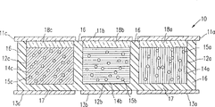
The element numbers explanation
10 miniature cup array components
11a, b, c battery lead plate
12a, b, c box
13a, b, c battery lead plate
14a, b, c dielectric solvent
15a, b, c pigment particle
16 sealed walls (wall of cup)
At the bottom of 17 miniature cups
18a, b, c seal cover
40 miniature cup arrays
41 miniature wall of cups
42 basal electrodes
43 substrate support nets
44 dielectric solvent components
45 charged pigment particles
46a thermoset precursors thing component
The 46b gland bonnet
47 conducting films
48 adhesive phases
50 miniature cup arrays
The 51a radiation curing material
The miniature wall of cup of 51b
The 51c unexposed area
52 conducting films
53 substrate support are online
54 darkened boxes (light tight district)
55 open regions (clear area)
56 photomasks
57 miniature cups
The 61a radiation curing material
The material that 61b solidifies
The material that 61c is uncured
62 conducting films
63 substrates
64 substrate conducting films
65 at interval
67 miniature cups
70 miniature cup arrays
The 71a radiation curing material
The material of the miniature wall of cup of 71b
72 substrate conducting films
73 substrate support nets
74 (conductors) district band
75 at interval
76 second photomasks
77 miniature cups
80 roll-to-roll photoetching process units
81 miniature cup arrays
82 photomasks
The 84a radiation curing material
The 84b polymeric material
86 substrate support nets
88 conducting film ITO districts band
90 driving/backing rolls
91 driving/backing rolls
92 photomasks are faced part directly
93 photomask flexure planes
100 driving/backing rolls
101 driving/backing rolls
103 supporting networks are faced part directly
104 storage/tensioning system
The output end of 105 roll-to-roll array manufacture craft production lines
105 ' storage/tensioning system
106 store or further processing
110 opacities
112 clear areas
114 fluorescence detectors
115 fluorescence detectors
120 partition walls
121 supporting networks
122 miniature cup boxes
First group of miniature cup array of 122a
Second group of miniature cup array of 122b
The 3rd group of miniature cup array of 122c
123 adhesive phases
124 positive photoresist layers
The 125a charged pigment is disperseed thing
125b pigment/solvent disperses thing
126a thermosetting sealing precursor
The 126b sealant
127 transparent top conductive films
128 precoating adhesive phases
130 roll-to-roll lithographic equipments
131 photoresist components
The 131a unexposed portion
The photoresist that 131b has exposed
132 photoresists store
133a, the b laminating roll
136 photomask endless belt
140 driving/backing rolls
141 driving/backing rolls
142 photomasks are faced directly
143 curvature portions
150 driven rollers
151 driven rollers
153 supporting networks are faced directly
160 clear areas
162 opaque zones
165 first miniature cup group faces
166 openings
202 supporting networks/ITO storage device
204 usefulness radiation curing precursors coating supporting network/ITO
206 by a miniature cup mask exposure
208 from miniature cup removal (washing) uncured radiation curing precursor
210 photoresist lamination storage devices
211 stacked photoresists
212 by first mask exposure
214 remove the photoresist that has exposed
216 usefulness, first pigment/solvent composition filling
218 sealings are also solidified first group of miniature cup
220 by second mask exposure
222 remove the (" photoresist that washing ") has exposed
224 usefulness, second pigment/solvent composition filling
226 sealings are also solidified second group of miniature cup
230 remove (" washing ") remaining photoresist
232 usefulness the 3rd pigment/solvent composition filling
234 sealings are also solidified the 3rd group of miniature cup
236 top ITO lamination storage devices
238 stacked top ITO
The 240 three look electrophoretic display device (EPD) miniature cup arrays that assemble

Claims (49)

1. method that is used to prepare a plurality of clear and definite definition structures, described method comprises the step that is not limited to following order:
(a) provide a supporting network;
(b) coating one deck radiation curing material on described supporting network;
(c) provide a photomask as a continuous loop, described continuous loop comprises the pattern of one of described at least structure of formal correspondence;
(d) with described photomask ring and described supporting network location, so that make at least a portion of described photomask ring and the substantially parallel orientation of at least a portion of described supporting network;
(e) with described photomask ring of moved further and described supporting network, so that described photomask ring of at least a portion and the described supporting network of at least a portion move abreast in same substantially direction;
(f) make radiation pass through a part of described photomask ring and directly arrive a part of described supporting network on described radiation curing material on, the substantially parallel orientation of described part of passing through described radiation of described a part of supporting network and described photomask ring, so that a part of graph exposure of described radiation curing material, and make another part of described radiation curing material keep unexposed; And
(g) remove described unexposed radiation curing material, to form a plurality of described clearly structures of definition.
2. method according to claim 1, wherein:
Described photomask ring and described supporting network are substantially with move fastly.
3. method that is used to prepare a plurality of miniature cups, described method comprises the step that is not limited to following order:
(a) provide a supporting network, described supporting network comprises a plurality of conduction region bands that are used for the described miniature cup of addressing;
(b) coating one deck radiation curing material on described supporting network;
(c) provide a kind of photomask as continuous loop, described photomask comprises the pattern of at least one miniature cup in the described miniature cup of formal correspondence;
(d) with described photomask ring of moved further and described supporting network;
(e) make radiation pass through a part of described photomask ring and directly arrive on the described radiation curing material on a part of described supporting network, the substantially parallel orientation of described part of passing through described radiation of described a part of supporting network and described photomask ring, so that a part of graph exposure of described radiation curing material, and make another part of described radiation curing material keep unexposed; And
(f) remove described unexposed radiation curing material, to form a plurality of described miniature cups.
4. method according to claim 3 also comprises with electrophoresis showed pigment/solvent composition or liquid crystal display component and fills described miniature cup and seal described miniature cup through filling.
5. method according to claim 4, wherein said filling step comprise with single electrophoresis showed pigment/solvent composition or liquid crystal display component fills all basically described miniature cups, so that form monochrome display.
6. method according to claim 4, wherein said filling step comprise with different electrophoresis showed pigment/solvent compositions or different liquid crystal display components fills described miniature cup, so that form multicolor display.
7. method that is used to prepare a plurality of clear and definite definition structures, described method comprise and being not limited to
The step of following order:
(a) provide a supporting network that comprises a plurality of elements;
(b) coating one deck radiation curing material on described supporting network;
(c) provide a photomask as a continuous loop, described continuous loop comprises the pattern with transparent region and zone of opacity;
(d) locate described photomask ring of at least a portion and the described supporting network of at least a portion in the mode of the described element on the corresponding described supporting network of described zone of opacity;
(e) to be synchronized with the movement to move described photomask ring and described supporting network, so that keep the predetermined spatial relationship between described photomask ring of at least a portion and the described supporting network of at least a portion, wherein said being synchronized with the movement is included in described photomask ring of the mobile abreast at least a portion of same substantially direction and the described supporting network of at least a portion;
(f) making radiation pass through a part of described photomask ring directly arrives on the radiation curing material on a part of described supporting network, the substantially parallel orientation of described part that the described radiation of described a part of supporting network and described photomask ring is passed through, so that the described transparent region by described photomask ring is to the described radiation curing material graph exposure of a part, and keep unexposed corresponding to the described radiation curing material of another part of the described zone of opacity of described photomask ring; And
(g) remove described unexposed radiation curing material, to form a plurality of described clear and definite definition structures.
8. method according to claim 7, wherein said photomask ring and described supporting network move with essentially identical speed.
9. method according to claim 8, wherein said photomask ring and described supporting network move with a constant speed.
10. method according to claim 7, wherein step (e) and step (f) are carried out simultaneously.
11. method according to claim 7, wherein step (b) is carried out continuously.
12. method according to claim 7, wherein step (e) is carried out continuously.
13. method according to claim 7, wherein step (f) is carried out continuously.
14. method according to claim 7 is further comprising the steps of:
(i) one of described element on the described supporting network of detection or a preformed mark;
(ii) detect one of described zone of opacity on the described photomask ring or a preformed mark; And
(iii) (ii) control the motion of described supporting network and described mask ring, so that at least a portion of at least a portion of described supporting network and described photomask forms predetermined spatial relationship in response to step (i) and step.
15. a method that is used to prepare a plurality of miniature cups, described method comprises the step that is not limited to following order:
(a) provide a supporting network, described supporting network comprises a plurality of conduction region bands that are used for the described miniature cup of addressing;
(b) coating one deck radiation curing material on described supporting network;
(c) provide a photomask as a continuous loop, described continuous loop comprises the pattern with transparent region and zone of opacity, and the wall construction of the formal corresponding described miniature cup of described transparent region;
(d) locate described photomask ring of at least a portion and the described supporting network of at least a portion in the mode of the described conduction region band on the corresponding described supporting network of described zone of opacity;
(e) to be synchronized with the movement to move described photomask ring and described supporting network, so that keep the predetermined spatial relationship between described photomask ring of at least a portion and the described supporting network of at least a portion;
(f) making radiation pass through a part of described photomask ring directly arrives on the radiation curing material on a part of described supporting network, the substantially parallel orientation of described part that the described radiation of described supporting network of a described part and described photomask ring is passed through, so that the described transparent region by described photomask ring is to the described radiation curing material graph exposure of a part, and keep unexposed corresponding to the described radiation curing material of another part of the described zone of opacity of described photomask ring; And
(g) remove described unexposed radiation curing material, to form described miniature cup.
16. method according to claim 15 is wherein removed the step of described unexposed radiation curing material and is carried out continuously.
17. method according to claim 3, wherein said conduction region band is transparent to visible light.
18. method according to claim 15, wherein said conduction region band is transparent to visible light.
19. a method that is used to prepare multicolor display, described method comprises:
(a) provide and answer a supporting network, described supporting network to comprise a plurality of open-topped preformed miniature cups that have;
(b) stacked one deck radiation curing material in the described open top of described miniature cup;
(c) provide first photomask as continuous loop, described continuous loop comprises the described open-topped pattern of formal corresponding first group of preliminary election miniature cup;
(d) with described photomask ring of moved further and described supporting network;
(e) make radiation pass through the described first photomask ring of a part, directly arrive on the radiation curing material in the open top that is layered in the described miniature cup on a part of described supporting network, the substantially parallel orientation of described part that the described radiation of described supporting network of a described part and the described first photomask ring is passed through, so that a part of graph exposure of described radiation curing material, and make another part of described radiation curing material keep unexposed;
(f) remove the radiation curing material of described exposure, so that the miniature cup of described first group of preliminary election is reopened mouth, and
(g) fill the described miniature cup of reopening first group of preliminary election of mouth with first electrophoresis showed pigment/solvent composition or liquid crystal display component.
20. method according to claim 19, wherein said radiation curing material are the photoresists of positivity effect.
21. method according to claim 19 also comprises the step that seals described first group of preliminary election miniature cup through filling.
22. method according to claim 21 is further comprising the steps of:
(i) provide second photomask as continuous loop, described continuous loop comprises the described open-topped pattern of formal corresponding second group of preliminary election miniature cup;
(ii) make radiation pass through the described second photomask ring of a part, directly arrive on the radiation curing material in the open top that is layered in the described miniature cup on a part of described supporting network, the substantially parallel orientation of described part that the described radiation of described supporting network of a described part and the described second photomask ring is passed through, so that a part of graph exposure of described radiation curing material, and make another part of described radiation curing material keep unexposed;
(iii) remove the radiation curing material of described exposure, so that the miniature cup of described second group of preliminary election is reopened mouth, and
(iv) fill the described miniature cup of reopening second group of preliminary election of mouth with second electrophoresis showed pigment/solvent composition or liquid crystal display component.
23. method according to claim 22 also comprises the step that seals described second group of preliminary election miniature cup through filling.
24. method according to claim 23 also comprises the steps:
(i) provide the 3rd photomask as continuous loop, described continuous loop comprises the described open-topped pattern of formal corresponding the 3rd group of preliminary election miniature cup;
(ii) make radiation pass through the described second photomask ring of a part, directly arrive on the radiation curing material in the open top of the described miniature cup that is layered in a part of described supporting network, the substantially parallel orientation of described part that the described radiation of described supporting network of a described part and described the 3rd photomask ring is passed through, so that a part of graph exposure of described radiation curing material, and make another part of described radiation curing material keep unexposed;
(iii) remove the radiation curing material of described exposure, so that the miniature cup of described the 3rd group of preliminary election is reopened mouth, and
(iv) fill the described miniature cup of reopening described the 3rd group of preliminary election of mouth with the 3rd electrophoresis showed pigment/solvent composition or liquid crystal display component.
25. method according to claim 24 also comprises the step that seals described the 3rd group of preliminary election miniature cup through filling.
26. method according to claim 25 also comprises first group, second group and the 3rd group of miniature cup coming stacked described sealing with a top laminate.
27. a method that is used to prepare multicolor display, described method comprises:
(a) provide a supporting network, described supporting network comprises a plurality of open-topped preformed miniature cups that have;
(b) photoresist of stacked one deck positivity effect in the described open top of described miniature cup;
(c) provide first photomask as a continuous loop, described continuous loop comprises the pattern with transparent region and zone of opacity, and the described open top of the miniature cup of corresponding first group of preliminary election in form of described transparent region;
(d) with described photomask ring of moved further and described supporting network;
(e) make radiation pass through the described first photomask ring of a part, directly arrive on the photoresist of the positivity effect in the open top that is layered in the described miniature cup on a part of described supporting network, the substantially parallel orientation of described part that the described radiation of described supporting network of a described part and the described first photomask ring is passed through, make the photoresist graph exposure of described positivity effect with described transparent region, and make photoresist keep unexposed corresponding to the positivity effect of the described zone of opacity of the described first photomask ring by the described first photomask ring;
(f) photoresist of the positivity effect of the described exposure of removal is reopened mouth with the miniature cup to described first group of preliminary election, and
(g) fill the described miniature cup of reopening described first group of preliminary election of mouth with first electrophoresis showed pigment/solvent composition or liquid crystal display component.
28. method according to claim 27 also comprises the step of the miniature cup of the described first group of preliminary election through filling of sealing.
29. method according to claim 28 is further comprising the steps of:
(i) provide second photomask as a continuous loop, described continuous loop comprises the pattern with transparent region and zone of opacity, and the described open top of the miniature cup of corresponding second group of preliminary election in form of described transparent region;
(ii) make radiation pass through the described second photomask ring of a part, directly arrive on the photoresist of the positivity effect in the open top that is layered in the described miniature cup on a part of described supporting network, the substantially parallel orientation of described part that the described radiation of described supporting network of a described part and the described second photomask ring is passed through, make the photoresist graph exposure of described positivity effect with described transparent region, and make photoresist keep unexposed corresponding to the positivity effect of the described zone of opacity of the described second photomask ring by the described second photomask ring;
(iii) remove the photoresist of the positivity effect of described exposure, so that the miniature cup of described second group of preliminary election is reopened mouth, and
(iv) fill the described described miniature cup of reopening second group of preliminary election of mouth of reopening mouth with second electrophoresis showed pigment/solvent composition or liquid crystal display component.
30. method according to claim 29 also comprises the step of the miniature cup of the described second group of preliminary election through filling of sealing.
31. method according to claim 30 is further comprising the steps of:
(i) provide the 3rd photomask as a continuous loop, described continuous loop comprises the pattern with transparent region and zone of opacity, and the described open top of the miniature cup of in form corresponding the 3rd group of preliminary election of described transparent region;
(ii) make radiation pass through described the 3rd photomask ring of a part, directly arrive on the photoresist of the positivity effect in the open top that is layered in the described miniature cup on a part of described supporting network, the substantially parallel orientation of described part that the described radiation of described supporting network of a described part and described the 3rd photomask ring is passed through, make the photoresist graph exposure of described positivity effect with described transparent region, and make photoresist keep unexposed corresponding to the positivity effect of the described zone of opacity of described the 3rd photomask ring by described the 3rd photomask ring;
(iii) remove the photoresist of the positivity effect of described exposure, so that the miniature cup of described the 3rd group of preliminary election is reopened mouth, and
(iv) fill the described miniature cup of reopening described the 3rd group of preliminary election of mouth with the 3rd electrophoresis showed pigment/solvent composition or liquid crystal display component.
32. method according to claim 31 also comprises the step of the miniature cup of described the 3rd group of preliminary election through filling of sealing.
33. device according to claim 32 further is included on first, second and the 3rd group of miniature cup of described sealing stacked one top laminate that is used for the described miniature cup of addressing.
34. method according to claim 33, wherein said top laminate is coated with bonding agent.
35. photoetching method, comprise by carrying out graph exposure with a synchronization-moving photomask of supporting network substrate that moves, wherein said supporting network substrate comprises polyethylene terephthalate, poly-naphthoic acid ethyl ester, or the tin indium oxide on the polycarbonate, described tin indium oxide is coated with radiation curing material, and described graph exposure is by making radiation pass through a part of described photomask, directly arrive and to realize on the described radiation curing material that is coated on the on-chip described tin indium oxide of described supporting network, the substantially parallel orientation of described part of described supporting network substrate and described photomask by radiation.
36. method according to claim 35, wherein said radiation curing material are the photoresists of positivity effect.
37. method according to claim 36, wherein said supporting network substrate is the tin indium oxide/polyethylene terephthalate that is coated with positive photoresist.
38. according to the described method of claim 37, wherein said positive photoresist develops after exposure, and described tin indium oxide/polyethylene terephthalate is through being etched with the discrete pattern of exposure.
39. according to the described method of claim 38, wherein said photoresist is strippable.
40. method according to claim 7, wherein said element are the conduction region bands.
41. one kind is used to prepare the clearly device of the structure of definition, described device comprises:
(a) supporting network driving mechanism engages supporting network with the described supporting network that leads movably, and wherein said supporting network is coated with one deck radiation curing material;
(b) photomask ring, described photomask ring comprise formal corresponding to the described clearly pattern of the structure of definition, are used for the optionally described radiation curing material of graph exposure;
(c) it is parallel-oriented with the described supporting network of at least a portion basically that photomask detent mechanism, described detent mechanism can make the part of described at least photomask ring orientate as;
(d) photomask driving mechanism is used for parallel in the same way basically at least a portion of described supporting network and at least a portion of described photomask endless belt of moving;
(e) be contained in radiation source to described photomask ring and described supporting network appropriate location; so that radiation is by the part of described photomask ring; directly arrive on the described radiation curing material on the part that is coated in described supporting network; the described part of described supporting network and the described part substantially parallel orientation of described photomask ring by radiation; be used for the optionally described radiation curing material of graph exposure, and
(f), be used to be coated with the solvent of the described unexposed portion of at least a removal near the solvent application mechanism of described supporting network installation.
42. according to the described device of claim 41, at least a portion of wherein said photomask ring and at least a portion of described supporting network are substantially with move fastly.
43. according to the described device of claim 41, the wherein said clearly structure of definition is a miniature cup, and
(a) described supporting network comprises a plurality of conduction region bands that are used for the described miniature cup of addressing;
(b) corresponding described miniature cup on the described pattern form of described photomask ring is used for directly and the selectivity figure is exposed to the described radiation curing material of a few part, and keeps that the described radiation curing material of another part is unexposed at least.
44. according to the described device of claim 43, wherein said conduction region band is transparent to visible light.
45. a device that is used to prepare multicolor display, described device comprises:
(a) supporting network driving mechanism engages supporting network with the described supporting network that leads movably, and wherein said supporting network comprises a plurality of preformed miniature cup disposed thereon, and each preformed miniature cup has an open top;
(b) one deck is arranged on the photoresist of the positivity effect on the described miniature cup, is used to seal described open top;
(c) a photomask ring, described photomask ring have in form the open-topped pattern corresponding to the miniature cup of first group of preliminary election, are used for the optionally photoresist of the described positivity effect of graph exposure;
(d) the photomask detent mechanism of installing near described supporting network, described detent mechanism is used for orientating the described supporting network of at least a portion as substantially parallel orientation with respect at least a portion of described photomask ring;
(e) photomask driving mechanism is used for parallel in the same way basically at least a portion of described supporting network and at least a portion of described photomask ring of moving;
(f) be contained in radiation source to described photomask ring and described supporting network appropriate location; so that radiation is by the part of described photomask ring; directly arrive and be arranged on the photoresist of the described positivity effect on the described miniature cup; described miniature cup is arranged on the part of described supporting network; the described part of described supporting network and the described part substantially parallel orientation of described photomask ring by radiation; be used for the optionally part of the photoresist of the described positivity effect of graph exposure; and keep another part at least of photoresist of described positivity effect unexposed, and
(g) the solvent application mechanism of installing near described supporting network is used to be coated with the solvent of the photoresist of at least a positivity effect that is used to remove described exposure, so that the open top of the miniature cup of described first group of preliminary election is reopened mouthful.
46., also comprise according to the described device of claim 45
(a) filling mechanism of installing near described supporting network is used for showing that with first component fills the miniature cup of first group of preliminary election reopening mouthful; And
(b) sealing mechanism of installing near described supporting network is in order to only to seal the miniature cup of first group of preliminary election through filling.
47. according to the described device of claim 46, also comprise the stacked mechanism of installing near described supporting network, in order to a stacked top laminate on the miniature cup of sealing, described top laminate comprises a plurality of conduction region bands that are used for the described miniature cup of addressing.
48. according to the described device of claim 47, wherein said conduction region band is transparent to visible light.
49. according to the described method of claim 46, wherein said first shows that component is electrophoresis showed component or liquid crystal display component.
CNB011396121A 2001-02-15 2001-11-23 Method for roll-to-roll display fabrication by simultaneous lithographic exposure on a substrate support web Expired - Fee Related CN1237387C (en)

Applications Claiming Priority (2)

Application Number Priority Date Filing Date Title
US09/784,972 US6933098B2 (en) 2000-01-11 2001-02-15 Process for roll-to-roll manufacture of a display by synchronized photolithographic exposure on a substrate web
US09/784,972 2001-02-15

Publications (2)

Publication Number Publication Date
CN1371023A CN1371023A (en) 2002-09-25
CN1237387C true CN1237387C (en) 2006-01-18

Family

ID=25134090

Family Applications (1)

Application Number Title Priority Date Filing Date
CNB011396121A Expired - Fee Related CN1237387C (en) 2001-02-15 2001-11-23 Method for roll-to-roll display fabrication by simultaneous lithographic exposure on a substrate support web

Country Status (10)

Country Link
US (1) US6906779B2 (en)
EP (1) EP1368710A2 (en)
JP (1) JP4298294B2 (en)
KR (1) KR100918600B1 (en)
CN (1) CN1237387C (en)
AU (1) AU2002244078A1 (en)
CA (1) CA2437411A1 (en)
MX (1) MXPA03007265A (en)
TW (1) TW556044B (en)
WO (1) WO2002065215A2 (en)

Cited By (1)

* Cited by examiner, † Cited by third party
Publication number Priority date Publication date Assignee Title
CN102834778A (en) * 2010-04-13 2012-12-19 株式会社尼康 Exposure apparatus, substrate processing apparatus, and device manufacturing method

Families Citing this family (116)

* Cited by examiner, † Cited by third party
Publication number Priority date Publication date Assignee Title
US6933098B2 (en) 2000-01-11 2005-08-23 Sipix Imaging Inc. Process for roll-to-roll manufacture of a display by synchronized photolithographic exposure on a substrate web
US7576904B2 (en) 2000-03-03 2009-08-18 Sipix Imaging, Inc. Electro-magnetophoresis display
US7142351B2 (en) 2000-03-03 2006-11-28 Sipix Imaging, Inc. Electro-magnetophoresis display
US6972893B2 (en) 2001-06-11 2005-12-06 Sipix Imaging, Inc. Process for imagewise opening and filling color display components and color displays manufactured thereof
US6795138B2 (en) 2001-01-11 2004-09-21 Sipix Imaging, Inc. Transmissive or reflective liquid crystal display and novel process for its manufacture
US8390918B2 (en) 2001-04-02 2013-03-05 E Ink Corporation Electrophoretic displays with controlled amounts of pigment
US7385751B2 (en) 2001-06-11 2008-06-10 Sipix Imaging, Inc. Process for imagewise opening and filling color display components and color displays manufactured thereof
US6788452B2 (en) 2001-06-11 2004-09-07 Sipix Imaging, Inc. Process for manufacture of improved color displays
JP4027178B2 (en) * 2001-09-12 2007-12-26 キヤノン株式会社 Electrophoretic display device
TWI229776B (en) 2002-01-03 2005-03-21 Sipix Imaging Inc A novel electrophoretic dispersion with a fluorinated solvent and a charge controlling agent
TWI250894B (en) * 2002-01-03 2006-03-11 Sipix Imaging Inc Functionalized halogenated polymers for microencapsulation
US7382514B2 (en) 2002-02-11 2008-06-03 Sipix Imaging, Inc. Core-shell particles for electrophoretic display
US6885146B2 (en) * 2002-03-14 2005-04-26 Semiconductor Energy Laboratory Co., Ltd. Display device comprising substrates, contrast medium and barrier layers between contrast medium and each of substrates
TW578121B (en) 2002-03-21 2004-03-01 Sipix Imaging Inc Magnetophoretic and electromagnetophoretic display
US7580180B2 (en) 2002-03-21 2009-08-25 Sipix Imaging, Inc. Magnetophoretic and electromagnetophoretic displays
US7113323B2 (en) 2002-03-21 2006-09-26 Sipix Imaging, Inc. Magnetophoretic and electromagnetophoretic displays
CN1209674C (en) 2002-04-23 2005-07-06 希毕克斯影像有限公司 Electromagnetic phoretic display
TW574538B (en) 2002-04-24 2004-02-01 Sipix Imaging Inc Compositions and processes for format flexible roll-to-roll manufacturing of electrophoretic displays
US7307778B2 (en) 2002-04-24 2007-12-11 Sipix Imaging, Inc. Compositions and processes for format-flexible, roll-to-roll manufacturing of electrophoretic displays
TWI310098B (en) 2002-05-03 2009-05-21 Sipix Imaging Inc Methods of surface modification for improving electrophoretic display performance
TWI329662B (en) 2002-05-17 2010-09-01 Sipix Imaging Inc Novel fluorinated silicon (iv) phthalocyanines and naphthalocyanines for electrophoretic, magnetophoretic or electromagnetophoretic display
TW583497B (en) 2002-05-29 2004-04-11 Sipix Imaging Inc Electrode and connecting designs for roll-to-roll format flexible display manufacturing
US7347957B2 (en) 2003-07-10 2008-03-25 Sipix Imaging, Inc. Methods and compositions for improved electrophoretic display performance
US8547628B2 (en) 2002-07-17 2013-10-01 Sipix Imaging, Inc. Methods and compositions for improved electrophoretic display performance
US7166182B2 (en) 2002-09-04 2007-01-23 Sipix Imaging, Inc. Adhesive and sealing layers for electrophoretic displays
TW575646B (en) * 2002-09-04 2004-02-11 Sipix Imaging Inc Novel adhesive and sealing layers for electrophoretic displays
US7616374B2 (en) 2002-09-23 2009-11-10 Sipix Imaging, Inc. Electrophoretic displays with improved high temperature performance
TWI327251B (en) * 2002-09-23 2010-07-11 Sipix Imaging Inc Electrophoretic displays with improved high temperature performance
TWI293715B (en) 2002-10-10 2008-02-21 Sipix Imaging Inc A method for inducing or enhancing the threshold of an electrophoretic display, an electrophoretic fluid and an electrophoretic display
JP2004145204A (en) * 2002-10-28 2004-05-20 Canon Inc Electrophoretic display element and method for producing the same
TWI297089B (en) 2002-11-25 2008-05-21 Sipix Imaging Inc A composition for the preparation of microcups used in a liquid crystal display, a liquid crystal display comprising two or more layers of microcup array and process for its manufacture
US9346987B2 (en) 2003-01-24 2016-05-24 E Ink California, Llc Adhesive and sealing layers for electrophoretic displays
US7572491B2 (en) 2003-01-24 2009-08-11 Sipix Imaging, Inc. Adhesive and sealing layers for electrophoretic displays
TWI228632B (en) * 2003-02-06 2005-03-01 Sipix Imaging Inc Improved electrophoretic display with a bi-modal particle system
JP4776532B2 (en) * 2003-05-02 2011-09-21 イー インク コーポレイション Electrophoresis display
GB2405217A (en) * 2003-08-22 2005-02-23 Qinetiq Ltd Phoretic display
US8257614B2 (en) 2003-11-04 2012-09-04 Sipix Imaging, Inc. Electrophoretic dispersions
US7277218B2 (en) 2003-11-04 2007-10-02 Sipix Imaging, Inc. Electrophoretic compositions
US7572394B2 (en) 2003-11-04 2009-08-11 Sipix Imaging, Inc. Electrophoretic dispersions
US8053171B2 (en) * 2004-01-16 2011-11-08 Semiconductor Energy Laboratory Co., Ltd. Substrate having film pattern and manufacturing method of the same, manufacturing method of semiconductor device, liquid crystal television, and EL television
US8535041B2 (en) * 2006-07-28 2013-09-17 Microcontinuum, Inc. Addressable flexible patterns
US9307648B2 (en) 2004-01-21 2016-04-05 Microcontinuum, Inc. Roll-to-roll patterning of transparent and metallic layers
KR100548937B1 (en) * 2004-02-02 2006-02-02 엘지전자 주식회사 Scan type exposure apparatus using film mask
US7504050B2 (en) 2004-02-23 2009-03-17 Sipix Imaging, Inc. Modification of electrical properties of display cells for improving electrophoretic display performance
JP2005292789A (en) * 2004-03-09 2005-10-20 Canon Inc Manufacturing method of display element
US20050253917A1 (en) * 2004-05-13 2005-11-17 Quanyuan Shang Method for forming color filters in flat panel displays by inkjetting
TWI283324B (en) * 2004-06-04 2007-07-01 Ind Tech Res Inst Method of liquid crystal alignment for a flexible liquid crystal display with microstructures
FR2879758B1 (en) * 2004-12-17 2007-04-27 Essilor Int METHOD FOR PRODUCING A TRANSPARENT OPTICAL ELEMENT, OPTICAL COMPONENT INVOLVED IN THIS METHOD AND OPTICAL ELEMENT THUS OBTAINED
FR2872589B1 (en) * 2004-07-02 2006-10-27 Essilor Int METHOD FOR PRODUCING A TRANSPARENT OPTICAL ELEMENT, OPTICAL COMPONENT INVOLVED IN THIS METHOD AND OPTICAL ELEMENT THUS OBTAINED
FR2872590B1 (en) 2004-07-02 2006-10-27 Essilor Int METHOD FOR PRODUCING AN OPHTHALMIC GLASS AND OPTICAL COMPONENT SUITABLE FOR CARRYING OUT SAID METHOD
KR101234173B1 (en) * 2004-07-02 2013-02-19 에씰로아 인터내셔날/콩파니에 제네랄 도프티크 Method for producing a transparent optical element, an optical component involved into said method and the thus obtained optical element
US7301693B2 (en) 2004-08-13 2007-11-27 Sipix Imaging, Inc. Direct drive display with a multi-layer backplane and process for its manufacture
FR2879757B1 (en) * 2004-12-17 2007-07-13 Essilor Int METHOD FOR PRODUCING A TRANSPARENT OPTICAL ELEMENT, OPTICAL COMPONENT INVOLVED IN THIS METHOD AND OPTICAL ELEMENT THUS OBTAINED
WO2006067650A1 (en) * 2004-12-20 2006-06-29 Koninklijke Philips Electronics N.V. Method of manufacturing an electrophoretic display device and electrophoretic display device
US8576162B2 (en) * 2005-03-14 2013-11-05 Sipix Imaging, Inc. Manufacturing processes of backplane for segment displays
US7460267B2 (en) 2005-07-15 2008-12-02 Applied Materials, Inc. Green printing ink for color filter applications
US7544723B2 (en) 2005-07-15 2009-06-09 Applied Materials, Inc. Blue printing ink for color filter applications
FR2888949B1 (en) * 2005-07-20 2007-10-12 Essilor Int PIXELLIZED OPTICAL COMPONENT WITH NANO PAROIS
FR2888954B1 (en) * 2005-07-20 2008-02-08 Essilor Int OPTICAL COMPONENT TRANSPORTS TO CELLS SEPARATED BY WALLS
FR2888947B1 (en) 2005-07-20 2007-10-12 Essilor Int OPTICAL CELL COMPONENT
FR2888951B1 (en) 2005-07-20 2008-02-08 Essilor Int RANDOMIZED PIXELLIZED OPTICAL COMPONENT, METHOD FOR MANUFACTURING THE SAME, AND USE THEREOF IN THE MANUFACTURE OF A TRANSPARENT OPTICAL ELEMENT
FR2888950B1 (en) 2005-07-20 2007-10-12 Essilor Int TRANSPARENT PIXELLIZED OPTICAL COMPONENT WITH ABSORBENT WALLS ITS MANUFACTURING METHOD AND USE IN FARICATION OF A TRANSPARENT OPTICAL ELEMENT
FR2888948B1 (en) 2005-07-20 2007-10-12 Essilor Int PIXELLIZED TRANSPARENT OPTIC COMPONENT COMPRISING AN ABSORBENT COATING, METHOD FOR PRODUCING THE SAME AND USE THEREOF IN AN OPTICAL ELEMENT
FR2888953B1 (en) * 2005-07-20 2008-02-08 Essilor Int PIXELLIZED OPTIC COMPONENT WITH APODIZED WALLS, METHOD FOR MANUFACTURING THE SAME AND USE THEREOF IN THE MANUFACTURE OF A TRANSPARENT OPTICAL ELEMENT
WO2007024134A1 (en) * 2005-08-26 2007-03-01 Fujifilm Manufacturing Europe B.V. Method and arrangement for generating and controlling a discharge plasma
US8441432B2 (en) 2005-09-23 2013-05-14 Sipix Imaging, Inc. Display cell structure and electrode protecting layer compositions
JP4938784B2 (en) 2005-10-26 2012-05-23 マイクロニック レーザー システムズ アクチボラゲット Writing apparatus and method
FR2897164B1 (en) 2006-02-09 2008-03-14 Commissariat Energie Atomique REALIZING CAVITIES THAT CAN BE FILLED BY A FLUID MATERIAL IN AN OPTICAL MICROTECHNOLOGICAL COMPOUND
US20070202442A1 (en) * 2006-02-24 2007-08-30 Eastman Kodak Company Method and apparatus for merging a mask and a printing plate
WO2007100849A2 (en) 2006-02-27 2007-09-07 Microcontinuum, Inc. Formation of pattern replicating tools
US20070268446A1 (en) * 2006-05-22 2007-11-22 Shie-Chang Jeng Liquid crystal device and method for forming the same
FR2907559B1 (en) * 2006-10-19 2009-02-13 Essilor Int ELECRO-COMMANDABLE OPTICAL COMPONENT COMPRISING A SET OF CELLS
US7905977B2 (en) * 2006-11-17 2011-03-15 Sipix Imaging, Inc. Post conversion methods for display devices
FR2910642B1 (en) * 2006-12-26 2009-03-06 Essilor Int TRANSPARENT OPTICAL COMPONENT WITH TWO CELL ARRAYS
FR2911404B1 (en) * 2007-01-17 2009-04-10 Essilor Int TRANSPARENT OPTICAL COMPONENT WITH CELLS FILLED WITH OPTICAL MATERIAL
US8940117B2 (en) 2007-02-27 2015-01-27 Microcontinuum, Inc. Methods and systems for forming flexible multilayer structures
WO2009096785A1 (en) * 2008-02-01 2009-08-06 Fujifilm Manufacturing Europe B.V. Method and apparatus for plasma surface treatment of a moving substrate
FR2929715B1 (en) 2008-04-04 2010-09-10 Commissariat Energie Atomique METHOD FOR PRODUCING MICRONIC OR SUBMICRONIC CAVITIES
FR2933205B1 (en) 2008-06-27 2010-08-13 Commissariat Energie Atomique IMPROVED METHOD FOR MAKING LIQUID-FILLED ENCLOSURES AND CLOSED BY A MEMBRANE
US8390781B2 (en) 2008-09-23 2013-03-05 Pinebrook Imaging Technology, Ltd. Optical imaging writer system
US8253923B1 (en) 2008-09-23 2012-08-28 Pinebrook Imaging Technology, Ltd. Optical imaging writer system
US8670106B2 (en) 2008-09-23 2014-03-11 Pinebrook Imaging, Inc. Optical imaging writer system
US8395752B2 (en) 2008-09-23 2013-03-12 Pinebrook Imaging Technology, Ltd. Optical imaging writer system
US8390786B2 (en) 2008-09-23 2013-03-05 Pinebrook Imaging Technology, Ltd. Optical imaging writer system
US8339573B2 (en) * 2009-05-27 2012-12-25 3M Innovative Properties Company Method and apparatus for photoimaging a substrate
US8436844B2 (en) * 2009-06-18 2013-05-07 Roche Diagnostics Operations, Inc. Bi-stable display fail safes and devices incorporating the same
KR101270699B1 (en) * 2010-06-22 2013-06-03 엘지디스플레이 주식회사 Apparatus for Manufacturing Liquid Crystal Diplay Panel
FR2963112B1 (en) 2010-07-21 2013-02-15 Commissariat Energie Atomique WALL MICROSTRUCTURE WITH DETERMINED OPTICAL PROPERTIES AND METHOD FOR PRODUCING MICROSTRUCTURES
KR101742125B1 (en) * 2010-09-30 2017-05-31 엘지디스플레이 주식회사 Method of fabrication electrophoretic display deivce
US8845912B2 (en) 2010-11-22 2014-09-30 Microcontinuum, Inc. Tools and methods for forming semi-transparent patterning masks
KR101347552B1 (en) * 2011-07-21 2014-01-10 주식회사 엘지화학 Mask and apparatus for manufacturing optical filter including the same
KR101924309B1 (en) 2011-12-20 2018-11-30 가부시키가이샤 니콘 Substrate processing device, device manufacturing system and device manufacturing method
TWI672258B (en) * 2012-05-18 2019-09-21 日商尼康股份有限公司 Exposure apparatus
US10401668B2 (en) 2012-05-30 2019-09-03 E Ink California, Llc Display device with visually-distinguishable watermark area and non-watermark area
US9388307B2 (en) * 2012-11-27 2016-07-12 E Ink California, Llc Microcup compositions
KR101957978B1 (en) * 2012-12-26 2019-03-14 엘지디스플레이 주식회사 Apparatus for Attaching Substrate of Display Device and Manufacturing Method using the same
US9589797B2 (en) 2013-05-17 2017-03-07 Microcontinuum, Inc. Tools and methods for producing nanoantenna electronic devices
TWI567996B (en) * 2014-02-18 2017-01-21 緯創資通股份有限公司 Crystal structure and manufacturing method thereof
WO2016060959A1 (en) 2014-10-17 2016-04-21 E Ink California, Llc Composition and process for sealing microcells
WO2017007607A1 (en) 2015-07-08 2017-01-12 3M Innovative Properties Company Photochromic articles containing a polyoxometalate and methods of making and using same
CN108351605B (en) * 2016-01-27 2020-12-15 株式会社Lg化学 Film mask, method for producing the same, pattern forming method using film mask, and pattern formed by film mask
KR102088385B1 (en) * 2016-04-20 2020-03-12 달리안 디케이이 엘씨디 컴패니, 리미티드 Subtractive mixed color electrophoretic display device and manufacturing method thereof
CN106061123A (en) * 2016-06-27 2016-10-26 太仓博轩信息科技有限公司 Keyboard thin film manufacturing technology
RU2710567C1 (en) * 2017-01-31 2019-12-27 Иллюмина, Инк. Devices for fluids and methods for making such devices
DE102017104886A1 (en) * 2017-03-08 2018-09-13 Osram Opto Semiconductors Gmbh Method for producing an optoelectronic component and optoelectronic component
US10802373B1 (en) 2017-06-26 2020-10-13 E Ink Corporation Reflective microcells for electrophoretic displays and methods of making the same
US10921676B2 (en) 2017-08-30 2021-02-16 E Ink Corporation Electrophoretic medium
US10698265B1 (en) 2017-10-06 2020-06-30 E Ink California, Llc Quantum dot film
RU178715U1 (en) * 2017-11-07 2018-04-17 Общество с ограниченной ответственностью "УРАЛМАТИК" Flexible decorative canvas with liquid crystals
TWI810685B (en) * 2017-11-24 2023-08-01 南韓商Lg化學股份有限公司 Method for producing substrate
KR102521144B1 (en) 2018-08-10 2023-04-12 이 잉크 캘리포니아 엘엘씨 Drive Waveforms for a Switchable Light Collimation Layer Containing a Bistable Electrophoretic Fluid
JP7108779B2 (en) 2018-08-10 2022-07-28 イー インク カリフォルニア, エルエルシー Switchable light collimating layer with reflector
US11397366B2 (en) 2018-08-10 2022-07-26 E Ink California, Llc Switchable light-collimating layer including bistable electrophoretic fluid
KR102827466B1 (en) * 2020-03-06 2025-07-02 삼성디스플레이 주식회사 Mask and method of manufacturing the same
WO2022178426A1 (en) * 2021-02-21 2022-08-25 The Regents Of The University Of California Roll-to-roll based 3d printing through computed axial lithography
JP2024536760A (en) 2021-09-16 2024-10-08 イー インク コーポレイション Switchable light collimating layer with improved transmission

Family Cites Families (55)

* Cited by examiner, † Cited by third party
Publication number Priority date Publication date Assignee Title
US3229607A (en) * 1963-03-19 1966-01-18 Polaroid Corp Photographic products, processes and apparatus
US3892568A (en) * 1969-04-23 1975-07-01 Matsushita Electric Industrial Co Ltd Electrophoretic image reproduction process
US3668106A (en) 1970-04-09 1972-06-06 Matsushita Electric Industrial Co Ltd Electrophoretic display device
US4093534A (en) 1974-02-12 1978-06-06 Plessey Handel Und Investments Ag Working fluids for electrophoretic image display devices
US4071430A (en) 1976-12-06 1978-01-31 North American Philips Corporation Electrophoretic image display having an improved switching time
US4285801A (en) 1979-09-20 1981-08-25 Xerox Corporation Electrophoretic display composition
JPS5934518A (en) 1982-08-21 1984-02-24 Matsushita Electric Ind Co Ltd electrophoresis panel
JPS60205452A (en) * 1984-03-30 1985-10-17 Canon Inc Exposing method
US4655897A (en) * 1984-11-13 1987-04-07 Copytele, Inc. Electrophoretic display panels and associated methods
JPH0652358B2 (en) 1985-10-28 1994-07-06 日本電信電話株式会社 Display device
US4680103A (en) 1986-01-24 1987-07-14 Epid. Inc. Positive particles in electrophoretic display device composition
JP2669609B2 (en) 1986-03-03 1997-10-29 旭化成工業株式会社 Liquid crystal display device
JP2612473B2 (en) 1988-05-28 1997-05-21 エヌオーケー株式会社 Electrophoretic display device and method of manufacturing the same
JP2733680B2 (en) 1989-02-25 1998-03-30 エヌオーケー株式会社 Electrophoretic display device and method of manufacturing the same
JP2777729B2 (en) 1989-04-26 1998-07-23 エヌオーケー株式会社 Electrophoretic display device and method of manufacturing the same
US5302235A (en) * 1989-05-01 1994-04-12 Copytele, Inc. Dual anode flat panel electrophoretic display apparatus
US5177476A (en) * 1989-11-24 1993-01-05 Copytele, Inc. Methods of fabricating dual anode, flat panel electrophoretic displays
JPH04113386A (en) 1990-08-31 1992-04-14 Hitachi Chem Co Ltd Electrophoresis display device
US5380362A (en) 1993-07-16 1995-01-10 Copytele, Inc. Suspension for use in electrophoretic image display systems
US5480938A (en) * 1993-11-22 1996-01-02 Xerox Corporation Low surface energy material
US5403518A (en) 1993-12-02 1995-04-04 Copytele, Inc. Formulations for improved electrophoretic display suspensions and related methods
EP0760872A4 (en) 1994-05-26 1997-12-10 Copytele Inc Fluorinated dielectric suspensions for electrophoretic image displays and related methods
US5745094A (en) * 1994-12-28 1998-04-28 International Business Machines Corporation Electrophoretic display
EP0830595A1 (en) * 1995-06-08 1998-03-25 Visible Genetics Inc. Microelectrophoresis chip for moving and separating nucleic acids and other charged molecules
US6124851A (en) 1995-07-20 2000-09-26 E Ink Corporation Electronic book with multiple page displays
US6017584A (en) 1995-07-20 2000-01-25 E Ink Corporation Multi-color electrophoretic displays and materials for making the same
US6120588A (en) * 1996-07-19 2000-09-19 E Ink Corporation Electronically addressable microencapsulated ink and display thereof
JP3358935B2 (en) 1995-10-02 2002-12-24 シャープ株式会社 Liquid crystal display device and method of manufacturing the same
KR100243190B1 (en) * 1996-06-10 2000-02-01 윤종용 Movable mirror device and manufacturing method thereof
US5930026A (en) 1996-10-25 1999-07-27 Massachusetts Institute Of Technology Nonemissive displays and piezoelectric power supplies therefor
GB2321718A (en) * 1997-01-31 1998-08-05 Nat Science Council LIquid crystal display
US5961804A (en) 1997-03-18 1999-10-05 Massachusetts Institute Of Technology Microencapsulated electrophoretic display
US5877848A (en) * 1997-04-02 1999-03-02 Macdermid Imaging Technology, Incorporated Continuous production of cross-linked resin relief images for printing plates
US5967871A (en) * 1997-07-24 1999-10-19 Photonics Systems, Inc. Method for making back glass substrate for plasma display panel
US6018383A (en) * 1997-08-20 2000-01-25 Anvik Corporation Very large area patterning system for flexible substrates
JP3654483B2 (en) * 1997-10-09 2005-06-02 富士写真フイルム株式会社 Manufacturing method of liquid crystal display device
US5914806A (en) 1998-02-11 1999-06-22 International Business Machines Corporation Stable electrophoretic particles for displays
AU3487599A (en) 1998-04-10 1999-11-01 E-Ink Corporation Full color reflective display with multichromatic sub-pixels
US6319381B1 (en) * 1998-06-11 2001-11-20 Micron Technology, Inc. Methods of forming a face plate assembly of a color display
JP2000035677A (en) * 1998-07-17 2000-02-02 Adtec Engineeng:Kk Aligner
JP2000075497A (en) * 1998-08-26 2000-03-14 Adtec Engineeng Co Ltd Aligner
JP2000155430A (en) * 1998-11-24 2000-06-06 Nsk Ltd Automatic alignment method for double-sided exposure equipment
JP2000241648A (en) * 1999-02-17 2000-09-08 Sony Corp Optical component manufacturing apparatus and method, and optical component
US6327072B1 (en) * 1999-04-06 2001-12-04 E Ink Corporation Microcell electrophoretic displays
US6524153B1 (en) * 1999-05-14 2003-02-25 Canon Kabushiki Kaisha Process for producing display device
JP2001056653A (en) 1999-06-11 2001-02-27 Ricoh Co Ltd Display liquid for electrophoretic display, display particles, and display medium, display device, display method, display card, recording sheet, display, reversible display signboard using them
DE19927359A1 (en) 1999-06-16 2000-12-21 Creavis Tech & Innovation Gmbh Electrophoretic displays made of light-scattering carrier materials
JP2001042118A (en) * 1999-08-02 2001-02-16 Canon Inc Color filter, continuous production method thereof, and liquid crystal element using the color filter
US6933098B2 (en) * 2000-01-11 2005-08-23 Sipix Imaging Inc. Process for roll-to-roll manufacture of a display by synchronized photolithographic exposure on a substrate web
US6930818B1 (en) 2000-03-03 2005-08-16 Sipix Imaging, Inc. Electrophoretic display and novel process for its manufacture
WO2001065309A2 (en) * 2000-03-02 2001-09-07 Chad Moore Reflective electro-optic fiber-based displays
US6545797B2 (en) * 2001-06-11 2003-04-08 Sipix Imaging, Inc. Process for imagewise opening and filling color display components and color displays manufactured thereof
US6750844B2 (en) * 2000-06-14 2004-06-15 Canon Kabushiki Kaisha Electrophoretic display device and process for production thereof
EP1195603B1 (en) 2000-10-04 2006-06-07 Seiko Epson Corporation Electrophoretic device and method of manufacturing it
US20020188053A1 (en) * 2001-06-04 2002-12-12 Sipix Imaging, Inc. Composition and process for the sealing of microcups in roll-to-roll display manufacturing

Cited By (1)

* Cited by examiner, † Cited by third party
Publication number Priority date Publication date Assignee Title
CN102834778A (en) * 2010-04-13 2012-12-19 株式会社尼康 Exposure apparatus, substrate processing apparatus, and device manufacturing method

Also Published As

Publication number Publication date
MXPA03007265A (en) 2004-06-30
CA2437411A1 (en) 2002-08-22
WO2002065215A8 (en) 2003-11-13
US20030152849A1 (en) 2003-08-14
AU2002244078A1 (en) 2002-08-28
WO2002065215A3 (en) 2003-10-09
CN1371023A (en) 2002-09-25
WO2002065215A2 (en) 2002-08-22
TW556044B (en) 2003-10-01
JP4298294B2 (en) 2009-07-15
JP2004525404A (en) 2004-08-19
US6906779B2 (en) 2005-06-14
KR20030091988A (en) 2003-12-03
EP1368710A2 (en) 2003-12-10
KR100918600B1 (en) 2009-09-25

Similar Documents

Publication Publication Date Title
CN1237387C (en) Method for roll-to-roll display fabrication by simultaneous lithographic exposure on a substrate support web
CN1295558C (en) Electrophoretic display with dual-mode switching
CN1275087C (en) Electrophoretic display with dual mode switching
CN1242300C (en) Electrophoretic display with dual-mode switching
CN1204448C (en) Improved back transmission electrophoresis display
CN1226664C (en) Improved electrophoretic display device and its manufacture
CN1289960C (en) Improved cataphoretic display device with double-mode shifting
CN1273860C (en) Improved electrophoresis display apparatus and its new manufacturing method
CN1109268C (en) Liquid crystal display flement substrate and liquid crystal display including the elements
CN1262875C (en) Improved electrophoretic display and novel process for its mfg.
CN101075068A (en) Electrophoresis display medium, component and method for using the same component to display image
CN101075066A (en) Electrophoresis display medium, component and method for using the same component to display image
CN101075067A (en) Electrophoresis display medium, component and method for using the same component to display image
CN101075057A (en) Electrophoresis display medium, component and method for using the same component to display image
CN101075062A (en) Electrophoresis display medium, component and method for using the same component to display image
CN101075061A (en) Electrophoresis display medium, component and method for using the same component to display image
US6885495B2 (en) Electrophoretic display with in-plane switching
CN1237140C (en) Composition and method for sealing microcups in roll-to-roll display manufacturing
CN101075064A (en) Electrophoresis display medium, component and method for using the same component to display image
CN101075058A (en) Electrophoresis display medium, component and method for using the same component to display image
CN1308763C (en) Microcapsule method and composition for electrophoretic display device
CN101075065A (en) Electrophoresis display medium, component and method for using the same component to display image
TW552485B (en) An improved electrophoretic display with in-plane switching
CN101075069A (en) Electrophoresis display medium, component and method for using the same component to display image
HK1048363A1 (en) Process for roll-to-roll manufacture of a display by synchronized photolithographic exposure on a substrate web

Legal Events

Date Code Title Description
C10 Entry into substantive examination
SE01 Entry into force of request for substantive examination
C06 Publication
PB01 Publication
C10 Entry into substantive examination
SE01 Entry into force of request for substantive examination
C14 Grant of patent or utility model
GR01 Patent grant
REG Reference to a national code

Ref country code: HK

Ref legal event code: WD

Ref document number: 1048363

Country of ref document: HK

CF01 Termination of patent right due to non-payment of annual fee

Granted publication date: 20060118

Termination date: 20141123

EXPY Termination of patent right or utility model