CN1299331C - Semiconductor device and manufacturing method thereof - Google Patents
Semiconductor device and manufacturing method thereof Download PDFInfo
- Publication number
- CN1299331C CN1299331C CNB011330945A CN01133094A CN1299331C CN 1299331 C CN1299331 C CN 1299331C CN B011330945 A CNB011330945 A CN B011330945A CN 01133094 A CN01133094 A CN 01133094A CN 1299331 C CN1299331 C CN 1299331C
- Authority
- CN
- China
- Prior art keywords
- film
- silicon
- tft
- hours
- nickel
- Prior art date
- Legal status (The legal status is an assumption and is not a legal conclusion. Google has not performed a legal analysis and makes no representation as to the accuracy of the status listed.)
- Expired - Lifetime
Links
Images












Classifications
-
- H—ELECTRICITY
- H10—SEMICONDUCTOR DEVICES; ELECTRIC SOLID-STATE DEVICES NOT OTHERWISE PROVIDED FOR
- H10P—GENERIC PROCESSES OR APPARATUS FOR THE MANUFACTURE OR TREATMENT OF DEVICES COVERED BY CLASS H10
- H10P14/00—Formation of materials, e.g. in the shape of layers or pillars
- H10P14/20—Formation of materials, e.g. in the shape of layers or pillars of semiconductor materials
- H10P14/38—Formation of materials, e.g. in the shape of layers or pillars of semiconductor materials characterised by treatments done after the formation of the materials
- H10P14/3802—Crystallisation or recrystallisation of non-monocrystalline semiconductor materials, e.g. regrowth
- H10P14/3806—Crystallisation or recrystallisation of non-monocrystalline semiconductor materials, e.g. regrowth using crystallisation-enhancing elements
-
- H—ELECTRICITY
- H10—SEMICONDUCTOR DEVICES; ELECTRIC SOLID-STATE DEVICES NOT OTHERWISE PROVIDED FOR
- H10D—INORGANIC ELECTRIC SEMICONDUCTOR DEVICES
- H10D30/00—Field-effect transistors [FET]
- H10D30/01—Manufacture or treatment
- H10D30/021—Manufacture or treatment of FETs having insulated gates [IGFET]
- H10D30/031—Manufacture or treatment of FETs having insulated gates [IGFET] of thin-film transistors [TFT]
- H10D30/0312—Manufacture or treatment of FETs having insulated gates [IGFET] of thin-film transistors [TFT] characterised by the gate electrodes
- H10D30/0314—Manufacture or treatment of FETs having insulated gates [IGFET] of thin-film transistors [TFT] characterised by the gate electrodes of lateral top-gate TFTs comprising only a single gate
-
- H—ELECTRICITY
- H10—SEMICONDUCTOR DEVICES; ELECTRIC SOLID-STATE DEVICES NOT OTHERWISE PROVIDED FOR
- H10D—INORGANIC ELECTRIC SEMICONDUCTOR DEVICES
- H10D30/00—Field-effect transistors [FET]
- H10D30/01—Manufacture or treatment
- H10D30/021—Manufacture or treatment of FETs having insulated gates [IGFET]
- H10D30/031—Manufacture or treatment of FETs having insulated gates [IGFET] of thin-film transistors [TFT]
- H10D30/0321—Manufacture or treatment of FETs having insulated gates [IGFET] of thin-film transistors [TFT] comprising silicon, e.g. amorphous silicon or polysilicon
-
- H—ELECTRICITY
- H10—SEMICONDUCTOR DEVICES; ELECTRIC SOLID-STATE DEVICES NOT OTHERWISE PROVIDED FOR
- H10D—INORGANIC ELECTRIC SEMICONDUCTOR DEVICES
- H10D86/00—Integrated devices formed in or on insulating or conducting substrates, e.g. formed in silicon-on-insulator [SOI] substrates or on stainless steel or glass substrates
- H10D86/01—Manufacture or treatment
- H10D86/021—Manufacture or treatment of multiple TFTs
- H10D86/0221—Manufacture or treatment of multiple TFTs comprising manufacture, treatment or patterning of TFT semiconductor bodies
- H10D86/0223—Manufacture or treatment of multiple TFTs comprising manufacture, treatment or patterning of TFT semiconductor bodies comprising crystallisation of amorphous, microcrystalline or polycrystalline semiconductor materials
- H10D86/0225—Manufacture or treatment of multiple TFTs comprising manufacture, treatment or patterning of TFT semiconductor bodies comprising crystallisation of amorphous, microcrystalline or polycrystalline semiconductor materials using crystallisation-promoting species, e.g. using a Ni catalyst
-
- H—ELECTRICITY
- H10—SEMICONDUCTOR DEVICES; ELECTRIC SOLID-STATE DEVICES NOT OTHERWISE PROVIDED FOR
- H10P—GENERIC PROCESSES OR APPARATUS FOR THE MANUFACTURE OR TREATMENT OF DEVICES COVERED BY CLASS H10
- H10P14/00—Formation of materials, e.g. in the shape of layers or pillars
- H10P14/20—Formation of materials, e.g. in the shape of layers or pillars of semiconductor materials
- H10P14/34—Deposited materials, e.g. layers
- H10P14/3402—Deposited materials, e.g. layers characterised by the chemical composition
- H10P14/3404—Deposited materials, e.g. layers characterised by the chemical composition being Group IVA materials
- H10P14/3411—Silicon, silicon germanium or germanium
-
- G—PHYSICS
- G09—EDUCATION; CRYPTOGRAPHY; DISPLAY; ADVERTISING; SEALS
- G09G—ARRANGEMENTS OR CIRCUITS FOR CONTROL OF INDICATING DEVICES USING STATIC MEANS TO PRESENT VARIABLE INFORMATION
- G09G2300/00—Aspects of the constitution of display devices
- G09G2300/04—Structural and physical details of display devices
- G09G2300/0404—Matrix technologies
- G09G2300/0408—Integration of the drivers onto the display substrate
Landscapes
- Thin Film Transistor (AREA)
- Recrystallisation Techniques (AREA)
Abstract
Description
本发明涉及一种制造集成电路的方法,或者更具体地涉及包括具有矩阵结构的矩阵器件(包括电——光显示器和半导体存储器)和作为开关元件的MOS或MIS(金属一绝缘体一半导体)型场效应元件(下文一般称之为MOS型元件)的半导体电路,其特征在于它的动态工作,诸如液晶显示和动态RAM(DRAM)及其驱动电路或类似图像传感器的集成驱动电路。本发明特别涉及一种采用薄膜半导体元件,诸如形成于绝缘表面的薄膜半导体晶体管或类似物,如MOS型元件的器件,还涉及具有薄膜晶体管的、其有源层是用晶体硅形成的器件。The present invention relates to a method of manufacturing integrated circuits, or more particularly to a matrix device comprising a matrix structure (including electro-optic displays and semiconductor memories) and MOS or MIS (metal-insulator-semiconductor) type A semiconductor circuit of a field effect element (hereinafter generally referred to as a MOS type element), characterized by its dynamic operation, such as a liquid crystal display and a dynamic RAM (DRAM) and its driving circuit or an integrated driving circuit like an image sensor. In particular, the present invention relates to a device using a thin film semiconductor element such as a thin film semiconductor transistor or the like formed on an insulating surface, such as a MOS type element, and to a device having a thin film transistor whose active layer is formed of crystalline silicon.
通常,用于薄膜器件,如薄膜绝缘栅型场效应晶体管(TFT)结晶硅半导体薄膜是用等离子CVD或热CVD方法形成的非晶硅膜在一种设备,如电炉中,在温度高于600℃经24小时以上进行结晶化的方法制备的。为了得到良好的特征,如高场迁移率和高可靠性,需要进行很多小时的热处理。Usually, for thin-film devices, such as thin-film insulated gate field-effect transistor (TFT) crystalline silicon semiconductor thin film is formed by plasma CVD or thermal CVD method of amorphous silicon film in a device, such as electric furnace, at a temperature higher than 600 It is prepared by crystallization for more than 24 hours at ℃. In order to obtain good characteristics, such as high field mobility and high reliability, many hours of heat treatment are required.
然而,通常的方法存在许多问题。问题之一是其生产率低,随之而来的是产品的成本变得高。例如,若花24小时作晶体化处理时,而若每片衬底花费2分钟时间处理,在相同的时间内,必须处理720片衬底。然而一个常用的管式炉一次最多能处理50片衬底,当仅用一个设备(反应管)时,每片花30分钟。即,为在2分钟处理1片,就必须用15个反应管。这意味着必须增加投资规模,那是因为投资被大幅度折旧,但不能在产品成本中反映出来。However, the usual method has many problems. One of the problems is that its productivity is low, with the result that the cost of the product becomes high. For example, if it takes 24 hours for the crystallization process, and if it takes 2 minutes for each substrate, 720 substrates must be processed in the same time. However, a commonly used tube furnace can process up to 50 substrates at a time, and each takes 30 minutes when only one device (reaction tube) is used. That is, 15 reaction tubes are required to process one tablet in 2 minutes. This means that the size of the investment must be increased because the investment is substantially depreciated but cannot be reflected in the cost of the product.
另一个问题在于热处理的温度。一般,用于制造TFT的衬底大致分为由纯氧化硅组成的玻璃,如石英玻璃、非碱硼硅酸玻璃,诸如Coning No 7059(下文称之为Coning 7059)。在这些衬底中,前者就温度而言不成问题,因为它的耐热性好,因而能按与正常半导体集成电路的片子加工工艺相同的方式来操作,然而,它的成本高,并随衬底面积的增大而指数增加。所以,它仅被用作面积比较小的TFT集成电路。Another problem is the temperature of the heat treatment. In general, substrates used for manufacturing TFTs are roughly classified into glasses composed of pure silicon oxide, such as quartz glass, and non-alkali borosilicate glass, such as Coning No. 7059 (hereinafter referred to as Coning 7059). Among these substrates, the former is not a problem in terms of temperature, because of its good heat resistance, it can be operated in the same way as normal semiconductor integrated circuit chip processing, however, its cost is high, and it is not compatible with the substrate. increases exponentially with increasing base area. Therefore, it is only used as a TFT integrated circuit with a relatively small area.
另一方面,与石英玻璃相比,非碱玻璃的成本虽然十分低,但在耐热方面还存在问题。因为它的应变点一般在550~650℃,对某些易于应用的材料,或低于600℃。当用600℃做热处理时,就会导致衬底出现不可逆的收缩或翘曲之类的问题。当衬底的对角线距离超过10cm时尤为显著。基于上述原因,人门认为必须保持热处理条件低于550℃,时间不超过4小时,以便降低硅半导体膜结晶化的成本。因而,本发明的一个目的是提供一种半导体的制造方法,其排除这些条件,以及采用这种半导体来制造半导体器件的方法。On the other hand, although the cost of non-alkali glass is very low compared with quartz glass, there is still a problem in terms of heat resistance. Because its strain point is generally 550-650°C, or lower than 600°C for some materials that are easy to apply. When heat treatment is performed at 600°C, problems such as irreversible shrinkage or warpage of the substrate will result. Especially when the diagonal distance of the substrate exceeds 10cm. Based on the above reasons, people believe that it is necessary to keep the heat treatment conditions below 550°C for no more than 4 hours in order to reduce the cost of crystallization of the silicon semiconductor film. Accordingly, an object of the present invention is to provide a method of manufacturing a semiconductor which eliminates these conditions, and a method of manufacturing a semiconductor device using the semiconductor.
近来。已进行有关具有薄膜有源层(或称为有源区)的绝缘栅型半导体器件的研究。特别是对薄膜绝缘栅晶体管或所谓的薄膜晶体管(TFT)做了热烈的研究。它们形成在透明的绝缘衬底上,用来控制每个图象和驱动它的在显示器件,如一个具有矩阵结构的液晶显示器中的矩阵,或用作一个同样形成于绝缘衬底上的图象传感器的驱动电路。根据所用的半导体的材料的晶体状态,它们被分成非晶硅TFT或结晶硅(或称多晶硅)TFT。recently. Research has been conducted on an insulated gate type semiconductor device having a thin-film active layer (or referred to as an active region). In particular thin-film insulated-gate transistors or so-called thin-film transistors (TFTs) have been intensively studied. They are formed on a transparent insulating substrate and are used to control each image and drive it in a display device, such as a matrix in a liquid crystal display with a matrix structure, or as a pattern also formed on an insulating substrate. Like the drive circuit of the sensor. They are classified into amorphous silicon TFTs or crystalline silicon (or polysilicon) TFTs according to the crystal state of the material of the semiconductor used.
最近,正开展利用介于多晶和非晶硅之间的中间态的材料的研究。虽然中间态尚处于讨论中,但所有那些用任何热处理(如用强能量,象激光辐照,在450℃以上的温度的退火)获得的某些晶体状态,在本说明书中被称为结晶硅。Recently, research into materials utilizing an intermediate state between polycrystalline and amorphous silicon is being conducted. Although intermediate states are still under discussion, all those certain crystalline states obtained by any thermal treatment (such as annealing with intense energy, like laser irradiation, at temperatures above 450°C), are referred to in this specification as crystalline silicon .
结晶硅TFT作为一个所谓的SOI技术远被用于单晶硅集成电路中,在高集成的SRAM中它被用作一个负载晶体管。然而,在这种情况下,很少用非晶硅TFT。Crystalline silicon TFT is used as a so-called SOI technology in monocrystalline silicon integrated circuits, and it is used as a load transistor in highly integrated SRAM. In this case, however, amorphous silicon TFTs are rarely used.
还有绝缘衬底上的半导体电路的工作速度可以很高,因为在衬底和布线之间没有电容耦合,因而提出一种技术,用它作很高速度的微处理机或很高速度的存储器。In addition, the operating speed of the semiconductor circuit on the insulating substrate can be very high, because there is no capacitive coupling between the substrate and the wiring, so a technology is proposed to use it as a very high-speed microprocessor or a very high-speed memory .
一般,一个处于非晶态的半导体的场迁移率是低的,因而不能用于工作速度要求很高的TFT。还有,因为P型非晶硅的场迁移率显著的小,不能制成P-型TFT(PMOS的TFT),因而,不能与N沟型TFT(NMOS的TFT)结合形成一个互补MOS电路(CMOS)。Generally, the field mobility of a semiconductor in an amorphous state is low, and thus cannot be used for TFTs requiring a high operating speed. Also, because the field mobility of P-type amorphous silicon is significantly small, it cannot be made into a P-type TFT (PMOS TFT), therefore, it cannot be combined with an N-channel TFT (NMOS TFT) to form a complementary MOS circuit ( CMOS).
然而,用非晶半导体形成的TFT有一个优点,OFF(关断)电流小。因而它可被用于:工作速度要求不是很高、仅一种导电类型即可、以及要求一个电荷保持能力高的TFT,如具有小矩阵规模的液晶显示的有源矩阵电路的晶体管。然而,将非晶硅TFT用于尖端应用,如具有大规模矩陈的液晶显示器中,是困难的。还有它自然不能用于显示的外围电路和要求工作速度高的图象传感器的驱动电路。However, a TFT formed of an amorphous semiconductor has an advantage that an OFF (turn-off) current is small. Therefore, it can be used in a TFT requiring not very high operating speed, only one conductivity type, and requiring a high charge retention capability, such as a transistor of an active matrix circuit of a liquid crystal display with a small matrix scale. However, it is difficult to use amorphous silicon TFTs for cutting-edge applications such as liquid crystal displays with large-scale matrix. Also, it cannot naturally be used in peripheral circuits for display and drive circuits for image sensors requiring high operating speeds.
另一方面,结晶半导体的场迁移率大于非晶体半导体的迁移率,可以高速工作。例如,在由激光退火利用再结晶的硅膜制得的TFT中,得到地场迁移率有300cm2/v·s之大。由在正常单晶硅衬底上形成的MOS晶·体管的场迁移率大约是500cm2/v·s来看,上面的迁移率则是一个极大的数值。但是,单晶硅上的MOS电路的工作速度受衬底与布线间的寄生电容所限,对用结晶化的硅膜制成的TFT来说,则没有这种限制,因为它是形成于绝缘衬底上的。所以在这种TFT中,可达到预期显著高的工作速度。On the other hand, crystalline semiconductors have higher field mobility than amorphous semiconductors and can operate at high speeds. For example, in a TFT produced by laser annealing using a recrystallized silicon film, a field mobility as large as 300 cm 2 /v·s was obtained. Considering that the field mobility of a MOS transistor formed on a normal single crystal silicon substrate is about 500 cm 2 /v·s, the above mobility is an extremely large value. However, the operating speed of MOS circuits on single crystal silicon is limited by the parasitic capacitance between the substrate and wiring. For TFTs made of crystallized silicon films, there is no such limitation because they are formed on insulating on the substrate. Therefore, in such a TFT, a remarkably high operating speed can be expected.
另外,因为不仅能得到NMOS TFT。而且同样还能得到PMOSTFT,所以可以用结晶硅形成CMOS电路。例如,在有源矩阵系统的液晶显示器中,已知用CMOS结晶硅TFT可构成一个不仅具有有源矩阵部分。而且还有外围电路(如驱动器)的所谓的单片结构的系统。用于前述的SRAM的TFT正是所提示的这一点,其中的PMOS作为负载晶体管是由TFT构成的。In addition, because not only NMOS TFT can be obtained. Moreover, PMOSTFT can also be obtained in the same way, so CMOS circuits can be formed with crystalline silicon. For example, in a liquid crystal display of an active matrix system, it is known that a CMOS crystalline silicon TFT can be constructed not only with an active matrix portion. There are also so-called monolithically structured systems of peripheral circuits such as drivers. The TFTs used for the aforementioned SRAM are just that suggested, where the PMOS as a load transistor is made of TFTs.
再有,用于单晶IC技术的自对准工艺,在正常非晶TFT中不易形成源/漏区,并且由栅极与源/漏区的几何重叠引起的寄生电容带来一个问题。但结晶硅TFT有显著压低这种寄生电容的优点。因为它可采用自对准工艺。Furthermore, the self-aligned process used in single crystal IC technology, it is not easy to form source/drain regions in normal amorphous TFT, and the parasitic capacitance caused by the geometric overlap of gate and source/drain regions poses a problem. But crystalline silicon TFTs have the advantage of significantly reducing this parasitic capacitance. Because it can use self-alignment process.
然而,当没有电压施加于栅极(非选时期)时,结晶硅TFT的漏电流,与非晶硅TFT的漏电流相比,是大的。但采取这样一种对策,提供一个辅助电容去补偿漏电流,并将两个TFT串联连接,减少它用于液晶显示时的漏电流。However, when no voltage is applied to the gate (non-selection period), the leakage current of the crystalline silicon TFT is large compared with that of the amorphous silicon TFT. But to take such a countermeasure, provide an auxiliary capacitor to compensate the leakage current, and connect two TFTs in series to reduce the leakage current when it is used for liquid crystal display.
例如,已经提出:先形成一非晶硅,再在其上选择地辐照激光,仅仅使外围电路结晶化的方法,以便在同一衬底上形成具有高迁移率的单片多晶硅TFT的外围电路,同时利用非晶硅TFT的高截止(OFF)阻抗。For example, it has been proposed to form an amorphous silicon first, and then selectively irradiate laser light on it to crystallize only the peripheral circuit, so as to form the peripheral circuit of a monolithic polysilicon TFT with high mobility on the same substrate. , while using the high cut-off (OFF) resistance of amorphous silicon TFT.
然而,目前其产量还是低的,那是因为激光辐照工艺的可靠性尚有问题(如在辐照表面内辐照能量的均匀度不好),因而终于采用一种用非晶硅TFT构成一个矩阵。再按TAB或类似方法连接单晶集成电路构成驱动电路的方法。然而,从连接的结构限制考虑,本方法要宽于0.1mm的象素间距,并且其成本也变得很高。However, its output is still low at present, that is because there are still problems in the reliability of the laser irradiation process (such as poor uniformity of irradiation energy in the irradiated surface), so a kind of amorphous silicon TFT is finally adopted. a matrix. Then press TAB or a similar method to connect a single crystal integrated circuit to form a driving circuit. However, this method is wider than the pixel pitch of 0.1mm in view of the structural constraints of the connection, and its cost also becomes high.
本发明想要解决这些难题,但不希望使工艺复杂化,最后降低成本率,提高成本。本发明想要容易地、区别对待地制造两种类型的TFT,即一种要求迁移率高的TFF和一种要求漏电流低的TFT,同时保持批量生产,并尽量减少工艺的改动。The present invention intends to solve these difficult problems, but does not wish to complicate the process, and finally reduce the cost rate and increase the cost. The present invention intends to easily and discriminately manufacture two types of TFTs, a TFT requiring high mobility and a TFT requiring low leakage current, while maintaining mass production and minimizing process changes.
另外,本发明的另一个目的在于减小CMOS电路中NMOS和PMOS迁移率的差值。NMOS和PMOS间差值的减小可增加电路设计的自由度。In addition, another object of the present invention is to reduce the difference in mobility between NMOS and PMOS in a CMOS circuit. The reduction of the difference between NMOS and PMOS increases the degree of freedom in circuit design.
采用本发明的半导体电路不是万能的。即,本发明适合于利用电场作用改变透光率或反光率的那种材料,将材料夹在面对面的两电极间,并在电极间施加电场来显示图象的有源矩阵电路,如液晶显示器;在电容内存贮电荷用于保持记忆的存储器件,如DRAM:具有动态电路的电路,如动态移位寄存器,它用MOS晶体管的MOS结构部位的电容或其它电容驱动下一个电路:以及具有数字电路和控制模拟信号输出的电路,如图象传感器的驱动电路。本发明特别适合于动态电路和静态电路混合设置的一种电路。A semiconductor circuit employing the present invention is not omnipotent. That is, the present invention is suitable for utilizing the electric field effect to change that kind of material of light transmittance or light reflectance, the material is sandwiched between two facing electrodes, and the active matrix circuit that applies electric field to display image between electrodes, as liquid crystal display ; Storage devices that store charges in capacitors for memory retention, such as DRAM: circuits with dynamic circuits, such as dynamic shift registers, which drive the next circuit with the capacitance of the MOS structure of the MOS transistor or other capacitances: and with Digital circuits and circuits that control analog signal output, such as drive circuits for image sensors. The invention is particularly suitable for a circuit in which dynamic circuits and static circuits are mixed.
本发明的特征在于:先在硅膜之上或之下形成含有由下列材料所组成的组中选出的一种材料的岛状膜、圆点、颗粒、团块或线条,再使其在低于仅仅一般非晶硅热处理过程中的结晶化温度做较短时间的退火,即可得到结晶硅膜,这些材料如下:镍、铁、钴、钌、铑、钯、锇、铱、铂、钪、钛、钒、铬、锰、铜、锌、金和银,以及它们的组合物,而硅膜处于非晶态或无序晶态(例如,一种结晶好的部分和非晶部分相混的状态),可以说基本上是处于非晶态。退火可以在氢、氧或氮气氛下进行。退火可以按下列条件进行:(1)在含氧的气氛中加热A小时,然后在含氢的气氛中加热B小时;(2)在含氧的气氛中加热C小时,再在含氮的气氛中加热D小时;(3)在含氢的气氛中加热E小时,再在含氧的气氛中加热F小时;(4)在含氢的气氛中加热G小时,再在含氮的气氛中加热H小时;(5)在含氮的气氛中加热I小时,再在含氧的气氛中加热J小时:(6)在含氮的气氛中加热K小时,再在含氢的气氛中加热L小时;(7)在含氧的气氛中加热M小时,在含氢的气氛中加热N小时,然后在含氮的气氛中加热P小时;(8)在含氧的气氛中加热Q小时、在含氮的气氛中加热R小时,再在含氢的气氛中加热S小时;(9)在含氢的气氛中加热T小时,在氧气氛中加热U小时,再在含氮的气氛中加热V小时;(10)在含氢的气氛中加热W小时,在含氮的气氛中加热X小时,再在含氧的气氛中加热Y小时;(11)在含氮的气氛中加热Z小时,在含氧的气氛中加热A′小时。再在含氢的气氛中加热B′小时;或(12)在含氮的气氛中加热C′小时,在含氢的气氛中加热D′小时,再在含氧的气氛中加热E′小时。The present invention is characterized in that an island-shaped film, dots, particles, agglomerates or lines containing a material selected from the group consisting of the following materials are first formed on or under the silicon film, and then placed on the silicon film The crystalline silicon film can be obtained by annealing for a shorter time than the crystallization temperature in the heat treatment process of general amorphous silicon. These materials are as follows: nickel, iron, cobalt, ruthenium, rhodium, palladium, osmium, iridium, platinum, Scandium, titanium, vanadium, chromium, manganese, copper, zinc, gold, and silver, and combinations thereof, while silicon films are in an amorphous or disordered crystalline state (e.g., a well-crystallized partial and amorphous partial phase Mixed state), it can be said that it is basically in an amorphous state. Annealing can be performed under a hydrogen, oxygen or nitrogen atmosphere. Annealing can be carried out according to the following conditions: (1) heating in an atmosphere containing oxygen for A hours, then heating in an atmosphere containing hydrogen for B hours; (2) heating in an atmosphere containing oxygen for C hours, and then heating in an atmosphere containing nitrogen (3) heating in an atmosphere containing hydrogen for E hours, and then heating in an atmosphere containing oxygen for F hours; (4) heating in an atmosphere containing hydrogen for G hours, and then heating in an atmosphere containing nitrogen H hours; (5) heating in a nitrogen-containing atmosphere for 1 hour, then heating in an oxygen-containing atmosphere for J hours: (6) heating in a nitrogen-containing atmosphere for K hours, and then heating in a hydrogen-containing atmosphere for L hours (7) heating in an oxygen-containing atmosphere for M hours, heating in a hydrogen-containing atmosphere for N hours, and then heating in a nitrogen-containing atmosphere for P hours; (8) heating in an oxygen-containing atmosphere for Q hours, in an atmosphere containing Heating in an atmosphere of nitrogen for R hours, and then heating in an atmosphere containing hydrogen for S hours; (9) heating in an atmosphere containing hydrogen for T hours, heating in an atmosphere of oxygen for U hours, and then heating in an atmosphere containing nitrogen for V hours (10) heating W hours in an atmosphere containing hydrogen, heating X hours in an atmosphere containing nitrogen, and heating Y hours in an atmosphere containing oxygen; (11) heating Z hours in an atmosphere containing nitrogen, and heating in an atmosphere containing nitrogen Heat A' in an oxygen atmosphere for 1 hour. Then heat in an atmosphere containing hydrogen for B' hours; or (12) heat in an atmosphere containing nitrogen for C' hours, heat in an atmosphere containing hydrogen for D' hours, and then heat in an atmosphere containing oxygen for E' hours.
关于硅膜的结晶化,过去已经提出一种先形成作为晶核或籽晶的结晶的岛状膜,再使它固相外延生长(例如日本特开平1-214110)的方法。然而,在600℃的温度下,用此方法,可勉强生长晶体。一般,当硅从非晶态转变为结晶态时,它经受一个工艺过程,非晶态分子链被分开,并在把分开的分子置于不与其它分子耦连的状态之后,分子与某些结晶化的分子相结合,而再结合成为晶体的一部分。然而分离原始分子链并保持它们不与其它分子耦合的状态的能量,在此工艺过程中是大的,它阻止了结晶化反应。为提供此能量,用1000℃的温度,需用数分钟,或用600℃的温度,需用数十小时。因为,时间与温度(=能量)有指数关系,例如,在低于600℃或在550℃,几乎一点看不到结晶化反应的进展。固相外延结晶化的概念对此问题也不能给予任何解答。Regarding the crystallization of a silicon film, there has been proposed a method of forming a crystalline island-like film as a nucleus or a seed crystal and then growing it by solid phase epitaxy (for example, Japanese Patent Application Laid-Open No. 1-214110). However, at a temperature of 600°C, crystals could barely grow by this method. Generally, when silicon changes from an amorphous state to a crystalline state, it undergoes a process in which the amorphous molecular chains are separated, and after placing the separated molecules in a state where they are not coupled to other molecules, the molecules are bonded to some The crystallized molecules combine and recombine to become part of the crystal. However, the energy to separate the original molecular chains and keep them uncoupled from other molecules is large during this process, which prevents the crystallization reaction. To provide this energy, it takes several minutes at a temperature of 1000°C, or tens of hours at a temperature of 600°C. Because time has an exponential relationship with temperature (=energy), for example, at less than 600°C or at 550°C, progress of the crystallization reaction is hardly seen at all. The concept of solid-phase epitaxy crystallization cannot give any answer to this question.
本发明的发明者考虑到,用某些催化作用来降低前述工艺过程中的阻止能量,它完全不同于常规的固相结晶化概念。本发明者提到:镍(Ni)、铁(Fe)、钴(Co)、钌(Ru)、铑(Rh)、钯(Pd)、锇(Os)、铱(Ir)、铂(Pt)、钪(Sc)、钛(Ti)、钒(V)、铬(Cr)、锰(Mn)、铜(Cu)、锌(Zn)、金(Au)以及银(Ag),易于与硅耦连。The inventors of the present invention considered that some catalysis is used to reduce the stopping energy in the aforementioned process, which is completely different from the conventional concept of solid phase crystallization. The inventor mentioned: nickel (Ni), iron (Fe), cobalt (Co), ruthenium (Ru), rhodium (Rh), palladium (Pd), osmium (Os), iridium (Ir), platinum (Pt) , scandium (Sc), titanium (Ti), vanadium (V), chromium (Cr), manganese (Mn), copper (Cu), zinc (Zn), gold (Au) and silver (Ag), easy to couple with silicon even.
例如,本发明者指出,就镍来说,它易于制成硅化镍(NiSix,0.4≤X≤2.5)其晶格常数接近硅晶体的晶格常数。那么,当模拟三元系-晶体硅·硅化镍·非晶硅中的能量和其它条件时,可以观察到,在与硅化镍的边界上,非晶硅易于反应,并大约发生下列反应:For example, the present inventors pointed out that, in the case of nickel, it is easy to make nickel silicide (NiSix, 0.4≤X≤2.5) whose lattice constant is close to that of silicon crystal. Then, when simulating the energy and other conditions in the ternary system - crystalline silicon · nickel silicide · amorphous silicon, it can be observed that on the boundary with nickel silicide, amorphous silicon is easy to react, and approximately the following reactions occur:
(硅A和硅B指示硅的位置)(Silicon A and Silicon B indicate the location of the silicon)
阻止此反应的势能是非常低的,反应温度也是低的。此反应式指明,在非晶硅被镍转变为晶体硅时,进行该反应。可以发现,此反应实际上起始于580℃以下,即使在450℃也能观察到此反应。当然,温度越高,反应进展的速度越快。用上述的其它金属元素,也能看到相同的作用。The potential energy to prevent this reaction is very low, as is the reaction temperature. This reaction formula indicates that the reaction proceeds when amorphous silicon is converted to crystalline silicon by nickel. It was found that the reaction actually started below 580°C and was observed even at 450°C. Of course, the higher the temperature, the faster the reaction progresses. The same effect can also be seen with the other metal elements mentioned above.
根据本发明,先形成一个至少含有Ni、Fe、Co、Ru、Rh、Pd、Os、Ir、Pt、Sc、Ti、V、Cr、Mn、Cu、Zn、Au以及Ag之中的一种元素的膜、颗粒或团块,如岛状、条状、线状、点状或膜状的镍或上述其它单纯金属衬底或它们的硅化物,用作起始点,再按上述反应,把那些金属元素从点扩展到四周,使晶体硅区域延展。另外,氧化物不适于作含有那些金属元素的材料,因为氧化物是一种稳定化合物,不能启动前述反应。According to the present invention, first form an element containing at least one of Ni, Fe, Co, Ru, Rh, Pd, Os, Ir, Pt, Sc, Ti, V, Cr, Mn, Cu, Zn, Au and Ag Films, particles or agglomerates, such as islands, strips, lines, dots or films of nickel or other simple metal substrates mentioned above or their silicides, are used as starting points, and then according to the above reaction, those The metallic elements spread from the point to the perimeter, extending the crystalline silicon region. In addition, oxides are not suitable as materials containing those metal elements because oxides are stable compounds that cannot initiate the aforementioned reactions.
从一特定点延展的晶体硅的结构,虽然不同于常规固相外延生长,但它接近于单晶硅,结晶的连续性好,因而适宜用作半导体器件,如TFT。然而,当包括加速结晶化的前述金属如镍等材料被均匀设置于衬底上时,会出现无数个结晶化的起始点,因此难以得到结晶性良好的膜。The structure of crystalline silicon extending from a specific point is different from conventional solid-phase epitaxy, but it is close to single crystal silicon, and the continuity of crystallization is good, so it is suitable for semiconductor devices such as TFT. However, when a material including the aforementioned metal that accelerates crystallization such as nickel is uniformly provided on a substrate, countless starting points of crystallization occur, so it is difficult to obtain a film with good crystallinity.
当氢在作为结晶化起始材料的非晶硅中的浓度更低些,所得到的结果更好些。然而,因为当结晶进展时,会释放出氢,故没有看出在所得到的硅膜内的氢浓度和作为起始材料的非晶硅中的氢浓度之间的清楚的相互关系。本发明的晶体硅中的氢浓度一般高于0.001at%,低于5at%。Better results were obtained when the concentration of hydrogen in the amorphous silicon as the starting material for crystallization was lower. However, since hydrogen is released as crystallization progresses, no clear correlation is seen between the hydrogen concentration in the resulting silicon film and the hydrogen concentration in amorphous silicon as a starting material. The hydrogen concentration in the crystalline silicon of the present invention is generally higher than 0.001 at%, lower than 5 at%.
虽然Ni、Fe、Co、Ru、Rh、Pd、Os、Ir、Pt、Sc、Ti、V、Cr、Mn、Cu、Zn、Au以及Ag被用于本发明,但这些材料一般不适合作为半导体材料的硅,因而必须除去这些材料。关于镍,因为达到作为前述反应结果的结晶化的终止的硅化镍容易溶于氢氟酸或氢氯酸或它们的稀释液中,用那些酸处理,可使镍从衬底中减少。再有,在结晶化工艺终了之后,在含氯的气氛中,经400-600℃的处理,确实可减少那些金属元素,含氯物,如氯化氢、变化的氯化甲烷(CH8Cl、CH2Cl2、CHCl3)、变化的氯化乙烷(C2H5Cl、C2H4Cl2、C2H3Cl3、C2H2Cl4、C2HCl5)或变化的氯化乙烯(C2H3Cl、C2H2Cl2、C2HCl3)。特别是三氯乙烯是一种容易使用的材料。Ni、Fe、Co、Ru、Rh、Pd、Os、Ir、Pt、Sc、Ti、V、Cr、Mn、Cu、Zn、Au以及Ag在本发明的硅膜中的浓度一般高于0.005at%,低于1at%。Although Ni, Fe, Co, Ru, Rh, Pd, Os, Ir, Pt, Sc, Ti, V, Cr, Mn, Cu, Zn, Au, and Ag are used in the present invention, these materials are generally not suitable as semiconductor material of silicon, thus these materials must be removed. As for nickel, since nickel silicide which has attained the termination of crystallization as a result of the aforementioned reaction is easily soluble in hydrofluoric acid or hydrochloric acid or their dilutions, treatment with those acids allows nickel to be reduced from the substrate. Furthermore, after the crystallization process is finished, in a chlorine-containing atmosphere, the treatment at 400-600 ° C can indeed reduce those metal elements, chlorine-containing substances, such as hydrogen chloride, changed chlorinated methane (CH 8 Cl, CH 2 Cl 2 , CHCl 3 ), varying chlorinated ethanes (C 2 H 5 Cl, C 2 H 4 Cl 2 , C 2 H 3 Cl 3 , C 2 H 2 Cl 4 , C 2 HCl 5 ) or varying Ethylene chloride (C 2 H 3 Cl, C 2 H 2 Cl 2 , C 2 HCl 3 ). Trichlorethylene in particular is an easy material to work with. The concentration of Ni, Fe, Co, Ru, Rh, Pd, Os, Ir, Pt, Sc, Ti, V, Cr, Mn, Cu, Zn, Au and Ag in the silicon film of the present invention is generally higher than 0.005 at % , less than 1at%.
在根据本发明为半导体元件,例如TFT,制造的晶体硅膜的使用中,最好不在结晶的终端(也是从多个起始点开始的结晶化相互衔接的部位)制备半导体元件,从上面的说明可以明了,那是因为存在大的晶粒边界(晶性不连续的部位)并因为加速结晶化的金属元素,如镍的浓度高。所以,在利用本发明形成半导体元件时,必须选择最佳的包含将成为结晶化起始点并加速结晶的金属元素,如镍的被覆膜的图形和半导体元件的图形。In the use of the crystalline silicon film produced for semiconductor elements such as TFTs according to the present invention, it is preferable not to prepare semiconductor elements at the terminal end of the crystallization (also the site where the crystallization from multiple starting points joins each other), from the above description It is understood that this is because of the presence of large grain boundaries (parts where crystallinity is discontinuous) and because of the high concentration of metal elements that accelerate crystallization, such as nickel. Therefore, when using the present invention to form a semiconductor device, it is necessary to select the optimum pattern of the coating film and the pattern of the semiconductor device containing a metal element that will become the starting point of crystallization and accelerate crystallization, such as nickel.
在本发明中,大致有两种方法将加速结晶化的金属元素制成图形。第一种方法是在形成非晶硅膜之间,将那些金属有选择地形成膜和类似物,第二种方法是在形成非晶硅膜之后,有选择地使那些金属形成膜和类似物。In the present invention, there are roughly two methods for patterning the crystallization-accelerating metal element. The first method is to selectively form those metals into films and the like before forming the amorphous silicon film, and the second method is to selectively form those metals into films and the like after forming the amorphous silicon film .
第一种方法可用常规光刻法或剥离法来实现。第二种方法或多或少有些复杂。即,若所形成的加速结晶化的金属膜或类似物依附于非晶硅膜,当膜形成时,金属和非晶硅局部发生相互反应,产生硅化物。因而,当形成金属膜或类似物之后制成图形时,必须全面腐蚀硅化物层。The first method can be realized with conventional photolithography or lift-off. The second method is more or less complicated. That is, if a crystallization-accelerating metal film or the like is formed attached to the amorphous silicon film, when the film is formed, the metal and the amorphous silicon locally react with each other to generate silicide. Therefore, when patterning is performed after forming a metal film or the like, it is necessary to etch the silicide layer all over.
按第二种方法,剥离方法比较容易实施。在此情况下,有机材料,如光刻胶,或无机材料,如氧化硅或氮化硅可用作掩模材料。在选择掩模材料时,必须考虑处理温度。另外,掩模的作用也因材料而异,必须全心关注它。特别是,如果膜不是充分的厚,用各种CVD方法形成的氧化硅或氮化硅膜会有许多针孔,因而结晶化可能是从不希望的部位展开。According to the second method, the peeling method is relatively easy to implement. In this case, an organic material such as photoresist, or an inorganic material such as silicon oxide or silicon nitride can be used as the mask material. When selecting a mask material, processing temperature must be considered. In addition, the role of the mask also varies depending on the material, and it must be given full attention. In particular, if the film is not sufficiently thick, a silicon oxide or silicon nitride film formed by various CVD methods has many pinholes, and thus crystallization may develop from an undesired portion.
一般地是在用这些掩模材料形成被覆膜之后,实施刻图,以便有选择地露出非晶硅的表面。然后,形成加速结晶化的金属膜或类似物。Generally, after forming a coating film using these mask materials, patterning is performed so as to selectively expose the surface of the amorphous silicon. Then, a crystallization-accelerating metal film or the like is formed.
本发明中必须注意在硅膜中金属元素的浓度。再好莫过于金属含量小,但使含量总保持恒定也是至关重要的。那是因为,如果金属元素的含量有明显的起伏,将导致所制造的各批格点的结晶度的显著起伏。特别当要求金属元素的含量更小些时,就变得更难的减小含量的起伏。In the present invention, attention must be paid to the concentration of metal elements in the silicon film. It is best if the metal content is small, but it is also crucial to keep the content constant. That is because, if the content of metal elements fluctuates significantly, it will lead to significant fluctuations in the crystallinity of each batch of lattice points manufactured. Especially when the content of the metal element is required to be smaller, it becomes more difficult to reduce the fluctuation of the content.
在第一方法中,因为选择形成的金属膜或类似物是被非晶硅膜覆盖的,则不能去掉后者去调节它的含量。依照本发明所要求金属元素的含量,金属膜或类似物的厚度薄到只有数Å至数+Å之薄,因而很难以良好的再现性来形成该膜。In the first method, since the selectively formed metal film or the like is covered with the amorphous silicon film, the latter cannot be removed to adjust its content. According to the content of the metal element required in the present invention, the thickness of the metal film or the like is as thin as several Å to several + Å, so that it is difficult to form the film with good reproducibility.
这同样适用于第二方法。不过,与第一种方法相比,第二种方法尚有改进的余地,因为在本方法中,加速结晶化的金属膜或类似物存在于表面。即,先形成一个足够厚的金属膜,在退火使非晶硅膜与金属膜局部发生反应,产生硅化物之前,在低于退火温度的温度下,实施一次热处理(预退火)。然后,腐蚀掉未经反应的金属膜。这虽然与所用的金属有关,特别是对Ni、Fe、Co、Ti和Cr没问题,因为,有一种对金属膜和硅化物的腐蚀速率都十分大的腐蚀剂。The same applies to the second method. However, compared with the first method, the second method has room for improvement because in this method, a crystallization-accelerating metal film or the like exists on the surface. That is, a sufficiently thick metal film is first formed, and before the annealing causes the amorphous silicon film and the metal film to locally react to produce silicide, a heat treatment (pre-annealing) is performed at a temperature lower than the annealing temperature. Then, the unreacted metal film is etched away. Although this is related to the metal used, it is not a problem especially for Ni, Fe, Co, Ti and Cr, because there is an etchant that has a very high corrosion rate for metal films and silicides.
在此情况下,所得到的硅化物的厚度是由热处理(预退火)的温度和时间所决定的,而金属层的厚度几乎与它无关。因此,在非晶硅膜中所引入的金属元素的微小含量是可控制。In this case, the thickness of the resulting silicide is determined by the temperature and time of the heat treatment (pre-annealing), while the thickness of the metal layer is almost independent of it. Therefore, the minute content of the metal element introduced in the amorphous silicon film is controllable.
本发明还应用,当半导体表面被氧化硅或氮化硅覆盖膜(保护膜)盖住时和使结晶硅TFT在450-1000℃最好在500-800℃在含氧、氢或氮的气氛中结晶化时表面未被覆盖时,结晶度存在差异的情况。该气氛可以是含氧的气氛,含氢的气氛,含氮的气氛、含氧和氢的气氛、含氧和氮的气氛、含氢和氮的气氛以及含氧、氢及氮的气氛。前述结晶化可按下列条件进行:(1)在含氧的气氛中加热A小时,然后在含氢的气氛中加热B小时;(2)在含氧的气氛中加热C小时,再在含氮的气氛中加热D小时;(3)在含氢的气氛中加热E小时,再在含氧的气氛中加热F小时;(4)在含氢的气氛中加热G小时,再在含氮的气氛中加热H小时;(5)在含氮的气氛中加热I小时,再在含氧的气氛中加热J小时:(6)在含氮的气氛中加热K小时,再在含氢的气氛中加热L小时;(7)在含氧的气氛中加热M小时,在含氢的气氛中加热N小时,然后在含氮的气氛中加热P小时;(8)在含氧的气氛中加热Q小时,在含氮的气氛中加热R小时,再在含氢的气氛中加热S小时;(9)在含氢的气氛中加热T小时,在含氧的气氛中加热U小时,再在含氮的气氛中加热V小时;(10)在含氢的气氛中加热W小时、在含氮的气氛中加热X小时,再在含氧的气氛中加热Y小时:(11)在含氮的气氛中加热Z小时,在含氧的气氛中加热A′小时,再在含氢的气氛中加热B′小时;或(12)在含氮的气氛中加热C′小时,在含氢的气氛中加热D′小时,再在含氧的气氛中加热E′小时。尤为可取的是(4)在含氢的气氛中加热G小时,再在含氮的气氛中加热H小时,(5)在含氮的气氛中加热I小时(例如4小时),再在含氧的气氛中加热J小时(例如1小时),或(6)在含氮的气氛中加热K小时(例如4小时),再在含氢的气氛中加热L小时(例如1小时)。当存在覆盏膜时,一般来说结晶性是好的,因此可以得到高迁移率的TFT。然而,一般其漏电流变得显著。另一方面,无覆盖膜的TFT的优点在于漏电流小,可是结晶性不好,其迁移率低,因为它依温度实现非晶态。认为其特性是受渗入有源层的气氛中的氢、氧或氮所控制,结晶化可以在例如氮中,然后再在氢或氧中来实现。在同一衬底、同一时间以及同一工艺过程中形成特性不同的TFT。例如,前一种迁移率高的TFT可以用作矩阵中的驱动电路,而后一种漏电流小的TFT可以用作矩阵中的TFT。The present invention also applies when the semiconductor surface is covered by a silicon oxide or silicon nitride cover film (protective film) and when the crystalline silicon TFT is at 450-1000°C, preferably at 500-800°C in an atmosphere containing oxygen, hydrogen or nitrogen When the surface is not covered during crystallization, there is a difference in crystallinity. The atmosphere may be an atmosphere containing oxygen, an atmosphere containing hydrogen, an atmosphere containing nitrogen, an atmosphere containing oxygen and hydrogen, an atmosphere containing oxygen and nitrogen, an atmosphere containing hydrogen and nitrogen, and an atmosphere containing oxygen, hydrogen and nitrogen. The aforementioned crystallization can be carried out according to the following conditions: (1) heating in an oxygen-containing atmosphere for A hours, then heating in a hydrogen-containing atmosphere for B hours; (2) heating in an oxygen-containing atmosphere for C hours, and then heating in a nitrogen-containing atmosphere (3) heating in an atmosphere containing hydrogen for E hours, and then heating in an atmosphere containing oxygen for F hours; (4) heating in an atmosphere containing hydrogen for G hours, and then heating in an atmosphere containing nitrogen (5) heating in a nitrogen-containing atmosphere for 1 hour, and then heating in an oxygen-containing atmosphere for J hours; (6) heating in a nitrogen-containing atmosphere for K hours, and then heating in a hydrogen-containing atmosphere L hours; (7) heating M hours in an oxygen-containing atmosphere, heating N hours in a hydrogen-containing atmosphere, then heating P hours in a nitrogen-containing atmosphere; (8) heating Q hours in an oxygen-containing atmosphere, Heating in a nitrogen-containing atmosphere for R hours, then heating in a hydrogen-containing atmosphere for S hours; (9) heating in a hydrogen-containing atmosphere for T hours, heating in an oxygen-containing atmosphere for U hours, and then heating in a nitrogen-containing atmosphere (10) heating in an atmosphere containing hydrogen for W hours, heating in an atmosphere containing nitrogen for X hours, and heating in an atmosphere containing oxygen for Y hours: (11) heating in an atmosphere containing nitrogen for Z Hours, heating in an atmosphere containing oxygen for A' hours, then heating in an atmosphere containing hydrogen for B' hours; or (12) heating in an atmosphere containing nitrogen for C' hours, heating in an atmosphere containing hydrogen for D' hours , and then heated in an oxygen-containing atmosphere for E' hours. It is particularly desirable to (4) heat for G hours in a hydrogen-containing atmosphere, then heat for H hours in a nitrogen-containing atmosphere, (5) heat for 1 hour (for example, 4 hours) in a nitrogen-containing atmosphere, and then heat in an oxygen-containing atmosphere In the atmosphere of heating J hour (for example 1 hour), or (6) heating K hour (for example 4 hours) in nitrogen-containing atmosphere, then heating L hour (for example 1 hour) in hydrogen-containing atmosphere. When the calyx film is present, crystallinity is generally good, and thus a TFT with high mobility can be obtained. However, generally its leakage current becomes significant. On the other hand, a TFT without a cover film is advantageous in that leakage current is small, but crystallinity is poor, and its mobility is low because it becomes amorphous depending on temperature. Its properties are believed to be controlled by hydrogen, oxygen or nitrogen in the atmosphere infiltrating the active layer, and crystallization can be effected, for example, in nitrogen and then in hydrogen or oxygen. TFTs with different characteristics are formed on the same substrate, at the same time, and in the same process. For example, the former type of TFT with high mobility can be used as a driving circuit in a matrix, and the latter type of TFT with a small leakage current can be used as a TFT in a matrix.
与PMOS的迁移率相比,或者可以相对降低NMOS的迁移率,在CMOS电路中,靠优选的条件,在NMOS区上不设置保护膜,而在PMOS区上设备保护膜,几乎可以消除两者间的差别。Compared with the mobility of PMOS, or the mobility of NMOS can be relatively reduced. In CMOS circuits, depending on the optimal conditions, no protective film is installed on the NMOS area, and a protective film is installed on the PMOS area, which can almost eliminate both. difference between.
热结晶化的温度是个重要参数,而TFT的结晶性在本发明是由温度决定的。一般,热退火的温度是受衬底和其它材料限制的。就衬底材料的限制而论,当用硅和二氧化硅用作衬底时,热退火温度可高至1100℃。对于Coning 7059玻璃,一种典型的无碱玻璃,要求退火温度低于650℃。然而,在本发明基于上述原因,必须为每个TFT,而不是为衬底,设置所要求的重要特征。当退火温度高时,一般会促进晶体TFT的生长,迁移率提高,以及漏电流也提高。所以退火温度应为450~1000℃,最好是500~800℃,以便在同一个类似本发明的衬底上得到不同特征的TFT。The thermal crystallization temperature is an important parameter, and the crystallinity of TFT is determined by temperature in the present invention. Generally, the temperature for thermal annealing is limited by the substrate and other materials. In terms of substrate material limitations, when silicon and silicon dioxide are used as the substrate, the thermal annealing temperature can be as high as 1100°C. For Coning 7059 glass, a typical alkali-free glass, the annealing temperature is required to be lower than 650°C. However, in the present invention, for the above-mentioned reasons, it is necessary to set the required important features for each TFT, not for the substrate. When the annealing temperature is high, the growth of the crystal TFT is generally promoted, the mobility is increased, and the leakage current is also increased. Therefore, the annealing temperature should be 450-1000°C, preferably 500-800°C, so as to obtain TFTs with different characteristics on the same substrate similar to the present invention.
本发明的一个实施例是,在液晶显示器有源矩阵电路或类似电路的显示单元中,多晶硅TFT被用作开关晶体管,当使有源层结晶化时,在有源矩阵区不设置保护膜,另一方面,在外围电路区设置护膜,使前者转变成漏电流小的TFT,使后者转变成迁移率高的TFT。One embodiment of the present invention is that in a display unit of an active matrix circuit of a liquid crystal display or a similar circuit, a polysilicon TFT is used as a switching transistor, and when the active layer is crystallized, no protective film is provided in the active matrix area, On the other hand, a protective film is provided in the peripheral circuit area, so that the former can be transformed into a TFT with low leakage current, and the latter can be transformed into a TFT with high mobility.
图8(A)表示如前面所述的具有一个显示电路部分(有源矩阵)和为它而设的驱动电器(外围电路)的一个装置的构思图。在图中,表示一个显示装置,其中安置一个数据驱动器101和门驱动器102,中间安置一个具有TFT的有源矩阵103,通过绝缘衬底107上的门线105和数字线106,将这些驱动器部分与有源矩阵相连接。有源矩阵103是具有NMOS或PMOS TFT的象素单元的集合(图中的PMOS)。FIG. 8(A) shows a conceptual diagram of an apparatus having a display circuit portion (active matrix) and driving electronics (peripheral circuit) provided therefor as previously described. In the figure, a display device is shown, wherein a data driver 101 and a gate driver 102 are arranged, and an active matrix 103 with a TFT is arranged in the middle, and these driver parts are connected by gate lines 105 and digit lines 106 on an insulating substrate 107. Connect to active matrix. The active matrix 103 is a collection of pixel units with NMOS or PMOS TFTs (PMOS in the figure).
对于驱动部分的CMOS电路,在有源层内的杂质,如氧、氮和碳的浓度最好是低于1018/cm3,或优选低于1017/cm3,以便获得高迁移率。其结果是,TFT的阀值电压,例如在NMPS是0.5~2V,在PMOS是-0.5~-3V,而迁移率在NMOS为30~150cm2/V.s,在PMOS为20~100cm2/V.s。For the CMOS circuit of the driving part, the concentration of impurities such as oxygen, nitrogen and carbon in the active layer is preferably lower than 10 18 /cm 3 , or preferably lower than 10 17 /cm 3 in order to obtain high mobility. As a result, the threshold voltage of TFT is, for example, 0.5 to 2 V in NMPS and -0.5 to -3 V in PMOS, and the mobility is 30 to 150 cm 2 /Vs in NMOS and 20 to 100 cm 2 /Vs in PMOS.
另一方面,采用在1V的漏电压下其漏电流低至1pA的单个的或各个串联的元件,能降低并能进一步完全消除有源矩阵部分的辅助电容。On the other hand, the auxiliary capacitance of the active matrix section can be reduced and furthermore completely eliminated by using single or individual series elements with a leakage current as low as 1 pA at a leakage voltage of 1V.
本发明的第二个实施例涉及一个半导体存储器。一个用单晶IC制成的半导体存储器件早已达到其速度极限。虽然,必须增加晶体管的电流容量,以便使它以更高有速度工作,这将导致功耗的进一步增加,但不能以增加驱动电压来加以处理,因为对DRAM(来说),电容的容量不能再增加,它是靠电容器中存储电荷来执行记忆功能的。A second embodiment of the present invention relates to a semiconductor memory. A semiconductor memory device made of a single-crystal IC has long since reached its speed limit. Although, it is necessary to increase the current capacity of the transistor in order to make it work at a higher speed, which will lead to a further increase in power consumption, but it cannot be dealt with by increasing the drive voltage, because for DRAM (for ), the capacity of the capacitor cannot In addition, it relies on the stored charge in the capacitor to perform the memory function.
为什么说单晶IC已经达到了它的速度极限,原因之一是因为由衬底和布线的电容带来很大的损耗,如果用绝缘体做衬底,无须增加功耗即能以足够高的速度工作。基于此原因,已经提出一种具有SOI(在绝缘体上的半导体)结构的IC。One of the reasons why the monocrystalline IC has reached its speed limit is that the capacitance of the substrate and wiring brings a lot of loss. If an insulator is used as the substrate, it can be used at a sufficiently high speed without increasing power consumption. Work. For this reason, an IC having an SOI (Semiconductor On Insulator) structure has been proposed.
就1晶体管/单元的结构来说,一个DRAM的电路布局与前述的液晶显示装置的布局几乎相同,而在一个其结构不同于那种结构(例如3晶体管/单元)的DRAM中,当有源层晶体化时,在存储器存储单元(bit)部分不设置保护膜,相反,在驱动电路区域上设置保护膜,因为要求按照与前述液晶显示装置相同的方法,以足够高的速度工作,使前者转变为漏电流小的TFT,使后者转变为漏电流大的TFT。As far as the structure of 1 transistor/cell is concerned, the circuit layout of a DRAM is almost the same as that of the aforementioned liquid crystal display device, and in a DRAM whose structure is different from that structure (for example, 3 transistors/cell), when the active When the layer is crystallized, a protective film is not provided on the part of the memory storage unit (bit), on the contrary, a protective film is provided on the driver circuit area, because it is required to work at a sufficiently high speed in the same way as the aforementioned liquid crystal display device, so that the former Converting to a TFT with a small leakage current turns the latter into a TFT with a large leakage current.
这种半导体存储器件的基本组合结构与图8A所示的结构相同。例如,在DRAM中,标号(101)可以是一个列解码器。(102)是个行解码器,(103)是个存储元件部分,(104)是个单位存储单元(bit),(105)是位(bit)线,(106)是字线以及(107)是(绝缘)衬底。The basic combined structure of this semiconductor memory device is the same as that shown in FIG. 8A. For example, in DRAM, reference (101) could be a column decoder. (102) is a row decoder, (103) is a storage element part, (104) is a unit memory cell (bit), (105) is a bit (bit) line, (106) is a word line and (107) is (insulated ) substrate.
本发明的第三个应用例是个用于图象传感器或类似器件的驱动电路,图8(B)表示图象传感器的1位(比特)电路的实例,其中的触发电路108和缓冲电路109一般由CMOS电路构成,并要求响应速度高,以便跟上施加给扫描线的高速脉冲。另一方面,位于信号输出级的TFT 110起一个控制作用,从移位寄存器108和109接收一个信号,经光电二级管,把积聚的电荷释放到数据线。The third application example of the present invention is a driving circuit for an image sensor or a similar device. FIG. It is composed of CMOS circuits and requires a high response speed in order to keep up with the high-speed pulses applied to the scanning lines. On the other hand, the TFT 110 located in the signal output stage plays a control role, receives a signal from the shift registers 108 and 109, and releases the accumulated charge to the data line through the photodiode.
对该TFT 110不仅要求响应速度高,而且要求漏电流小。所以,在该电路中,在电路108和109区域结晶时要设置保护膜,使它转变为高迁移率的TFT。相反,在TFT 110区域结晶时不须设置保护膜,使它转变成低漏电流的TFT。The TFT 110 is required not only to have a high response speed but also to have a small leakage current. Therefore, in this circuit, a protective film is provided when the regions of the circuits 108 and 109 are crystallized so that it turns into a high-mobility TFT. On the contrary, it is not necessary to provide a protective film at the time of crystallization of the TFT 110 region, so that it is transformed into a low-leakage TFT.
在本发明中,氧化硅、氮化硅或氧氮化硅(SiNxOy)可用作覆盖膜。虽然膜越厚,覆盖性能越好,但必须权衡生产率和保护性能,以便确定厚度,因为欲形成厚膜,则须花费时间。尽管覆盖性能随膜的质量而异,一般来讲,对氧化硅厚度必须大于20nm,对氮化硅厚度必须大于10nm。当综合考虑批量生产率和可靠性时,对氧化硅膜和氮化硅膜,其厚度最好都是20~200nm。In the present invention, silicon oxide, silicon nitride, or silicon oxynitride (SiNxOy) can be used as the capping film. While thicker films provide better coverage, productivity and protection must be weighed in order to determine thickness because it takes time to form thick films. Although the coverage performance varies with the quality of the film, in general, the thickness must be greater than 20 nm for silicon oxide and greater than 10 nm for silicon nitride. When mass productivity and reliability are considered comprehensively, the thickness of both the silicon oxide film and the silicon nitride film is preferably 20 to 200 nm.
本发明的上述和其它优点,通过下面的说明和附图,将变得更加清楚,在各个视图中,相同的标号代表相同的元部件。The above and other advantages of the present invention will become more apparent from the following description and accompanying drawings. In each view, the same reference numerals represent the same components.
图1(A)~1(C)是表示本实施例(TFT的结晶与布局)的顶视图;Fig. 1 (A)~1 (C) is the top view that shows this embodiment (crystallization and layout of TFT);
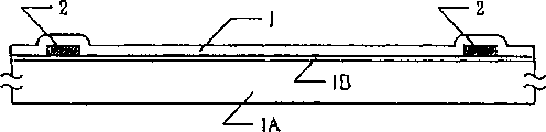
图2(A-1)、2(A-2)及2(B)~2(D)是表示实施例工艺(选择结晶工艺)的剖面图;Fig. 2 (A-1), 2 (A-2) and 2 (B)~2 (D) are the sectional views that represent embodiment technology (selective crystallization process);
图3(A)~3(C)是表示该实施例(见第一实施例)工艺的剖面图;Fig. 3 (A)~3 (C) are the sectional views that represent this embodiment (seeing first embodiment) process;
图4(A)~4(C)是表示该实施例(见第一实施例)工艺的剖面图;Fig. 4 (A)~4 (C) are the sectional views that represent this embodiment (seeing first embodiment) process;
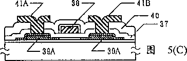
图5(A)~5(C)是表示该实施例(见第二实施例)工艺的剖面图;Fig. 5 (A)~5 (C) are the sectional views that represent this embodiment (see second embodiment) process;
图6(A)~6(C)是表示该实施例(见第三实施例)工艺的剖面图;Fig. 6 (A)~6 (C) are the cross-sectional views that represent this embodiment (seeing the 3rd embodiment) process;
图7(A)~7(E)是表示该实施例(见第四实施例)工艺的剖面图;Fig. 7 (A)~7 (E) are the sectional views that represent this embodiment (seeing the 4th embodiment) process;
图8(A)是当本发明被用于一有源矩阵装置之案例的方柜图:Fig. 8 (A) is when the present invention is used for the square cabinet diagram of the case of an active matrix device:
图8(B)是当本发明被用于一图象传感器的驱动电路的一个电路图;FIG. 8(B) is a circuit diagram of a driving circuit when the present invention is applied to an image sensor;
图9(A)~9(C)是表示该实施例工艺的剖面图;Fig. 9 (A)~9 (C) are the sectional views that represent this embodiment process;
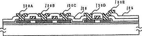
图10(A)~10(C)是表示该实施例工艺的剖面图;以及Fig. 10 (A)~10 (C) are the sectional views that represent this embodiment process; And
图11(A)~11(D)是表示该实施例工艺的剖面图。11(A) to 11(D) are sectional views showing the process of this embodiment.
实施例1Example 1
在本实施例中将介绍,用在Coning 7059玻璃衬底上形成的各个岛状镍膜作起始点,使非晶硅膜结晶化,用所得到的晶体硅膜制造TFT的方法。根据岛状镰膜是在非晶硅膜之上还是之下形成,则有两种形成岛状镍膜的方法。图2(A-1)表示在硅膜下形成镍膜的方法,而图2(A-2)表示在硅膜上形成镍膜的方法。对后一方法必须特别小心,因为在工艺中,有选择地腐蚀镍是在非晶硅膜的整个表面上形成镍之后,镍和非晶硅相互反应,尽管其量很少,将产生硅化镍。因为如果硅化镍照原样留下来,则不能得到好的结晶硅膜,本发明目的之在于,必须用氢氯酸或氢氟酸完全去掉硅化镍。因此,非晶硅从原始状态变薄些。In this embodiment, a method of crystallizing an amorphous silicon film using island-shaped nickel films formed on a Coning 7059 glass substrate as starting points, and manufacturing a TFT from the resulting crystalline silicon film will be described. There are two methods of forming the island-shaped nickel film depending on whether the island-shaped sickle film is formed on or under the amorphous silicon film. FIG. 2(A-1) shows a method of forming a nickel film under a silicon film, and FIG. 2(A-2) shows a method of forming a nickel film on a silicon film. Special care must be taken with the latter method, because in the process, nickel is selectively etched on the entire surface of the amorphous silicon film. After nickel is formed, nickel and amorphous silicon react with each other, although the amount is small, and nickel silicide will be produced. . Since a good crystalline silicon film cannot be obtained if nickel silicide is left as it is, it is an object of the present invention to completely remove nickel silicide with hydrochloric acid or hydrofluoric acid. Therefore, the amorphous silicon becomes thinner from the original state.
另一方面,对前一种情况,虽然没有引起这种问题,在此情况下,除岛状部分之外,也用腐蚀法完全去掉镍膜。用氧等离子或臭氧处理衬底,使岛区以外的镍氧化,可以排除残留镍的影响。On the other hand, in the former case, although no such problem is caused, in this case, the nickel film is also completely removed by etching except for the island-shaped portion. Treat the substrate with oxygen plasma or ozone to oxidize the nickel outside the island area, which can eliminate the influence of residual nickel.
不论哪一种情况,均用等离子CVD方法,在衬底1A(Coning7059)上形成厚度为2000Å的底层氧化硅膜1B。用等离子CVD方法或真空CVD法制备非晶硅膜1,厚200~3000Å,优选500~1500Å。基350~450℃退火0.1~2小时去氢,把膜内氢的浓度保持在5at%以下之后,容易使非晶硅膜结晶化。In either case, an underlying silicon oxide film 1B with a thickness of 2000Å was formed on a substrate 1A (Coning7059) by plasma CVD. The
就图2(A-1)而论,是在形成非晶硅膜1之前,用溅射法使镍膜堆积到50-1000Å,优选100-500Å,再刻图形成岛状镰区2。As far as Fig. 2 (A-1) is concerned, before forming the
就图2(A-2)而论,则相反,是在形成非晶硅膜1之后,用溅射法使镍膜堆积到50-1000Å,优选100-500Å,再刻图形成岛状镰区2。图1A表示上述的状态。As far as Fig. 2 (A-2) is concerned, on the contrary, after forming the
每个岛区镍是2×2μm的方形,间隔设定为5-50μm或例如20μm。用硅化镍代替镍,也取得了同样的效果。当要形成镍时,将衬底加热至100-500℃,优选180-250℃,能得到良好的结果。那是因为改进了底层硅化镍层与镍膜的粘附,还因为由氧化硅与镍反应产生硅化镍,用氮化硅、碳化硅或硅代替氧化硅也能得到相同的效果。Each nickel island is a 2×2 μm square, and the interval is set at 5-50 μm or, for example, 20 μm. Replacing nickel with nickel silicide also achieves the same effect. When nickel is to be formed, good results are obtained by heating the substrate to 100-500°C, preferably 180-250°C. That is because the adhesion of the underlying nickel silicide layer to the nickel film is improved, and because nickel silicide is produced by the reaction of silicon oxide with nickel, the same effect can be obtained by replacing silicon oxide with silicon nitride, silicon carbide or silicon.
然后在氮气气氛中在450-580℃或例如在550℃退火8小时。这退火也可以在氮和氢混合气氛中进行。或者,此退火可以在氢气气氛中进行X1小时,然后在氮气气氛中进行X2小时。图2(B)表示此工艺的中间状态,其中的镍从岛状镍区2推进到靠近中心的边缘,成为硅化镍3A,镍已通过的部位3已变成晶体硅。然后如图2(C)所示,从两个岛状镍膜起始的结晶化衔接,而硅化镍3A留在中间,从而结晶化结束。It is then annealed at 450-580°C or, for example, at 550°C for 8 hours in a nitrogen atmosphere. This annealing can also be performed in a nitrogen and hydrogen mixed atmosphere. Alternatively, this annealing may be performed in a hydrogen atmosphere for X1 hours, and then in a nitrogen atmosphere for X2 hours. Fig. 2(B) shows the intermediate state of this process, wherein the nickel advances from the island-shaped
图1(B)表示从上看此状态中的衬底,其中图2(C)中的硅化镍是晶间的边界4。当继续退火时,镍沿晶间边界4移动,聚集岛状镰区的中间区5(虽然在此状态下来保持它们原来的形状)。FIG. 1(B) shows the substrate in this state viewed from above, where nickel silicide in FIG. 2(C) is the
用上述工艺可以得到晶体硅,但不希望镍从在此时产生的硅化镰扩散到半导体涂覆膜中。最好用氢氯酸或氢氟酸腐蚀,消除镰高度集聚的区域。再有,因为镍和硅化镍的腐蚀速度十分大,在用氢氯酸或氢氟酸腐蚀时,硅膜不受影响。同时去掉原设置镍的生长点的区域。图2(D)表示腐蚀后的状态。原来是晶间边界的部位转变为一个槽4A。这对形成半导体TFT的区域(有源层或类似层)是不希望的,以致要收缩该槽。如图1(C)所示,不使半导体区6跨过晶间边界4来布局TFT。即,在平行衬底的水平方向,不在涂覆膜的厚度方向,在镍作用下的晶体生长区内形成TFT。应均匀安排晶体生长方向,还应尽量缩小残留的镍。另一方面,栅线7可以跨越晶间边界4。Crystalline silicon can be obtained by the above process, but diffusion of nickel into the semiconductor coating film from the silicide produced at this time is undesirable. It is best to etch with hydrochloric or hydrofluoric acid to remove areas of high sickle concentration. Furthermore, since the corrosion rate of nickel and nickel silicide is very high, the silicon film is not affected when it is etched with hydrochloric acid or hydrofluoric acid. At the same time, the area where the growth point of nickel was originally set is removed. Fig. 2(D) shows the state after corrosion. The portion which was originally an intergranular boundary is transformed into a
图3和图4表示用上述工艺得到的晶体硅制作TFT的方法实施例。在图3(A)中,中间的标号字符X指示图2中原来是槽4A的地方,如图所示,在布局半导体TFT区域时,不能跨过X部位。即,将图2所示工艺所得到晶体硅膜构图形成岛状半导体区11a和11b。然而,用诸如RF等离子CVD、ECR等离子CVD或溅射形成作为栅绝缘膜的氧化硅膜12。Fig. 3 and Fig. 4 show the embodiment of the method of making TFT by using the crystalline silicon obtained by the above process. In FIG. 3(A), the label character X in the middle indicates the
进一步,用真空CVD方法掺杂1×10²⁰~5×10²⁰/cm3的磷,形成厚3000~6000Å的多晶硅膜,然后将它构成图(图3(A)),形成栅电极13a和13b。Further, doping 1×10 20 to 5×10 20 /cm 3 of phosphorus by vacuum CVD method to form a polysilicon film with a thickness of 3000 to 6000 Å, and then forming it into a pattern (Fig. 3(A)), forming the gate electrode 13a and 13b.
然后,用等离子掺杂方法掺入杂质。至于掺杂气体,对N型TFT,使用磷化氢(PH3),对p型TFT.使用乙硼烷(B2H6)。对磷化氢加速电压是80KeV,对乙硼烷是65KeV。在550℃退火4小时,激活杂质,以形成杂质区14a到14b。用光能,如激光退火或闪光灯退火的方法,也可以用于激活(图3(B))。Then, impurities are doped by a plasma doping method. As for the doping gas, phosphine (PH 3 ) was used for the N-type TFT, and diborane (B 2 H 6 ) was used for the p-type TFT. The accelerating voltage for phosphine is 80KeV, and for diborane is 65KeV. Annealing at 550°C for 4 hours activates the impurities to form impurity regions 14a to 14b. The use of light energy, such as laser annealing or flash lamp annealing, can also be used for activation (Fig. 3(B)).
最后,淀积一层厚5000Å的氧化硅膜作为层间绝缘体15,与正常制作TFT的情况类似,通过该层形成接能孔,在源和漏区形成布线和电极16a~16d。Finally, deposit a layer of silicon oxide film with a thickness of 5000 Å as the
TFT(图中N沟型)就是按上述工艺制备的。所得到的TFT的场效应迁移率,在N沟型是40~60cm2/V.s,在P沟型是30~50cm2/V.s。TFT (N channel type in the figure) is prepared according to the above process. The field effect mobility of the obtained TFT was 40 to 60 cm 2 /Vs for the N channel type and 30 to 50 cm 2 /Vs for the P channel type.
图4表示如何制备铝栅TFT的工艺。在图4(A)中,中间的标号字符X指明原是图2中槽4A的地方。对半导体TFT区域的设置不应跨过X部位。即,将按图2所示工艺得到的晶体硅膜3构图形成岛状半导体区21a和21b。然后,用诸如RF等离子CVD、ECR等离子CVD或测射方法形成作为栅绝膜的氧化硅膜22。当用TEOS(四乙氧硅烷)和氧化原始气体掺杂等离子CVD方法时,能得到满意的效果。然后,溅射淀积含1%硅的铝膜(厚5000Å)再构图形成栅导线和电极23a和23b。FIG. 4 shows a process of how to fabricate an aluminum gate TFT. In FIG. 4(A), the reference character X in the middle indicates the place where the
接着,将衬底浸入3%酒石酸的乙烯乙二醇溶液中,设置镍作为阴极,铝线作阳极,再在二者间通以电流,实施阳极氧化。起初按2V/分增高其电压来施加电流,当达到220V时,将电压固定。当电流变成小于10μA/M2,停止通电,结果,如图4(A)所示形成厚2000Å的阳极氧化层24a和24b。Next, immerse the substrate in ethylene glycol solution of 3% tartaric acid, set nickel as the cathode, and aluminum wire as the anode, and then pass an electric current between the two to carry out anodic oxidation. Initially, the voltage was increased by 2V/min to apply the current, and when it reached 220V, the voltage was fixed. When the current became less than 10 µA/M 2 , the energization was stopped, and as a result, the
然后用等离子储杂方法掺入杂质。关于掺杂气体,对N型TFT用磷化氢(PH3),对P型TFT用乙硼烷(B2H6)。附图表示N型TFT。对磷化氢加速电压是80KeV,对乙硼烷是65KeV。用激光退火激活杂质,形成杂质区25a至25d。所用的激光是KrF激光(波长248nm),用能量密度为250~300mJ/cm2的激光脉冲辐照5次(图4(B))。Impurities are then doped by the plasma doping method. As for the doping gas, phosphine (PH 3 ) was used for N-type TFTs, and diborane (B 2 H 6 ) was used for P-type TFTs. The drawings show N-type TFTs. The accelerating voltage for phosphine is 80KeV, and for diborane is 65KeV. Impurities are activated by laser annealing to form impurity regions 25a to 25d. The laser used was a KrF laser (wavelength 248nm), which was irradiated 5 times with a laser pulse with an energy density of 250-300mJ/cm 2 (Fig. 4(B)).
最后,淀积厚5000Å的氧化硅膜,作为层间绝缘体26,类似于正常制备TFT的情况,通过该层形成接触孔,以便形成源和漏区的布线和电极27a~27d(图4(C))。Finally, a silicon oxide film with a thickness of 5000 Å is deposited as an interlayer insulator 26, similar to the case of normally preparing a TFT, and a contact hole is formed through this layer to form the wiring and electrodes 27a-27d of the source and drain regions (Fig. 4(C )).
所得到的TFT的场迁率是,在N沟型为60~120cm2/V.s,在P沟型TFT为50~90cm2/V.s。在用此种TFT制作的移位寄存器中,确认在17V的漏电压,工作在6MHz,在20V漏电压工作在11MHz。The field mobility of the obtained TFT was 60 to 120 cm 2 /Vs for an N-channel type TFT, and 50 to 90 cm 2 /Vs for a P-channel type TFT. In the shift register made with this kind of TFT, it is confirmed that the drain voltage of 17V works at 6MHz, and the drain voltage of 20V works at 11MHz.
实施例2Example 2
图5表示一种制作铝栅TFT的情况,与图4所示相似。然而,在此实施例中,非晶硅被用作有源层。如图5(A)所示,在衬底31上淀积一层厚2000~3000Å的非晶硅膜33。在非晶硅膜中可以混入适量的P型或N型杂质。按上所述形成岛状镰或硅化镍涂覆膜34A和34B,在此状态下,在550℃退火8小时,或在600℃退火4小时,使非晶硅膜横向生长而结晶化。FIG. 5 shows a case of fabricating an aluminum gate TFT, which is similar to that shown in FIG. 4 . However, in this embodiment, amorphous silicon is used as the active layer. As shown in FIG. 5(A), an
然后,将如此得到的晶体硅膜构成如图5(B)所示的图形,此时,因为在图中的中部(镍或硅化镍膜34A和34B之间的中间部位)的硅膜含有大量有镍,实施刻图时,要去掉此部位,以形成岛状硅区35A和35B。然后,在其上再淀积基本上本征的非晶硅膜36。Then, the thus obtained crystalline silicon film is formed into a pattern as shown in FIG. 5(B). Nickel is present, and when patterning is performed, this portion is removed to form island-
此后,如图5(C)所示,用诸如氮化硅或氧化硅之物质形成一层涂覆膜,作这栅绝缘膜37。用铝形成栅电极38,再用与图4情况相同的方法实施阳极氧化。然后用离子掺杂方法扩散杂质,以形成杂质区39A和39B。然后再淀积层间绝缘体40,形成接触孔以及在源的漏区形成金属电极41A和41B,完成TFT。该TFT的特征在于,在源和漏部位的半导体膜是厚的,其阻抗是小的。其结果,降低了源和漏区的阻抗,改进了TFT的特征。再有,接触可能容易形成接触孔。Thereafter, as shown in FIG. 5(C), a coating film is formed of a substance such as silicon nitride or silicon oxide as the
实施例3Example 3
图6表示制作CMOS型TFT的工艺过程。如图6(A)所示,在衬底51上淀积一底层氧化硅膜52,再在其上淀积一层厚1000~1500Å的非晶硅膜53。然后如上所述,形成岛状镍或硅化镍涂覆膜54,在此状态在550℃实施退火。硅化镍区55沿涂覆膜的平面方向,而不是厚度方向移位,以此工艺推进结晶化。退火4小时,使非晶硅膜变成如图6(B)所示晶体硅。硅化镍区59A和59B随着结晶化的推进被推向边缘。FIG. 6 shows a process for fabricating a CMOS type TFT. As shown in FIG. 6(A), an underlying silicon oxide film 52 is deposited on a substrate 51, and an amorphous silicon film 53 with a thickness of 1000˜1500Å is deposited thereon. Then, as described above, the island-shaped nickel or nickel silicide coating film 54 is formed, and annealing is performed at 550° C. in this state. The nickel silicide region 55 is shifted in the plane direction of the coating film, not in the thickness direction, and crystallization is promoted by this process. Annealing was performed for 4 hours to change the amorphous silicon film into crystalline silicon as shown in FIG. 6(B). The
将如此得到的晶体硅膜构图形成如图6(B)所示的岛状硅区56。这里应特别小心,镍被高度集聚在岛区的两端。在形成岛状硅区之后,形成栅绝缘膜57以及栅电极58A和58B。The crystalline silicon film thus obtained is patterned to form island-shaped silicon regions 56 as shown in FIG. 6(B). Special care should be taken here, nickel is highly concentrated at both ends of the island. After forming the island-shaped silicon regions, a
然后,用离子掺杂方法扩散杂质形成N型杂质区60A和P型杂质区60B,如图6(C)所示。此时,可以用磷作为N型杂质(掺杂气体是磷化氢PH3)进行掺杂,用60~110KeV的加速电压使掺杂遍布整个表面,然后用光刻胶覆盖N沟型TFT区,之后再。例如,用硼作为P型杂质(掺杂气体是乙硼烷B2H6),再用40~80KeV的加速电压进行掺杂。Then, impurities are diffused by ion doping to form N-type impurity regions 60A and P-type impurity regions 60B, as shown in FIG. 6(C). At this time, phosphorus can be used as N-type impurity (the doping gas is phosphine PH 3 ) for doping, and an accelerating voltage of 60-110KeV is used to spread the doping over the entire surface, and then cover the N-channel TFT region with photoresist , later. For example, boron is used as a P-type impurity (the doping gas is diborane B 2 H 6 ), and then doped with an accelerating voltage of 40-80 KeV.
掺杂后,用类似于图4情况的激光辐照,使源和漏区激活。然后,再淀积层间绝缘体61形成接触孔以及在源和漏区形成金属电极62A、62B和62C,制成TFT。After doping, the source and drain regions are activated by irradiating with laser light similar to the case in FIG. 4 . Then, an interlayer insulator 61 is deposited to form a contact hole and metal electrodes 62A, 62B and 62C are formed in the source and drain regions to form a TFT.
实施例4Example 4
图7表示第四个实施例。本实施例涉及一种方法,其中,用第一次热处理(预退火)使镍膜与非晶硅膜的一部分反应,在去掉来反应的镍膜后,再退火使非晶硅膜化,产生硅化物。Fig. 7 shows a fourth embodiment. This embodiment relates to a method in which the first heat treatment (pre-annealing) is used to make the nickel film react with a part of the amorphous silicon film, and after removing the reacted nickel film, annealing is performed to form the amorphous silicon film, resulting in silicide.
用溅射法在衬底(Coning No7059)701上形成一底层氧化硅膜702(厚2000Å)。然后,形成一层厚300~800Å,例如厚500Å的硅膜703。再用等离子CVD法形成一层氧化硅膜704。该氧化硅膜704用作掩膜材料,其厚度优选在500~2000Å。若太薄,因针孔使结晶化从意外的地方展开,若太厚,为形成厚膜要花更多时间,这不适于批量生产。因而这里设在1000Å。An underlying silicon oxide film 702 (thickness 2000 Å) was formed on a substrate (Coning No. 7059) 701 by sputtering. Then, a silicon film 703 with a thickness of 300˜800 Å, for example, a thickness of 500 Å is formed. A silicon oxide film 704 is then formed by plasma CVD. The silicon oxide film 704 is used as a mask material, and its thickness is preferably 500˜2000 Å. If it is too thin, crystallization will spread from unexpected places due to pinholes, and if it is too thick, it will take more time to form a thick film, which is not suitable for mass production. Therefore it is set at 1000Å here.
之后,用公知的光刻工艺,将氧化硅膜704构图。然后用溅射法形成一层镍膜705(厚500Å)。镍膜705的厚度最好比100Å厚[图7(A)]。Thereafter, the silicon oxide film 704 is patterned by a known photolithography process. Then a nickel film 705 (thickness 500 Å) was formed by sputtering. The thickness of the nickel film 705 is preferably thicker than 100 Å [FIG. 7(A)].
然后,使它在氮气气氛内,在250~450℃(一种预退火工艺)退火10~60分钟。例如,在450℃退火20分钟。结果,在非晶硅内形成一层硅化镍706。该层的厚度由预退火的温度和时间决定,而几乎与镍膜的厚度无关(图7(B))。Then, it is annealed at 250-450° C. (a pre-annealing process) for 10-60 minutes in a nitrogen atmosphere. For example, anneal at 450°C for 20 minutes. As a result, a layer of
之后,腐蚀该镰膜。硝酸或氢氯酸溶液适用于此腐蚀。在用这些腐蚀剂腐蚀镰膜过程中,硅化镍层几乎不被腐蚀。在本实施例中,使用一种在硝酸中加入作为缓冲剂的乙酸的腐蚀剂。其配比是:硝酸∶乙酸∶水=1∶10∶10。在去掉镍膜之后,在550℃退火4~8小时(一种结晶化退火工艺)。Thereafter, the sickle is etched. Nitric or hydrochloric acid solutions are suitable for this corrosion. During etching of the sickle film with these etchant, the nickel silicide layer is hardly etched. In this embodiment, an etchant in which acetic acid was added as a buffer to nitric acid was used. Its proportioning ratio is: nitric acid: acetic acid: water=1: 10: 10. After removing the nickel film, it is annealed at 550° C. for 4 to 8 hours (a crystallization annealing process).
在结晶化退火工艺中,试过数种方法。第一种方法,如图7(C)所示,在实施此工艺时,同时保留掩模材料704。结晶化按图7(C)箭头所指方向推进。第二种方法是在去掉所有的掩模露出硅膜之后进行退火。第三种方法是在去掉掩模材料之后,在硅膜上形成由氧化硅或氮化硅组成的作为保护膜的新的涂覆膜707之后,进行退火,如图7(D)所示。In the crystallization annealing process, several methods have been tried. In the first method, as shown in FIG. 7(C), the mask material 704 is retained while performing the process. Crystallization advances in the direction indicated by the arrow in Figure 7(C). The second method is to perform annealing after removing all the mask to expose the silicon film. The third method is to perform annealing after removing the mask material, after forming a
虽然第一种方法简单,但掩模材料704的表面在预退火步骤与镍的反应,并在更高温度的结晶化退火工艺中变成硅化物,几乎不能腐蚀。即,因为硅膜和掩模材料704的腐蚀速率几乎相等,为掩模材料去掉后,硅膜被露出的部位也大量被腐蚀,在衬底上产生台阶。Although the first method is simple, the surface of the mask material 704 reacts with nickel in the pre-annealing step, and becomes silicide in the crystallization annealing process at a higher temperature, which is hardly corroded. That is, since the etching rates of the silicon film and the mask material 704 are almost equal, after the mask material is removed, a large amount of exposed parts of the silicon film are also etched, and steps are generated on the substrate.
第二种方法很简单,很容易进行腐蚀,因为在结晶化退火工艺之前,掩模材料与镍的反应轻微。然而,当进行结晶化退火时,硅表面完全被暴露,后来制造的TFT或类似物的特性要变坏。The second method is simple and easy to etch because the mask material reacts slightly with nickel before the crystallization annealing process. However, when the crystallization annealing is performed, the silicon surface is completely exposed, and the characteristics of TFTs or the like manufactured later are deteriorated.
虽然第三种方法可以稳定地得到优质晶体硅膜,但很复杂,因为增加一些工艺过程。至于第四种方法,是第三种方法的一种改型,该方法包括;在硅表面被暴露的状态下,放入一个炉内,先通氧在500~550℃加热大约1小时,以便在表面形成厚20~60Å的薄氧化硅膜,作为对结晶化退火条件的探讨改为通氮。根据该方法,在结晶化起始阶段形成氧化膜。但在此氧化阶段只在硅化镍膜的附近被结晶化,后来将用作TFT的区(图中右侧部位),没有被结晶化。因此,在远离硅化镍层706的区域硅膜的表面是很平坦的。特性比第二种方法改进许多,与第三种方法几乎相等。Although the third method can stably obtain high-quality crystalline silicon film, it is very complicated because some processes are added. As for the fourth method, it is a modification of the third method, which includes: putting the silicon surface into a furnace in a state where the silicon surface is exposed, and heating at 500-550° C. for about 1 hour through oxygen, so that A thin silicon oxide film with a thickness of 20-60 Å is formed on the surface, and nitrogen is passed as a study on the annealing conditions for crystallization. According to this method, an oxide film is formed at the initial stage of crystallization. However, at this oxidation stage, only the vicinity of the nickel silicide film is crystallized, and the region to be used later as a TFT (right side in the figure) is not crystallized. Therefore, the surface of the silicon film is very flat in a region away from the
晶体硅膜是这样得到的。从此以后,将硅膜703构图,同时去掉镍浓度高的部位(设置生长起始区的区域)和生产点(在图中箭头末端的斜线部位),同时只保留镍浓度低的区域。按上所述,形成将用于TFT有源层的岛状硅区708。然后用等离子CVD形成厚1200Å由氧化硅构成的栅绝缘膜709,覆盖住区域708。再用厚6000Å的掺磷硅膜形成栅电极710和第一层的布线711,用栅电极710作掩模,以自对准方式,将杂质注入有源层708,形成源/漏区712。然后用可见或近红外强光辐照,对改进结晶化是有效的。再用等离子CVD法形成厚6000Å的氧化硅膜做层间绝缘体713。最后,在层间绝缘体中制出接触孔,再用厚6000Å的铝膜形成第二布线714、源/漏电极兼布线715。以上述的工艺完成TFT(图7(E))。The crystalline silicon film is thus obtained. Thereafter, the silicon film 703 is patterned while removing the high nickel concentration area (area where the growth initiation region is provided) and the production point (the oblique line at the end of the arrow in the figure), while leaving only the low nickel concentration area. As described above, the island-shaped silicon region 708 to be used for the TFT active layer is formed. Then, a gate insulating film 709 made of silicon oxide is formed to cover the region 708 to a thickness of 1200 Å by plasma CVD. Then use a phosphorus-doped silicon film with a thickness of 6000 Å to form the gate electrode 710 and the wiring 711 of the first layer, use the gate electrode 710 as a mask, and inject impurities into the active layer 708 in a self-aligned manner to form source/drain regions 712 . Then irradiating with strong visible or near-infrared light is effective for improving crystallization. Then, a silicon oxide film with a thickness of 6000 Å was formed as an interlayer insulator 713 by plasma CVD. Finally, a contact hole is made in the interlayer insulator, and then the second wiring 714 and the source/drain electrode and wiring 715 are formed with an aluminum film with a thickness of 6000 Å. The TFT is completed in the above-mentioned process (FIG. 7(E)).
实施例5Example 5
图9表示本实施例。在本实施例中,在TFT型液晶显示装置的有源矩阵区和外围电路中,形成多晶硅TFT。Fig. 9 shows this embodiment. In this embodiment, polysilicon TFTs are formed in the active matrix region and peripheral circuits of the TFT type liquid crystal display device.
首先,在有耐热性质的玻璃衬底如石英玻璃120上,用溅射法,淀积厚20~200nm的一底层氧化膜121。再用甲硅烷或乙硅烷作原材料,用等离子VCD法或真空CVD法,在其上淀积30~50nm的非晶硅膜。这里,氧或氮在非晶硅膜中的浓度低于1018/cm3。最好低于1017/cm3。本实施例中,将氧的浓度设置在低于1017/cm3。用溅射法在非晶硅膜上形成厚100-150nm的氧化硅膜或厚30-100nm的氮化硅膜作为覆盖膜。然后构图,仅留下外围电路区域的覆盖膜122。然后,在含20-100vol%的氧或氢的氩或氮的气氛中(600℃)保存4-100小时,使它结晶。结果,外围电路区的硅膜123A的结晶性是好的,而象素区的硅膜123B的结晶性不好。图9(A)示出此状态。First, on a heat-resistant glass substrate such as
接下来,将硅膜构成如图9(B)所示的用于形成外围电路TFT区124A和用于形成象素TFT区124B的岛状。然后用溅射法或类似方法形成栅氧化膜125。这可用TEOS(四乙氧硅烷)的等离子CVD法代替溅射法形成。当用TEOS形成该膜时,最好在形成当中或之后,在高于650℃的温度退火0.5-3小时。Next, the silicon film is formed into island shapes for forming the peripheral
在此之后,用LPCVD法形成厚0.2-2μm的N-型硅膜,并将它构成图形,在每个岛区形成栅电极126A-126C。具有较好耐热性能的金属材料,诸如钽、铬、钛、钨和钼可用来代替。After that, an N-type silicon film with a thickness of 0.2-2 µm is formed by LPCVD and patterned to form gate electrodes 126A-126C in each island region. Metallic materials with better heat resistance, such as tantalum, chromium, titanium, tungsten and molybdenum can be used instead.
然后,用栅电极部分作掩模,以自对准方式,用离子掺杂法,把杂质注入每个TFT的岛状硅膜。此时,首先采用磷化氢(PH3)作掺杂气体,把磷注入整个表面,然后用光刻胶覆盖图中右侧的岛区124A和矩阵区,之后采用乙硼烷(B2H4)作掺杂气体,把硼注入到左侧的岛区124A。磷的剂量设置为2-8×10¹⁵/cm2,而硼的剂量是4-10×1015/cm3,因此硼的剂量应超过磷的剂量。这样就产生一个P型区127A和N-型区127B及127C。Then, using the gate electrode portion as a mask, impurities are implanted into the island-shaped silicon film of each TFT by ion doping in a self-alignment manner. At this time, first use phosphine (PH 3 ) as the doping gas to inject phosphorus into the entire surface, then cover the
在550和750℃间的温度退火2-4小时进行激活它。本实施例中,在600℃进行热退火24小时。该退火工艺激活了离子注入区。It is activated by annealing at a temperature between 550 and 750°C for 2-4 hours. In this example, thermal annealing was performed at 600° C. for 24 hours. The annealing process activates the ion implantation region.
用激光退火可以完成此工艺。因为用激光退火时,对衬底的热损伤小,所以可以用普通无碱玻璃,例如,Conign7059。另外,可用耐热性差的材料如铝作栅电极材料。按上述的工艺产生了P型区127A及N-型区127B和127C。这些区的薄层电阻是200-800Ω/□。This process can be accomplished with laser annealing. Because the thermal damage to the substrate is small when laser annealing is used, common alkali-free glass, such as Conign7059, can be used. In addition, a material poor in heat resistance such as aluminum can be used as the gate electrode material. The P-type region 127A and N-type regions 127B and 127C are produced by the above-described process. The sheet resistance of these regions is 200-800Ω/□.
此后,用溅射法在整个表面形成厚300-1000nm的氧化硅膜,作为层间绝缘体128。这可以是用等离子CVD法形成的氧化硅膜。用等离子CVD法,特别是用TEOS作原材料,可以得到阶梯覆盖良好的氧化硅膜。Thereafter, a silicon oxide film is formed as an interlayer insulator 128 to a thickness of 300-1000 nm on the entire surface by sputtering. This may be a silicon oxide film formed by plasma CVD. A silicon oxide film with good step coverage can be obtained by plasma CVD, especially using TEOS as a raw material.
然后用溅射法产生一层ITO膜,再构图形成象素电极129。在TFT源/漏(杂质区)产生接触孔,以形成氮化钛或铬制成的布线130A-130E。图9(C)表示用左侧的NTFT和PTFT产生反向器电路。布线130A-130E可以是氮化钛或铬为底层的铝多层布线,以便降低薄层电阻。最后,在氢气中,在200-350℃退火0.5-2小时,以减少硅有源层的悬空键。外围电路和有源矩阵电路可一起集成。在本实施例中,在外围电路部,典型的迁移率对NMOS为80cm2/V·s,对PMOS为50cm2/v·s,而在象素TFT(NMOS)中,迁移率是5-30cm2/v·s。Then, a layer of ITO film is produced by sputtering, and then patterned to form the pixel electrode 129 . Contact holes are created in TFT source/drain (impurity regions) to form wirings 130A-130E made of titanium nitride or chrome. Fig. 9(C) shows that the NTFT and PTFT on the left are used to generate an inverter circuit. The
实施例6Example 6
图10表示本实施侧。在本实施例中,采用本发明减少CMOS电路中的NMOS和PMOS的迁移率之差。Fig. 10 shows the embodiment side. In this embodiment, the present invention is used to reduce the difference in mobility between NMOS and PMOS in a CMOS circuit.
首先,用溅射法在Coning7059衬底131上淀积厚20-200nm的底层氧化膜132。用甲硅烷或Z硅烷作原材料,用等离子CVD法或真空CVD法,再在其上淀积厚50-250nm的非晶硅膜。在非晶硅膜中氧或氮的浓度底低于1018/cm2或最好低于1017/cm3。为此目的,真空CVD法是适宜的。本发明中,氧浓度被设置为低于1017/cm3。First, an underlying oxide film 132 with a thickness of 20-200 nm is deposited on a Coning7059 substrate 131 by sputtering. Use monosilane or Z silane as a raw material, and deposit an amorphous silicon film with a thickness of 50-250 nm on it by plasma CVD or vacuum CVD. The concentration of oxygen or nitrogen in the amorphous silicon film is at least lower than 10 18 /cm 2 or preferably lower than 10 17 /cm 3 . For this purpose, a vacuum CVD method is suitable. In the present invention, the oxygen concentration is set to be lower than 10 17 /cm 3 .
在PMOS区上设置覆盖膜133(厚50-150nm的氧化硅膜)。然后在氩气或在含50%以上的氧或氢的氮的气氛中,在600℃退火4-100小时使之结晶化。其结果,在覆盏膜之下的区域134A的结晶性虽好,但无覆盖膜的区域134B结晶性却不好。图10(A)表示出此种状态。A cover film 133 (silicon oxide film with a thickness of 50-150 nm) is provided on the PMOS region. Then, it is annealed at 600°C for 4-100 hours in argon or in an atmosphere of nitrogen containing more than 50% oxygen or hydrogen to crystallize it. As a result, although the crystallinity of the
接着,将硅膜构成岛状,以便形成PMOS区135A和NMOS区135B,构图10(B)所示。Next, the silicon film is formed into an island shape to form a PMOS region 135A and an NMOS region 135B, as shown in Figure 10(B).
然后用溅射法形成厚50-150nm的氧化硅膜125,覆盖这些岛区作为栅绝缘膜136。然后用溅射法形成厚0.2-2um的铝膜,并构图形成栅电极。在电解液中给它输送电能,在栅电极之上和侧面形成阳极氧化膜。用上述的工艺在每个岛状区形成栅电极部分137A和137B。Then, a
然后,用离子掺杂法,用栅电极部分作掩膜以自对准方式,将杂质注入每个TFT的岛状硅膜。此时,首先用磷化氢(PH3)作掺杂气体,把磷注入整个表面,用光刻胶仅覆盖图中的岛区135B,用乙硼烷(B2H6)作掺杂气体,将硼注入岛区135A。磷的剂量设置为2-8×10¹⁵/cm3,硼的剂量设置为4-10×1015/cm2,以使硼的剂量超过磷的剂量。Then, by ion doping, impurities are implanted into the island-shaped silicon film of each TFT in a self-aligned manner using the gate electrode portion as a mask. At this time, first use phosphine (PH 3 ) as the doping gas, implant phosphorus into the entire surface, cover only the island region 135B in the figure with photoresist, and use diborane (B 2 H 6 ) as the doping gas , injecting boron into the island region 135A. The dose of phosphorus is set at 2-8×10 15 /cm 3 , and the dose of boron is set at 4-10×10 15 /cm 2 so that the dose of boron exceeds the dose of phosphorus.
虽然掺杂过程破坏了硅膜的结晶性,但它的薄层电阻仍可保持在1KΩ/□左右。然而,若此种程度的薄层电阻还高,再在600℃退火2-4小时,可降下薄层电阻。用强光或激光辐照可得到相同效果。Although the doping process destroys the crystallinity of the silicon film, its sheet resistance can still be maintained at around 1KΩ/□. However, if the sheet resistance is still high at this level, annealing at 600°C for 2-4 hours can reduce the sheet resistance. The same effect can be obtained with strong light or laser irradiation.
这样就形成了P型区138A和N-型区138B。这些区的薄层电阻为200-800Ω/□。然后用溅射法在整个表面上形成厚300-1000nm的氧化硅膜作层间绝缘体139。这可以是用等离子CVD法形成的氧化硅膜。用等离子CVD方法特别是用TEOS作原材料,可得到阶梯覆盖良好的氧化硅膜。This forms the P-
然后在TFT的源/漏(杂质区)形成接触孔,以形成铝布线140A-14OD。最后,在氢气中在250-350℃的温度退火2小时,以减少硅膜的悬空键。用上述工艺得到的TFT的典型迁移率,对PMOS和NMOS均为60cm2/v·s。当用本发明的工艺制作移位寄存器时,证实在20V的漏电压下,工作在10MHz以上。Contact holes are then formed in source/drain (impurity regions) of the TFTs to form aluminum wirings 140A-14OD. Finally, anneal at 250-350° C. for 2 hours in hydrogen to reduce dangling bonds of the silicon film. The typical mobility of TFT obtained by the above process is 60 cm 2 /v·s for both PMOS and NMOS. When the shift register is fabricated by the process of the present invention, it is confirmed that the shift register works above 10MHz under the leakage voltage of 20V.
实施例7Example 7
图11表示本实施例。本实施例涉及晶体管和硅电阻相结合的电路。用杂质掺杂的硅可用作晶体管的保护电路。首先,用溅射法在Coning 7059衬底140上淀积厚20-200nm的底氧化膜。在其上,再用等离子CVD法或真空CVD法,以甲硅烷或乙硅烷作原材料,淀积厚100-250nm的非晶硅膜。这里,在非晶硅膜中,氧或氯的浓度层低于1018/cm3,或最好低于1017/cm3。Fig. 11 shows this embodiment. This embodiment relates to a circuit in which transistors and silicon resistors are combined. Silicon doped with impurities can be used as a protective circuit for transistors. First, a bottom oxide film with a thickness of 20-200 nm is deposited on a Coning 7059
淀积厚20-200nm的氧化硅覆盏143,并在氩或氮的气氛中,在600℃退火4-100小时,使其结晶化。图11(A)表示出此状态。Deposit a silicon oxide cap 143 with a thickness of 20-200 nm, and anneal at 600° C. for 4-100 hours in an atmosphere of argon or nitrogen to crystallize it. Fig. 11(A) shows this state.
下面,将硅膜构成岛状,以形成晶体管区144A和电阻区144B,如图11(B)所示。然后用溅射法形成厚50-150nm的氧化硅膜覆盖那些岛区作栅绝缘膜145。然后,用溅射法形成厚0.2-2um的铝膜,再构图形成栅电极。给在电解液内的铝膜输送电能,在栅电极的上部和侧面形成阴极氧化膜。用上述的工艺,在每个岛区上,形成栅电极部分146。Next, the silicon film is formed into an island shape to form a transistor region 144A and a resistor region 144B, as shown in FIG. 11(B). A silicon oxide film is then formed to cover those island regions as a gate insulating film 145 to a thickness of 50 to 150 nm by sputtering. Then, an aluminum film with a thickness of 0.2-2um is formed by sputtering, and then patterned to form a gate electrode. Electric energy is sent to the aluminum film in the electrolyte, and a cathode oxide film is formed on the upper part and the side of the gate electrode. Using the above-mentioned process, on each island region, a gate electrode portion 146 is formed.
然后,用栅电极部分作掩膜,以自对准方式,用离子掺杂法,把杂质,如磷注入到每个TFT的岛状硅膜。磷的剂量为2-8×10¹⁵/cm2。Then, using the gate electrode portion as a mask, impurities such as phosphorus are implanted into the island-shaped silicon film of each TFT by ion doping in a self-alignment manner. The dosage of phosphorus is 2-8×10 15 /cm 2 .
用上述的掺杂工艺形成杂质区147A和147B。因为相同的杂质量被注入到两个掺杂区,当按照实际的要求热退火时,它们表示出相同的电阻率。然而,情况却是,例如当对后者要求较高的电阻时,而前者反倒要求较低的电阻。然后,仅在晶体管区,如图11(C)所示,形成厚50-150nm的氧化硅覆盖膜148。然后在含大于50vol%的氩或氢的氮或氩的气氛中,在550-650℃的温度,退火4-20小时。可用磷化氢代替氧或氢。然而,退火温度最好低于800℃,因为倘若退火温度太高,磷化氢将被热分解,并扩散到半导体中,反而降低了电阻率。当杂质的电阻区是P-型时,可以用乙硼烷(B2H6)。The impurity regions 147A and 147B are formed by the doping process described above. Since the same amount of impurity is implanted into the two doped regions, they exhibit the same resistivity when thermally annealed as desired. However, it is the case, for example, when a higher resistance is required for the latter, whereas a lower resistance is required for the former instead. Then, only in the transistor region, as shown in FIG. 11(C), a silicon oxide capping film 148 is formed to a thickness of 50 to 150 nm. Then annealing is carried out at a temperature of 550-650° C. for 4-20 hours in an atmosphere of nitrogen or argon containing more than 50 vol % of argon or hydrogen. Phosphine can be used instead of oxygen or hydrogen. However, the annealing temperature is preferably lower than 800°C, because if the annealing temperature is too high, phosphine will be thermally decomposed and diffused into the semiconductor, reducing the resistivity instead. When the resistance region of the impurity is P-type, diborane (B 2 H 6 ) can be used.
用上面的工艺,当晶体管的杂质区的薄层电阻是20-800Ω/□时,电阻的杂质区的薄层电阻是2K-100KΩ/□。用溅射法在整个表面上形成厚300-1000nm的氧化硅膜,作为层间绝缘体149。这可以是用等离子CVD法形成的氧化硅膜。用等离子CVD法,特别是用TEOS作原材料,可以得到覆盖阶梯良好的氧化硅膜。With the above process, when the sheet resistance of the impurity region of the transistor is 20-800Ω/□, the sheet resistance of the impurity region of the resistor is 2K-100KΩ/□. A silicon oxide film is formed as an interlayer insulator 149 to a thickness of 300-1000 nm on the entire surface by sputtering. This may be a silicon oxide film formed by plasma CVD. A silicon oxide film with good step coverage can be obtained by plasma CVD, especially using TEOS as a raw material.
在TFT的源/漏(杂质区)形成接触孔,以形成铝布线150A-150C。最后,在氢气中在250-350℃温度退火0.5-2小时,以便减少硅膜悬空键。经上述工艺可区分其厚度相同,杂质注入量相同的区域的薄层电阻。Contact holes are formed in source/drain (impurity regions) of TFTs to form aluminum wirings 150A-150C. Finally, anneal at 250-350° C. for 0.5-2 hours in hydrogen to reduce dangling bonds in the silicon film. Through the above process, the sheet resistance of regions with the same thickness and the same amount of impurity implantation can be distinguished.
如上所述,在某种意义上说,本发明是个划时代的发明,这促进了非晶硅在较低温度和较短时间实现结晶化,并为工业提供不可估量的效益,因为所用的设施、仪器和技术很普通的,而对批量生产则是极为优良的。虽然在前述的实施例中,着重对镍进行了解释,而同样的工艺可适用于另一些加速结晶化的金属元素,例如Fe、Co、Ru、Rh、Pd、Os、Ir、Pt、Sc、Ti、V、Cr、Mn、Cu、Zn、Au和Ag中的任一元素。As mentioned above, in a sense, the present invention is an epoch-making invention, which promotes the crystallization of amorphous silicon at a lower temperature and in a shorter time, and provides inestimable benefits for the industry, because the facilities used, The instruments and techniques are ordinary, yet excellent for mass production. Although in the foregoing embodiments, nickel has been emphatically explained, the same process can be applied to other metal elements that accelerate crystallization, such as Fe, Co, Ru, Rh, Pd, Os, Ir, Pt, Sc, Any element among Ti, V, Cr, Mn, Cu, Zn, Au and Ag.
例如,假定处理一片衬底须花两分钟,而在常规固相生长方法中需要15个退火炉,因为至少需要24小时的退火。本发明可使退火炉的数减到小于1/6,因为退火时间可缩短到4小时或更短的时间。由于衬底加工成本的下降,以及TFT成本的下降,以此生产率的提高、设备投资的降低以及因此而来的新需求的上升。所以,本发明对工业是很有利的,理所当然地应获得专利。For example, assuming that it takes two minutes to process one substrate, 15 annealing furnaces are required in the conventional solid phase growth method because at least 24 hours of annealing are required. The present invention can reduce the number of annealing furnaces to less than 1/6 because the annealing time can be shortened to 4 hours or less. Due to the decrease of substrate processing cost and the decrease of TFT cost, the increase of productivity, the decrease of equipment investment and the increase of new demand come from it. Therefore, the present invention is very beneficial to the industry and should be granted a patent as a matter of course.
另外,本发明以TFT有源层结晶条件的最小改动一有或者无覆盖膜,解决了常规的结晶硅TFT生产工艺中的难题。In addition, the present invention solves the difficult problems in the conventional crystalline silicon TFT production process with the minimum change of the crystallization conditions of the TFT active layer—with or without a covering film.
本发明尤其可改进动态电路和具有该电路的装置的可靠性和性能。一般,虽然对液晶显示的有源矩阵来说,结晶硅TFT的ON/OFF比是低的,并无论如何均难以投入实用,本发明认为这类问题已被解决。虽然未以实施例表明,很清楚,当实施本发明时,将TFT用作实施立体单晶半导体集成电器的装置会是有效的。In particular, the invention may improve the reliability and performance of dynamic circuits and devices incorporating such circuits. In general, although the ON/OFF ratio of crystalline silicon TFTs is low for active matrices of liquid crystal displays and is difficult to put into practical use anyway, the present invention considers that such problems have been solved. Although not shown in the examples, it is clear that when implementing the present invention, it is effective to use a TFT as a means for implementing a three-dimensional single crystal semiconductor integrated circuit.
例如,可用半导体电路知单晶半导体上做成外围逻辑电路,并通过层间绝缘体中介物,在其上设置TFT,来构成存储元件部分。在此情况下,存储元件部分可以是利用本发明的TFT的DRAM电路,而它们驱动电路是由被做成单晶半导体电路的CMOS构成。再有,当此种电路被用于微处理机时,可节省其面积,因为可把存储器部分在上层制造,认为本发明对工业是很有用的发明。For example, a peripheral logic circuit can be formed on a semiconductor circuit known as a single crystal semiconductor, and a TFT can be provided thereon via an interlayer insulator interposer to form a memory element portion. In this case, the memory element portion may be a DRAM circuit using the TFT of the present invention, and their driving circuit may be formed of a CMOS formed as a single crystal semiconductor circuit. Also, when this circuit is used in a microprocessor, its area can be saved because the memory part can be fabricated on the upper layer, and the present invention is considered to be a very useful invention for industry.
虽然参照其优选实施例已特别表示和介绍了本发明,但本领域的技术人员应了解到,在形式和细节上可以进行上述的和其它的改变,仍不应脱离本发明的精神和范畴。While the present invention has been particularly shown and described with reference to preferred embodiments thereof, those skilled in the art will recognize that the above and other changes may be made in form and detail without departing from the spirit and scope of the invention.
Claims (1)
Applications Claiming Priority (6)
| Application Number | Priority Date | Filing Date | Title |
|---|---|---|---|
| JP35054592 | 1992-12-04 | ||
| JP350545/92 | 1992-12-04 | ||
| JP5204775A JP2852853B2 (en) | 1993-07-27 | 1993-07-27 | Method for manufacturing semiconductor device |
| JP204775/93 | 1993-07-27 | ||
| JP298944/93 | 1993-11-04 | ||
| JP29894493 | 1993-11-04 |
Related Parent Applications (1)
| Application Number | Title | Priority Date | Filing Date |
|---|---|---|---|
| CN96114412A Division CN1091943C (en) | 1992-12-04 | 1996-11-01 | Method for manufacturing semiconductor device |
Related Child Applications (2)
| Application Number | Title | Priority Date | Filing Date |
|---|---|---|---|
| CNB2004100696546A Division CN100437907C (en) | 1992-12-04 | 1993-12-04 | Semiconductor device and manufacturing method thereof |
| CN2005100094014A Division CN1658389B (en) | 1992-12-04 | 1993-12-04 | Semiconductor device and manufacturing method thereof |
Publications (2)
| Publication Number | Publication Date |
|---|---|
| CN1348199A CN1348199A (en) | 2002-05-08 |
| CN1299331C true CN1299331C (en) | 2007-02-07 |
Family
ID=27328405
Family Applications (6)
| Application Number | Title | Priority Date | Filing Date |
|---|---|---|---|
| CN2005100094014A Expired - Lifetime CN1658389B (en) | 1992-12-04 | 1993-12-04 | Semiconductor device and manufacturing method thereof |
| CN93121667A Expired - Lifetime CN1052570C (en) | 1992-12-04 | 1993-12-04 | Semiconductor device and method for manufacturing the same |
| CNB2004100696546A Expired - Lifetime CN100437907C (en) | 1992-12-04 | 1993-12-04 | Semiconductor device and manufacturing method thereof |
| CN96114412A Expired - Lifetime CN1091943C (en) | 1992-12-04 | 1996-11-01 | Method for manufacturing semiconductor device |
| CNB001038338A Expired - Lifetime CN1149634C (en) | 1992-12-04 | 2000-02-28 | Manufacturing method of semiconductor device |
| CNB011330945A Expired - Lifetime CN1299331C (en) | 1992-12-04 | 2001-09-13 | Semiconductor device and manufacturing method thereof |
Family Applications Before (5)
| Application Number | Title | Priority Date | Filing Date |
|---|---|---|---|
| CN2005100094014A Expired - Lifetime CN1658389B (en) | 1992-12-04 | 1993-12-04 | Semiconductor device and manufacturing method thereof |
| CN93121667A Expired - Lifetime CN1052570C (en) | 1992-12-04 | 1993-12-04 | Semiconductor device and method for manufacturing the same |
| CNB2004100696546A Expired - Lifetime CN100437907C (en) | 1992-12-04 | 1993-12-04 | Semiconductor device and manufacturing method thereof |
| CN96114412A Expired - Lifetime CN1091943C (en) | 1992-12-04 | 1996-11-01 | Method for manufacturing semiconductor device |
| CNB001038338A Expired - Lifetime CN1149634C (en) | 1992-12-04 | 2000-02-28 | Manufacturing method of semiconductor device |
Country Status (4)
| Country | Link |
|---|---|
| US (3) | US5403772A (en) |
| KR (1) | KR970004450B1 (en) |
| CN (6) | CN1658389B (en) |
| TW (1) | TW226478B (en) |
Families Citing this family (303)
| Publication number | Priority date | Publication date | Assignee | Title |
|---|---|---|---|---|
| EP0445535B1 (en) | 1990-02-06 | 1995-02-01 | Sel Semiconductor Energy Laboratory Co., Ltd. | Method of forming an oxide film |
| US6008078A (en) | 1990-07-24 | 1999-12-28 | Semiconductor Energy Laboratory Co., Ltd. | Method for manufacturing a semiconductor device |
| US6975296B1 (en) * | 1991-06-14 | 2005-12-13 | Semiconductor Energy Laboratory Co., Ltd. | Electro-optical device and method of driving the same |
| JP3255942B2 (en) | 1991-06-19 | 2002-02-12 | 株式会社半導体エネルギー研究所 | Method for manufacturing inverted staggered thin film transistor |
| CN100465742C (en) | 1992-08-27 | 2009-03-04 | 株式会社半导体能源研究所 | Active matrix display |
| US5604360A (en) * | 1992-12-04 | 1997-02-18 | Semiconductor Energy Laboratory Co., Ltd. | Semiconductor device including a plurality of thin film transistors at least some of which have a crystalline silicon film crystal-grown substantially in parallel to the surface of a substrate for the transistor |
| US5403762A (en) * | 1993-06-30 | 1995-04-04 | Semiconductor Energy Laboratory Co., Ltd. | Method of fabricating a TFT |
| TW226478B (en) * | 1992-12-04 | 1994-07-11 | Semiconductor Energy Res Co Ltd | Semiconductor device and method for manufacturing the same |
| US6323071B1 (en) * | 1992-12-04 | 2001-11-27 | Semiconductor Energy Laboratory Co., Ltd. | Method for forming a semiconductor device |
| US5985741A (en) * | 1993-02-15 | 1999-11-16 | Semiconductor Energy Laboratory Co., Ltd. | Semiconductor device and method of fabricating the same |
| US6997985B1 (en) | 1993-02-15 | 2006-02-14 | Semiconductor Energy Laboratory Co., Ltd. | Semiconductor, semiconductor device, and method for fabricating the same |
| JP3562588B2 (en) * | 1993-02-15 | 2004-09-08 | 株式会社半導体エネルギー研究所 | Method for manufacturing semiconductor device |
| EP1119053B1 (en) * | 1993-02-15 | 2011-11-02 | Semiconductor Energy Laboratory Co., Ltd. | Method for fabricating TFT semiconductor device |
| KR0143873B1 (en) * | 1993-02-19 | 1998-08-17 | 순페이 야마자끼 | Insulating film and semiconductor device and method of manufacturing semiconductor device |
| US7465679B1 (en) | 1993-02-19 | 2008-12-16 | Semiconductor Energy Laboratory Co., Ltd. | Insulating film and method of producing semiconductor device |
| JP3107941B2 (en) * | 1993-03-05 | 2000-11-13 | 株式会社半導体エネルギー研究所 | Thin film transistor and manufacturing method thereof |
| JP3637069B2 (en) | 1993-03-12 | 2005-04-06 | 株式会社半導体エネルギー研究所 | Method for manufacturing semiconductor device |
| US6413805B1 (en) * | 1993-03-12 | 2002-07-02 | Semiconductor Energy Laboratory Co., Ltd. | Semiconductor device forming method |
| TW241377B (en) * | 1993-03-12 | 1995-02-21 | Semiconductor Energy Res Co Ltd | |
| US5569936A (en) * | 1993-03-12 | 1996-10-29 | Semiconductor Energy Laboratory Co., Ltd. | Semiconductor device employing crystallization catalyst |
| JP3193803B2 (en) * | 1993-03-12 | 2001-07-30 | 株式会社半導体エネルギー研究所 | Manufacturing method of semiconductor element |
| US5501989A (en) * | 1993-03-22 | 1996-03-26 | Semiconductor Energy Laboratory Co., Ltd. | Method of making semiconductor device/circuit having at least partially crystallized semiconductor layer |
| JP3535205B2 (en) * | 1993-03-22 | 2004-06-07 | 株式会社半導体エネルギー研究所 | Method for manufacturing thin film transistor |
| US5481121A (en) * | 1993-05-26 | 1996-01-02 | Semiconductor Energy Laboratory Co., Ltd. | Semiconductor device having improved crystal orientation |
| KR100355938B1 (en) * | 1993-05-26 | 2002-12-16 | 가부시키가이샤 한도오따이 에네루기 켄큐쇼 | Semiconductor device manufacturing method |
| US6090646A (en) * | 1993-05-26 | 2000-07-18 | Semiconductor Energy Laboratory Co., Ltd. | Method for producing semiconductor device |
| US5818076A (en) * | 1993-05-26 | 1998-10-06 | Semiconductor Energy Laboratory Co., Ltd. | Transistor and semiconductor device |
| US6875628B1 (en) * | 1993-05-26 | 2005-04-05 | Semiconductor Energy Laboratory Co., Ltd. | Semiconductor device and fabrication method of the same |
| KR100186886B1 (en) * | 1993-05-26 | 1999-04-15 | 야마자끼 승페이 | Semiconductor device manufacturing method |
| JP3157985B2 (en) | 1993-06-10 | 2001-04-23 | 三菱電機株式会社 | Thin film transistor and method of manufacturing the same |
| JPH06349735A (en) * | 1993-06-12 | 1994-12-22 | Semiconductor Energy Lab Co Ltd | Semiconductor device |
| JP3450376B2 (en) * | 1993-06-12 | 2003-09-22 | 株式会社半導体エネルギー研究所 | Method for manufacturing semiconductor device |
| US5488000A (en) * | 1993-06-22 | 1996-01-30 | Semiconductor Energy Laboratory Co., Ltd. | Method of fabricating a thin film transistor using a nickel silicide layer to promote crystallization of the amorphous silicon layer |
| US6713330B1 (en) | 1993-06-22 | 2004-03-30 | Semiconductor Energy Laboratory Co., Ltd. | Method of fabricating a thin film transistor |
| JP2677167B2 (en) * | 1993-07-08 | 1997-11-17 | 日本電気株式会社 | Method for manufacturing liquid crystal display device with built-in drive circuit |
| US5985704A (en) | 1993-07-27 | 1999-11-16 | Semiconductor Energy Laboratory Co., Ltd. | Method for manufacturing a semiconductor device |
| US5529937A (en) * | 1993-07-27 | 1996-06-25 | Semiconductor Energy Laboratory Co., Ltd. | Process for fabricating thin film transistor |
| US5663077A (en) | 1993-07-27 | 1997-09-02 | Semiconductor Energy Laboratory Co., Ltd. | Method of manufacturing a thin film transistor in which the gate insulator comprises two oxide films |
| US5589406A (en) * | 1993-07-30 | 1996-12-31 | Ag Technology Co., Ltd. | Method of making TFT display |
| US5492843A (en) * | 1993-07-31 | 1996-02-20 | Semiconductor Energy Laboratory Co., Ltd. | Method of fabricating semiconductor device and method of processing substrate |
| JP2975973B2 (en) * | 1993-08-10 | 1999-11-10 | 株式会社半導体エネルギー研究所 | Semiconductor device and manufacturing method thereof |
| JP2762215B2 (en) * | 1993-08-12 | 1998-06-04 | 株式会社半導体エネルギー研究所 | Method for manufacturing thin film transistor and semiconductor device |
| JPH0766424A (en) * | 1993-08-20 | 1995-03-10 | Semiconductor Energy Lab Co Ltd | Semiconductor device and manufacturing method thereof |
| JP2814049B2 (en) | 1993-08-27 | 1998-10-22 | 株式会社半導体エネルギー研究所 | Semiconductor device and manufacturing method thereof |
| KR100291971B1 (en) * | 1993-10-26 | 2001-10-24 | 야마자끼 순페이 | Substrate processing apparatus and method and thin film semiconductor device manufacturing method |
| TW264575B (en) * | 1993-10-29 | 1995-12-01 | Handotai Energy Kenkyusho Kk | |
| US5624873A (en) * | 1993-11-12 | 1997-04-29 | The Penn State Research Foundation | Enhanced crystallization of amorphous films |
| US5654203A (en) * | 1993-12-02 | 1997-08-05 | Semiconductor Energy Laboratory, Co., Ltd. | Method for manufacturing a thin film transistor using catalyst elements to promote crystallization |
| US5869362A (en) * | 1993-12-02 | 1999-02-09 | Semiconductor Energy Laboratory Co., Ltd. | Method of manufacturing semiconductor device |
| JP2860869B2 (en) * | 1993-12-02 | 1999-02-24 | 株式会社半導体エネルギー研究所 | Semiconductor device and manufacturing method thereof |
| US6798023B1 (en) * | 1993-12-02 | 2004-09-28 | Semiconductor Energy Laboratory Co., Ltd. | Semiconductor device comprising first insulating film, second insulating film comprising organic resin on the first insulating film, and pixel electrode over the second insulating film |
| CN100472752C (en) * | 1993-12-02 | 2009-03-25 | 株式会社半导体能源研究所 | Manufacturing method of semiconductor device |
| TW272319B (en) * | 1993-12-20 | 1996-03-11 | Sharp Kk | |
| KR100319332B1 (en) * | 1993-12-22 | 2002-04-22 | 야마자끼 순페이 | Semiconductor device and electro-optical device |
| TW279275B (en) * | 1993-12-27 | 1996-06-21 | Sharp Kk | |
| JP3221473B2 (en) * | 1994-02-03 | 2001-10-22 | 株式会社半導体エネルギー研究所 | Method for manufacturing semiconductor device |
| JP3378078B2 (en) * | 1994-02-23 | 2003-02-17 | 株式会社半導体エネルギー研究所 | Method for manufacturing semiconductor device |
| US6884698B1 (en) * | 1994-02-23 | 2005-04-26 | Semiconductor Energy Laboratory Co., Ltd. | Method for manufacturing semiconductor device with crystallization of amorphous silicon |
| KR100321541B1 (en) | 1994-03-09 | 2002-06-20 | 야마자끼 순페이 | How Active Matrix Display Devices Work |
| US6723590B1 (en) | 1994-03-09 | 2004-04-20 | Semiconductor Energy Laboratory Co., Ltd. | Method for laser-processing semiconductor device |
| US6700133B1 (en) | 1994-03-11 | 2004-03-02 | Semiconductor Energy Laboratory Co., Ltd. | Method for producing semiconductor device |
| JP3150840B2 (en) * | 1994-03-11 | 2001-03-26 | 株式会社半導体エネルギー研究所 | Method for manufacturing semiconductor device |
| US6974763B1 (en) | 1994-04-13 | 2005-12-13 | Semiconductor Energy Laboratory Co., Ltd. | Method of forming semiconductor device by crystallizing amorphous silicon and forming crystallization promoting material in the same chamber |
| KR100279217B1 (en) * | 1994-04-13 | 2001-02-01 | 야마자끼 순페이 | Semiconductor device formation method, crystalline semiconductor film formation method, thin film transistor formation method and semiconductor device manufacturing method |
| JP3192546B2 (en) * | 1994-04-15 | 2001-07-30 | シャープ株式会社 | Semiconductor device and method of manufacturing the same |
| US6433361B1 (en) * | 1994-04-29 | 2002-08-13 | Semiconductor Energy Laboratory Co., Ltd. | Semiconductor integrated circuit and method for forming the same |
| US6133620A (en) | 1995-05-26 | 2000-10-17 | Semiconductor Energy Laboratory Co., Ltd. | Semiconductor device and process for fabricating the same |
| JP3403812B2 (en) * | 1994-05-31 | 2003-05-06 | 株式会社半導体エネルギー研究所 | Method for manufacturing semiconductor device using thin film transistor |
| JP3540012B2 (en) * | 1994-06-07 | 2004-07-07 | 株式会社半導体エネルギー研究所 | Semiconductor device manufacturing method |
| US6867432B1 (en) * | 1994-06-09 | 2005-03-15 | Semiconductor Energy Lab | Semiconductor device having SiOxNy gate insulating film |
| JP3190520B2 (en) * | 1994-06-14 | 2001-07-23 | 株式会社半導体エネルギー研究所 | Semiconductor device and manufacturing method thereof |
| JP3067949B2 (en) * | 1994-06-15 | 2000-07-24 | シャープ株式会社 | Electronic device and liquid crystal display device |
| TW273639B (en) * | 1994-07-01 | 1996-04-01 | Handotai Energy Kenkyusho Kk | Method for producing semiconductor device |
| TW280943B (en) * | 1994-07-15 | 1996-07-11 | Sharp Kk | |
| JP3897826B2 (en) * | 1994-08-19 | 2007-03-28 | 株式会社半導体エネルギー研究所 | Active matrix display device |
| JP3464285B2 (en) * | 1994-08-26 | 2003-11-05 | 株式会社半導体エネルギー研究所 | Method for manufacturing semiconductor device |
| JPH0869967A (en) * | 1994-08-26 | 1996-03-12 | Semiconductor Energy Lab Co Ltd | Method for manufacturing semiconductor device |
| TW403993B (en) * | 1994-08-29 | 2000-09-01 | Semiconductor Energy Lab | Semiconductor circuit for electro-optical device and method of manufacturing the same |
| JP3442500B2 (en) | 1994-08-31 | 2003-09-02 | 株式会社半導体エネルギー研究所 | Method for manufacturing semiconductor circuit |
| TW374247B (en) * | 1994-09-15 | 1999-11-11 | Semiconductor Energy Lab Co Ltd | Method of fabricating semiconductor device |
| US6670640B1 (en) | 1994-09-15 | 2003-12-30 | Semiconductor Energy Laboratory Co., Ltd. | Method for producing semiconductor device |
| JP4083821B2 (en) * | 1994-09-15 | 2008-04-30 | 株式会社半導体エネルギー研究所 | Method for manufacturing semiconductor device |
| US6242289B1 (en) | 1995-09-08 | 2001-06-05 | Semiconductor Energy Laboratories Co., Ltd. | Method for producing semiconductor device |
| US5712191A (en) * | 1994-09-16 | 1998-01-27 | Semiconductor Energy Laboratory Co., Ltd. | Method for producing semiconductor device |
| US5915174A (en) * | 1994-09-30 | 1999-06-22 | Semiconductor Energy Laboratory Co., Ltd. | Semiconductor device and method for producing the same |
| US6300659B1 (en) | 1994-09-30 | 2001-10-09 | Semiconductor Energy Laboratory Co., Ltd. | Thin-film transistor and fabrication method for same |
| JPH08153879A (en) * | 1994-11-26 | 1996-06-11 | Semiconductor Energy Lab Co Ltd | Method for manufacturing semiconductor device |
| JP3418647B2 (en) * | 1994-12-09 | 2003-06-23 | 株式会社半導体エネルギー研究所 | Semiconductor device manufacturing method and crystal growth promoter |
| US6337229B1 (en) * | 1994-12-16 | 2002-01-08 | Semiconductor Energy Laboratory Co., Ltd. | Method of making crystal silicon semiconductor and thin film transistor |
| JP3469337B2 (en) * | 1994-12-16 | 2003-11-25 | 株式会社半導体エネルギー研究所 | Method for manufacturing semiconductor device |
| US5986311A (en) * | 1997-05-19 | 1999-11-16 | Citizen Watch Company, Ltd. | Semiconductor device having recrystallized source/drain regions |
| US6331475B1 (en) * | 1995-01-12 | 2001-12-18 | Semiconductor Energy Laboratory Co., Ltd. | Method and manufacturing semiconductor device |
| JP4130237B2 (en) * | 1995-01-28 | 2008-08-06 | 株式会社半導体エネルギー研究所 | Method for manufacturing crystalline silicon film and method for manufacturing semiconductor device |
| JP3138169B2 (en) * | 1995-03-13 | 2001-02-26 | シャープ株式会社 | Method for manufacturing semiconductor device |
| KR100265179B1 (en) * | 1995-03-27 | 2000-09-15 | 야마자끼 순페이 | Semiconductor device and manufacturing method |
| TW448584B (en) * | 1995-03-27 | 2001-08-01 | Semiconductor Energy Lab | Semiconductor device and a method of manufacturing the same |
| US7075002B1 (en) | 1995-03-27 | 2006-07-11 | Semiconductor Energy Laboratory Company, Ltd. | Thin-film photoelectric conversion device and a method of manufacturing the same |
| US5748268A (en) * | 1995-03-30 | 1998-05-05 | Kaiser Aerospace & Electronics Co. | Quasi-tiled active matrix display |
| US5536676A (en) * | 1995-04-03 | 1996-07-16 | National Science Council | Low temperature formation of silicided shallow junctions by ion implantation into thin silicon films |
| US6933182B1 (en) * | 1995-04-20 | 2005-08-23 | Semiconductor Energy Laboratory Co., Ltd. | Method of manufacturing a semiconductor device and manufacturing system thereof |
| TW463378B (en) | 1995-06-01 | 2001-11-11 | Semiconductor Energy Lab | Method of manufacturing semiconductor device |
| US5719033A (en) * | 1995-06-28 | 1998-02-17 | Motorola, Inc. | Thin film transistor bio/chemical sensor |
| US6120588A (en) * | 1996-07-19 | 2000-09-19 | E Ink Corporation | Electronically addressable microencapsulated ink and display thereof |
| JP3744980B2 (en) * | 1995-07-27 | 2006-02-15 | 株式会社半導体エネルギー研究所 | Semiconductor device |
| JP4056571B2 (en) | 1995-08-02 | 2008-03-05 | 株式会社半導体エネルギー研究所 | Method for manufacturing semiconductor device |
| US5578854A (en) * | 1995-08-11 | 1996-11-26 | International Business Machines Corporation | Vertical load resistor SRAM cell |
| US6951828B2 (en) * | 1995-11-10 | 2005-10-04 | Semiconductor Energy Laboratory Co., Ltd. | Plasma CVD method |
| JP3907726B2 (en) | 1995-12-09 | 2007-04-18 | 株式会社半導体エネルギー研究所 | Method for manufacturing microcrystalline silicon film, method for manufacturing semiconductor device, and method for manufacturing photoelectric conversion device |
| JP3124480B2 (en) * | 1995-12-12 | 2001-01-15 | 株式会社半導体エネルギー研究所 | Method for manufacturing semiconductor device |
| TW319912B (en) * | 1995-12-15 | 1997-11-11 | Handotai Energy Kenkyusho Kk | |
| US6204101B1 (en) | 1995-12-15 | 2001-03-20 | Semiconductor Energy Laboratory Co., Ltd. | Method of manufacturing semiconductor device |
| US5985740A (en) * | 1996-01-19 | 1999-11-16 | Semiconductor Energy Laboratory Co., Ltd. | Method of manufacturing a semiconductor device including reduction of a catalyst |
| JP3645379B2 (en) * | 1996-01-19 | 2005-05-11 | 株式会社半導体エネルギー研究所 | Method for manufacturing semiconductor device |
| JP3729955B2 (en) | 1996-01-19 | 2005-12-21 | 株式会社半導体エネルギー研究所 | Method for manufacturing semiconductor device |
| JP3645380B2 (en) | 1996-01-19 | 2005-05-11 | 株式会社半導体エネルギー研究所 | Manufacturing method of semiconductor device, information terminal, head mounted display, navigation system, mobile phone, video camera, projection display device |
| JP3645378B2 (en) | 1996-01-19 | 2005-05-11 | 株式会社半導体エネルギー研究所 | Method for manufacturing semiconductor device |
| US6478263B1 (en) | 1997-01-17 | 2002-11-12 | Semiconductor Energy Laboratory Co., Ltd. | Semiconductor device and its manufacturing method |
| US5888858A (en) | 1996-01-20 | 1999-03-30 | Semiconductor Energy Laboratory Co., Ltd. | Semiconductor device and fabrication method thereof |
| US6331457B1 (en) * | 1997-01-24 | 2001-12-18 | Semiconductor Energy Laboratory., Ltd. Co. | Method for manufacturing a semiconductor thin film |
| US7056381B1 (en) | 1996-01-26 | 2006-06-06 | Semiconductor Energy Laboratory Co., Ltd. | Fabrication method of semiconductor device |
| US6180439B1 (en) * | 1996-01-26 | 2001-01-30 | Semiconductor Energy Laboratory Co., Ltd. | Method for fabricating a semiconductor device |
| US6465287B1 (en) | 1996-01-27 | 2002-10-15 | Semiconductor Energy Laboratory Co., Ltd. | Method for fabricating a semiconductor device using a metal catalyst and high temperature crystallization |
| US6063654A (en) * | 1996-02-20 | 2000-05-16 | Semiconductor Energy Laboratory Co., Ltd. | Method of manufacturing a thin film transistor involving laser treatment |
| TW335503B (en) | 1996-02-23 | 1998-07-01 | Semiconductor Energy Lab Kk | Semiconductor thin film and manufacturing method and semiconductor device and its manufacturing method |
| TW374196B (en) | 1996-02-23 | 1999-11-11 | Semiconductor Energy Lab Co Ltd | Semiconductor thin film and method for manufacturing the same and semiconductor device and method for manufacturing the same |
| TW317643B (en) | 1996-02-23 | 1997-10-11 | Handotai Energy Kenkyusho Kk | |
| JP3472024B2 (en) * | 1996-02-26 | 2003-12-02 | 株式会社半導体エネルギー研究所 | Method for manufacturing semiconductor device |
| US6388272B1 (en) | 1996-03-07 | 2002-05-14 | Caldus Semiconductor, Inc. | W/WC/TAC ohmic and rectifying contacts on SiC |
| US5929523A (en) * | 1996-03-07 | 1999-07-27 | 3C Semiconductor Corporation | Os rectifying Schottky and ohmic junction and W/WC/TiC ohmic contacts on SiC |
| US6100562A (en) | 1996-03-17 | 2000-08-08 | Semiconductor Energy Laboratory Co., Ltd. | Method of manufacturing a semiconductor device |
| US6133119A (en) * | 1996-07-08 | 2000-10-17 | Semiconductor Energy Laboratory Co., Ltd. | Photoelectric conversion device and method manufacturing same |
| ATE356369T1 (en) * | 1996-07-19 | 2007-03-15 | E Ink Corp | ELECTRONICALLY ADDRESSABLE MICRO-ENCAPSULED INK |
| US5773329A (en) * | 1996-07-24 | 1998-06-30 | International Business Machines Corporation | Polysilicon grown by pulsed rapid thermal annealing |
| JP4014676B2 (en) * | 1996-08-13 | 2007-11-28 | 株式会社半導体エネルギー研究所 | Insulated gate type semiconductor device and manufacturing method thereof |
| GB9617885D0 (en) * | 1996-08-28 | 1996-10-09 | Philips Electronics Nv | Electronic device manufacture |
| JPH10135137A (en) * | 1996-10-31 | 1998-05-22 | Semiconductor Energy Lab Co Ltd | Crystalline semiconductor fabrication method |
| US5930658A (en) * | 1996-11-26 | 1999-07-27 | Advanced Micro Devices, Inc. | Oxidized oxygen-doped amorphous silicon ultrathin gate oxide structures |
| JPH10228248A (en) * | 1996-12-09 | 1998-08-25 | Semiconductor Energy Lab Co Ltd | Active matrix display device and manufacturing method thereof |
| JP3630894B2 (en) | 1996-12-24 | 2005-03-23 | 株式会社半導体エネルギー研究所 | Charge transfer semiconductor device, manufacturing method thereof, and image sensor |
| US6140166A (en) | 1996-12-27 | 2000-10-31 | Semicondutor Energy Laboratory Co., Ltd. | Method for manufacturing semiconductor and method for manufacturing semiconductor device |
| JPH10199807A (en) * | 1996-12-27 | 1998-07-31 | Semiconductor Energy Lab Co Ltd | Method for manufacturing crystalline silicon film |
| JP4086925B2 (en) * | 1996-12-27 | 2008-05-14 | 株式会社半導体エネルギー研究所 | Active matrix display |
| US6011275A (en) * | 1996-12-30 | 2000-01-04 | Semiconductor Energy Laboratory Co., Ltd. | Semiconductor device and method of manufacturing the same |
| JPH10200114A (en) * | 1996-12-30 | 1998-07-31 | Semiconductor Energy Lab Co Ltd | Thin film circuit |
| JP4401448B2 (en) * | 1997-02-24 | 2010-01-20 | 株式会社半導体エネルギー研究所 | Method for manufacturing semiconductor device |
| JP4242461B2 (en) | 1997-02-24 | 2009-03-25 | 株式会社半導体エネルギー研究所 | Method for manufacturing semiconductor device |
| JP3844552B2 (en) | 1997-02-26 | 2006-11-15 | 株式会社半導体エネルギー研究所 | Method for manufacturing semiconductor device |
| JP3304807B2 (en) | 1997-03-13 | 2002-07-22 | 三菱電機株式会社 | Copper thin film deposition method |
| JP3544280B2 (en) | 1997-03-27 | 2004-07-21 | 株式会社半導体エネルギー研究所 | Method for manufacturing semiconductor device |
| JPH10282414A (en) * | 1997-04-09 | 1998-10-23 | Canon Inc | Zoom lens |
| KR20000016452A (en) * | 1997-04-22 | 2000-03-25 | 모리시타 요이찌 | Drive circuit for active matrix liquid crystal display |
| US6541793B2 (en) | 1997-05-30 | 2003-04-01 | Semiconductor Energy Laboratory Co., Ltd. | Thin-film transistor and semiconductor device using thin-film transistors |
| JP3376247B2 (en) * | 1997-05-30 | 2003-02-10 | 株式会社半導体エネルギー研究所 | Thin film transistor and semiconductor device using thin film transistor |
| US6307214B1 (en) | 1997-06-06 | 2001-10-23 | Semiconductor Energy Laboratory Co., Ltd. | Semiconductor thin film and semiconductor device |
| JP3844561B2 (en) | 1997-06-10 | 2006-11-15 | 株式会社半導体エネルギー研究所 | Method for manufacturing semiconductor device |
| US6501094B1 (en) * | 1997-06-11 | 2002-12-31 | Semiconductor Energy Laboratory Co., Ltd. | Semiconductor device comprising a bottom gate type thin film transistor |
| JP3717634B2 (en) * | 1997-06-17 | 2005-11-16 | 株式会社半導体エネルギー研究所 | Method for manufacturing semiconductor device |
| JP4831850B2 (en) * | 1997-07-08 | 2011-12-07 | 株式会社半導体エネルギー研究所 | Method for manufacturing thin film transistor |
| JP3295346B2 (en) | 1997-07-14 | 2002-06-24 | 株式会社半導体エネルギー研究所 | Method for producing crystalline silicon film and thin film transistor using the same |
| JP3830623B2 (en) | 1997-07-14 | 2006-10-04 | 株式会社半導体エネルギー研究所 | Method for manufacturing crystalline semiconductor film |
| US5940693A (en) * | 1997-07-15 | 1999-08-17 | Sharp Laboratories Of America, Inc. | Selective silicide thin-film transistor and method for same |
| US6326226B1 (en) | 1997-07-15 | 2001-12-04 | Lg. Philips Lcd Co., Ltd. | Method of crystallizing an amorphous film |
| JPH1140498A (en) | 1997-07-22 | 1999-02-12 | Semiconductor Energy Lab Co Ltd | Manufacture of semiconductor device |
| JP3939399B2 (en) | 1997-07-22 | 2007-07-04 | 株式会社半導体エネルギー研究所 | Method for manufacturing semiconductor device |
| JP4318768B2 (en) | 1997-07-23 | 2009-08-26 | 株式会社半導体エネルギー研究所 | Method for manufacturing semiconductor device |
| JP4180689B2 (en) * | 1997-07-24 | 2008-11-12 | 株式会社半導体エネルギー研究所 | Method for manufacturing semiconductor device |
| JP2000031488A (en) | 1997-08-26 | 2000-01-28 | Semiconductor Energy Lab Co Ltd | Semiconductor device and manufacturing method thereof |
| JP4601731B2 (en) | 1997-08-26 | 2010-12-22 | 株式会社半導体エネルギー研究所 | Semiconductor device, electronic device having semiconductor device, and method for manufacturing semiconductor device |
| US7242513B2 (en) | 1997-08-28 | 2007-07-10 | E Ink Corporation | Encapsulated electrophoretic displays having a monolayer of capsules and materials and methods for making the same |
| US6839158B2 (en) | 1997-08-28 | 2005-01-04 | E Ink Corporation | Encapsulated electrophoretic displays having a monolayer of capsules and materials and methods for making the same |
| US6067185A (en) | 1997-08-28 | 2000-05-23 | E Ink Corporation | Process for creating an encapsulated electrophoretic display |
| US5950078A (en) * | 1997-09-19 | 1999-09-07 | Sharp Laboratories Of America, Inc. | Rapid thermal annealing with absorptive layers for thin film transistors on transparent substrates |
| JP4271268B2 (en) | 1997-09-20 | 2009-06-03 | 株式会社半導体エネルギー研究所 | Image sensor and image sensor integrated active matrix display device |
| KR100269312B1 (en) * | 1997-10-14 | 2000-10-16 | 윤종용 | Method for crystallization of silicon film and fabricating method for thin film transistor-liquid crystal display using the same |
| JP4044187B2 (en) | 1997-10-20 | 2008-02-06 | 株式会社半導体エネルギー研究所 | Active matrix display device and manufacturing method thereof |
| KR100276378B1 (en) * | 1997-11-12 | 2001-01-15 | 주승기 | Thin film transistor and its manufacturing method |
| JP4090569B2 (en) | 1997-12-08 | 2008-05-28 | 株式会社半導体エネルギー研究所 | Semiconductor device, liquid crystal display device, and EL display device |
| JP4376979B2 (en) | 1998-01-12 | 2009-12-02 | 株式会社半導体エネルギー研究所 | Method for manufacturing semiconductor device |
| KR100340124B1 (en) | 1998-02-10 | 2003-01-29 | 주승기 | Method of manufacturing thin film transistor |
| US6617648B1 (en) * | 1998-02-25 | 2003-09-09 | Semiconductor Energy Laboratory Co., Ltd. | Projection TV |
| US7248232B1 (en) * | 1998-02-25 | 2007-07-24 | Semiconductor Energy Laboratory Co., Ltd. | Information processing device |
| US6312979B1 (en) | 1998-04-28 | 2001-11-06 | Lg.Philips Lcd Co., Ltd. | Method of crystallizing an amorphous silicon layer |
| JP4651193B2 (en) | 1998-05-12 | 2011-03-16 | イー インク コーポレイション | Microencapsulated electrophoretic electrostatically addressed media for drawing device applications |
| JPH11326954A (en) * | 1998-05-15 | 1999-11-26 | Semiconductor Energy Lab Co Ltd | Semiconductor device |
| JP2000039628A (en) * | 1998-05-16 | 2000-02-08 | Semiconductor Energy Lab Co Ltd | Semiconductor display device |
| US6524662B2 (en) | 1998-07-10 | 2003-02-25 | Jin Jang | Method of crystallizing amorphous silicon layer and crystallizing apparatus thereof |
| US7294535B1 (en) | 1998-07-15 | 2007-11-13 | Semiconductor Energy Laboratory Co., Ltd. | Crystalline semiconductor thin film, method of fabricating the same, semiconductor device, and method of fabricating the same |
| US7153729B1 (en) * | 1998-07-15 | 2006-12-26 | Semiconductor Energy Laboratory Co., Ltd. | Crystalline semiconductor thin film, method of fabricating the same, semiconductor device, and method of fabricating the same |
| US6346437B1 (en) * | 1998-07-16 | 2002-02-12 | Sharp Laboratories Of America, Inc. | Single crystal TFT from continuous transition metal delivery method |
| US7084016B1 (en) * | 1998-07-17 | 2006-08-01 | Semiconductor Energy Laboratory Co., Ltd. | Crystalline semiconductor thin film, method of fabricating the same, semiconductor device, and method of fabricating the same |
| US7282398B2 (en) * | 1998-07-17 | 2007-10-16 | Semiconductor Energy Laboratory Co., Ltd. | Crystalline semiconductor thin film, method of fabricating the same, semiconductor device and method of fabricating the same |
| JP2000058839A (en) | 1998-08-05 | 2000-02-25 | Semiconductor Energy Lab Co Ltd | Semiconductor device including semiconductor circuit including semiconductor element and method for manufacturing the same |
| US6559036B1 (en) | 1998-08-07 | 2003-05-06 | Semiconductor Energy Laboratory Co., Ltd. | Semiconductor device and method of manufacturing the same |
| US6784034B1 (en) | 1998-10-13 | 2004-08-31 | Lg. Philips Lcd Co., Ltd. | Method for fabricating a thin film transistor |
| US6558986B1 (en) | 1998-09-03 | 2003-05-06 | Lg.Philips Lcd Co., Ltd | Method of crystallizing amorphous silicon thin film and method of fabricating polysilicon thin film transistor using the crystallization method |
| US6537461B1 (en) * | 2000-04-24 | 2003-03-25 | Hitachi, Ltd. | Process for treating solid surface and substrate surface |
| US6297080B1 (en) * | 1998-11-09 | 2001-10-02 | Lg. Philips Lcd Co. Ltd. | Method of crystallizing a silicon film and a method of manufacturing a liquid crystal display apparatus |
| JP2000174282A (en) * | 1998-12-03 | 2000-06-23 | Semiconductor Energy Lab Co Ltd | Semiconductor device |
| US6506635B1 (en) | 1999-02-12 | 2003-01-14 | Semiconductor Energy Laboratory Co., Ltd. | Semiconductor device, and method of forming the same |
| US7821065B2 (en) * | 1999-03-02 | 2010-10-26 | Semiconductor Energy Laboratory Co., Ltd. | Semiconductor device comprising a thin film transistor comprising a semiconductor thin film and method of manufacturing the same |
| KR100524622B1 (en) * | 1999-04-03 | 2005-11-01 | 엘지.필립스 엘시디 주식회사 | Thin film transistor having poly silicon active layer and a method of fabricating the same |
| US7030412B1 (en) | 1999-05-05 | 2006-04-18 | E Ink Corporation | Minimally-patterned semiconductor devices for display applications |
| EP1186047A1 (en) * | 1999-05-05 | 2002-03-13 | E Ink Corporation | Minimally-patterned semiconductor devices for display applications |
| KR100317641B1 (en) | 1999-05-21 | 2001-12-22 | 구본준, 론 위라하디락사 | Thin film transistor and the method of fabricating the same |
| US7245018B1 (en) * | 1999-06-22 | 2007-07-17 | Semiconductor Energy Laboratory Co., Ltd. | Wiring material, semiconductor device provided with a wiring using the wiring material and method of manufacturing thereof |
| US6777254B1 (en) * | 1999-07-06 | 2004-08-17 | Semiconductor Energy Laboratory Co., Ltd. | Semiconductor device and fabrication method thereof |
| US6975355B1 (en) | 2000-02-22 | 2005-12-13 | Pixim, Inc. | Multiple sampling via a time-indexed method to achieve wide dynamic ranges |
| JP2001085545A (en) * | 1999-09-16 | 2001-03-30 | Sony Corp | Manufacturing method of memory element |
| JP3579316B2 (en) * | 1999-10-19 | 2004-10-20 | 三洋電機株式会社 | Method for manufacturing semiconductor device |
| JP2001175198A (en) * | 1999-12-14 | 2001-06-29 | Semiconductor Energy Lab Co Ltd | Semiconductor device and manufacturing method thereof |
| TW451447B (en) * | 1999-12-31 | 2001-08-21 | Samsung Electronics Co Ltd | Contact structures of wirings and methods for manufacturing the same, and thin film transistor array panels including the same and methods for manufacturing the same |
| US6780687B2 (en) | 2000-01-28 | 2004-08-24 | Semiconductor Energy Laboratory Co., Ltd. | Method of manufacturing a semiconductor device having a heat absorbing layer |
| US6617561B1 (en) | 2000-03-09 | 2003-09-09 | General Electric Company | Low noise and high yield data line structure for imager |
| US6872607B2 (en) * | 2000-03-21 | 2005-03-29 | Semiconductor Energy Laboratory Co., Ltd. | Method of manufacturing a semiconductor device |
| GB0006958D0 (en) * | 2000-03-23 | 2000-05-10 | Koninkl Philips Electronics Nv | Method of manufacturing a transistor |
| US7893435B2 (en) | 2000-04-18 | 2011-02-22 | E Ink Corporation | Flexible electronic circuits and displays including a backplane comprising a patterned metal foil having a plurality of apertures extending therethrough |
| US6825068B2 (en) | 2000-04-18 | 2004-11-30 | E Ink Corporation | Process for fabricating thin film transistors |
| US6514785B1 (en) * | 2000-06-09 | 2003-02-04 | Taiwan Semiconductor Manufacturing Company | CMOS image sensor n-type pin-diode structure |
| US6683333B2 (en) | 2000-07-14 | 2004-01-27 | E Ink Corporation | Fabrication of electronic circuit elements using unpatterned semiconductor layers |
| TWI247182B (en) * | 2000-09-29 | 2006-01-11 | Toshiba Corp | Flat panel display device and method for manufacturing the same |
| KR100439345B1 (en) | 2000-10-31 | 2004-07-07 | 피티플러스(주) | Thin film transistor including a polycrystalline active layer and method making same |
| KR100426210B1 (en) * | 2000-11-11 | 2004-04-03 | 피티플러스(주) | Method for crystallizing silicone layer |
| KR100390522B1 (en) * | 2000-12-01 | 2003-07-07 | 피티플러스(주) | Method for fabricating thin film transistor including a crystalline silicone active layer |
| US7045444B2 (en) | 2000-12-19 | 2006-05-16 | Semiconductor Energy Laboratory Co., Ltd. | Method of manufacturing semiconductor device that includes selectively adding a noble gas element |
| KR100653263B1 (en) * | 2000-12-29 | 2006-12-01 | 엘지.필립스 엘시디 주식회사 | Crystallization Method of Silicon Film |
| US6566687B2 (en) | 2001-01-18 | 2003-05-20 | International Business Machines Corporation | Metal induced self-aligned crystallization of Si layer for TFT |
| US6858480B2 (en) | 2001-01-18 | 2005-02-22 | Semiconductor Energy Laboratory Co., Ltd. | Method of manufacturing semiconductor device |
| TWI221645B (en) * | 2001-01-19 | 2004-10-01 | Semiconductor Energy Lab | Method of manufacturing a semiconductor device |
| KR100390523B1 (en) * | 2001-01-20 | 2003-07-04 | 주승기 | Method for crystallizing silicone layer |
| US7115453B2 (en) * | 2001-01-29 | 2006-10-03 | Semiconductor Energy Laboratory Co., Ltd. | Semiconductor device and manufacturing method of the same |
| JP2002231627A (en) * | 2001-01-30 | 2002-08-16 | Semiconductor Energy Lab Co Ltd | Method for manufacturing photoelectric conversion device |
| US7141822B2 (en) * | 2001-02-09 | 2006-11-28 | Semiconductor Energy Laboratory Co., Ltd. | Semiconductor device and method for manufacturing the same |
| JP4993810B2 (en) | 2001-02-16 | 2012-08-08 | 株式会社半導体エネルギー研究所 | Method for manufacturing semiconductor device |
| JP5088993B2 (en) | 2001-02-16 | 2012-12-05 | 株式会社半導体エネルギー研究所 | Method for manufacturing semiconductor device |
| SG118117A1 (en) | 2001-02-28 | 2006-01-27 | Semiconductor Energy Lab | Semiconductor device and manufacturing method thereof |
| US6830994B2 (en) * | 2001-03-09 | 2004-12-14 | Semiconductor Energy Laboratory Co., Ltd. | Method of manufacturing a semiconductor device having a crystallized semiconductor film |
| US7052943B2 (en) | 2001-03-16 | 2006-05-30 | Semiconductor Energy Laboratory Co., Ltd. | Method of manufacturing a semiconductor device |
| JP4718700B2 (en) | 2001-03-16 | 2011-07-06 | 株式会社半導体エネルギー研究所 | Method for manufacturing semiconductor device |
| US6812081B2 (en) * | 2001-03-26 | 2004-11-02 | Semiconductor Energy Laboratory Co.,.Ltd. | Method of manufacturing semiconductor device |
| JP3961240B2 (en) * | 2001-06-28 | 2007-08-22 | 株式会社半導体エネルギー研究所 | Method for manufacturing semiconductor device |
| US6967640B2 (en) * | 2001-07-27 | 2005-11-22 | E Ink Corporation | Microencapsulated electrophoretic display with integrated driver |
| JP4056720B2 (en) * | 2001-08-30 | 2008-03-05 | 株式会社半導体エネルギー研究所 | Method for manufacturing crystalline semiconductor film |
| US7238557B2 (en) * | 2001-11-14 | 2007-07-03 | Semiconductor Energy Laboratory Co., Ltd. | Semiconductor device and method of fabricating the same |
| TWI291729B (en) | 2001-11-22 | 2007-12-21 | Semiconductor Energy Lab | A semiconductor fabricating apparatus |
| JP2003163221A (en) * | 2001-11-28 | 2003-06-06 | Semiconductor Energy Lab Co Ltd | Method for manufacturing semiconductor device |
| KR100967824B1 (en) * | 2001-11-30 | 2010-07-05 | 가부시키가이샤 한도오따이 에네루기 켄큐쇼 | Manufacturing method of semiconductor device |
| US7133737B2 (en) * | 2001-11-30 | 2006-11-07 | Semiconductor Energy Laboratory Co., Ltd. | Program for controlling laser apparatus and recording medium for recording program for controlling laser apparatus and capable of being read out by computer |
| US7214573B2 (en) * | 2001-12-11 | 2007-05-08 | Semiconductor Energy Laboratory Co., Ltd. | Method of manufacturing a semiconductor device that includes patterning sub-islands |
| KR100477103B1 (en) * | 2001-12-19 | 2005-03-18 | 삼성에스디아이 주식회사 | TFT with Multiple Gates and Fabrication Method thereof using MILC |
| KR100477102B1 (en) * | 2001-12-19 | 2005-03-17 | 삼성에스디아이 주식회사 | CMOS TFT with Multiple Gates and Fabrication Method thereof using MILC |
| JP3992976B2 (en) | 2001-12-21 | 2007-10-17 | 株式会社半導体エネルギー研究所 | Method for manufacturing semiconductor device |
| JP4030758B2 (en) | 2001-12-28 | 2008-01-09 | 株式会社半導体エネルギー研究所 | Method for manufacturing semiconductor device |
| US6900851B2 (en) | 2002-02-08 | 2005-05-31 | E Ink Corporation | Electro-optic displays and optical systems for addressing such displays |
| JP3961310B2 (en) * | 2002-02-21 | 2007-08-22 | 株式会社半導体エネルギー研究所 | Method for manufacturing semiconductor device |
| US6653236B2 (en) * | 2002-03-29 | 2003-11-25 | Micron Technology, Inc. | Methods of forming metal-containing films over surfaces of semiconductor substrates; and semiconductor constructions |
| US7341947B2 (en) * | 2002-03-29 | 2008-03-11 | Micron Technology, Inc. | Methods of forming metal-containing films over surfaces of semiconductor substrates |
| AU2002246316A1 (en) * | 2002-04-08 | 2003-10-27 | Council Of Scientific And Industrial Research | Process for the production of neodymium-iron-boron permanent magnet alloy powder |
| KR100514179B1 (en) * | 2002-11-19 | 2005-09-13 | 삼성에스디아이 주식회사 | Thin film transistor and electorluminescent display device using thereof |
| JP4329312B2 (en) * | 2002-07-02 | 2009-09-09 | 株式会社日立製作所 | Thin film semiconductor device, manufacturing method thereof, and image display device |
| US6861338B2 (en) * | 2002-08-22 | 2005-03-01 | Semiconductor Energy Laboratory Co., Ltd. | Thin film transistor and method of manufacturing the same |
| US6888219B2 (en) * | 2002-08-29 | 2005-05-03 | Honeywell International, Inc. | Integrated structure with microwave components |
| US7374976B2 (en) * | 2002-11-22 | 2008-05-20 | Semiconductor Energy Laboratory Co., Ltd. | Method for fabricating thin film transistor |
| KR100501700B1 (en) * | 2002-12-16 | 2005-07-18 | 삼성에스디아이 주식회사 | Thin film transistor having ldd/offset structure |
| JP2004296491A (en) * | 2003-03-25 | 2004-10-21 | Sanyo Electric Co Ltd | Semiconductor device |
| TWI254456B (en) * | 2003-06-12 | 2006-05-01 | Ind Tech Res Inst | A thermal plate crystallization method |
| US7745822B2 (en) * | 2003-06-27 | 2010-06-29 | Nec Corporation | Thin film transistor and thin film transistor substrate including a polycrystalline semiconductor thin film having a large heat capacity part and a small heat capacity part |
| US20050124129A1 (en) * | 2003-10-10 | 2005-06-09 | Takayuki Ito | Method of fabrication of silicon-gate MIS transistor |
| US7964925B2 (en) * | 2006-10-13 | 2011-06-21 | Hewlett-Packard Development Company, L.P. | Photodiode module and apparatus including multiple photodiode modules |
| JP2005228819A (en) * | 2004-02-10 | 2005-08-25 | Mitsubishi Electric Corp | Semiconductor device |
| US7288480B2 (en) * | 2004-04-23 | 2007-10-30 | Semiconductor Energy Laboratory Co., Ltd. | Thin film integrated circuit and method for manufacturing the same, CPU, memory, electronic card and electronic device |
| KR100600874B1 (en) | 2004-06-09 | 2006-07-14 | 삼성에스디아이 주식회사 | Thin film transistor and its manufacturing method |
| KR100712101B1 (en) * | 2004-06-30 | 2007-05-02 | 삼성에스디아이 주식회사 | Thin film transistor and its manufacturing method |
| KR100666564B1 (en) * | 2004-08-04 | 2007-01-09 | 삼성에스디아이 주식회사 | Manufacturing Method of Thin Film Transistor |
| US20060049464A1 (en) | 2004-09-03 | 2006-03-09 | Rao G R Mohan | Semiconductor devices with graded dopant regions |
| TWI382455B (en) * | 2004-11-04 | 2013-01-11 | Semiconductor Energy Lab | Semiconductor device and method of manufacturing same |
| US7329319B2 (en) * | 2004-11-10 | 2008-02-12 | Illinois Institute Of Technology | Method for producing crystals and screening crystallization conditions |
| US7453065B2 (en) | 2004-11-10 | 2008-11-18 | Canon Kabushiki Kaisha | Sensor and image pickup device |
| US7575959B2 (en) | 2004-11-26 | 2009-08-18 | Semiconductor Energy Laboratory Co., Ltd. | Manufacturing method of semiconductor device |
| US7279387B2 (en) * | 2005-02-25 | 2007-10-09 | United Microelectronics Corp. | Method for fabricating asymmetric semiconductor device |
| US20060197088A1 (en) * | 2005-03-07 | 2006-09-07 | Semiconductor Energy Laboratory Co., Ltd. | Semiconductor device and manufacturing method of the same |
| US7560789B2 (en) * | 2005-05-27 | 2009-07-14 | Semiconductor Energy Laboratory Co., Ltd. | Semiconductor device |
| US7683429B2 (en) * | 2005-05-31 | 2010-03-23 | Semiconductor Energy Laboratory Co., Ltd. | Microstructure and manufacturing method of the same |
| US7642612B2 (en) * | 2005-06-17 | 2010-01-05 | Semiconductor Energy Laboratory Co., Ltd. | Semiconductor device and manufacturing method thereof |
| CN1332881C (en) * | 2005-06-23 | 2007-08-22 | 复旦大学 | Synthesis of nanometer single-crystal silica line |
| WO2007046290A1 (en) * | 2005-10-18 | 2007-04-26 | Semiconductor Energy Laboratory Co., Ltd. | Semiconductor device and manufacturing method thereof |
| JP4680850B2 (en) | 2005-11-16 | 2011-05-11 | 三星モバイルディスプレイ株式會社 | Thin film transistor and manufacturing method thereof |
| US7439594B2 (en) * | 2006-03-16 | 2008-10-21 | Micron Technology, Inc. | Stacked non-volatile memory with silicon carbide-based amorphous silicon thin film transistors |
| US7449377B2 (en) * | 2006-05-30 | 2008-11-11 | Chunghwa Picture Tubes, Ltd. | Method of fabricating poly silicon layer |
| US7541213B2 (en) * | 2006-07-21 | 2009-06-02 | Semiconductor Energy Laboratory Co., Ltd. | Semiconductor device and manufacturing method thereof |
| JP5352081B2 (en) * | 2006-12-20 | 2013-11-27 | 株式会社半導体エネルギー研究所 | Method for manufacturing semiconductor device |
| US7972943B2 (en) * | 2007-03-02 | 2011-07-05 | Semiconductor Energy Laboratory Co., Ltd. | Manufacturing method of semiconductor device |
| US8013445B2 (en) * | 2008-02-29 | 2011-09-06 | Taiwan Semiconductor Manufacturing Co., Ltd. | Low resistance high reliability contact via and metal line structure for semiconductor device |
| US7955890B2 (en) * | 2008-06-24 | 2011-06-07 | Applied Materials, Inc. | Methods for forming an amorphous silicon film in display devices |
| RU2011109764A (en) * | 2008-10-02 | 2012-11-10 | Шарп Кабушики Каиша (Jp) | DISPLAY PANEL AND DISPLAY DEVICE IN WHICH THE SPECIFIED PANEL IS USED |
| EP2515337B1 (en) | 2008-12-24 | 2016-02-24 | Semiconductor Energy Laboratory Co., Ltd. | Driver circuit and semiconductor device |
| KR101084242B1 (en) * | 2010-01-14 | 2011-11-16 | 삼성모바일디스플레이주식회사 | Organic light emitting display and manufacturing method thereof |
| CN101976649A (en) * | 2010-09-08 | 2011-02-16 | 四川虹视显示技术有限公司 | A kind of OLED panel polysilicon manufacturing method |
| CN102013400A (en) * | 2010-10-27 | 2011-04-13 | 四川虹视显示技术有限公司 | Method for producing low-temperature polysilicon thin film transistor with crystallized bottom metals |
| JP5973165B2 (en) | 2010-12-28 | 2016-08-23 | 株式会社半導体エネルギー研究所 | Semiconductor device |
| GB2489682B (en) * | 2011-03-30 | 2015-11-04 | Pragmatic Printing Ltd | Electronic device and its method of manufacture |
| US8981374B2 (en) | 2013-01-30 | 2015-03-17 | Semiconductor Energy Laboratory Co., Ltd. | Semiconductor device |
| JP6475424B2 (en) | 2013-06-05 | 2019-02-27 | 株式会社半導体エネルギー研究所 | Semiconductor device |
| US11387342B1 (en) * | 2020-12-18 | 2022-07-12 | International Business Machines Corporation | Multi threshold voltage for nanosheet |
Citations (6)
| Publication number | Priority date | Publication date | Assignee | Title |
|---|---|---|---|---|
| JPS60136304A (en) * | 1983-12-26 | 1985-07-19 | Hitachi Ltd | Manufacture of semiconductor single crystal film |
| CN85103942A (en) * | 1985-05-16 | 1986-12-24 | 中国科学院上海冶金所 | The LASER HEATING recrystallization method of polysilicon on the insulation layer |
| US4693759A (en) * | 1984-11-26 | 1987-09-15 | Sony Corporation | Method of forming a thin semiconductor film |
| JPH02140915A (en) * | 1988-11-22 | 1990-05-30 | Seiko Epson Corp | Manufacturing method of semiconductor device |
| JPH02148831A (en) * | 1988-11-30 | 1990-06-07 | Hitachi Ltd | Laser annealing method and thin film semiconductor device |
| US5147826A (en) * | 1990-08-06 | 1992-09-15 | The Pennsylvania Research Corporation | Low temperature crystallization and pattering of amorphous silicon films |
Family Cites Families (52)
| Publication number | Priority date | Publication date | Assignee | Title |
|---|---|---|---|---|
| JPS5840820A (en) * | 1981-09-03 | 1983-03-09 | Nec Corp | Formation of silicon single crystal film |
| US4727044A (en) * | 1984-05-18 | 1988-02-23 | Semiconductor Energy Laboratory Co., Ltd. | Method of making a thin film transistor with laser recrystallized source and drain |
| JPH0614540B2 (en) * | 1984-09-04 | 1994-02-23 | 工業技術院長 | Method for manufacturing semiconductor thin film crystal layer |
| EP0178447B1 (en) * | 1984-10-09 | 1993-02-17 | Fujitsu Limited | A manufacturing method of an integrated circuit based on semiconductor-on-insulator technology |
| JPH0677100B2 (en) * | 1985-01-19 | 1994-09-28 | ミノルタカメラ株式会社 | Illumination optical system for focus detection |
| JPS61234027A (en) * | 1985-04-10 | 1986-10-18 | Agency Of Ind Science & Technol | Manufacture of semiconductor device |
| JPS61253855A (en) * | 1985-05-07 | 1986-11-11 | Hitachi Ltd | Semiconductor device |
| CA1279861C (en) * | 1986-05-12 | 1991-02-05 | Karl T. Chuang | Catalyst assembly |
| JPS62298151A (en) * | 1986-06-18 | 1987-12-25 | Hitachi Ltd | Manufacture of semiconductor integrated circuit device |
| DE69033153T2 (en) * | 1989-03-31 | 1999-11-11 | Canon K.K., Tokio/Tokyo | Method for producing a semiconductor thin film and semiconductor thin film produced therewith |
| EP0419693A1 (en) * | 1989-09-25 | 1991-04-03 | Siemens Aktiengesellschaft | Process for passivating crystal defects in a polycrystalline silicon material |
| EP0445535B1 (en) * | 1990-02-06 | 1995-02-01 | Sel Semiconductor Energy Laboratory Co., Ltd. | Method of forming an oxide film |
| US5254208A (en) * | 1990-07-24 | 1993-10-19 | Semiconductor Energy Laboratory Co., Ltd. | Method for manufacturing a semiconductor device |
| JPH0492413A (en) * | 1990-08-08 | 1992-03-25 | Canon Inc | How to grow crystal thin films |
| JPH04152640A (en) * | 1990-10-17 | 1992-05-26 | Semiconductor Energy Lab Co Ltd | Manufacture of insulated-gate type semiconductor device |
| EP0499979A3 (en) * | 1991-02-16 | 1993-06-09 | Semiconductor Energy Laboratory Co., Ltd. | Electro-optical device |
| JPH0824104B2 (en) * | 1991-03-18 | 1996-03-06 | 株式会社半導体エネルギー研究所 | Semiconductor material and manufacturing method thereof |
| JPH05182923A (en) * | 1991-05-28 | 1993-07-23 | Semiconductor Energy Lab Co Ltd | Laser annealing method |
| JPH0513442A (en) * | 1991-07-03 | 1993-01-22 | Ricoh Co Ltd | Semiconductor substrate |
| US5604360A (en) * | 1992-12-04 | 1997-02-18 | Semiconductor Energy Laboratory Co., Ltd. | Semiconductor device including a plurality of thin film transistors at least some of which have a crystalline silicon film crystal-grown substantially in parallel to the surface of a substrate for the transistor |
| TW226478B (en) * | 1992-12-04 | 1994-07-11 | Semiconductor Energy Res Co Ltd | Semiconductor device and method for manufacturing the same |
| JPH06296023A (en) * | 1993-02-10 | 1994-10-21 | Semiconductor Energy Lab Co Ltd | Thin-film semiconductor device and manufacture thereof |
| EP1119053B1 (en) * | 1993-02-15 | 2011-11-02 | Semiconductor Energy Laboratory Co., Ltd. | Method for fabricating TFT semiconductor device |
| US5275851A (en) * | 1993-03-03 | 1994-01-04 | The Penn State Research Foundation | Low temperature crystallization and patterning of amorphous silicon films on electrically insulating substrates |
| TW241377B (en) * | 1993-03-12 | 1995-02-21 | Semiconductor Energy Res Co Ltd | |
| CN1542929B (en) * | 1993-03-12 | 2012-05-30 | 株式会社半导体能源研究所 | Manufacturing method of semiconductor device |
| JP3193803B2 (en) * | 1993-03-12 | 2001-07-30 | 株式会社半導体エネルギー研究所 | Manufacturing method of semiconductor element |
| US5569936A (en) * | 1993-03-12 | 1996-10-29 | Semiconductor Energy Laboratory Co., Ltd. | Semiconductor device employing crystallization catalyst |
| US5624851A (en) * | 1993-03-12 | 1997-04-29 | Semiconductor Energy Laboratory Co., Ltd. | Process of fabricating a semiconductor device in which one portion of an amorphous silicon film is thermally crystallized and another portion is laser crystallized |
| US5501989A (en) * | 1993-03-22 | 1996-03-26 | Semiconductor Energy Laboratory Co., Ltd. | Method of making semiconductor device/circuit having at least partially crystallized semiconductor layer |
| US5481121A (en) * | 1993-05-26 | 1996-01-02 | Semiconductor Energy Laboratory Co., Ltd. | Semiconductor device having improved crystal orientation |
| US5488000A (en) * | 1993-06-22 | 1996-01-30 | Semiconductor Energy Laboratory Co., Ltd. | Method of fabricating a thin film transistor using a nickel silicide layer to promote crystallization of the amorphous silicon layer |
| US5529937A (en) * | 1993-07-27 | 1996-06-25 | Semiconductor Energy Laboratory Co., Ltd. | Process for fabricating thin film transistor |
| US5663077A (en) * | 1993-07-27 | 1997-09-02 | Semiconductor Energy Laboratory Co., Ltd. | Method of manufacturing a thin film transistor in which the gate insulator comprises two oxide films |
| US5492843A (en) * | 1993-07-31 | 1996-02-20 | Semiconductor Energy Laboratory Co., Ltd. | Method of fabricating semiconductor device and method of processing substrate |
| JP2975973B2 (en) * | 1993-08-10 | 1999-11-10 | 株式会社半導体エネルギー研究所 | Semiconductor device and manufacturing method thereof |
| JP2762215B2 (en) * | 1993-08-12 | 1998-06-04 | 株式会社半導体エネルギー研究所 | Method for manufacturing thin film transistor and semiconductor device |
| JP2814049B2 (en) * | 1993-08-27 | 1998-10-22 | 株式会社半導体エネルギー研究所 | Semiconductor device and manufacturing method thereof |
| TW264575B (en) * | 1993-10-29 | 1995-12-01 | Handotai Energy Kenkyusho Kk | |
| JP3562590B2 (en) * | 1993-12-01 | 2004-09-08 | 株式会社半導体エネルギー研究所 | Semiconductor device manufacturing method |
| US5612250A (en) * | 1993-12-01 | 1997-03-18 | Semiconductor Energy Laboratory Co., Ltd. | Method for manufacturing a semiconductor device using a catalyst |
| JP2860869B2 (en) * | 1993-12-02 | 1999-02-24 | 株式会社半導体エネルギー研究所 | Semiconductor device and manufacturing method thereof |
| US5654203A (en) * | 1993-12-02 | 1997-08-05 | Semiconductor Energy Laboratory, Co., Ltd. | Method for manufacturing a thin film transistor using catalyst elements to promote crystallization |
| KR100319332B1 (en) * | 1993-12-22 | 2002-04-22 | 야마자끼 순페이 | Semiconductor device and electro-optical device |
| JP3378078B2 (en) * | 1994-02-23 | 2003-02-17 | 株式会社半導体エネルギー研究所 | Method for manufacturing semiconductor device |
| JPH07335906A (en) * | 1994-06-14 | 1995-12-22 | Semiconductor Energy Lab Co Ltd | Thin film semiconductor device and manufacturing method thereof |
| JP3072000B2 (en) * | 1994-06-23 | 2000-07-31 | 株式会社半導体エネルギー研究所 | Method for manufacturing semiconductor device |
| US5712191A (en) * | 1994-09-16 | 1998-01-27 | Semiconductor Energy Laboratory Co., Ltd. | Method for producing semiconductor device |
| JP3942651B2 (en) * | 1994-10-07 | 2007-07-11 | 株式会社半導体エネルギー研究所 | Method for manufacturing semiconductor device |
| JP3486240B2 (en) * | 1994-10-20 | 2004-01-13 | 株式会社半導体エネルギー研究所 | Semiconductor device |
| US5756364A (en) * | 1994-11-29 | 1998-05-26 | Semiconductor Energy Laboratory Co., Ltd. | Laser processing method of semiconductor device using a catalyst |
| TW448584B (en) * | 1995-03-27 | 2001-08-01 | Semiconductor Energy Lab | Semiconductor device and a method of manufacturing the same |
-
1993
- 1993-11-30 TW TW082110093A patent/TW226478B/en not_active IP Right Cessation
- 1993-12-03 US US08/160,908 patent/US5403772A/en not_active Expired - Lifetime
- 1993-12-04 CN CN2005100094014A patent/CN1658389B/en not_active Expired - Lifetime
- 1993-12-04 CN CN93121667A patent/CN1052570C/en not_active Expired - Lifetime
- 1993-12-04 CN CNB2004100696546A patent/CN100437907C/en not_active Expired - Lifetime
- 1993-12-04 KR KR93026648A patent/KR970004450B1/en not_active Expired - Lifetime
-
1994
- 1994-11-18 US US08/341,106 patent/US5563426A/en not_active Expired - Lifetime
-
1996
- 1996-06-10 US US08/661,013 patent/US5888857A/en not_active Expired - Lifetime
- 1996-11-01 CN CN96114412A patent/CN1091943C/en not_active Expired - Lifetime
-
2000
- 2000-02-28 CN CNB001038338A patent/CN1149634C/en not_active Expired - Lifetime
-
2001
- 2001-09-13 CN CNB011330945A patent/CN1299331C/en not_active Expired - Lifetime
Patent Citations (6)
| Publication number | Priority date | Publication date | Assignee | Title |
|---|---|---|---|---|
| JPS60136304A (en) * | 1983-12-26 | 1985-07-19 | Hitachi Ltd | Manufacture of semiconductor single crystal film |
| US4693759A (en) * | 1984-11-26 | 1987-09-15 | Sony Corporation | Method of forming a thin semiconductor film |
| CN85103942A (en) * | 1985-05-16 | 1986-12-24 | 中国科学院上海冶金所 | The LASER HEATING recrystallization method of polysilicon on the insulation layer |
| JPH02140915A (en) * | 1988-11-22 | 1990-05-30 | Seiko Epson Corp | Manufacturing method of semiconductor device |
| JPH02148831A (en) * | 1988-11-30 | 1990-06-07 | Hitachi Ltd | Laser annealing method and thin film semiconductor device |
| US5147826A (en) * | 1990-08-06 | 1992-09-15 | The Pennsylvania Research Corporation | Low temperature crystallization and pattering of amorphous silicon films |
Also Published As
| Publication number | Publication date |
|---|---|
| KR970004450B1 (en) | 1997-03-27 |
| CN1091943C (en) | 2002-10-02 |
| CN1149634C (en) | 2004-05-12 |
| CN100437907C (en) | 2008-11-26 |
| CN1348199A (en) | 2002-05-08 |
| US5888857A (en) | 1999-03-30 |
| CN1599030A (en) | 2005-03-23 |
| CN1658389B (en) | 2010-12-29 |
| CN1052570C (en) | 2000-05-17 |
| TW226478B (en) | 1994-07-11 |
| US5563426A (en) | 1996-10-08 |
| CN1090426A (en) | 1994-08-03 |
| US5403772A (en) | 1995-04-04 |
| CN1152792A (en) | 1997-06-25 |
| CN1285611A (en) | 2001-02-28 |
| CN1658389A (en) | 2005-08-24 |
Similar Documents
| Publication | Publication Date | Title |
|---|---|---|
| CN1299331C (en) | Semiconductor device and manufacturing method thereof | |
| CN1051877C (en) | Semiconductor device and method for producing the same | |
| CN1057401C (en) | Semiconductor device and manufacturing method thereof | |
| US8278660B2 (en) | Semiconductor device and method for manufacturing the same | |
| CN1094652C (en) | Method for manufacturing semiconductor device having crystalline semiconductor film | |
| CN1078386C (en) | Method for manufacturing semiconductor device | |
| JP2814049B2 (en) | Semiconductor device and manufacturing method thereof | |
| CN1178279C (en) | Manufacturing method of semiconductor device | |
| CN1052115C (en) | Semiconductor device and method for manufacturing the same | |
| CN1815743A (en) | Semiconductor device and method of fabricating the same | |
| JP3241515B2 (en) | Method for manufacturing semiconductor device | |
| CN100521119C (en) | Semiconductor device and method for manufacturing the same | |
| JPH07249574A (en) | Manufacture of semiconductor and manufacture of thin film transistor | |
| JPH0832074A (en) | Semiconductor device and manufacturing method thereof | |
| JP3796097B2 (en) | Method for manufacturing semiconductor device | |
| JP4014169B2 (en) | Method for manufacturing semiconductor device |
Legal Events
| Date | Code | Title | Description |
|---|---|---|---|
| C10 | Entry into substantive examination | ||
| SE01 | Entry into force of request for substantive examination | ||
| C06 | Publication | ||
| PB01 | Publication | ||
| C14 | Grant of patent or utility model | ||
| GR01 | Patent grant | ||
| C17 | Cessation of patent right | ||
| CX01 | Expiry of patent term |
Expiration termination date: 20131204 Granted publication date: 20070207 |