CN1551707A - Four-color data processing system - Google Patents
Four-color data processing system Download PDFInfo
- Publication number
- CN1551707A CN1551707A CNA200410042063XA CN200410042063A CN1551707A CN 1551707 A CN1551707 A CN 1551707A CN A200410042063X A CNA200410042063X A CN A200410042063XA CN 200410042063 A CN200410042063 A CN 200410042063A CN 1551707 A CN1551707 A CN 1551707A
- Authority
- CN
- China
- Prior art keywords
- data
- rgb
- white
- gamma
- color
- Prior art date
- Legal status (The legal status is an assumption and is not a legal conclusion. Google has not performed a legal analysis and makes no representation as to the accuracy of the status listed.)
- Granted
Links
Images


Classifications
-
- G—PHYSICS
- G09—EDUCATION; CRYPTOGRAPHY; DISPLAY; ADVERTISING; SEALS
- G09G—ARRANGEMENTS OR CIRCUITS FOR CONTROL OF INDICATING DEVICES USING STATIC MEANS TO PRESENT VARIABLE INFORMATION
- G09G3/00—Control arrangements or circuits, of interest only in connection with visual indicators other than cathode-ray tubes
- G09G3/20—Control arrangements or circuits, of interest only in connection with visual indicators other than cathode-ray tubes for presentation of an assembly of a number of characters, e.g. a page, by composing the assembly by combination of individual elements arranged in a matrix no fixed position being assigned to or needed to be assigned to the individual characters or partial characters
- G09G3/22—Control arrangements or circuits, of interest only in connection with visual indicators other than cathode-ray tubes for presentation of an assembly of a number of characters, e.g. a page, by composing the assembly by combination of individual elements arranged in a matrix no fixed position being assigned to or needed to be assigned to the individual characters or partial characters using controlled light sources
- G09G3/30—Control arrangements or circuits, of interest only in connection with visual indicators other than cathode-ray tubes for presentation of an assembly of a number of characters, e.g. a page, by composing the assembly by combination of individual elements arranged in a matrix no fixed position being assigned to or needed to be assigned to the individual characters or partial characters using controlled light sources using electroluminescent panels
-
- G—PHYSICS
- G09—EDUCATION; CRYPTOGRAPHY; DISPLAY; ADVERTISING; SEALS
- G09G—ARRANGEMENTS OR CIRCUITS FOR CONTROL OF INDICATING DEVICES USING STATIC MEANS TO PRESENT VARIABLE INFORMATION
- G09G3/00—Control arrangements or circuits, of interest only in connection with visual indicators other than cathode-ray tubes
- G09G3/20—Control arrangements or circuits, of interest only in connection with visual indicators other than cathode-ray tubes for presentation of an assembly of a number of characters, e.g. a page, by composing the assembly by combination of individual elements arranged in a matrix no fixed position being assigned to or needed to be assigned to the individual characters or partial characters
- G09G3/22—Control arrangements or circuits, of interest only in connection with visual indicators other than cathode-ray tubes for presentation of an assembly of a number of characters, e.g. a page, by composing the assembly by combination of individual elements arranged in a matrix no fixed position being assigned to or needed to be assigned to the individual characters or partial characters using controlled light sources
- G09G3/30—Control arrangements or circuits, of interest only in connection with visual indicators other than cathode-ray tubes for presentation of an assembly of a number of characters, e.g. a page, by composing the assembly by combination of individual elements arranged in a matrix no fixed position being assigned to or needed to be assigned to the individual characters or partial characters using controlled light sources using electroluminescent panels
- G09G3/32—Control arrangements or circuits, of interest only in connection with visual indicators other than cathode-ray tubes for presentation of an assembly of a number of characters, e.g. a page, by composing the assembly by combination of individual elements arranged in a matrix no fixed position being assigned to or needed to be assigned to the individual characters or partial characters using controlled light sources using electroluminescent panels semiconductive, e.g. using light-emitting diodes [LED]
- G09G3/3208—Control arrangements or circuits, of interest only in connection with visual indicators other than cathode-ray tubes for presentation of an assembly of a number of characters, e.g. a page, by composing the assembly by combination of individual elements arranged in a matrix no fixed position being assigned to or needed to be assigned to the individual characters or partial characters using controlled light sources using electroluminescent panels semiconductive, e.g. using light-emitting diodes [LED] organic, e.g. using organic light-emitting diodes [OLED]
- G09G3/3225—Control arrangements or circuits, of interest only in connection with visual indicators other than cathode-ray tubes for presentation of an assembly of a number of characters, e.g. a page, by composing the assembly by combination of individual elements arranged in a matrix no fixed position being assigned to or needed to be assigned to the individual characters or partial characters using controlled light sources using electroluminescent panels semiconductive, e.g. using light-emitting diodes [LED] organic, e.g. using organic light-emitting diodes [OLED] using an active matrix
- G09G3/3233—Control arrangements or circuits, of interest only in connection with visual indicators other than cathode-ray tubes for presentation of an assembly of a number of characters, e.g. a page, by composing the assembly by combination of individual elements arranged in a matrix no fixed position being assigned to or needed to be assigned to the individual characters or partial characters using controlled light sources using electroluminescent panels semiconductive, e.g. using light-emitting diodes [LED] organic, e.g. using organic light-emitting diodes [OLED] using an active matrix with pixel circuitry controlling the current through the light-emitting element
-
- G—PHYSICS
- G09—EDUCATION; CRYPTOGRAPHY; DISPLAY; ADVERTISING; SEALS
- G09G—ARRANGEMENTS OR CIRCUITS FOR CONTROL OF INDICATING DEVICES USING STATIC MEANS TO PRESENT VARIABLE INFORMATION
- G09G3/00—Control arrangements or circuits, of interest only in connection with visual indicators other than cathode-ray tubes
- G09G3/20—Control arrangements or circuits, of interest only in connection with visual indicators other than cathode-ray tubes for presentation of an assembly of a number of characters, e.g. a page, by composing the assembly by combination of individual elements arranged in a matrix no fixed position being assigned to or needed to be assigned to the individual characters or partial characters
- G09G3/22—Control arrangements or circuits, of interest only in connection with visual indicators other than cathode-ray tubes for presentation of an assembly of a number of characters, e.g. a page, by composing the assembly by combination of individual elements arranged in a matrix no fixed position being assigned to or needed to be assigned to the individual characters or partial characters using controlled light sources
- G09G3/30—Control arrangements or circuits, of interest only in connection with visual indicators other than cathode-ray tubes for presentation of an assembly of a number of characters, e.g. a page, by composing the assembly by combination of individual elements arranged in a matrix no fixed position being assigned to or needed to be assigned to the individual characters or partial characters using controlled light sources using electroluminescent panels
- G09G3/32—Control arrangements or circuits, of interest only in connection with visual indicators other than cathode-ray tubes for presentation of an assembly of a number of characters, e.g. a page, by composing the assembly by combination of individual elements arranged in a matrix no fixed position being assigned to or needed to be assigned to the individual characters or partial characters using controlled light sources using electroluminescent panels semiconductive, e.g. using light-emitting diodes [LED]
- G09G3/3208—Control arrangements or circuits, of interest only in connection with visual indicators other than cathode-ray tubes for presentation of an assembly of a number of characters, e.g. a page, by composing the assembly by combination of individual elements arranged in a matrix no fixed position being assigned to or needed to be assigned to the individual characters or partial characters using controlled light sources using electroluminescent panels semiconductive, e.g. using light-emitting diodes [LED] organic, e.g. using organic light-emitting diodes [OLED]
- G09G3/3225—Control arrangements or circuits, of interest only in connection with visual indicators other than cathode-ray tubes for presentation of an assembly of a number of characters, e.g. a page, by composing the assembly by combination of individual elements arranged in a matrix no fixed position being assigned to or needed to be assigned to the individual characters or partial characters using controlled light sources using electroluminescent panels semiconductive, e.g. using light-emitting diodes [LED] organic, e.g. using organic light-emitting diodes [OLED] using an active matrix
-
- G—PHYSICS
- G09—EDUCATION; CRYPTOGRAPHY; DISPLAY; ADVERTISING; SEALS
- G09G—ARRANGEMENTS OR CIRCUITS FOR CONTROL OF INDICATING DEVICES USING STATIC MEANS TO PRESENT VARIABLE INFORMATION
- G09G2300/00—Aspects of the constitution of display devices
- G09G2300/04—Structural and physical details of display devices
- G09G2300/0439—Pixel structures
- G09G2300/0452—Details of colour pixel setup, e.g. pixel composed of a red, a blue and two green components
-
- G—PHYSICS
- G09—EDUCATION; CRYPTOGRAPHY; DISPLAY; ADVERTISING; SEALS
- G09G—ARRANGEMENTS OR CIRCUITS FOR CONTROL OF INDICATING DEVICES USING STATIC MEANS TO PRESENT VARIABLE INFORMATION
- G09G2300/00—Aspects of the constitution of display devices
- G09G2300/08—Active matrix structure, i.e. with use of active elements, inclusive of non-linear two terminal elements, in the pixels together with light emitting or modulating elements
- G09G2300/0809—Several active elements per pixel in active matrix panels
- G09G2300/0842—Several active elements per pixel in active matrix panels forming a memory circuit, e.g. a dynamic memory with one capacitor
-
- G—PHYSICS
- G09—EDUCATION; CRYPTOGRAPHY; DISPLAY; ADVERTISING; SEALS
- G09G—ARRANGEMENTS OR CIRCUITS FOR CONTROL OF INDICATING DEVICES USING STATIC MEANS TO PRESENT VARIABLE INFORMATION
- G09G2320/00—Control of display operating conditions
- G09G2320/02—Improving the quality of display appearance
- G09G2320/0271—Adjustment of the gradation levels within the range of the gradation scale, e.g. by redistribution or clipping
- G09G2320/0276—Adjustment of the gradation levels within the range of the gradation scale, e.g. by redistribution or clipping for the purpose of adaptation to the characteristics of a display device, i.e. gamma correction
-
- G—PHYSICS
- G09—EDUCATION; CRYPTOGRAPHY; DISPLAY; ADVERTISING; SEALS
- G09G—ARRANGEMENTS OR CIRCUITS FOR CONTROL OF INDICATING DEVICES USING STATIC MEANS TO PRESENT VARIABLE INFORMATION
- G09G2340/00—Aspects of display data processing
- G09G2340/06—Colour space transformation
-
- H—ELECTRICITY
- H10—SEMICONDUCTOR DEVICES; ELECTRIC SOLID-STATE DEVICES NOT OTHERWISE PROVIDED FOR
- H10K—ORGANIC ELECTRIC SOLID-STATE DEVICES
- H10K59/00—Integrated devices, or assemblies of multiple devices, comprising at least one organic light-emitting element covered by group H10K50/00
- H10K59/30—Devices specially adapted for multicolour light emission
- H10K59/35—Devices specially adapted for multicolour light emission comprising red-green-blue [RGB] subpixels
- H10K59/351—Devices specially adapted for multicolour light emission comprising red-green-blue [RGB] subpixels comprising more than three subpixels, e.g. red-green-blue-white [RGBW]
-
- H—ELECTRICITY
- H10—SEMICONDUCTOR DEVICES; ELECTRIC SOLID-STATE DEVICES NOT OTHERWISE PROVIDED FOR
- H10K—ORGANIC ELECTRIC SOLID-STATE DEVICES
- H10K59/00—Integrated devices, or assemblies of multiple devices, comprising at least one organic light-emitting element covered by group H10K50/00
- H10K59/30—Devices specially adapted for multicolour light emission
- H10K59/38—Devices specially adapted for multicolour light emission comprising colour filters or colour changing media [CCM]
Landscapes
- Engineering & Computer Science (AREA)
- Physics & Mathematics (AREA)
- Computer Hardware Design (AREA)
- General Physics & Mathematics (AREA)
- Theoretical Computer Science (AREA)
- Control Of Indicators Other Than Cathode Ray Tubes (AREA)
- Electroluminescent Light Sources (AREA)
- Controls And Circuits For Display Device (AREA)
- Control Of El Displays (AREA)
Abstract
一种有机场致发光显示(OELD)装置,处理多色灰度数据。包括:四色转换部件,通过在原始RGB灰度数椐上加上白色灰度数椐,以将原始RGB灰度数椐转换为经补偿的RGBW灰度数据;数椐驱动部件,处理来自四色转换部件的经补偿的RGBW灰度数据,以产生模拟类型的四色信号;扫描驱动部件,产生顺序扫描信号;及OELD板,响应于来自数椐驱动部件的四色信号及来自扫描驱动部件的扫描信号发射色彩光线。四色转换部件包括:灰度系数转换部件,转换原始RGB灰度数椐;白色提取部件,用于从RGB灰度系数转换数椐中提取白色分量;数椐确定部件,产生四色RGBW数据;及逆灰度系数转换部件,对四色RGBW数据进行逆灰度系数转换。
An organic electroluminescent display (OELD) device that processes multicolor grayscale data. Including: a four-color conversion part, which converts the original RGB gray-scale data into compensated RGBW gray-scale data by adding white gray-scale data to the original RGB gray-scale data; Compensated RGBW grayscale data of the color conversion part to generate analog-type four-color signals; a scan drive part to generate sequential scan signals; and an OELD board responsive to the four-color signals from the digital drive part and from the scan drive part The scanning signal emits colored light. The four-color conversion part includes: a gamma conversion part, which converts the original RGB gray scale data; a white extraction part, which is used to extract a white component from the RGB gamma conversion data; a data determination part, which generates four-color RGBW data; and an inverse gamma conversion component for performing inverse gamma conversion on the four-color RGBW data.
Description
技术领域technical field
本发明涉及一种用于处理四色数据的系统,另外特别是一种有机场致发光显示(OELD)装置及一种用于对四色灰度(gray-scale)数据进行处理的方法,该方法可用来提高发光色彩的亮度和色彩敏感度。The present invention relates to a system for processing four-color data, in particular an organic electroluminescent display (OELD) device and a method for processing four-color gray-scale data, the method can be used to increase the brightness and color sensitivity of the emitted color.
背景技术Background technique
通常,液晶显示(LCD)装置使用四色像素来提高亮度,这四色像素除红色(R)、绿色(G)、兰色(B)外,还有白色(W)。所述LCD装置提高由各色彩混合所形成的单色或白色光的亮度,但对高纯度色彩,例如原色,当各种色彩混合时,色彩的亮度会降低,色彩敏感度也变差。Generally, a liquid crystal display (LCD) device uses four-color pixels to increase brightness. The four-color pixels include white (W) in addition to red (R), green (G), and blue (B). The LCD device increases the brightness of monochromatic or white light formed by mixing colors, but for high-purity colors such as primary colors, when the colors are mixed, the brightness of the color decreases and the color sensitivity also deteriorates.
图1为说明常规四色显示器的曲线图。参见图1,在RG系统中可显示的色彩限定在由O、R、RG、G所包括的方形区域内。在RG系统中,处理双色(红、绿)数据,由每个具有红色和绿色的两种像素显示色彩。RGY系统可以借助RG系统来限定。RGY系统中有一个红色像素,一个绿色像素及一个由红色像素和绿色像素光混合而成的黄色像素。光混合可提升RG系统亮度。FIG. 1 is a graph illustrating a conventional four-color display. Referring to FIG. 1 , the displayable colors in the RG system are limited within the square area included by O, R, RG, and G. In the RG system, two-color (red, green) data is processed, and colors are displayed by two pixels each having red and green. The RGY system can be defined by means of the RG system. In the RGY system there is a red pixel, a green pixel and a yellow pixel which is a mixture of red and green pixel light. Light mixing can boost RG system brightness.
假设红色及绿色像素光混合的最大亮度基本上与黄色像素的最大亮度相同,红、绿、黄像素光混合的最大亮度比红绿像素的光混合的最大亮度要亮两倍。因此色彩像素的光混合可以提高亮度。Assuming that the maximum brightness of the red and green pixel light mix is substantially the same as that of the yellow pixel, the maximum brightness of the red, green, and yellow pixel light mix is two times brighter than that of the red and green pixel light mix. Thus light mixing of color pixels can increase brightness.
然而,当显示一种原色时,要增加该原色像素的亮度是困难的甚至是不可能的。例如,当原红色由红色像素显示时,如果没有黄色像素,红色像素的亮度就不能增加。因此,在RGY系统中可显示的色彩限定在O、R、R’G、R’G’、RG’和G所确定的六边形区域内。However, when displaying a primary color, it is difficult or even impossible to increase the brightness of that primary color pixel. For example, when the original red color is displayed by red pixels, the brightness of the red pixels cannot be increased without yellow pixels. Therefore, the displayable colors in the RGY system are limited to the hexagonal area defined by O, R, R'G, R'G', RG' and G.
所以,第一个原始灰度数据(I)的色彩可以通过利用延长二倍的第一经补偿的灰度数据(I’)显示;但第二个原始灰度数据(II)的色彩可以用延长小于二倍的第二个经补偿的灰度数据(II’)显示。这是由于第一个原始灰度数据(I)在O、R’G、R’G’、RG’限定的矩形区域内而第二个原始灰度数据(II)是在该矩形区域外。Therefore, the color of the first original grayscale data (I) can be displayed by using the first compensated grayscale data (I') extended twice; but the color of the second original grayscale data (II) can be displayed with The second compensated grayscale data (II') extended by less than a factor of two is displayed. This is because the first original grayscale data (I) is in the rectangular area defined by O, R'G, R'G', RG' and the second original grayscale data (II) is outside the rectangular area.
在由O、R1、RG、G1限定的矩形区域内存在的混合色彩的亮度,可以增加二倍,而在由O、R、R1限定的三角形区域内或在由O、G、G1限定的三角形区域内存在的混合色彩的亮度增加不是二倍。而且由于在RGY系统中的像素尺寸比在RG系统中小,RGY系统的亮度也就降低。The brightness of the mixed color existing in the rectangular area defined by O, R1, RG, G1 can be doubled, and in the triangular area defined by O, R, R1 or in the triangle defined by O, G, G1 The brightness increase of the mixed color present in the region is not doubled. Also, since the pixel size in the RGY system is smaller than in the RG system, the brightness of the RGY system is reduced.
同理,对RG及RGY系统,在RGB或RGBW系统中的亮度也降低,特别是在显示原色的情况下没有或仅有少量亮度的增加,而且由于像素尺寸的减小亮度还可能降低。Similarly, for the RG and RGY systems, the brightness in the RGB or RGBW system also decreases, especially in the case of displaying primary colors, there is no or only a small increase in brightness, and the brightness may also decrease due to the reduction in pixel size.
为此,需要有一个多重色彩数据处理系统用于提高发光效率,以防止亮度色彩敏感度降低或变差。For this reason, a multi-color data processing system is required to improve luminous efficiency, so as to prevent reduction or deterioration of brightness and color sensitivity.
发明内容Contents of the invention
本发明的四色数据处理系统克服或减轻了所述已知技术的缺点和不足。在一个实施例中,一种四色数据处理装置包括:一个灰度系数(gamma)转换部件,用于对RGB灰度数据进行灰度系数转换,以得到经灰度系数转换的RGB数据;一个白色提取部件,用于从来自灰度系数转换部件的经灰度系数转换的RGB数据中提取白色分量;一个数据确定部件,用于接收来自灰度系数转换部件的经灰度系数转换的RGB数据及来自白色提取部件的白色分量,并产生四色RGBW数据;一个逆灰度系数(reverse-gamma)转换部件,用于对来自数据确定部件的四色RGBW数据执行逆灰度系数转换,以产生需显示的经逆灰度系数转换的RGBW数据。The four-color data processing system of the present invention overcomes or alleviates the disadvantages and deficiencies of said known techniques. In one embodiment, a four-color data processing device includes: a gray scale (gamma) conversion component, which is used to perform gamma conversion on RGB gray scale data, so as to obtain RGB data through gamma conversion; a white extraction part for extracting white components from the gamma-converted RGB data from the gamma conversion part; a data determination part for receiving the gamma-converted RGB data from the gamma conversion part and the white component from the white extraction part, and generate four-color RGBW data; an inverse gamma (reverse-gamma) conversion part for performing inverse gamma conversion on the four-color RGBW data from the data determination part to generate Inverse gamma converted RGBW data to be displayed.
白色提取部件可以产生作为白色分量的各经灰度系数转换的RGB数据的最小灰度数据。换句话说,白色提取部件可以包括一个第一比较单元,用于确定为最小值的经灰度系数转换的RGB数据中的各色彩数据,还包括一个第二比较单元,用于将第一比较单元确定的最小值与预定值进行比较。在这种情况下,如果最小值比预定值小,白色提取部件产生经灰度系数转换的RGB数据的最小值作为白色分量;如果最小值与预定值相等或更大,白色提取部件产生预定值作为白色分量。可以由aGmaxY限定预定值,此处Gmax为RGB灰度数据的最大灰度值(level),a是一个比值,其是经灰度系数转换的RGB数据中的各色彩数据与RGB灰度数据中对应的色彩数据的灰度数之比。The white extraction section may generate minimum gradation data of each gamma-converted RGB data as a white component. In other words, the white extracting part may include a first comparison unit for each color data in the gamma-converted RGB data determined to be the minimum value, and a second comparison unit for comparing the first comparison unit to The minimum value determined by the unit is compared with a predetermined value. In this case, if the minimum value is smaller than a predetermined value, the white extraction part produces the minimum value of the gamma-converted RGB data as a white component; if the minimum value is equal to or greater than the predetermined value, the white extraction part produces the predetermined value as the white component. The predetermined value can be defined by aGmax Y , where Gmax is the maximum grayscale value (level) of the RGB grayscale data, and a is a ratio, which is the color data and the RGB grayscale data in the RGB data converted by the gamma coefficient The ratio of the grayscale numbers of the corresponding color data.
在另一实施例中,一种四色数据处理装置包括:一个灰度系数转换部件,用于对RGB灰度数据进行灰度系数转换,以得到经灰度系数转换的RGB数据;一个再变换部件(remapping part),其以一个比例系数倍增(multiply)经灰度系数转换的RGB转换数据,并对倍增结果进行再变换,以产生经再变换的RGB数据;一个白色提取部件,用于从来自再变换部件的经再变换的RGB数据中提取白色分量;一个数据确定部件,用于接收来自再变换部件的经再变换的RGB数据及来自白色提取部件的白色分量,并产生四色RGBW数据;一个逆灰度系数转换部件,用于对来自数据确定部件的四色RGBW数据执行逆灰度系数转换,以产生需显示的经逆灰度系数转换的RGBW数据。In another embodiment, a four-color data processing device includes: a gamma conversion component for performing gamma conversion on RGB gray scale data to obtain gamma converted RGB data; Component (remapping part), which multiplies (multiply) the RGB conversion data through the gamma conversion by a scale factor, and retransforms the multiplication result to generate retransformed RGB data; a white extraction part for from Extracting a white component from the retransformed RGB data of the retransformation part; a data determination part for receiving the reconverted RGB data from the retransformation part and the white component from the white extraction part, and generating four-color RGBW data ; An inverse gamma conversion unit for performing inverse gamma conversion on the four-color RGBW data from the data determination unit to generate inverse gamma converted RGBW data to be displayed.
另一个实施例是一种有机场致发光显示(OELD)装置,用于处理多色灰度数据。它包括:一个四色转换部件,用于通过在原始RGB灰度数据上附加白色灰度数据将原始RGB灰度数据转换为经补偿的RGBW灰度数据;一个数据驱动部件,用于处理来自四色转换部件的经补偿的RGBW灰度数据,以产生四色模拟类型信号;一个扫描驱动部件,用于顺序产生扫描信号;一个OELD板,用于响应于来自数据驱动部件的四色信号及来自扫描驱动部件的扫描信号发射单色光。OELD板可以包括众多像素,每个像素有一个开关元件,该开关元件具有一个传输通道,用于响应于来自扫描驱动部件的扫描信号中对应的一个扫描信号,传送来自数据驱动部件的四色信号中对应的一个色彩信号;一个驱动元件,其具有一个传输通道,用于响应于来自开关元件的四色信号中对应的一个色彩信号,传送来自电源线的电压信号;一个有机场致发光元件,用于响应于来自驱动元件的电压信号产生光线。Another embodiment is an organic electroluminescent display (OELD) device for processing multicolor grayscale data. It includes: a four-color conversion part for converting the original RGB grayscale data into compensated RGBW grayscale data by appending white grayscale data on the original RGB grayscale data; Compensated RGBW grayscale data of the color conversion part to generate four-color analog type signals; a scan driving part for sequentially generating scan signals; an OELD board for responding to the four-color signals from the data driving part and from The scanning signal of the scanning driving part emits monochromatic light. The OELD panel may include a plurality of pixels, each pixel has a switching element having a transmission channel for transmitting four-color signals from the data driving part in response to a corresponding one of the scanning signals from the scanning driving part a color signal corresponding to one of the four color signals; a driving element having a transmission channel for transmitting a voltage signal from a power line in response to a corresponding one of the four color signals from the switching element; an organic electroluminescence element, Used to generate light in response to a voltage signal from the drive element.
作为一个典型实施例,OELD板可以包括:一个在基片上形成的第一绝缘层;一个在第一绝缘层上形成的电流控制晶体管,用于提供一个受控电流;一个在电流控制晶体管上形成的第二绝缘层,其中具有连接孔(contactholes),连接孔中形成电流控制晶体管的源极及漏极;一个在第二绝缘层及电流控制晶体管源极、漏极上形成的第三绝缘层;一个在第三绝缘层上形成的像素电极,在第三绝缘层中,像素电极的一部分将延伸通过在第三绝缘层中形成的连接孔与电流控制晶体管的漏极相连接,在第三绝缘层及像素电极上形成间隔层(partition wall),相邻的各间隔层限定OELD板的一个发光区;一个在间隔层及像素电极上形成的有机场致发光层,用于发出红、绿、蓝及白色光线;一个在有机场致发光层上形成的电极层,作为OELD装置的阴极。电极层是一个金属层,以便光线由金属层反射并通过基片发射,或电极层是透明的以便光线穿过电极层。As a typical embodiment, the OELD board may include: a first insulating layer formed on the substrate; a current control transistor formed on the first insulating layer for providing a controlled current; a current control transistor formed on the current control transistor A second insulating layer, which has contact holes (contact holes), the source and drain of the current control transistor are formed in the contact holes; a third insulating layer is formed on the second insulating layer and the source and drain of the current control transistor a pixel electrode formed on the third insulating layer, in the third insulating layer, a part of the pixel electrode will extend through the connection hole formed in the third insulating layer and be connected to the drain of the current control transistor, in the third insulating layer A partition wall is formed on the insulating layer and the pixel electrode, and each adjacent partition layer defines a light-emitting area of the OELD panel; an organic electroluminescent layer formed on the partition layer and the pixel electrode is used to emit red and green , blue and white light; an electrode layer formed on the organic electroluminescent layer as the cathode of the OELD device. The electrode layer is a metal layer so that light is reflected by the metal layer and emitted through the substrate, or the electrode layer is transparent so that light passes through the electrode layer.
另一典型实施例,OELD板可以包括:一个在基片上形成的第一绝缘层;一个在第一绝缘层上形成的电流控制晶体管,用于提供一个受控电流;一个在电流控制晶体管上形成的第二绝缘层,其中形成电流控制晶体管源极和漏极的连接孔;一个在第二绝缘层和源极、漏极上形成的色彩像素层,色彩像素层包括红、绿、蓝、白色滤光器;一个在色彩像素层上形成的平面层(planarizing layer);一个在平面层上形成的像素电极;像素电极的一部分延伸通过在平面层及色彩像素层形成的连接孔与电流控制晶体管的漏极相连接;在平面层及像素电极上形成的间隔层,各相邻间隔层限定OELD板的一个发光区;一个在间隔层及像素电极上形成的有机场致发光层;一个在有机场致发光层上形成的金属电极层,作为OELD装置的阴极。In another typical embodiment, the OELD board may include: a first insulating layer formed on the substrate; a current control transistor formed on the first insulating layer for providing a controlled current; a current control transistor formed on the current control transistor The second insulating layer, wherein the connection holes for the source and drain of the current control transistor are formed; a color pixel layer formed on the second insulating layer and the source and drain, the color pixel layer includes red, green, blue, white a filter; a planarizing layer formed on the color pixel layer; a pixel electrode formed on the planarizing layer; a portion of the pixel electrode extending through a connection hole and a current control transistor formed on the planarizing layer and the color pixel layer The drain is connected; the spacer layer formed on the plane layer and the pixel electrode, each adjacent spacer layer limits a light-emitting area of the OELD panel; an organic electroluminescent layer formed on the spacer layer and the pixel electrode; The metal electrode layer formed on the electroluminescence layer serves as the cathode of the OELD device.
在另一实施例中OLED板可以包括:一个在基片上形成的第一绝缘层;一个在第一绝缘层上形成的电流控制晶体管,用于提供一个受控电流;一个在电流控制晶体管上形成的第二绝缘层,其中具有连接孔,在该连接孔中形成电流控制晶体管的源极及漏极;一个在第二绝缘层及电流控制晶体管的源极和漏极上形成的第三绝缘层;一个在第三绝缘层上形成的像素电极,在第三绝缘层中,像素电极的一部分延伸通过在第三绝缘层中形成的连接孔与电流控制晶体管的漏极相连接,在第三绝缘层及像素电极上形成的间隔层,各相邻的间隔层限定OELD板的一个发光区;一个在间隔层及像素电极上形成的有机场致发光层;一个在有机场致发光层上形成的透明电极层,作为OELD装置的阴极;一个在透明电极层上形成的色彩像素层,色彩像素层包括红、绿、蓝、白色滤色片。In another embodiment, the OLED panel may include: a first insulating layer formed on the substrate; a current control transistor formed on the first insulating layer for providing a controlled current; a current control transistor formed on the current control transistor a second insulating layer having connection holes in which the source and drain of the current control transistor are formed; a third insulating layer formed on the second insulating layer and the source and drain of the current control transistor a pixel electrode formed on the third insulating layer, in the third insulating layer, a part of the pixel electrode extends through the connection hole formed in the third insulating layer and is connected to the drain of the current control transistor, in the third insulating layer A spacer layer formed on the spacer layer and the pixel electrode, each adjacent spacer layer defines a light-emitting area of the OELD panel; an organic electroluminescent layer formed on the spacer layer and the pixel electrode; an organic electroluminescent layer formed on the organic electroluminescent layer The transparent electrode layer is used as the cathode of the OLED device; a color pixel layer is formed on the transparent electrode layer, and the color pixel layer includes red, green, blue and white color filters.
在又一实施例中,一种用于处理多色数据的方法,其可以包括:执行对原始RGB灰度数据的灰度系数转换,以产生经灰度系数转换的RGB数据;从经灰度系数转换的RGB数据中提取白色分量;利用白色分量及经灰度系数转换的RGB数据确定四色RGBW数据;执行对四色RGBW数据的逆灰度系数转换以产生经补偿的RGBW四色数据。In yet another embodiment, a method for processing multicolor data may include: performing gamma conversion on raw RGB grayscale data to generate gamma-converted RGB data; Extracting a white component from the coefficient-converted RGB data; determining four-color RGBW data using the white component and the gamma-converted RGB data; performing inverse gamma conversion on the four-color RGBW data to generate compensated RGBW four-color data.
在又一实施例中,一种用于处理多色数据的方法,其可以包括:执行对原始RGB灰度数据的灰度系数转换,以产生经灰度系数转换的RGB数据;以一个比例系数倍增经灰度系数转换的RGB数据,并对倍增结果进行再变换,以产生经再变换的RGB数据;从经再变换的RGB数据中提取白色分量;利用白色分量及经再变换的RGB数据确定四色RGBW数据;执行对四色RGBW数据的逆灰度系数转换以产生经补偿的RGBW四色数据。In yet another embodiment, a method for processing multicolor data may include: performing gamma conversion on raw RGB grayscale data to generate gamma-converted RGB data; Multiply the gamma-converted RGB data, and retransform the multiplication result to generate retransformed RGB data; extract the white component from the retransformed RGB data; use the white component and the retransformed RGB data to determine Four-color RGBW data; performs inverse gamma conversion on four-color RGBW data to produce compensated RGBW four-color data.
根据结合附图对本发明的实施例的以下详细说明,使本发明的上述及其它目的,特征及优点变得更明确,其中几个图中的同样部分用同样的标号给出。The above and other objects, features and advantages of the present invention will become more apparent according to the following detailed description of the embodiments of the present invention in conjunction with the accompanying drawings, wherein the same parts in several figures are given the same reference numerals.
附图说明Description of drawings
以下结合下面的附图详细描述示范实施例来公开本发明,其中:The exemplary embodiments are described in detail below in conjunction with the following drawings to disclose the present invention, wherein:
图1为说明常规四色显示器的曲线图;FIG. 1 is a graph illustrating a conventional four-color display;
图2为说明本发明四色显示器的曲线图;Figure 2 is a graph illustrating a four-color display of the present invention;
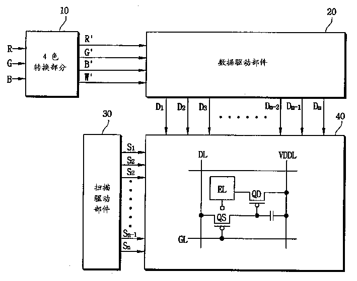
图3为本发明一个示范实施例OELD装置的原理示意图;Fig. 3 is the schematic diagram of the principle of OELD device of an exemplary embodiment of the present invention;
图4为表示根据本发明一个实施例的图3中四色转换部件的原理示意图;FIG. 4 is a schematic diagram showing the principle of the four-color conversion component in FIG. 3 according to an embodiment of the present invention;
图5A与5B的曲线图用于描述白色分量的提取;The graphs of Figures 5A and 5B are used to describe the extraction of the white component;
图6为表示根据本发明另一实施例的图3中四色转换部件原理示意图;FIG. 6 is a schematic diagram showing the principle of the four-color conversion component in FIG. 3 according to another embodiment of the present invention;
图7为与灰度数据相关的灰度系数的特性曲线;Fig. 7 is the characteristic curve of the gamma factor relevant to the grayscale data;
图8A至8C为本发明OELD装置的各像素配置示意图;8A to 8C are schematic diagrams of pixel configurations of the OELD device of the present invention;
图9为根据本发明的示范实施例的OELD装置的横断面图;9 is a cross-sectional view of an OELD device according to an exemplary embodiment of the present invention;
图10为根据本发明的另一示范实施例的OELD装置的横断面图;10 is a cross-sectional view of an OELD device according to another exemplary embodiment of the present invention;
图11为根据本发明的又一示范实施例的OELD装置的横断面图;11 is a cross-sectional view of an OELD device according to yet another exemplary embodiment of the present invention;
图12为根据本发明的又一示范实施例的OELD装置的横断面图。FIG. 12 is a cross-sectional view of an OELD device according to yet another exemplary embodiment of the present invention.
具体实施方式Detailed ways
本发明的说明性的实施例详细公开如下。然而,以下详细公开的具体结构及功能仅用于说明本发明的典型实施例。以下结合附图对实施例的描述中,对相同的或等效部件采用相同的标号。Illustrative embodiments of the present invention are disclosed in detail below. However, the specific structures and functions disclosed in detail below are only for illustrating typical embodiments of the present invention. In the following description of the embodiments in conjunction with the drawings, the same or equivalent components are given the same reference numerals.
通常,一旦液晶显示(LCD)装置中背光亮度及滤色片类型确定后,LCD装置的R.·G·.B色彩中的每一个都有预定的亮度,因此要增加亮度是困难或不可能的。与之对比,在有机场致发光显示(OELD)装置中,通过控制各个R·G·B色彩的电压数据可以增大R·G·B色彩中每一个的亮度。Usually, once the backlight brightness and color filter type are determined in a liquid crystal display (LCD) device, each of the R.·G·..B colors of the LCD device has a predetermined brightness, so it is difficult or impossible to increase the brightness of. In contrast, in an organic electroluminescence display (OELD) device, the luminance of each of the R·G·B colors can be increased by controlling the voltage data of the respective R·G·B colors.
在LCD装置中,当LCD装置亮度增加时,LCD装置的发光效率(即透光率)增加。与之对比,在OELD装置中,发光效率与亮度没有这样的关系。换句话说,在OELD装置中,当通过控制数据电压(data voltage)使一个更大的电流流过像素电极时,OELD装置的亮度增加但它的发光效率不提高。为了减少OELD的功率损耗,应该提高它的发光效率。根据本发明,OELD装置的发光效率及亮度均得到提高。下面将对此进行详细描述。In the LCD device, when the brightness of the LCD device increases, the luminous efficiency (ie, light transmittance) of the LCD device increases. In contrast, in OELD devices, there is no such relationship between luminous efficiency and luminance. In other words, in the OELD device, when a larger current flows through the pixel electrode by controlling the data voltage, the luminance of the OELD device increases but its luminous efficiency does not increase. In order to reduce the power loss of the OELD, its luminous efficiency should be improved. According to the present invention, both the luminous efficiency and brightness of the OELD device are improved. This will be described in detail below.
一种OELD,特别是有源基体OELD(AMOELD),包括一种有多层有机薄膜的发光叠层。有机薄膜配置在第一电极(例如阳极)与第二电极(例如阴极)之间,而第一电极由透明材料例如铟锡氧化物(ITO)组成;第二电极由低逸出功金属组成。当将直流电流施加到第一电极与第二电极时,来自第一电极的空穴及来自第二电极的电子注入有机发光层,并在那里复合。这样OELD装置就发出光线。An OELD, in particular an active matrix OELD (AMOELD), comprises a light emitting stack with multiple organic thin films. The organic thin film is arranged between the first electrode (such as anode) and the second electrode (such as cathode), and the first electrode is made of transparent material such as indium tin oxide (ITO); the second electrode is made of low work function metal. When a direct current is applied to the first electrode and the second electrode, holes from the first electrode and electrons from the second electrode are injected into the organic light emitting layer and recombine there. The OELD device thus emits light.
图2是用于说明利用根据本发明的实施例的OELD装置色彩显示的曲线图。与图1所示的常规LCD装置的色彩显示比较,其中的亮度在六边形区域(O、R、R’G、R’G’、RG’、G)内定标(scale);而本发明的OELD装置的色彩亮度显示是在扩展了灰度区(R、R’、R’G及G、RG’、G’)的矩形区域(O、R、R’、R’G’、RG’、G’、G)内定标。这是由于本发明的OELD装置中使用了较高的比例系数S。FIG. 2 is a graph for explaining color display using an OELD device according to an embodiment of the present invention. Compared with the color display of the conventional LCD device shown in Fig. 1, the brightness therein is scaled (scale) in the hexagonal area (O, R, R'G, R'G', RG', G); and the present invention The color brightness display of the OELD device is in the rectangular area (O, R, R', R'G', RG') of the extended gray area (R, R', R'G and G, RG', G'). , G', G) internal calibration. This is due to the higher scaling factor S used in the OELD device of the present invention.
在OELD装置中,从RGB色彩的原始灰度数据中提取白色(W)的灰度数据,并通过利用提取的W灰度数据及原始RGB灰度数据得到经补偿的RGBW灰度数据。此处原始RGB灰度数据是外部提供的,而经补偿的RGBW灰度数据是用于四种色彩的数据。这样,OELD装置亮度按与比例系数S相同的倍数得到提高,OELD装置的发光效率也就得到提高。In the OELD device, grayscale data of white (W) is extracted from original grayscale data of RGB colors, and compensated RGBW grayscale data is obtained by using the extracted W grayscale data and the original RGB grayscale data. Here, the original RGB grayscale data is provided externally, and the compensated RGBW grayscale data is data for four colors. In this way, the brightness of the OELD device is increased by the same multiple as the proportional coefficient S, and the luminous efficiency of the OELD device is also improved.
再次参见图1,如在六边形区域(O、R、R’G、R’G’、RG’、G)中限定一特定色彩,可以将原始RGB灰度数据转换为RGBW灰度数据,RGBW灰度数据用于表示这一特定色彩的灰度。然而,如果在三角形区域(R、R’、R’G、或G、G’、RG’)中限定某一色彩,由原始RGB数据转换的RGBW灰度数据就超出常规LCD装置及四色显示方法的可能达到的灰度范围。Referring to Figure 1 again, if a specific color is defined in the hexagonal area (O, R, R'G, R'G', RG', G), the original RGB grayscale data can be converted into RGBW grayscale data, RGBW grayscale data is used to represent the grayscale of this particular color. However, if a certain color is defined in the triangular area (R, R', R'G, or G, G', RG'), the RGBW grayscale data converted from the original RGB data exceeds the conventional LCD device and four-color display. The possible grayscale range of the method.
与之对照,本发明的OELD装置,使用一个数据驱动装置,其可以使在三角形区域和六边形区域内限定的各色彩都要使用RGBW灰度数据来显示。该数据驱动装置具有的处理数据的能力比原始RGB灰度数据的容量更大。例如,当原始RGB灰度数据为6比特(bit)数据时,数据驱动装置可以处理7比特或8比特容量(size)的数据;因此,可以由该数据驱动装置处理比6比特RGB灰度数据更大的RGBW灰度数据。In contrast, the OELD device of the present invention uses a data driving device that enables each color defined in the triangular area and the hexagonal area to be displayed using RGBW grayscale data. The data driving device has a capability of processing data larger than the capacity of the original RGB grayscale data. For example, when the original RGB grayscale data is 6-bit (bit) data, the data drive device can process data with a capacity of 7 bits or 8 bits; Larger RGBW grayscale data.
参见图2,第一原始灰度数据I转换为第一经补偿的灰度数据I’,以显示第一色彩;第二原始灰度数据II转换为第二经补偿的灰度数据II’,以显示第二色彩。由于可以通过利用在已扩展灰度区中的第二经补偿的灰度数据II’显示第二色彩,所以第二色彩的亮度就可以比使用第二原始灰度II显示的色彩更亮(与比例系数S有同样的倍数)。Referring to FIG. 2, the first original grayscale data I is converted into the first compensated grayscale data I' to display the first color; the second original grayscale data II is converted into the second compensated grayscale data II', to display the secondary color. Since the second color can be displayed by using the second compensated gradation data II' in the extended gradation area, the brightness of the second color can be brighter than the color displayed using the second original gradation II (with the Scale factor S has the same multiple).
当原始RGB灰度数据转换为经补偿的RGBW灰度数据时,需确定比例系数,例如取1或更大。本实施例中,比例系数为2(将在以后详细说明)。When the original RGB grayscale data is converted into compensated RGBW grayscale data, a scaling factor needs to be determined, for example, 1 or greater. In this embodiment, the proportionality factor is 2 (details will be described later).
在本发明的OELD装置中,从原始RGB灰度数据中提取白色灰度数据,并且在原始RGB灰度数据中减去白色灰度数据,以得到新的RGB灰度数据。由新RGB数据及提取的白色灰度数据得到经补偿的RGBW灰度数据,即四色数据:红、绿、兰及白。当比例系数为“1”时,虽然通过附加白灰度数据使亮度没有或仅有少量增加,但提高了显示器的发光效率,降低了功率的消耗。通过控制数据电压可使亮度提高。In the OELD device of the present invention, white grayscale data is extracted from the original RGB grayscale data, and the white grayscale data is subtracted from the original RGB grayscale data to obtain new RGB grayscale data. Compensated RGBW grayscale data is obtained from the new RGB data and the extracted white grayscale data, that is, four-color data: red, green, blue and white. When the proportionality coefficient is "1", although the luminance is not or only slightly increased by adding white gray scale data, the luminous efficiency of the display is improved and the power consumption is reduced. Brightness can be improved by controlling the data voltage.
图3为根据本发明一个实施例的OELD装置的原理示意图。该OELD装置包括:一个四色转换部件10;一个数据驱动部件20;一个扫描驱动部件30;一个OELD板40。FIG. 3 is a schematic diagram of the principle of an OELD device according to an embodiment of the present invention. The OELD device includes: a four-
四色转换部件10将原始RGB灰度数据R、G、B转换为RGBW补偿数据R’、G’、B’、W’并提供给数据驱动部件20。原始RGB灰度数据R、G、B由外部,例如外部主机或图形控制器(未示出)提供。通过附加白色灰度数据得到经补偿的RGBW灰度数据R’、G’、B’、W’,以增加亮度。The four-
数据驱动部件20处理来自四色转换部件10的经补偿的RGBW灰度数据R’、G’、B’、W’,以产生模拟类型数据信号D1,D2,......Dm。OELD板40接收所述数据信号并根据这些数据信号显示色彩。扫描驱动部件30向OELD板40顺序提供多个扫描信号S1,S2,......Sn。The data driving part 20 processes the compensated RGBW grayscale data R', G', B', W' from the four-
OELD板40包括:以矩阵形式配置的多个数据线DL,多个扫描线GL及多个电源线VDDL。数据线DL传输数据信号D1,D2,......,Dm,扫描线GL传输扫描信号S1,S2,......,Sn,电源线VDDL传输外部提供的电功率。The OELD board 40 includes: a plurality of data lines DL, a plurality of scan lines GL and a plurality of power lines VDDL arranged in a matrix. The data lines DL transmit data signals D1, D2, . . . , Dm, the scan lines GL transmit scan signals S1, S2, .
OELD板40包括众多像素。每一个像素有一个开关元件QS;一个有机场致发光元件EL;驱动元件QD。开关元件QS有分别连接到数据线DL及扫描线GL的第一及第二端。开关元件QS还有一个第三端,响应于加到第二端上的扫描信号通过其输出一个来自数据线DL的数据信号。换句话说,由加到第二端上的扫描信号来转换来使用于传输数据信号的开关元件QS的传输通道通或断(on or off)。The OELD panel 40 includes numerous pixels. Each pixel has a switching element QS; an organic electroluminescent element EL; and a driving element QD. The switch element QS has first and second ends respectively connected to the data line DL and the scan line GL. The switching element QS also has a third terminal through which a data signal from the data line DL is output in response to the scan signal applied to the second terminal. In other words, the transmission channel of the switching element QS for transmitting the data signal is switched on or off by the scan signal applied to the second terminal.
有机场致发光元件EL有一个连接极性端的第一端及一个接收电流信号的第二端。响应于由第二端提供的电流信号的量值,有机场致发光元件EL发出光线的亮度变化。The organic electroluminescent element EL has a first end connected to the polarity end and a second end receiving a current signal. In response to the magnitude of the current signal provided by the second terminal, the brightness of the light emitted by the organic electroluminescence element EL changes.
驱动元件QD有一个连接到有机场致发光元件EL第二端的第一端及一个连接到电源线VDDL的第二端。驱动元件QD也有一个连接到开关元件第三端的第三端。驱动元件有一个从第二端到第一端形成的传输通道,通过它使来自电源线VDDL的电流流向有机场致发光元件EL。响应于由开关元件QS的第三端提供的数据信号,控制(即通断)驱动元件QD的传输通道。通过控制通过驱动元件QD的传输通道提供给有机场致发光元件EL的电流,可以控制有机场致发光元件EL发出的光线的亮度。The driving element QD has a first terminal connected to the second terminal of the organic electroluminescent element EL and a second terminal connected to the power line VDDL. The driving element QD also has a third terminal connected to the third terminal of the switching element. The driving element has a transmission channel formed from the second terminal to the first terminal, through which the current from the power supply line VDDL flows to the organic electroluminescent element EL. In response to the data signal provided by the third terminal of the switching element QS, the transmission channel of the driving element QD is controlled (ie switched on and off). By controlling the current supplied to the organic electroluminescent element EL through the transmission channel of the driving element QD, the brightness of the light emitted by the organic electroluminescent element EL can be controlled.
OELD板40中的各像素,通过利用与红色光线、绿色光线、兰色光线、白色光线中相对应的一个,每个像素显示一种色彩,红、绿、兰、白中的一个。这些像素可以是有源发光型或滤色型。有源发光型的各像素的每一个由EL元件发出R光线、G光线、B光线或W光线,而滤色型的各像素的每一个通过R滤色片、G滤色片、B滤色片或W滤色片发出R光线、G光线、B光线或W光线。Each pixel in the OELD panel 40 displays a color, one of red, green, blue, and white, by using one corresponding to red light, green light, blue light, and white light. These pixels can be active-emissive or color-filtered. Each pixel of the active light-emitting type emits R light, G light, B light or W light from the EL element, and each pixel of the color filter type passes through the R color filter, G color filter, B color filter R light, G light, B light or W light are emitted by the filter or W filter.
图4为表示根据本发明的一个实施例的图3中四色转换部件的原理示意图。图4中四色转换部件10包括:一个灰度系数转换部件11;一个再变换部件12;一个白色提取部件13;一个数据确定部件14;一个逆灰度系数转换部件15。四色转换部件10接收原始RGB灰度数据并将它转换为四色RGB灰度数据。FIG. 4 is a schematic diagram showing the principle of the four-color conversion unit in FIG. 3 according to an embodiment of the present invention. The four-
详细地说,灰度系数转换部件11接收原始RGB灰度数据,并将它转换为经灰度转换的RGB数据。原始RGB数据的每个色彩数据转换为经灰度转换的RGB数据的每个色彩数据。如下列表达式1所示。In detail, the
表达式1
RY=a RY R Y =a R Y
GY=a GY G Y =a G Y
BY=a BY B Y =a B Y
式中,RY、GY及BY分别为R色彩、G色彩及B色彩相对于各色彩中对应的最大亮度的规一化亮度数据。此外,“a”表示(1/Gmax)Y,RY、GY及BY分别是对应于R色彩、G色彩及B色彩的灰度数值。Gmax表示最大灰度值。例如,当RGB数据的全灰度是64时,它的Gmax是63。In the formula, R Y , G Y and BY are the normalized brightness data of R color, G color and B color relative to the corresponding maximum brightness of each color. In addition, "a" represents (1/Gmax) Y , and R Y , G Y and B Y are grayscale values corresponding to R color, G color and B color, respectively. Gmax represents the maximum gray value. For example, when the full gray scale of RGB data is 64, its Gmax is 63.
再变换部件12接收经灰度系数转换的RGB数据,并对每个经灰度转换的RGB数据中的各色彩数据进行倍增及再变换。例如,再变换部件12以比例系数2倍增经灰度转换的RGB数据的每个色彩数据RY、GY、BY,如表达式2所示。再变换部件12然后向白色提取部件13及数据确定部件14提供经再变换的RGB数据。The
表达式2expression 2
RY’=SRY R Y '=SR Y
GY’=SGY G Y '=SG Y
BY’=SBY B Y '=SB Y
式中,S为比例系数,是从RGB色彩组合得到的白色光的最大亮度与从RGBW色彩组合得到的白色光的最大亮度的比。当使用滤色片时,比例系数S最好为2。In the formula, S is a proportional coefficient, which is the ratio of the maximum brightness of white light obtained from RGB color combination to the maximum brightness of white light obtained from RGBW color combination. When color filters are used, the scale factor S is preferably 2.
白色提取部件13接收经再变换的RGB数据并考虑到各自的色彩数据RY’、GY’、BY’从经再变换的RGB数据中提取白色分量。然后将白色分量提供给数据确定部件14。The
参见图5A,当经再变换的RGB数据中的各色彩数据RY’、GY’、BY’的最小亮度等于或大于预定值时,以aGmaxY为例,预定值aGmaxY就变成白色分量WY’,并提供给数据确定部件14。本例中,兰色数据最小亮度BY’比预定值aGmaxY大。Referring to Fig. 5A, when the minimum brightness of each color data RY ' , G Y ', BY ' in the reconverted RGB data is equal to or greater than a predetermined value, taking aGmax Y as an example, the predetermined value aGmax Y becomes The white component W Y ' is provided to the
参见图5B,当经再变换的RGB数据中的各色彩数据RY’、GY’、BY’的最小亮度小于aGmaxY时,色彩数据RY’、GY’、BY’的最小亮度变成白色分量WY’,并提供给数据确定部件14。本例中,兰色数据最小亮度BY’比预定值aGmaxY小。这样,白色分量提取可以用表达式3示出。Referring to Fig. 5B, when the minimum brightness of each color data RY ' , G Y ', BY ' in the re-transformed RGB data is less than aGmax Y , the minimum brightness of the color data RY ' , G Y ', BY ' The luminance becomes a white component W Y ′, and is supplied to the
表达式3expression 3
WY’=aGmaxY,如Min[RY’、GY’、BY’]aGmaxY W Y '=aGmax Y , such as Min[R Y ', G Y ', B Y '] aGmax Y
WY’=Min[RY’、GY’、BY’],如Min[RY’、GY’、BY’]<aGmaxY W Y '=Min[R Y ', G Y ', B Y '], such as Min[R Y ', G Y ', B Y ']<aGmax Y
数据确定部件14接收来自再变换部件12的经再变换的RGB数据及来自白色提取部件13的白色分量,并在这些输入数据的基础上确定新的RGBW数据(RY *、GY *、BY *、WY *)。该新RGBW数据的每个色彩数据是通过由经再变换的RGB数据中对应的色彩数据减去白色分量得到的,见下列表达式4。然后将新RGBW数据提供给逆灰度系数转换部件15。The
表达式4expression 4
RY *=RY’-WY’R Y * = R Y '-W Y '
GY *=GY’-WY’G Y * = G Y '-W Y '
BY *=BY’-WY’B Y * =B Y '-W Y '
WY *=WY’W Y * = W Y '
逆灰度系数转换部件15执行对于来自数据确定部件14的新RGBW数据中的对应色彩数据RY *、GY *、BY *、WY *的逆灰度系数转换,以产生经逆灰度系数转换的RGBW灰度数据RY *、GY *、BY *、WY *。下列表达式5示出逆灰度系数转换部件15所执行的逆灰度系数转换。经补偿的RGBW灰度数据提供给数据驱动部件20(见图3)。The inverse
表达式5expression 5
R’=(RY*/a)1/Y R'=(RY * /a) 1/Y
G’=(GY */a)1/Y G'=(G Y * /a) 1/Y
B’=(BY */a)1/Y B'=(B Y * /a) 1/Y
W’=(WY */a)1/Y W'=(W Y * /a) 1/Y
为了使一种色彩,例如图2曲线图中扩展灰度区的一种原色显示出更好的色彩纯度,经四色转换的RGBW数据(R’、G’、B’、W’)中的色彩数据灰度可以比最大灰度值(Gmax)更大,以便超过灰度定标所能显示的最大亮度。然而,由于本发明扩展了灰度,利用数据驱动IC就能显示出超过最大亮度的色彩数据。本发明中,数据驱动IC可以处理比原始RGB灰度数据更大比特容量的数据。为此,数据驱动部件20可以由多个数据驱动装置实现。In order to make a color, such as a primary color in the extended gray-scale area in the graph of Figure 2, show better color purity, the four-color converted RGBW data (R', G', B', W') The color data grayscale can be larger than the maximum grayscale value (Gmax) in order to exceed the maximum brightness that can be displayed by grayscale scaling. However, since the present invention extends the gray scale, color data exceeding the maximum luminance can be displayed using the data driver IC. In the present invention, the data driver IC can process data with a larger bit capacity than the original RGB grayscale data. To this end, the data driving part 20 may be realized by a plurality of data driving devices.
虽然白色提取部件13通过将经再变换的RGB数据的最小亮度与所述实施例中的预定值aGmaxY进行比较提取白色分量,但经再变换的RGB数据中对应色彩数据的最小亮度仍可以不需比较过程来确定,并作为提取的白色分量提供给数据确定部件14。换句话说,从经再变换的RGB数据中的各自色彩数据可提取白色分量,而不需确定预定值aGmaxY。利用除最小亮度的色彩数据以外的对应色彩数据与白色分量之间的差,来确定除按照白色分量确定的最小亮度色彩数据以外的色彩数据。Although the white extracting
在图4的实施例中,按比例系数为2倍增经灰度系数转换的RGB灰度数据以便将灰度扩展为2倍,用于提取白色分量以产生新RGBW灰度数据。在这种情况下,需要扩展数据驱动IC的比特容量,例如,灰度为64时,虽然6比特容量数据驱动IC是适当的,但是在灰度扩展到70或80灰度时,还是应该使用7比特容量的数据驱动IC。为避免增加数据驱动IC的比特容量,可以在不乘以比例系数的情况下处理色彩数据。下面将详细描述这样的实施例。In the embodiment of FIG. 4 , the gamma-converted RGB grayscale data is multiplied by a factor of 2 to expand the grayscale by a factor of 2 for extracting white components to generate new RGBW grayscale data. In this case, it is necessary to expand the bit capacity of the data driver IC. For example, when the grayscale is 64, although a 6-bit capacity data driver IC is appropriate, it should be used when the grayscale is extended to 70 or 80 grayscale. 7-bit capacity data driver IC. To avoid increasing the bit capacity of the data driver IC, the color data can be processed without multiplying by the scaling factor. Such an embodiment will be described in detail below.
图6为根据本发明另一实施例四色转换部件原理示意图。图6中四色转换部件10’包括:一个灰度系数转换部件16;一个白色提取部件17;一个数据确定部件18;一个逆灰度系数转换部件19。四色转换部件10’将原始RGB灰度数据转换为四色RGBW灰度数据。Fig. 6 is a schematic diagram of the principle of a four-color conversion component according to another embodiment of the present invention. The four-color conversion unit 10' in Fig. 6 includes: a
灰度系数转换部件16接收原始RGB数据并将原始RGB数据的每个色彩数据转换为经灰度系数转换的RGB数据RY,GY,BY的每个色彩数据,如以下表达式6所示。然后将经灰度系数转换的RGB数据RY,GY,BY提供给白色提取部件17及数据确定部件18。The
表达式6expression 6
RY=a RY R Y =a R Y
GY=a GY G Y =a G Y
BY=a BY B Y =a B Y
每个经灰度系数转换的RGB数据的每个色彩数据RY,GY,BY是相对于它的最大亮度规一化的、原始RGB数据中与色彩数据R、G、B对应的亮度数据。上述表达式6中,a等于(1/Gmax)Y,Gmax为最大灰度值。例如,当全灰度为64时,Gmax为63,且灰度数(number)在0与63之间。此外,“RY”、“GY”、“BY”分别为对应RGB色彩的灰度数。Each color data R Y , G Y , and BY of each gamma-converted RGB data is the brightness corresponding to the color data R, G, and B in the original RGB data normalized with respect to its maximum brightness data. In the above expression 6, a is equal to (1/Gmax) Y , and Gmax is the maximum gray value. For example, when the full grayscale is 64, Gmax is 63, and the grayscale number (number) is between 0 and 63. In addition, “ RY ”, “G Y ”, and “B Y ” are the grayscale numbers corresponding to the RGB colors, respectively.
白色提取部件17接收经灰度系数转换的RGB数据RY、GY、BY,并从经灰度系数转换的RGB数据中提取白色分量。然后将该提取的白色分量提供给数据确定部件18。例如,当全灰度为64时,对应于全灰度的半亮度的灰度是46灰度(不是32灰度),如图7所示。此时白色分量可由下列表达式7确定。The
表达式7expression 7
WY=a·46Y,如Min[RY,GY,BY]≥a·46Y W Y =a·46 Y , such as M in [R Y , G Y , B Y ]≥a·46 Y
WY=Min[RY,GY,BY],如Min[RY,GY,BY]]<a·46Y W Y =M in [R Y , G Y , B Y ], such as M in [R Y , G Y , B Y ]]<a·46 Y
在另一例中,白色分量可以按照经灰度系数转换的RGB数据中的各色彩数据RY、GY、BY的最小数据确定,如下列表达式8所示。In another example, the white component may be determined according to the minimum data of each color data RY , GY , BY in the gamma-converted RGB data, as shown in Expression 8 below.
表达式8expression 8
WY=Min[RY、GY、BY]W Y = M in [R Y , G Y , B Y ]
然后将白色分量WY提供给数据确定部件18,数据确定部件18还接收来自灰度系数转换部件16的经灰度系数转换的RGB数据。数据确定部件18根据经灰度系数转换的RGB数据的对应色彩数据和白色分量确定新RGBW数据的每个色彩数据RY”、GY”、WY”,如下列表达式9示出。The white component W Y is then supplied to the
表达式9expression 9
RY”=RY-WY R Y "=R Y -W Y
GY”=GY-WY G Y ”=G Y -W Y
BY”=BY-WY B Y "=B Y -W Y
WY”=WY W Y ”=W Y
然后将由数据确定部件18得出的新RGBW数据RY”、GY”、BY”、WY”提供给反向灰度系数补偿部件19。反向灰度系数补偿部件19转换RGBW数据的每个色彩数据RY”、GY”、BY”、WY”以产生对应的RGBW逆灰度系数转换的灰度数据的色彩数据R’、G’、B’、W’。如下列表达式10所示。The new RGBW data R Y ″, G Y ″, BY ″ , W Y ″ derived from the
表达式10
R’=(RY”/a)1/Y R'=(R Y ”/a) 1/Y
G’=(GY”/a)1/Y G'=(G Y ”/a) 1/Y
B’=(BY”/a)1/Y B'=(B Y ”/a) 1/Y
W’=(WY”/a)1/Y W'=(W Y ”/a) 1/Y
然后将经逆灰度系数转换的RGBW数据R’、G’、B’、W’提供给数据驱动部件20(参见图3)。The inverse gamma-converted RGBW data R', G', B', W' are then supplied to the data driving section 20 (see FIG. 3).
本实施例中,白色提取部件17通过将经灰度系数转换的RGB数据中的各自色彩数据RY、GY、BY的最小亮度与预定值(例如在全灰度为64的情况下)进行比较,以提取白色分量并将提取的白色分量提供给数据确定部件14。然而,白色分量也可通过限定经灰度系数转换的RGB数据中的各自色彩数据RY、GY、BY的最小亮度提取(参见图5B)。In this embodiment, the
本发明OELD装置中各像素的配置说明如下。本发明OELD装置中用于显示四色像素的配置的例子如图8A-8C所示。参见图8A,OELD装置的一个像素包括四个子像素:一个红色子像素R,一个绿色子像素G,一个兰色子像素B,一个白色子像素W。各子像素呈条状并互相平行配置,组成一个像素。由于该像素包含所述白色子像素,增加了OELD装置的亮度。The arrangement of each pixel in the OELD device of the present invention is explained as follows. An example of the arrangement of pixels for displaying four colors in the OELD device of the present invention is shown in FIGS. 8A-8C . Referring to FIG. 8A , one pixel of the OELD device includes four sub-pixels: a red sub-pixel R, a green sub-pixel G, a blue sub-pixel B, and a white sub-pixel W. Each sub-pixel is striped and arranged parallel to each other to form a pixel. Since the pixel contains the white sub-pixel, the brightness of the OELD device is increased.
虽然图8A中各子像素的大小基本上是相同的,但这些子像素的大小可以不一样。在这种情况下,开关晶体管,数据线与/或选通线可以有与具有不同大小的子像素间隔对应的不同的间隔。然而,开关晶体管,数据线与/或选通线的间隔与那些大小基本相同的子像素的间隔可保持基本相同。Although the sizes of the sub-pixels in FIG. 8A are substantially the same, the sizes of the sub-pixels may be different. In this case, switching transistors, data lines and/or gate lines may have different intervals corresponding to sub-pixel intervals having different sizes. However, the spacing of switching transistors, data lines and/or gate lines may remain substantially the same as those of sub-pixels of substantially the same size.
参见图8B,OELD装置的一个像素包括:一个红色子像素R;一个绿色子像素G;一个兰色子像素B;一个白色子像素W,它们配置在一个2*2的网格中。Referring to FIG. 8B , a pixel of the OELD device includes: a red sub-pixel R; a green sub-pixel G; a blue sub-pixel B; and a white sub-pixel W, which are arranged in a 2*2 grid.
参见图8C,OELD装置的一个像素包括:两个红色子像素R1、R2;两个绿色子像素G1、G2;一个兰色子像素B;一个白色子像素W,它们配置在一个2*3的网格中。正如图8C所示,所述两个红色子像素R1、R2是分开配置的,两个绿色子像素G1、G2也互相分开配置。然而,在另一实施例中,两个红色子像素R1、R2可以互相靠近,两个绿色子像素G1、G2也可作同样方式配置。Referring to Fig. 8C, a pixel of the OELD device includes: two red sub-pixels R1, R2; two green sub-pixels G1, G2; one blue sub-pixel B; one white sub-pixel W, which are arranged in a 2*3 grid. As shown in FIG. 8C , the two red sub-pixels R1 and R2 are arranged separately, and the two green sub-pixels G1 and G2 are also arranged separately. However, in another embodiment, the two red sub-pixels R1, R2 can be close to each other, and the two green sub-pixels G1, G2 can also be configured in the same way.
以下详述本发明OELD装置中的OELD板的几个不同实施例。Several different embodiments of the OELD plate in the OELD device of the present invention are described in detail below.
图9为本发明实施例OELD板剖面图。参见图9,一个绝缘层110是在透明基片105上形成的。透明基片105可由玻璃、石英、玻璃陶瓷、水晶玻璃或它们的组合构成。透明基片105最好选用耐热材料。Fig. 9 is a sectional view of an OELD board according to an embodiment of the present invention. Referring to FIG. 9, an insulating layer 110 is formed on the transparent substrate 105. Referring to FIG. The transparent substrate 105 can be made of glass, quartz, glass ceramics, crystal glass or combinations thereof. The transparent substrate 105 is preferably made of a heat-resistant material.
在使用石英基片时可以省去绝缘层110,绝缘层110可由包括例如硅在内的材料构成。硅绝缘层110可包括氧、氮或它们的混合物。例如,硅绝缘层110可以是一种氧化硅层,一种氮化硅层或一种氮氧化硅层(SiOxNy,这里x及y为整数)。The insulating layer 110 can be omitted when a quartz substrate is used, and the insulating layer 110 can be composed of a material including, for example, silicon. The silicon insulating layer 110 may include oxygen, nitrogen, or a mixture thereof. For example, the silicon insulating layer 110 may be a silicon oxide layer, a silicon nitride layer or a silicon oxynitride layer (SiOxNy, where x and y are integers).
在绝缘层110上形成多个电流控制晶体管,它们中的每一个包括:一个激励(active)层;一个栅极绝缘层120;一个栅极125;一个第一绝缘夹层127;一个源极130;一个漏极135。激励层包括:一个源极区112;一个沟道区114;一个漏极区116。栅极绝缘层120在激励层上形成,以显露出源极区112及漏极区116。栅极125形成在栅极绝缘层120。第一绝缘夹层127形成在栅极125及栅极绝缘层120上,以显露出源极区112及漏极区116。特别是,第一绝缘夹层127上有一些分别与栅极绝缘层120连接孔基本相同位置上形成的连接孔,因此源极区112及漏极区116通过与栅极绝缘层120及第一绝缘夹层127中对应的连接孔部分显露出。形成在第一绝缘夹层127上的源极130通过与栅极绝缘层120及第一绝缘夹层127上的对应连接孔显露出的源极区112相连。形成在第一绝缘夹层127上的漏极135通过与栅极绝缘层120及第一绝缘夹层127上对应连接孔显露出的漏极区116相连。A plurality of current control transistors are formed on the insulating layer 110, each of them comprising: an excitation (active) layer; a gate insulating layer 120; a gate 125; a first insulating interlayer 127; a source 130; A drain 135 . The excitation layer includes: a source region 112 ; a channel region 114 ; and a drain region 116 . A gate insulating layer 120 is formed on the active layer to expose the source region 112 and the drain region 116 . The gate electrode 125 is formed on the gate insulating layer 120 . A first insulating interlayer 127 is formed on the gate 125 and the gate insulating layer 120 to expose the source region 112 and the drain region 116 . In particular, some connection holes are formed on the first insulating interlayer 127 at substantially the same positions as the connection holes of the gate insulating layer 120, so the source region 112 and the drain region 116 are connected to the gate insulating layer 120 and the first insulating layer 120. The corresponding connection holes in the interlayer 127 are partially exposed. The source electrode 130 formed on the first insulating interlayer 127 is connected to the gate insulating layer 120 and the source region 112 exposed by the corresponding connection hole on the first insulating interlayer 127 . The drain 135 formed on the first insulating interlayer 127 is connected to the gate insulating layer 120 and the drain region 116 exposed by corresponding connection holes on the first insulating interlayer 127 .
虽然图9中的栅极125只是单层结构,但在不同的实施例中栅极也可以是多层结构。源极130与在第一方向延伸的源极线相连,漏极135与在不同于第一方向的第二方向延伸的漏极线相连。电流控制晶体管的栅极125通过漏极线与开关晶体管(未示出)的漏极区相连。源极线与电源线(未示出)相连。Although the gate 125 in FIG. 9 is only a single-layer structure, the gate may also be a multi-layer structure in different embodiments. The source electrode 130 is connected to a source line extending in a first direction, and the drain electrode 135 is connected to a drain line extending in a second direction different from the first direction. The gate 125 of the current control transistor is connected to the drain region of the switching transistor (not shown) through a drain line. The source line is connected to a power line (not shown).
第二绝缘夹层140形成在第一绝缘夹层127及源极130、漏极135上,并在与漏极135对应的位置上有连接孔。因此每个漏极135都通过第二绝缘夹层140上对应的一个连接孔显露。第二绝缘夹层140上的各连接孔都与第一绝缘夹层127上对应的连接孔对准。The second insulating interlayer 140 is formed on the first insulating interlayer 127 , the source 130 , and the drain 135 , and has a connection hole at a position corresponding to the drain 135 . Therefore, each drain electrode 135 is exposed through a corresponding connection hole on the second insulating interlayer 140 . Each connecting hole on the second insulating interlayer 140 is aligned with the corresponding connecting hole on the first insulating interlayer 127 .
像素电极145形成在第二绝缘夹层140的每个连接孔,其通过第二绝缘夹层140上对应的连接孔与对应的漏极135相连。具体地说,像素电极145上有一连接部分,通过第二绝缘夹层140上对应的连接孔其由第二绝缘夹层140上形成的像素电极145的一部分延伸到对应的漏极135。像素电极可由例如导电的氧化物形成。A pixel electrode 145 is formed in each connection hole of the second insulating interlayer 140 , and is connected to the corresponding drain electrode 135 through the corresponding connection hole on the second insulating interlayer 140 . Specifically, there is a connecting portion on the pixel electrode 145 , which extends from a part of the pixel electrode 145 formed on the second insulating interlayer 140 to the corresponding drain electrode 135 through the corresponding connecting hole on the second insulating interlayer 140 . The pixel electrode may be formed of, for example, conductive oxide.
在第二绝缘夹层140及像素电极145上形成间隔层(patition wall)150,用以限定OELD装置中的各发光区。用间隔层150限定分别与红色、绿色、兰色、白色像素对应的红色发光区、绿色发光区、兰色发光区、白色发光区。在这些像素电极145及间隔层150上形成有机EL层,这样,分别在用间隔层150限定的各红色、绿色、兰色、白色发光区形成红色有机EL层16R、绿色有机EL层16G、兰色有机EL层16B、白色有机EL层16W。这样红色、绿色、兰色、白色有机EL层16R、16G、16B、16W分别发出红色、绿色、兰色、白色光线。虽然本实施例中红色、绿色、兰色、白色有机EL层16R、16G、16B、16W均为单一层结构,但在其它实施例中,有机EL层也可以是多层结构。例如,有机EL层可以为多层结构,包括:一个空穴注入层;一个空穴输送层;一个发光层及一个电子输送层,它们层叠在像素电极及间隔层上。此外,有机EL层也可以为如下多层结构,包括:一个空穴输送层;一个发光层及一个电子输送层,或一个多层结构,包括:一个空穴注入层;一个空穴输送层;一个发光层;一个电子输送层及一个电子注入层。A patition wall 150 is formed on the second insulating interlayer 140 and the pixel electrode 145 to define each light emitting area in the OELD device. The spacer layer 150 is used to define red light emitting regions, green light emitting regions, blue light emitting regions and white light emitting regions respectively corresponding to red, green, blue and white pixels. Organic EL layers are formed on these pixel electrodes 145 and spacers 150, so that red organic EL layers 16R, green organic EL layers 16G, blue organic EL layers 16R, color organic EL layer 16B and white organic EL layer 16W. In this way, the red, green, blue, and white organic EL layers 16R, 16G, 16B, and 16W respectively emit red, green, blue, and white light. Although the red, green, blue, and white organic EL layers 16R, 16G, 16B, and 16W in this embodiment all have a single-layer structure, in other embodiments, the organic EL layers may also have a multi-layer structure. For example, the organic EL layer can be a multilayer structure, including: a hole injection layer; a hole transport layer; a light emitting layer and an electron transport layer, which are stacked on the pixel electrodes and the spacer layer. In addition, the organic EL layer can also be the following multilayer structure, including: a hole transport layer; a light emitting layer and an electron transport layer, or a multilayer structure, including: a hole injection layer; a hole transport layer; A light emitting layer; an electron transport layer and an electron injection layer.
在有机EL层16R、16G、16B、16W上形成一个金属电极170。金属电极170可作为有机EL层的阴极,也可对有机EL层16R、16G、16B、16W形成保护。虽然图9所示的实施例中金属电极170作为阴极是在有机EL层上形成的,但是低逸出功材料,如镁(Mg)、锂(Li)、钙(Ca)或它们的混化物也可以作为阴极在有机EL层上形成。A metal electrode 170 is formed on the organic EL layers 16R, 16G, 16B, 16W. The metal electrode 170 can serve as a cathode of the organic EL layer, and can also protect the organic EL layers 16R, 16G, 16B, and 16W. Although the metal electrode 170 is formed on the organic EL layer as the cathode in the embodiment shown in FIG. 9, low work function materials such as magnesium (Mg), lithium (Li), calcium (Ca) or their mixture It can also be formed as a cathode on the organic EL layer.
由于本发明的OELD装置具有的白色像素发出白色光,另外红色、绿色、兰色象分别发出红色、绿色、兰色光,这样就提高了OELD装置的亮度、提高了发光效率,因此也就减小了OELD装置的功率消耗。以上参照图9描述的OELD装置为底部型,其中金属电极170作为阴极是在有机EL层上形成的,因此红色、绿色、兰色、白色光线由金属电极170反射,并通过基片105发出。以下将描述顶部发光型OELD装置。Because the white pixels that the OELD device of the present invention has emit white light, and the red, green, and blue color images emit red, green, and blue colors respectively, in addition, the brightness of the OELD device has been improved, and the luminous efficiency has been improved. The power consumption of the OELD device is reduced. The OELD device described above with reference to FIG. 9 is a bottom type, wherein a metal electrode 170 is formed on the organic EL layer as a cathode, so red, green, blue, and white light rays are reflected by the metal electrode 170 and emitted through the substrate 105. A top emission type OELD device will be described below.
图10为本发明另一实施例OELD板横断面图。图10的OELD板中,一个绝缘层210形成在基片205上,电流控制晶体管形成在绝缘层210。每个电流控制晶体管包括:一个激励层;一个栅极绝缘层220;一个栅极225;一个第一绝缘夹层227;一个源极230;一个漏极235。激励层包括:一个源极区212;一个沟道区214;一个漏极区216。栅极绝缘层220形成在激励层上并具有连接孔,以显露出源极区212及漏极区216。栅极225形成在栅极绝缘层220上。第一绝缘夹层227形成在栅极225及栅极绝缘层220并具有连接孔,以显露出源极区212及漏极区216。栅极225形成在栅极绝缘层220上。第一绝缘夹层227形成在栅极225及栅极绝缘层220上,并具有连接孔,以显露出源极区212及漏极区216。源极230及漏极235形成在第一绝缘夹层227上,分别与源极区及漏极区相连。Fig. 10 is a cross-sectional view of an OELD plate according to another embodiment of the present invention. In the OELD panel of FIG. 10, an insulating layer 210 is formed on a substrate 205, and a current control transistor is formed on the insulating layer 210. Referring to FIG. Each current control transistor includes: an excitation layer; a gate insulating layer 220 ; a gate 225 ; a first insulating interlayer 227 ; a source 230 ; The excitation layer includes: a source region 212 ; a channel region 214 ; and a drain region 216 . The gate insulating layer 220 is formed on the active layer and has connection holes to expose the source region 212 and the drain region 216 . The gate electrode 225 is formed on the gate insulating layer 220 . The first insulating interlayer 227 is formed on the gate 225 and the gate insulating layer 220 and has connection holes to expose the source region 212 and the drain region 216 . The gate electrode 225 is formed on the gate insulating layer 220 . The first insulating interlayer 227 is formed on the gate 225 and the gate insulating layer 220 , and has connection holes to expose the source region 212 and the drain region 216 . The source 230 and the drain 235 are formed on the first insulating interlayer 227 and connected to the source region and the drain region respectively.
第二绝缘夹层240形成在第一绝缘夹层227上并具有连接孔,以接纳源极或漏极的一部分。源极和漏极230、235分别与源极线和漏极线相连。一个平面(planarizing)层242形成在第二绝缘夹层240及源极和漏极230、235上。平面层242具有连接孔,它们与对应的漏极135(译注:疑为235)对准。The second insulating interlayer 240 is formed on the first insulating interlayer 227 and has a connection hole to receive a portion of the source or the drain. The source and drain electrodes 230, 235 are connected to source and drain lines, respectively. A planarizing layer 242 is formed on the second insulating interlayer 240 and the source and drain electrodes 230 , 235 . The planar layer 242 has connection holes, which are aligned with the corresponding drain electrodes 135 (Annotation: Suspected 235).
像素电极245形成在平面层242,其可由例如导电的氧化物形成。它们中的每一个通过在平面层242上形成的对应连接孔与对应的漏极235相连。间隔层250形成在平面层及像素电极245并用以限定发光区。相邻的各间隔层250确定对应于红色、绿色、兰色、白色像素的发光区。The pixel electrode 245 is formed on the planar layer 242, which may be formed of, for example, conductive oxide. Each of them is connected to a corresponding drain electrode 235 through a corresponding connection hole formed on the planar layer 242 . The spacer layer 250 is formed on the planar layer and the pixel electrode 245 to define the light emitting area. Adjacent spacer layers 250 define light emitting regions corresponding to red, green, blue and white pixels.
红色有机EL层26R、绿色有机EL层26G、兰色有机EL层26B、白色有机EL层26W形成在间隔层250及像素电极245上。红色、绿色、兰色、白色有机EL层分别由红色、绿色、兰色、白色像素区限定并发出红色、绿色、兰色、白色光线。虽然本实施例中有机EL层均为单一层结构,但在其他实施例中,有机EL层也可以是多层结构。The red organic EL layer 26R, the green organic EL layer 26G, the blue organic EL layer 26B, and the white organic EL layer 26W are formed on the spacer layer 250 and the pixel electrode 245 . The red, green, blue and white organic EL layers are respectively defined by the red, green, blue and white pixel areas and emit red, green, blue and white light. Although the organic EL layers in this embodiment have a single-layer structure, in other embodiments, the organic EL layer may also have a multi-layer structure.
透明电极270作为阴极,形成在红色、绿色、兰色、白色有机EL层26R、26G、26B、26W上。透明保护层280形成在透明电极270,以保护透明电极270。The transparent electrode 270 serves as a cathode and is formed on the red, green, blue, and white organic EL layers 26R, 26G, 26B, and 26W. A transparent protective layer 280 is formed on the transparent electrode 270 to protect the transparent electrode 270 .
由于使用了除了红色,绿色,兰色子像素以外包括一个白色子像素的四色像素,本发明的OELD装置增加了亮度。这样,本发明OELD装置的亮度得到提高,减小了功率消耗。The OELD device of the present invention increases brightness due to the use of four-color pixels including one white sub-pixel in addition to red, green, and blue sub-pixels. In this way, the brightness of the OELD device of the present invention is improved and power consumption is reduced.
为了制造有源发光型OELD装置,需一些附加的处理过程,如使用遮蔽掩膜(shadow mask)对RGBW材料进行沉积(depositing)及形成图案。以下描述本发明的另一实施例,其可以使用光刻法进行制造而不需遮蔽掩膜处理。In order to fabricate an active light-emitting OLED device, some additional processes are required, such as depositing and patterning RGBW materials using a shadow mask. Another embodiment of the present invention is described below, which can be fabricated using photolithography without shadow mask processing.
图11为本发明另一实施例OELD装置OELD板的横断面图。图11所示OELD装置为一种使用滤色片的底部发光型。参见图11,一个绝缘层310形成在基片305上。电流控制晶体管形成在绝缘层310。每个电流控制晶体管包括:一个激励(active)层;一个栅极绝缘层320;一个栅极325;一个第一绝缘夹层327;一个源极330;一个漏极335。激励层包括:一个源极区312;一个沟道区314;一个漏极区316。栅极绝缘层320形成在激励层上并具有连接孔,以分别显露出源极区312及漏极区316。Fig. 11 is a cross-sectional view of an OELD plate of an OELD device according to another embodiment of the present invention. The OELD device shown in Fig. 11 is a bottom emission type using a color filter. Referring to FIG. 11 , an insulating
栅极325形成在栅极绝缘层320上。第一绝缘夹层327形成在栅极325及栅极绝缘层320上并具有连接孔,以显露出源极区312及漏极区316。源极330及漏极335形成在第一绝缘夹层327上并通过与第一绝缘夹层327及栅极绝缘层320对应的连接孔分别与源极区及漏极区312、316相连。源极和漏极330、335分别与源极线和漏极线相连。The
色彩像素层340形成在源极及漏极330、335及第一绝缘夹层327上。色彩像素层340包括:红色、绿色、兰色、白色滤色片R、G、B、W。每个红色、绿色、兰色、白色滤色片R、G、B、W形成在对应的那个电流控制晶体管上。换句话说,形成在电流控制晶体管的红色滤光器用于红色像素、形成在电流控制晶体管的绿色滤光器用于绿色象、形成在电流控制晶体管的兰色滤光器用于兰色像素、形成在电流控制晶体管(译注:filter疑为transistor)的白色滤光器用于白色像素。The
平面(planarizing)层342形成在色彩像素层340上,以展平(planarize)红色、绿色、兰色、白色滤光器。平面层342例如为一种有机树脂层,如一种聚酰亚胺层、一种聚酰胺层、一种丙烯酸树脂层或苯并环丁烯(benzocyclobutene)(BCB)层。其优点是有机树脂层容易平面化并具有低的介质常数。A
形成在平面(planarizing)层342上,例如由导电的氧化物组成的像素电极345通过平面层342及色彩像素层340的连接孔与电流控制晶体管的漏极335相连。像素电极345的一部分通过平面层342及色彩像素层340的连接孔延伸,并与电流控制晶体管的漏极335对准。Formed on the
间隔层350形成在像素电极345及平面层342上并用以限定红色、绿色、兰色、白色发光区。相邻的各间隔层350限定对应的红色、绿色、兰色、白色发光区。有机EL层360形成在间隔层350及像素电极345上。有机EL层360最好是白色EL层。The
金属电极370形成在有机EL层360上,用于保护有机EL层360以防护水分及杂质。金属电极170作为EL元件的阴极。虽然在本实施例中金属电极370作为阴极形成在有机EL层360上,但具有低逸出功的材料,如镁(Mg)、锂(Li)、钙(Ca)或它们的混合物也可以在有机EL层360上形成阴极。在这种情况下,可以形成一个保护电极用以保护阴极,并将一个像素阴极与另一个像素的另一阴极相连。The
另外,虽然图11所示的OELD装置具有透明材料作的白色滤光器W,以透过白色光线,但在OELD装置的另一实施例中,白色滤光器可以省去。在这种情况下,可以形成一个较厚的平面层,以代替白色像素区的滤色片。In addition, although the OELD device shown in FIG. 11 has a white filter W made of a transparent material to transmit white light, in another embodiment of the OELD device, the white filter can be omitted. In this case, a thicker planar layer can be formed instead of the color filter in the white pixel area.
由于本发明的OELD装置除了电流控制晶体管与EL层360之间的红色、绿色、蓝色滤光器R、G、B以外,使用了白色滤光器W,这样就提高了OELD装置的亮度,提高了OELD装置的发光效率,减小了它的功率消耗。Since the OELD device of the present invention uses a white filter W except the red, green, and blue filters R, G, and B between the current control transistor and the
图12为本发明另一实施例OELD装置的OELD板的横断面图。本OELD装置为顶部发光型并使用了滤色片。参见图12,一个绝缘层410形成在基片405上。电流控制晶体管形成在绝缘层410。每个电流控制晶体管包括:一个激励层;一个栅极绝缘层420;一个栅极425;一个第一绝缘夹层427;一个源极430;一个漏极435。激励层包括:一个源极区412;一个沟道区414;一个漏极区416。栅极绝缘层420形成在激励层及并具有连接孔,以显露出源极区412及漏极区416。栅极425形成在栅极绝缘层420。第一绝缘夹层427形成在栅极425及栅极绝缘层420上并具有连接孔,以显露出源极区412及漏极区416。源极430形成在第一绝缘夹层427上并与源极区412相连。漏极435形成在第一绝缘夹层427上并与漏极区416相连,源极漏极430、435分别与源极线和漏极线相连。Fig. 12 is a cross-sectional view of an OELD plate of an OELD device according to another embodiment of the present invention. This OELD device is a top emission type and uses color filters. Referring to FIG. 12, an insulating
第二绝缘夹层440形成在第一绝缘夹层427上并具有连接孔,以显露出源极430及漏极435。平面层442形成在第二绝缘夹层440及源极和漏极430、435上。像素电极445形成在平面层442上并通过形成在平面层442的连接孔与电流控制晶体管的漏极435相连。The second
间隔层450形成在像素电极445及平面层442上并用以限定红色、绿色、兰色、白色发光区。EL层460形成在间隔层450及像素电极445上。EL层460最好为白色有机EL层。另外,有机EL层460可以是单层结构或多层结构。The
作为阴极,透明电极470形成在有机EL层460并形成一个透明保护层480,以保护透明电极470防护水分及杂质。一个色彩像素层490形成在透明保护层480上。色彩像素层490包括红色、绿色、兰色、白色滤光器R、G、B、W。各红色、绿色、兰色、白色滤光器形成在对应的红色、绿色、兰色、白色像素区。As a cathode, the
图12的OELD装置是一个顶部发光型,通过使用了除了红色,绿色,兰色子像素以外包括一个白色子像素的四色像素,其亮度增加了。此外在电流控制晶体管与EL层460之间形成红色、绿色、兰色、白色滤光器,这样,OELD装置的发光效率得到提高,功率消耗减小。The OELD device of FIG. 12 is a top emission type, and its luminance is increased by using a four-color pixel including a white sub-pixel in addition to red, green, and blue sub-pixels. In addition, red, green, blue and white filters are formed between the current control transistor and the
在顶部发光型OELD装置中,透明保护层480形成在透明电极470上,而滤色片490形成在透明保护层480上,因此OELD装置的孔径比(apertureratio)(即一个像素中的发射区与全部像素区之比)增加。所以顶部发光型OELD装置比底部型OELD装置有更高的清晰度。In the top emission type OELD device, the transparent
正如上述,在本发明的OELD装置中,经补偿的RGBW四色灰度数据是使用固定比例系数的数椐驱动装置由原始RGB灰度数据得到的。经补偿的RGBW四色灰度数据可以比原始RGB数据扩展得更大。数椐驱动装置具有更大的比特容量,可以处理经补偿的RGBW灰度数据。通过利用经补偿的RGBW灰度数据显示色彩,亮度和色彩敏感度都有提高。这是因为即使RGBW经补偿的灰度数据的各自色彩数椐具有较高的色彩纯度或在被扩展的灰度区,也可以避免亮度的降低。As mentioned above, in the OELD device of the present invention, the compensated RGBW four-color grayscale data is obtained from the original RGB grayscale data by using a digital drive device with a fixed scaling factor. The compensated RGBW four-color grayscale data can be expanded more than the original RGB data. The digital drive device has a larger bit capacity and can handle compensated RGBW grayscale data. By displaying colors using compensated RGBW grayscale data, both brightness and color sensitivity are improved. This is because reduction in luminance can be avoided even if the respective color data of the RGBW compensated grayscale data has a high color purity or is in an extended grayscale region.
当经补偿的RGBW灰度数据中的各自色彩数椐中的一个或多个具有较高的色彩纯度时,通过将灰度设定为1也可以提高亮度。在这种情况下,由原始RGB数据提取白色分量,并将此白色分量施加到经补偿的RGBW灰度数据上。When one or more of the respective color data in the compensated RGBW grayscale data has a higher color purity, the brightness can also be increased by setting the grayscale to 1. In this case, the white component is extracted from the original RGB data, and this white component is applied to the compensated RGBW grayscale data.
虽然已结合示范实施例对本发明进形了描述,但很明显,对本技术领域的技术人员来说,在不超出本发明范围的情况下,可以进行各种变化,并可使用各等效物替代其中的各元件。另外,对本发明所讲述的内容可以进行众多修改,使之适合特殊的场合或材料,而不超出本发明基本范围。因此,本发明不打算局限于上述作为实施本发明最好的范例公开的特殊实施例,但本发明包括所有属于权利要求范围内的各实施例。While the invention has been described with reference to exemplary embodiments thereof, it will be obvious to those skilled in the art that various changes may be made and equivalents may be substituted without departing from the scope of the invention. each of the components. In addition, many modifications may be made to adapt a particular situation or material to the teachings of the invention without departing from the essential scope of the invention. Therefore, it is intended that the invention not be limited to the particular embodiment disclosed above as the best example for carrying out this invention, but that the invention will include all embodiments falling within the scope of the claims.
Claims (44)
Applications Claiming Priority (3)
| Application Number | Priority Date | Filing Date | Title |
|---|---|---|---|
| KR29153/03 | 2003-05-07 | ||
| KR29153/2003 | 2003-05-07 | ||
| KR1020030029153A KR100943273B1 (en) | 2003-05-07 | 2003-05-07 | 4-color conversion method and apparatus and organic light emitting display device using the same |
Publications (2)
| Publication Number | Publication Date |
|---|---|
| CN1551707A true CN1551707A (en) | 2004-12-01 |
| CN1551707B CN1551707B (en) | 2010-09-29 |
Family
ID=32985988
Family Applications (1)
| Application Number | Title | Priority Date | Filing Date |
|---|---|---|---|
| CN200410042063XA Expired - Lifetime CN1551707B (en) | 2003-05-07 | 2004-04-29 | Four-color data processing system |
Country Status (6)
| Country | Link |
|---|---|
| US (1) | US7705810B2 (en) |
| EP (2) | EP1947632B1 (en) |
| JP (1) | JP4944366B2 (en) |
| KR (1) | KR100943273B1 (en) |
| CN (1) | CN1551707B (en) |
| TW (1) | TW200424952A (en) |
Cited By (35)
| Publication number | Priority date | Publication date | Assignee | Title |
|---|---|---|---|---|
| CN100369097C (en) * | 2005-06-28 | 2008-02-13 | 友达光电股份有限公司 | Method for determining driving signal of organic electroluminescent device |
| CN100524441C (en) * | 2005-06-22 | 2009-08-05 | 乐金显示有限公司 | Liquid crystal display device and method of driving the same |
| CN101676977A (en) * | 2008-09-19 | 2010-03-24 | 统宝光电股份有限公司 | Brightness adjusting device and method and electronic system with brightness adjusting device |
| CN101164098B (en) * | 2005-04-21 | 2010-06-16 | 皇家飞利浦电子股份有限公司 | Converting three primary color input signals into four drive signals |
| US7742026B2 (en) | 2005-05-19 | 2010-06-22 | Au Optronics Corp. | Method of determining OLED driving signal |
| CN1987987B (en) * | 2005-12-20 | 2010-09-01 | 乐金显示有限公司 | Device and method for driving liquid crystal display device |
| CN101866609A (en) * | 2010-06-24 | 2010-10-20 | 友达光电股份有限公司 | Display driving method and display |
| CN102034446A (en) * | 2009-10-08 | 2011-04-27 | 乐金显示有限公司 | Liquid crystal display device and driving method thereof |
| CN101164097B (en) * | 2005-04-21 | 2011-06-08 | 皇家飞利浦电子股份有限公司 | Subpixel mapping |
| CN102097456A (en) * | 2009-12-04 | 2011-06-15 | 三星移动显示器株式会社 | Organic light emitting diode device |
| CN101164096B (en) * | 2005-04-21 | 2011-07-06 | 皇家飞利浦电子股份有限公司 | Redistribution of n-primary color input signals into n-primary color output signals |
| US7990393B2 (en) | 2005-04-04 | 2011-08-02 | Samsung Electronics Co., Ltd. | Systems and methods for implementing low cost gamut mapping algorithms |
| US8026893B2 (en) | 2005-12-29 | 2011-09-27 | Lg Display Co., Ltd. | Liquid crystal display device and apparatus and method for driving the same |
| CN101658046B (en) * | 2007-04-13 | 2011-09-28 | 全球Oled科技有限责任公司 | Input-signal transformation for RGBW displays |
| CN101448171B (en) * | 2007-11-27 | 2012-01-11 | 奇美电子股份有限公司 | Color signal conversion control circuit and method and flat panel display thereof |
| CN101419771B (en) * | 2007-10-23 | 2012-06-20 | Nlt科技股份有限公司 | Image display unit and image display method for image display device |
| CN102568376A (en) * | 2010-12-13 | 2012-07-11 | 乐金显示有限公司 | Apparatus and method for driving organic light emitting display device |
| CN102663975A (en) * | 2005-10-03 | 2012-09-12 | 夏普株式会社 | Display |
| CN102915695A (en) * | 2012-08-01 | 2013-02-06 | 友达光电股份有限公司 | Method for displaying image by using pixels |
| US8451299B2 (en) | 2008-04-16 | 2013-05-28 | Nlt Technologies, Ltd. | Controller, hold-type display device, electronic apparatus, and signal adjusting method for hold-type display device |
| CN101291440B (en) * | 2007-04-18 | 2013-10-09 | 精工爱普生株式会社 | Display device, method for driving display device, and electronic device |
| US8570348B2 (en) | 2008-09-15 | 2013-10-29 | Chimei Innolux Corporation | Brightness adjuster, adjustment method, and electronic system utilizing the same |
| CN103700336A (en) * | 2013-12-27 | 2014-04-02 | 京东方科技集团股份有限公司 | Signal conversion device, signal conversion method and display device |
| CN103985348A (en) * | 2014-05-29 | 2014-08-13 | 深圳市华星光电技术有限公司 | Four-color converter, display device and method for converting three-color data into four-color data |
| CN104078026A (en) * | 2014-07-17 | 2014-10-01 | 深圳市华星光电技术有限公司 | Liquid-crystal display device and driving method of liquid-crystal display device |
| CN104916246A (en) * | 2015-05-19 | 2015-09-16 | 深圳市华星光电技术有限公司 | Gray scale compensation method |
| WO2016106818A1 (en) * | 2014-12-31 | 2016-07-07 | 深圳市华星光电技术有限公司 | Image data processing method and device |
| CN106097958A (en) * | 2015-04-29 | 2016-11-09 | 乐金显示有限公司 | Four primary OLED and drive circuit thereof and driving method |
| CN106169274A (en) * | 2015-05-19 | 2016-11-30 | 株式会社日本显示器 | Display device |
| US9520077B2 (en) | 2014-05-29 | 2016-12-13 | Shenzhen China Star Optoelectronics Technology Co., Ltd | Four color converter, display apparatus and method for converting three color data to four color data |
| CN104111552B (en) * | 2014-08-08 | 2017-02-01 | 深圳市华星光电技术有限公司 | Multi-primary-color liquid crystal display and driving method thereof |
| CN104347025B (en) * | 2013-07-31 | 2017-05-24 | 乐金显示有限公司 | Apparatus for converting data and display apparatus using the same |
| CN109994080A (en) * | 2017-12-29 | 2019-07-09 | 深圳市巨烽显示科技有限公司 | Ultra-wide degree grayscale display methods and device |
| CN111627395A (en) * | 2019-02-28 | 2020-09-04 | 三星显示有限公司 | Display device |
| US12087203B2 (en) | 2018-10-10 | 2024-09-10 | Samsung Display Co., Ltd. | Display device |
Families Citing this family (170)
| Publication number | Priority date | Publication date | Assignee | Title |
|---|---|---|---|---|
| US7184067B2 (en) * | 2003-03-13 | 2007-02-27 | Eastman Kodak Company | Color OLED display system |
| US7397485B2 (en) * | 2002-12-16 | 2008-07-08 | Eastman Kodak Company | Color OLED display system having improved performance |
| US7230594B2 (en) * | 2002-12-16 | 2007-06-12 | Eastman Kodak Company | Color OLED display with improved power efficiency |
| US7075242B2 (en) * | 2002-12-16 | 2006-07-11 | Eastman Kodak Company | Color OLED display system having improved performance |
| KR100929673B1 (en) * | 2003-03-25 | 2009-12-03 | 삼성전자주식회사 | Display device driving device and driving method thereof |
| US6980219B2 (en) * | 2003-10-21 | 2005-12-27 | Clairvoyante, Inc | Hue angle calculation system and methods |
| US7598961B2 (en) | 2003-10-21 | 2009-10-06 | Samsung Electronics Co., Ltd. | method and apparatus for converting from a source color space to a target color space |
| US7176935B2 (en) * | 2003-10-21 | 2007-02-13 | Clairvoyante, Inc. | Gamut conversion system and methods |
| US7495722B2 (en) | 2003-12-15 | 2009-02-24 | Genoa Color Technologies Ltd. | Multi-color liquid crystal display |
| KR101012790B1 (en) * | 2003-12-30 | 2011-02-08 | 삼성전자주식회사 | Apparatus and method for converting video signals of a four-color display device, and a display device comprising the same |
| US7333080B2 (en) | 2004-03-29 | 2008-02-19 | Eastman Kodak Company | Color OLED display with improved power efficiency |
| US7301543B2 (en) | 2004-04-09 | 2007-11-27 | Clairvoyante, Inc. | Systems and methods for selecting a white point for image displays |
| US7619637B2 (en) * | 2004-04-09 | 2009-11-17 | Samsung Electronics Co., Ltd. | Systems and methods for improved gamut mapping from one image data set to another |
| US7248268B2 (en) | 2004-04-09 | 2007-07-24 | Clairvoyante, Inc | Subpixel rendering filters for high brightness subpixel layouts |
| KR101090247B1 (en) * | 2004-04-19 | 2011-12-06 | 삼성전자주식회사 | Driving apparatus and method of four-color display device |
| JP4143569B2 (en) * | 2004-05-14 | 2008-09-03 | キヤノン株式会社 | Color display device |
| US7515122B2 (en) * | 2004-06-02 | 2009-04-07 | Eastman Kodak Company | Color display device with enhanced pixel pattern |
| US20050285828A1 (en) * | 2004-06-25 | 2005-12-29 | Sanyo Electric Co., Ltd. | Signal processing circuit and method for self-luminous type display |
| US7382384B2 (en) * | 2004-12-07 | 2008-06-03 | Eastman Kodak Company | OLED displays with varying sized pixels |
| TW200623001A (en) * | 2004-12-31 | 2006-07-01 | Wintek Corp | Image-processing device and method for enhancing the luminance and the image quality of display panels |
| KR101207318B1 (en) * | 2005-01-24 | 2012-12-03 | 코닌클리즈케 필립스 일렉트로닉스 엔.브이. | Method of driving displays comprising a conversion from the rgb colour space to the rgbw colour space |
| WO2006080237A1 (en) * | 2005-01-26 | 2006-08-03 | Sharp Kabushiki Kaisha | Display device |
| US20060170712A1 (en) * | 2005-02-01 | 2006-08-03 | Eastman Kodak Company | Color display device with enhanced pixel pattern |
| JP4752294B2 (en) * | 2005-03-04 | 2011-08-17 | パナソニック株式会社 | Display device |
| JP4938761B2 (en) * | 2005-04-04 | 2012-05-23 | コーニンクレッカ フィリップス エレクトロニクス エヌ ヴィ | How to convert signals for multi-primary displays |
| CN1882103B (en) * | 2005-04-04 | 2010-06-23 | 三星电子株式会社 | Systems and methods for implementing improved color gamut mapping algorithms |
| EP1758092A1 (en) * | 2005-08-22 | 2007-02-28 | Koninklijke Philips Electronics N.V. | Converting a three-primary input color signal into an N-primary color drive signal |
| JP4942310B2 (en) * | 2005-04-27 | 2012-05-30 | 三洋電機株式会社 | Display device |
| KR101117980B1 (en) * | 2005-05-12 | 2012-03-06 | 엘지디스플레이 주식회사 | Apparatus and method for driving liquid crystal display device |
| JP5066327B2 (en) * | 2005-06-28 | 2012-11-07 | 株式会社ジャパンディスプレイイースト | Liquid crystal display |
| KR101137872B1 (en) * | 2005-07-21 | 2012-04-20 | 엘지디스플레이 주식회사 | Apparatus and method for driving liquid crystal display device |
| KR20070014862A (en) * | 2005-07-29 | 2007-02-01 | 삼성전자주식회사 | Image signal processing device, liquid crystal display device and driving method thereof |
| CN102122460B (en) * | 2005-09-21 | 2012-08-29 | 夏普株式会社 | Display device and color filter substrate |
| EP2472507B1 (en) * | 2005-10-14 | 2016-02-10 | Samsung Display Co., Ltd. | Improved gamut mapping and subpixel rendering systems and methods |
| US7948506B2 (en) * | 2005-11-15 | 2011-05-24 | Global Oled Technology Llc | Method and apparatus for defect correction in a display |
| WO2007060672A2 (en) | 2005-11-28 | 2007-05-31 | Genoa Color Technologies Ltd. | Sub-pixel rendering of a multiprimary image |
| JP5191632B2 (en) * | 2005-11-29 | 2013-05-08 | 京セラ株式会社 | Image display device and image display method |
| US7742205B2 (en) * | 2005-12-16 | 2010-06-22 | Vp Assets Limited Registered In British Virgin Islands | Perceptual color matching method between two different polychromatic displays |
| US20070159492A1 (en) * | 2006-01-11 | 2007-07-12 | Wintek Corporation | Image processing method and pixel arrangement used in the same |
| US7791621B2 (en) * | 2006-04-18 | 2010-09-07 | Toppoly Optoelectronics Corp. | Systems and methods for providing driving voltages to RGBW display panels |
| KR100748335B1 (en) * | 2006-05-09 | 2007-08-09 | 삼성에스디아이 주식회사 | Data driver and organic light emitting display using same |
| KR100748334B1 (en) * | 2006-05-09 | 2007-08-09 | 삼성에스디아이 주식회사 | Data driver and organic light emitting display device using the same |
| US7592996B2 (en) | 2006-06-02 | 2009-09-22 | Samsung Electronics Co., Ltd. | Multiprimary color display with dynamic gamut mapping |
| JP2007334223A (en) * | 2006-06-19 | 2007-12-27 | Toshiba Matsushita Display Technology Co Ltd | Liquid crystal display device |
| US20080007565A1 (en) * | 2006-07-03 | 2008-01-10 | Shinichi Nogawa | Color correction circuit, driving device, and display device |
| KR20080009497A (en) * | 2006-07-24 | 2008-01-29 | 삼성전자주식회사 | Multicolor display device and its driving method |
| US8018476B2 (en) | 2006-08-28 | 2011-09-13 | Samsung Electronics Co., Ltd. | Subpixel layouts for high brightness displays and systems |
| US7876341B2 (en) | 2006-08-28 | 2011-01-25 | Samsung Electronics Co., Ltd. | Subpixel layouts for high brightness displays and systems |
| KR101226984B1 (en) * | 2006-09-14 | 2013-02-07 | 삼성디스플레이 주식회사 | Organic electro luminescence display device and method for driving the same |
| US8259127B2 (en) | 2006-09-30 | 2012-09-04 | Samsung Electronics Co., Ltd. | Systems and methods for reducing desaturation of images rendered on high brightness displays |
| JP2008096548A (en) * | 2006-10-10 | 2008-04-24 | Hitachi Displays Ltd | Display device |
| KR101362981B1 (en) * | 2007-01-05 | 2014-02-21 | 삼성디스플레이 주식회사 | Organic light emitting display device and driving method thereof |
| KR100844780B1 (en) * | 2007-02-23 | 2008-07-07 | 삼성에스디아이 주식회사 | Organic EL display device and driving method thereof |
| KR100844781B1 (en) * | 2007-02-23 | 2008-07-07 | 삼성에스디아이 주식회사 | Organic EL display device and driving method thereof |
| JP4582102B2 (en) * | 2007-03-08 | 2010-11-17 | セイコーエプソン株式会社 | LIGHT EMITTING DEVICE, ITS MANUFACTURING METHOD, AND ELECTRONIC DEVICE |
| CN101636775B (en) * | 2007-03-16 | 2014-05-07 | 夏普株式会社 | Display device |
| JP2008250065A (en) * | 2007-03-30 | 2008-10-16 | Oki Electric Ind Co Ltd | Color display device and color display method |
| US8289228B2 (en) * | 2007-04-18 | 2012-10-16 | Seiko Epson Corporation | Display device, method of driving display device, and electronic apparatus |
| TW200912848A (en) * | 2007-04-26 | 2009-03-16 | Sony Corp | Display correction circuit of organic EL panel |
| US8183767B2 (en) * | 2007-07-06 | 2012-05-22 | Canon Kabushiki Kaisha | Display apparatus and imaging system using the same |
| KR20090010826A (en) * | 2007-07-24 | 2009-01-30 | 삼성전자주식회사 | Display device and driving method |
| KR101329125B1 (en) * | 2007-08-13 | 2013-11-14 | 삼성전자주식회사 | RV-to-RGBW color separation method and system |
| US20120138904A1 (en) * | 2007-09-21 | 2012-06-07 | Takahisa Shimizu | Organic electroluminescence display and production method thereof |
| TWI364994B (en) * | 2007-11-06 | 2012-05-21 | Wintek Corp | Image processing method |
| KR101441631B1 (en) * | 2007-11-13 | 2014-09-23 | 삼성디스플레이 주식회사 | Display device and driving method thereof |
| TWI377540B (en) * | 2007-11-22 | 2012-11-21 | Hannstar Display Corp | Display device and driving method thereof |
| TWI385638B (en) * | 2007-12-21 | 2013-02-11 | Wintek Corp | Method for processing image, method and device for converting data of image |
| JP4683343B2 (en) * | 2007-12-27 | 2011-05-18 | 株式会社 日立ディスプレイズ | Color signal generator |
| JP5430068B2 (en) * | 2008-02-15 | 2014-02-26 | 株式会社ジャパンディスプレイ | Display device |
| US8638276B2 (en) * | 2008-07-10 | 2014-01-28 | Samsung Display Co., Ltd. | Organic light emitting display and method for driving the same |
| US8169389B2 (en) | 2008-07-16 | 2012-05-01 | Global Oled Technology Llc | Converting three-component to four-component image |
| CN201259772Y (en) * | 2008-08-29 | 2009-06-17 | 深圳市宏啟光电有限公司 | An LED display apparatus |
| KR101479993B1 (en) | 2008-10-14 | 2015-01-08 | 삼성디스플레이 주식회사 | Four color display device and method of converting image signal therefor |
| US8466856B2 (en) * | 2011-02-22 | 2013-06-18 | Global Oled Technology Llc | OLED display with reduced power consumption |
| DE102009016420A1 (en) * | 2009-04-04 | 2010-10-07 | Bayerische Motoren Werke Aktiengesellschaft | Apparatus for driving pixels of display unit in vehicle, comprises backlight, where white sub-pixels and backlight are controlled independently of one another according to brightness information |
| TWI424425B (en) * | 2009-07-22 | 2014-01-21 | Chunghwa Picture Tubes Ltd | Device and method for converting three color values to four color values, lcd and driving method thereof |
| KR101276749B1 (en) | 2009-08-03 | 2013-06-19 | 엘지디스플레이 주식회사 | Electrophoretic display device and manufacturing method thereof |
| KR101587606B1 (en) * | 2009-09-07 | 2016-01-25 | 삼성디스플레이 주식회사 | Data processing device display system having the same and method of processing data |
| JP2011064959A (en) | 2009-09-17 | 2011-03-31 | Global Oled Technology Llc | Display device |
| KR101225192B1 (en) * | 2009-11-23 | 2013-01-22 | 에스케이텔레콤 주식회사 | Color electronic paper using RGBW color particles and Driving method of the same |
| TWI390315B (en) * | 2009-12-23 | 2013-03-21 | Au Optronics Corp | Pixel array |
| JP5619429B2 (en) * | 2010-01-28 | 2014-11-05 | 株式会社ジャパンディスプレイ | Driving method of image display device and driving method of image display device assembly |
| JP2011186191A (en) * | 2010-03-09 | 2011-09-22 | Sony Corp | Liquid crystal device, method of driving the same and electronic device |
| TW201142807A (en) * | 2010-05-20 | 2011-12-01 | Chunghwa Picture Tubes Ltd | RGBW display system and method for displaying images thereof |
| KR101330485B1 (en) * | 2010-05-27 | 2013-11-20 | 엘지디스플레이 주식회사 | Organic Light Emitting Diode Display And Chromaticity Coordinates Compensating Method Thereof |
| CN101866642B (en) * | 2010-06-11 | 2012-04-18 | 华映视讯(吴江)有限公司 | Red, green and blue white light display system and image display method thereof |
| TWI428878B (en) * | 2010-06-14 | 2014-03-01 | Au Optronics Corp | Display driving method and display |
| US9024536B2 (en) | 2011-12-05 | 2015-05-05 | Biological Illumination, Llc | Tunable LED lamp for producing biologically-adjusted light and associated methods |
| US8743023B2 (en) | 2010-07-23 | 2014-06-03 | Biological Illumination, Llc | System for generating non-homogenous biologically-adjusted light and associated methods |
| US8841864B2 (en) | 2011-12-05 | 2014-09-23 | Biological Illumination, Llc | Tunable LED lamp for producing biologically-adjusted light |
| US9827439B2 (en) | 2010-07-23 | 2017-11-28 | Biological Illumination, Llc | System for dynamically adjusting circadian rhythm responsive to scheduled events and associated methods |
| US9532423B2 (en) | 2010-07-23 | 2016-12-27 | Lighting Science Group Corporation | System and methods for operating a lighting device |
| US9681522B2 (en) | 2012-05-06 | 2017-06-13 | Lighting Science Group Corporation | Adaptive light system and associated methods |
| US8465167B2 (en) | 2011-09-16 | 2013-06-18 | Lighting Science Group Corporation | Color conversion occlusion and associated methods |
| US8686641B2 (en) | 2011-12-05 | 2014-04-01 | Biological Illumination, Llc | Tunable LED lamp for producing biologically-adjusted light |
| US8760370B2 (en) | 2011-05-15 | 2014-06-24 | Lighting Science Group Corporation | System for generating non-homogenous light and associated methods |
| US8547391B2 (en) | 2011-05-15 | 2013-10-01 | Lighting Science Group Corporation | High efficacy lighting signal converter and associated methods |
| TWI425495B (en) * | 2010-09-01 | 2014-02-01 | Au Optronics Corp | Color temperature compensation method and applications thereof |
| JP5140206B2 (en) * | 2010-10-12 | 2013-02-06 | パナソニック株式会社 | Color signal processing device |
| US8401231B2 (en) | 2010-11-09 | 2013-03-19 | Biological Illumination, Llc | Sustainable outdoor lighting system for use in environmentally photo-sensitive area |
| US8619103B2 (en) | 2011-01-31 | 2013-12-31 | Global Oled Technology Llc | Electroluminescent device multilevel-drive chromaticity-shift compensation |
| US9570492B2 (en) * | 2011-03-25 | 2017-02-14 | Pixart Imaging Inc. | Pixel array of image sensor and method of fabricating the same |
| US8384984B2 (en) | 2011-03-28 | 2013-02-26 | Lighting Science Group Corporation | MEMS wavelength converting lighting device and associated methods |
| JP5766491B2 (en) * | 2011-04-11 | 2015-08-19 | 株式会社Joled | Luminescent panel, display device and electronic device |
| US9173269B2 (en) | 2011-05-15 | 2015-10-27 | Lighting Science Group Corporation | Lighting system for accentuating regions of a layer and associated methods |
| US8901850B2 (en) | 2012-05-06 | 2014-12-02 | Lighting Science Group Corporation | Adaptive anti-glare light system and associated methods |
| US8729832B2 (en) | 2011-05-15 | 2014-05-20 | Lighting Science Group Corporation | Programmable luminaire system |
| US8754832B2 (en) | 2011-05-15 | 2014-06-17 | Lighting Science Group Corporation | Lighting system for accenting regions of a layer and associated methods |
| US8674608B2 (en) | 2011-05-15 | 2014-03-18 | Lighting Science Group Corporation | Configurable environmental condition sensing luminaire, system and associated methods |
| KR101934094B1 (en) * | 2011-08-01 | 2019-03-26 | 삼성디스플레이 주식회사 | Display device and driving method of the same |
| US8847436B2 (en) | 2011-09-12 | 2014-09-30 | Lighting Science Group Corporation | System for inductively powering an electrical device and associated methods |
| US8408725B1 (en) | 2011-09-16 | 2013-04-02 | Lighting Science Group Corporation | Remote light wavelength conversion device and associated methods |
| KR101537434B1 (en) * | 2011-09-19 | 2015-07-17 | 엘지디스플레이 주식회사 | Optical Compensation Method and Driving Method for Organic Light Emitting Display Device |
| US8492995B2 (en) | 2011-10-07 | 2013-07-23 | Environmental Light Technologies Corp. | Wavelength sensing lighting system and associated methods |
| US8515289B2 (en) | 2011-11-21 | 2013-08-20 | Environmental Light Technologies Corp. | Wavelength sensing lighting system and associated methods for national security application |
| US8439515B1 (en) | 2011-11-28 | 2013-05-14 | Lighting Science Group Corporation | Remote lighting device and associated methods |
| US9913341B2 (en) | 2011-12-05 | 2018-03-06 | Biological Illumination, Llc | LED lamp for producing biologically-adjusted light including a cyan LED |
| US8866414B2 (en) | 2011-12-05 | 2014-10-21 | Biological Illumination, Llc | Tunable LED lamp for producing biologically-adjusted light |
| US9289574B2 (en) | 2011-12-05 | 2016-03-22 | Biological Illumination, Llc | Three-channel tuned LED lamp for producing biologically-adjusted light |
| US9220202B2 (en) | 2011-12-05 | 2015-12-29 | Biological Illumination, Llc | Lighting system to control the circadian rhythm of agricultural products and associated methods |
| US8963450B2 (en) | 2011-12-05 | 2015-02-24 | Biological Illumination, Llc | Adaptable biologically-adjusted indirect lighting device and associated methods |
| US8545034B2 (en) | 2012-01-24 | 2013-10-01 | Lighting Science Group Corporation | Dual characteristic color conversion enclosure and associated methods |
| KR20130087927A (en) * | 2012-01-30 | 2013-08-07 | 삼성디스플레이 주식회사 | Apparatus for processing image signal and method thereof |
| KR101930314B1 (en) | 2012-03-16 | 2018-12-19 | 삼성디스플레이 주식회사 | Display device and method for driving thereof |
| US9402294B2 (en) | 2012-05-08 | 2016-07-26 | Lighting Science Group Corporation | Self-calibrating multi-directional security luminaire and associated methods |
| US9366409B2 (en) | 2012-05-06 | 2016-06-14 | Lighting Science Group Corporation | Tunable lighting apparatus |
| US8680457B2 (en) | 2012-05-07 | 2014-03-25 | Lighting Science Group Corporation | Motion detection system and associated methods having at least one LED of second set of LEDs to vary its voltage |
| US9006987B2 (en) | 2012-05-07 | 2015-04-14 | Lighting Science Group, Inc. | Wall-mountable luminaire and associated systems and methods |
| KR101952667B1 (en) | 2012-05-22 | 2019-02-27 | 삼성전자주식회사 | Gamma voltage generating circuit and display device including the same |
| KR101979802B1 (en) * | 2012-06-04 | 2019-05-20 | 삼성전자주식회사 | Method of displaying image, Computer readable storage medium of recording the method, and signal processing apparatus |
| TWI475686B (en) * | 2012-07-18 | 2015-03-01 | Chunghwa Picture Tubes Ltd | Organic light-emitting diode display apparatus |
| TW201407579A (en) * | 2012-08-09 | 2014-02-16 | 新力股份有限公司 | Color signal processing circuit, color signal processing method, display device, and electronic device |
| KR101961372B1 (en) * | 2012-09-04 | 2019-03-22 | 엘지전자 주식회사 | Apparatus for displaying image and method for operating the same |
| US9127818B2 (en) | 2012-10-03 | 2015-09-08 | Lighting Science Group Corporation | Elongated LED luminaire and associated methods |
| US9174067B2 (en) | 2012-10-15 | 2015-11-03 | Biological Illumination, Llc | System for treating light treatable conditions and associated methods |
| US9322516B2 (en) | 2012-11-07 | 2016-04-26 | Lighting Science Group Corporation | Luminaire having vented optical chamber and associated methods |
| US9353935B2 (en) | 2013-03-11 | 2016-05-31 | Lighting Science Group, Corporation | Rotatable lighting device |
| US9347655B2 (en) | 2013-03-11 | 2016-05-24 | Lighting Science Group Corporation | Rotatable lighting device |
| US9018854B2 (en) | 2013-03-14 | 2015-04-28 | Biological Illumination, Llc | Lighting system with reduced physioneural compression and associate methods |
| US9024980B2 (en) * | 2013-03-14 | 2015-05-05 | Au Optronics Corporation | Method and apparatus for converting RGB data signals to RGBW data signals in an OLED display |
| US9151453B2 (en) | 2013-03-15 | 2015-10-06 | Lighting Science Group Corporation | Magnetically-mountable lighting device and associated systems and methods |
| US9222653B2 (en) | 2013-03-15 | 2015-12-29 | Lighting Science Group Corporation | Concave low profile luminaire with magnetic lighting devices and associated systems and methods |
| US9157618B2 (en) | 2013-03-15 | 2015-10-13 | Lighting Science Group Corporation | Trough luminaire with magnetic lighting devices and associated systems and methods |
| US20140268731A1 (en) | 2013-03-15 | 2014-09-18 | Lighting Science Group Corpporation | Low bay lighting system and associated methods |
| KR20140122362A (en) * | 2013-04-09 | 2014-10-20 | 삼성디스플레이 주식회사 | Display device and driving method thereof |
| KR20150022235A (en) * | 2013-08-22 | 2015-03-04 | 삼성디스플레이 주식회사 | Color compensation device and display device using the same, and color compensation method |
| JP6514482B2 (en) | 2013-10-22 | 2019-05-15 | 株式会社ジャパンディスプレイ | Display device and color conversion method |
| JP6533656B2 (en) | 2013-10-22 | 2019-06-19 | 株式会社ジャパンディスプレイ | Image processing apparatus, image display apparatus, electronic apparatus, and image processing method |
| KR102335182B1 (en) * | 2014-01-03 | 2021-12-03 | 삼성전자주식회사 | Display apparatus and controlling method thereof |
| CN104078020B (en) * | 2014-07-17 | 2016-08-17 | 深圳市华星光电技术有限公司 | Liquid crystal indicator, four color transducers and RGB data are to the conversion method of RGBW data |
| KR101934088B1 (en) * | 2014-07-31 | 2019-01-03 | 삼성디스플레이 주식회사 | Display apparatus and method of driving the same |
| TWI547931B (en) * | 2014-08-11 | 2016-09-01 | 友達光電股份有限公司 | Method for controlling display |
| KR102323358B1 (en) * | 2014-11-06 | 2021-11-09 | 삼성디스플레이 주식회사 | Organic Light Emitting Display Device and Display Method Thereof |
| CN104732924B (en) * | 2015-03-27 | 2017-04-19 | 深圳市华星光电技术有限公司 | Conversion method and conversion system for converting three-color data to four-color data |
| CN104732938B (en) * | 2015-03-27 | 2017-05-17 | 深圳市华星光电技术有限公司 | Drive method and drive device of liquid crystal display panel |
| CN104795052B (en) * | 2015-05-14 | 2017-12-08 | 京东方科技集团股份有限公司 | RGBW signal conversion methods and system |
| WO2016186442A1 (en) * | 2015-05-18 | 2016-11-24 | Samsung Electronics Co., Ltd. | Display panel, display apparatus and controlling method thereof |
| CN105047165A (en) * | 2015-08-28 | 2015-11-11 | 深圳市华星光电技术有限公司 | RGBW-based drive circuit and flat panel display |
| CN105185311B (en) * | 2015-10-10 | 2018-03-30 | 深圳市华星光电技术有限公司 | AMOLED display device and its driving method |
| KR102438250B1 (en) * | 2015-12-23 | 2022-08-30 | 엘지디스플레이 주식회사 | Transparent display device and method for driving the same |
| KR102650046B1 (en) * | 2016-01-19 | 2024-03-22 | 삼성디스플레이 주식회사 | Display device and optical compensation method of a display device |
| KR102514946B1 (en) * | 2016-07-29 | 2023-03-28 | 엘지디스플레이 주식회사 | Display device and method for compensating pixels of display device |
| US10373585B2 (en) * | 2016-09-19 | 2019-08-06 | Dolby Laboratories Licensing Corporation | Metamerically stable RGBW display |
| MX388842B (en) | 2016-10-05 | 2025-03-20 | Dolby Laboratories Licensing Corp | Source color volume information messaging |
| CN108878472B (en) | 2017-05-12 | 2021-04-06 | 京东方科技集团股份有限公司 | An OLED display substrate and its manufacturing method, and a display device |
| KR102370367B1 (en) * | 2017-07-17 | 2022-03-07 | 삼성디스플레이 주식회사 | Display apparatus and method of driving the same |
| CN112992068B (en) * | 2019-12-18 | 2022-06-21 | 敦泰电子股份有限公司 | Extended gamma device for display panel and display device including the same |
| KR102651861B1 (en) * | 2020-06-23 | 2024-03-27 | 엘지디스플레이 주식회사 | Display device, data driving circuit and display panel |
| KR102744578B1 (en) * | 2020-11-06 | 2024-12-19 | 삼성전자주식회사 | Led penel measuring devicem, system and control method thereof |
| JP7700607B2 (en) * | 2021-09-29 | 2025-07-01 | セイコーエプソン株式会社 | Electro-optical devices and electronic equipment |
Family Cites Families (39)
| Publication number | Priority date | Publication date | Assignee | Title |
|---|---|---|---|---|
| JP2892676B2 (en) * | 1989-04-12 | 1999-05-17 | 株式会社日立メディコ | Image data compression method |
| JPH05241551A (en) * | 1991-11-07 | 1993-09-21 | Canon Inc | Image processor |
| JPH0887242A (en) * | 1994-09-17 | 1996-04-02 | Toshiba Corp | Flat panel display |
| JPH1198521A (en) * | 1997-09-19 | 1999-04-09 | Mitsubishi Electric Corp | Display method and projection display device |
| US6453067B1 (en) * | 1997-10-20 | 2002-09-17 | Texas Instruments Incorporated | Brightness gain using white segment with hue and gain correction |
| JPH11146349A (en) * | 1997-11-11 | 1999-05-28 | Fujitsu Ltd | Image converter and image conversion method |
| JP2000200061A (en) | 1999-01-05 | 2000-07-18 | Nec Corp | Display device and control method thereof |
| KR100314097B1 (en) * | 1999-10-08 | 2001-11-26 | 윤종용 | Method and apparatus for generating white component and for controlling the brightness in display devices |
| US6750874B1 (en) * | 1999-11-06 | 2004-06-15 | Samsung Electronics Co., Ltd. | Display device using single liquid crystal display panel |
| CN1343346B (en) * | 1999-11-12 | 2010-05-05 | 统宝香港控股有限公司 | Liquid crystal display device with high brightness |
| JP3805150B2 (en) * | 1999-11-12 | 2006-08-02 | コーニンクレッカ フィリップス エレクトロニクス エヌ ヴィ | Liquid crystal display |
| JP3805189B2 (en) * | 2000-10-30 | 2006-08-02 | コーニンクレッカ フィリップス エレクトロニクス エヌ ヴィ | Liquid crystal display |
| US6633121B2 (en) * | 2000-01-31 | 2003-10-14 | Idemitsu Kosan Co., Ltd. | Organic electroluminescence display device and method of manufacturing same |
| JP4712198B2 (en) * | 2000-02-01 | 2011-06-29 | 株式会社半導体エネルギー研究所 | Method for manufacturing display device |
| TW484238B (en) * | 2000-03-27 | 2002-04-21 | Semiconductor Energy Lab | Light emitting device and a method of manufacturing the same |
| TW521226B (en) * | 2000-03-27 | 2003-02-21 | Semiconductor Energy Lab | Electro-optical device |
| US6879110B2 (en) * | 2000-07-27 | 2005-04-12 | Semiconductor Energy Laboratory Co., Ltd. | Method of driving display device |
| US7053874B2 (en) * | 2000-09-08 | 2006-05-30 | Semiconductor Energy Laboratory Co., Ltd. | Light emitting device and driving method thereof |
| JP4318455B2 (en) * | 2000-10-12 | 2009-08-26 | 三洋電機株式会社 | Color filter forming method, light emitting element layer forming method, color display device manufacturing method using the same, or color display device |
| JP2002132218A (en) * | 2000-10-26 | 2002-05-09 | Sony Corp | Display device, luminance limiting circuit, and driving method of display device |
| JP3766274B2 (en) * | 2000-12-21 | 2006-04-12 | 株式会社東芝 | Time-division color display device and display method |
| EP1227687A3 (en) * | 2000-12-30 | 2005-05-25 | Texas Instruments Incorporated | System for reducing color separation artifacts in sequential color displays |
| SG118118A1 (en) * | 2001-02-22 | 2006-01-27 | Semiconductor Energy Lab | Organic light emitting device and display using the same |
| JP4801278B2 (en) * | 2001-04-23 | 2011-10-26 | 株式会社半導体エネルギー研究所 | Light emitting device and manufacturing method thereof |
| US6963321B2 (en) * | 2001-05-09 | 2005-11-08 | Clare Micronix Integrated Systems, Inc. | Method of providing pulse amplitude modulation for OLED display drivers |
| US7012588B2 (en) * | 2001-06-05 | 2006-03-14 | Eastman Kodak Company | Method for saving power in an organic electroluminescent display using white light emitting elements |
| JP2003043995A (en) * | 2001-07-31 | 2003-02-14 | Matsushita Electric Ind Co Ltd | Active matrix type OLED display device and driving method thereof |
| KR100401378B1 (en) * | 2001-08-09 | 2003-10-17 | 엘지.필립스 엘시디 주식회사 | The organic electroluminescence device |
| KR100635041B1 (en) | 2001-08-24 | 2006-10-17 | 삼성에스디아이 주식회사 | Manufacturing method of organic light emitting display device having front light emitting structure and organic light emitting display device |
| KR100815145B1 (en) * | 2001-09-07 | 2008-03-19 | 삼성전자주식회사 | Organic electroluminescent device and manufacturing method thereof |
| JP2003108068A (en) * | 2001-09-28 | 2003-04-11 | Toshiba Corp | Display device |
| US7027105B2 (en) * | 2002-02-08 | 2006-04-11 | Samsung Electronics Co., Ltd. | Method and apparatus for changing brightness of image |
| US7365722B2 (en) * | 2002-09-11 | 2008-04-29 | Samsung Electronics Co., Ltd. | Four color liquid crystal display and driving device and method thereof |
| US7230594B2 (en) * | 2002-12-16 | 2007-06-12 | Eastman Kodak Company | Color OLED display with improved power efficiency |
| KR100929673B1 (en) * | 2003-03-25 | 2009-12-03 | 삼성전자주식회사 | Display device driving device and driving method thereof |
| KR100490322B1 (en) * | 2003-04-07 | 2005-05-17 | 삼성전자주식회사 | Organic electro-luminescent display |
| US6919681B2 (en) * | 2003-04-30 | 2005-07-19 | Eastman Kodak Company | Color OLED display with improved power efficiency |
| US6897876B2 (en) * | 2003-06-26 | 2005-05-24 | Eastman Kodak Company | Method for transforming three color input signals to four or more output signals for a color display |
| KR101147100B1 (en) * | 2005-06-20 | 2012-05-17 | 엘지디스플레이 주식회사 | Apparatus and method for driving liquid crystal display device |
-
2003
- 2003-05-07 KR KR1020030029153A patent/KR100943273B1/en not_active Expired - Fee Related
-
2004
- 2004-03-19 US US10/804,722 patent/US7705810B2/en active Active
- 2004-03-23 TW TW093107790A patent/TW200424952A/en unknown
- 2004-04-16 EP EP08155778.7A patent/EP1947632B1/en not_active Expired - Lifetime
- 2004-04-16 EP EP04252242.5A patent/EP1475771B1/en not_active Expired - Lifetime
- 2004-04-27 JP JP2004131099A patent/JP4944366B2/en not_active Expired - Lifetime
- 2004-04-29 CN CN200410042063XA patent/CN1551707B/en not_active Expired - Lifetime
Cited By (56)
| Publication number | Priority date | Publication date | Assignee | Title |
|---|---|---|---|---|
| US7990393B2 (en) | 2005-04-04 | 2011-08-02 | Samsung Electronics Co., Ltd. | Systems and methods for implementing low cost gamut mapping algorithms |
| CN101164098B (en) * | 2005-04-21 | 2010-06-16 | 皇家飞利浦电子股份有限公司 | Converting three primary color input signals into four drive signals |
| CN101164096B (en) * | 2005-04-21 | 2011-07-06 | 皇家飞利浦电子股份有限公司 | Redistribution of n-primary color input signals into n-primary color output signals |
| CN101164097B (en) * | 2005-04-21 | 2011-06-08 | 皇家飞利浦电子股份有限公司 | Subpixel mapping |
| US7742026B2 (en) | 2005-05-19 | 2010-06-22 | Au Optronics Corp. | Method of determining OLED driving signal |
| CN100524441C (en) * | 2005-06-22 | 2009-08-05 | 乐金显示有限公司 | Liquid crystal display device and method of driving the same |
| CN100369097C (en) * | 2005-06-28 | 2008-02-13 | 友达光电股份有限公司 | Method for determining driving signal of organic electroluminescent device |
| CN102663975B (en) * | 2005-10-03 | 2014-12-24 | 夏普株式会社 | display device |
| CN102663975A (en) * | 2005-10-03 | 2012-09-12 | 夏普株式会社 | Display |
| CN1987987B (en) * | 2005-12-20 | 2010-09-01 | 乐金显示有限公司 | Device and method for driving liquid crystal display device |
| US8026893B2 (en) | 2005-12-29 | 2011-09-27 | Lg Display Co., Ltd. | Liquid crystal display device and apparatus and method for driving the same |
| CN101658046B (en) * | 2007-04-13 | 2011-09-28 | 全球Oled科技有限责任公司 | Input-signal transformation for RGBW displays |
| CN101291440B (en) * | 2007-04-18 | 2013-10-09 | 精工爱普生株式会社 | Display device, method for driving display device, and electronic device |
| US9293096B2 (en) | 2007-10-23 | 2016-03-22 | Nlt Technologies, Ltd. | Image display device, and image display method used for same |
| CN101419771B (en) * | 2007-10-23 | 2012-06-20 | Nlt科技股份有限公司 | Image display unit and image display method for image display device |
| CN101448171B (en) * | 2007-11-27 | 2012-01-11 | 奇美电子股份有限公司 | Color signal conversion control circuit and method and flat panel display thereof |
| US9449564B2 (en) | 2008-04-16 | 2016-09-20 | Nlt Technologies, Ltd. | Controller, hold-type display device, electronic apparatus, and signal adjusting method for hold-type display device |
| US8451299B2 (en) | 2008-04-16 | 2013-05-28 | Nlt Technologies, Ltd. | Controller, hold-type display device, electronic apparatus, and signal adjusting method for hold-type display device |
| CN101562002B (en) * | 2008-04-16 | 2013-08-14 | Nlt科技股份有限公司 | Controller, hold-type display device, electronic apparatus and signal adjusting method |
| US8570348B2 (en) | 2008-09-15 | 2013-10-29 | Chimei Innolux Corporation | Brightness adjuster, adjustment method, and electronic system utilizing the same |
| CN101676977A (en) * | 2008-09-19 | 2010-03-24 | 统宝光电股份有限公司 | Brightness adjusting device and method and electronic system with brightness adjusting device |
| CN101676977B (en) * | 2008-09-19 | 2014-08-13 | 群创光电股份有限公司 | Brightness adjustment device, method and electronic system with brightness adjustment device |
| US8896509B2 (en) | 2009-10-08 | 2014-11-25 | Lg Display Co., Ltd. | Liquid crystal display device including data converting part and method of driving the same |
| CN102034446A (en) * | 2009-10-08 | 2011-04-27 | 乐金显示有限公司 | Liquid crystal display device and driving method thereof |
| CN102097456A (en) * | 2009-12-04 | 2011-06-15 | 三星移动显示器株式会社 | Organic light emitting diode device |
| US8829542B2 (en) | 2009-12-04 | 2014-09-09 | Samsung Display Co., Ltd. | Organic light emitting diode device |
| CN102097456B (en) * | 2009-12-04 | 2015-03-25 | 三星显示有限公司 | Organic light emitting diode device |
| CN101866609A (en) * | 2010-06-24 | 2010-10-20 | 友达光电股份有限公司 | Display driving method and display |
| CN102568376A (en) * | 2010-12-13 | 2012-07-11 | 乐金显示有限公司 | Apparatus and method for driving organic light emitting display device |
| CN102568376B (en) * | 2010-12-13 | 2015-03-11 | 乐金显示有限公司 | Apparatus and method for driving organic light emitting display device |
| CN102915695A (en) * | 2012-08-01 | 2013-02-06 | 友达光电股份有限公司 | Method for displaying image by using pixels |
| CN102915695B (en) * | 2012-08-01 | 2015-07-08 | 友达光电股份有限公司 | Method for displaying image by using pixels |
| CN104347025B (en) * | 2013-07-31 | 2017-05-24 | 乐金显示有限公司 | Apparatus for converting data and display apparatus using the same |
| CN103700336A (en) * | 2013-12-27 | 2014-04-02 | 京东方科技集团股份有限公司 | Signal conversion device, signal conversion method and display device |
| US9570015B2 (en) | 2013-12-27 | 2017-02-14 | Boe Technology Group Co., Ltd. | Signal conversion device, signal conversion method and display device |
| US9520077B2 (en) | 2014-05-29 | 2016-12-13 | Shenzhen China Star Optoelectronics Technology Co., Ltd | Four color converter, display apparatus and method for converting three color data to four color data |
| CN103985348A (en) * | 2014-05-29 | 2014-08-13 | 深圳市华星光电技术有限公司 | Four-color converter, display device and method for converting three-color data into four-color data |
| CN104078026A (en) * | 2014-07-17 | 2014-10-01 | 深圳市华星光电技术有限公司 | Liquid-crystal display device and driving method of liquid-crystal display device |
| CN104078026B (en) * | 2014-07-17 | 2016-06-08 | 深圳市华星光电技术有限公司 | Liquid crystal indicator and driving method thereof |
| CN104111552B (en) * | 2014-08-08 | 2017-02-01 | 深圳市华星光电技术有限公司 | Multi-primary-color liquid crystal display and driving method thereof |
| GB2550727B (en) * | 2014-12-31 | 2021-04-14 | Shenzhen China Star Optoelect | Image data processing method and device thereof |
| WO2016106818A1 (en) * | 2014-12-31 | 2016-07-07 | 深圳市华星光电技术有限公司 | Image data processing method and device |
| GB2550727A (en) * | 2014-12-31 | 2017-11-29 | Shenzhen China Star Optoelect | Image data processing method and device |
| EA037362B1 (en) * | 2014-12-31 | 2021-03-18 | Шэньчжэнь Чайна Стар Оптоэлектроникс Текнолоджи Ко., Лтд. | IMAGE DATA PROCESSING METHOD |
| CN106097958A (en) * | 2015-04-29 | 2016-11-09 | 乐金显示有限公司 | Four primary OLED and drive circuit thereof and driving method |
| CN106169274A (en) * | 2015-05-19 | 2016-11-30 | 株式会社日本显示器 | Display device |
| US9886882B2 (en) | 2015-05-19 | 2018-02-06 | Shenzhen China Star Optoelectronics Technology Co. Ltd. | Grayscale compensation method |
| US10381416B2 (en) | 2015-05-19 | 2019-08-13 | Japan Display Inc. | Display device and color input method |
| CN104916246B (en) * | 2015-05-19 | 2017-09-19 | 深圳市华星光电技术有限公司 | A kind of gray level compensation method |
| CN104916246A (en) * | 2015-05-19 | 2015-09-16 | 深圳市华星光电技术有限公司 | Gray scale compensation method |
| CN109994080A (en) * | 2017-12-29 | 2019-07-09 | 深圳市巨烽显示科技有限公司 | Ultra-wide degree grayscale display methods and device |
| CN109994080B (en) * | 2017-12-29 | 2021-07-09 | 深圳市巨烽显示科技有限公司 | Super-width gray scale display method and device |
| US12087203B2 (en) | 2018-10-10 | 2024-09-10 | Samsung Display Co., Ltd. | Display device |
| US12417726B2 (en) | 2018-10-10 | 2025-09-16 | Samsung Display Co., Ltd. | Display device |
| CN111627395A (en) * | 2019-02-28 | 2020-09-04 | 三星显示有限公司 | Display device |
| CN111627395B (en) * | 2019-02-28 | 2025-06-10 | 三星显示有限公司 | Three-color display device |
Also Published As
| Publication number | Publication date |
|---|---|
| KR100943273B1 (en) | 2010-02-23 |
| EP1947632B1 (en) | 2021-06-02 |
| US20040222999A1 (en) | 2004-11-11 |
| US7705810B2 (en) | 2010-04-27 |
| CN1551707B (en) | 2010-09-29 |
| EP1475771A3 (en) | 2006-07-19 |
| EP1947632A2 (en) | 2008-07-23 |
| EP1947632A3 (en) | 2010-02-17 |
| TW200424952A (en) | 2004-11-16 |
| EP1475771A2 (en) | 2004-11-10 |
| JP2004334199A (en) | 2004-11-25 |
| KR20040096273A (en) | 2004-11-16 |
| EP1475771B1 (en) | 2019-10-02 |
| JP4944366B2 (en) | 2012-05-30 |
Similar Documents
| Publication | Publication Date | Title |
|---|---|---|
| CN1551707A (en) | Four-color data processing system | |
| JP4295768B2 (en) | Organic light emitting display device and method for displaying image thereof | |
| RU2667043C1 (en) | Method of transformation and a system of transforming three-color data into four-color data | |
| CN1809936A (en) | Stacked organic light-emitting diode displays with enhanced efficiency | |
| TWI463455B (en) | Dispaly device and electronics apparatus | |
| CN1875396A (en) | Method for converting a three-color input signal into a more color signal | |
| US10629140B2 (en) | Partitioned backlight display method of red, green, blue, and white (RGBW) display device | |
| CN1536943A (en) | Organic Electroluminescent Display Device | |
| CN100378787C (en) | image display | |
| JP2009520241A5 (en) | ||
| CN1813283A (en) | Method for transforming three color input signals to four or more output signals for a color display | |
| CN1578555A (en) | Light emitting display | |
| CN1797525A (en) | Display device and driving method thereof | |
| TWI431592B (en) | Electroluminescent device multilevel-drive chromaticity-shift compensation | |
| US20160012761A1 (en) | Organic electroluminescent display device, driving method thereof and display device | |
| CN1670804A (en) | Display device and driving method thereof | |
| WO2016192240A1 (en) | Field sequential display panel, field sequential display device and driving method | |
| CN1864188A (en) | Color display with white light emitting elements | |
| CN1670800A (en) | Display device and driving method thereof | |
| CN107111974A (en) | Display device and electronic equipment | |
| CN1928642A (en) | Electro-optical device and electronic apparatus | |
| JP2008158454A (en) | Liquid crystal display | |
| JP2000200061A (en) | Display device and control method thereof | |
| TW201935449A (en) | Display apparatus and driving method thereof | |
| US7301511B2 (en) | EL display, EL illumination device and driving method therefor, liquid crystal device and electronic apparatus |
Legal Events
| Date | Code | Title | Description |
|---|---|---|---|
| C06 | Publication | ||
| PB01 | Publication | ||
| C10 | Entry into substantive examination | ||
| SE01 | Entry into force of request for substantive examination | ||
| C14 | Grant of patent or utility model | ||
| GR01 | Patent grant | ||
| ASS | Succession or assignment of patent right |
Owner name: SAMSUNG MONITOR CO., LTD. Free format text: FORMER OWNER: SAMSUNG ELECTRONICS CO., LTD. Effective date: 20121026 |
|
| C41 | Transfer of patent application or patent right or utility model | ||
| TR01 | Transfer of patent right |
Effective date of registration: 20121026 Address after: Gyeonggi Do, South Korea Patentee after: SAMSUNG DISPLAY Co.,Ltd. Address before: Gyeonggi Do, South Korea Patentee before: Samsung Electronics Co.,Ltd. |
|
| CX01 | Expiry of patent term |
Granted publication date: 20100929 |
|
| CX01 | Expiry of patent term |