CN1604340A - Semiconductor device and method for manufacturing same - Google Patents
Semiconductor device and method for manufacturing same Download PDFInfo
- Publication number
- CN1604340A CN1604340A CN200410079728.4A CN200410079728A CN1604340A CN 1604340 A CN1604340 A CN 1604340A CN 200410079728 A CN200410079728 A CN 200410079728A CN 1604340 A CN1604340 A CN 1604340A
- Authority
- CN
- China
- Prior art keywords
- mentioned
- gate electrode
- layer
- diffusion layer
- concentration diffusion
- Prior art date
- Legal status (The legal status is an assumption and is not a legal conclusion. Google has not performed a legal analysis and makes no representation as to the accuracy of the status listed.)
- Pending
Links
Images


Classifications
-
- H—ELECTRICITY
- H10—SEMICONDUCTOR DEVICES; ELECTRIC SOLID-STATE DEVICES NOT OTHERWISE PROVIDED FOR
- H10D—INORGANIC ELECTRIC SEMICONDUCTOR DEVICES
- H10D30/00—Field-effect transistors [FET]
- H10D30/01—Manufacture or treatment
- H10D30/021—Manufacture or treatment of FETs having insulated gates [IGFET]
- H10D30/0223—Manufacture or treatment of FETs having insulated gates [IGFET] having source and drain regions or source and drain extensions self-aligned to sides of the gate
- H10D30/0227—Manufacture or treatment of FETs having insulated gates [IGFET] having source and drain regions or source and drain extensions self-aligned to sides of the gate having both lightly-doped source and drain extensions and source and drain regions self-aligned to the sides of the gate, e.g. lightly-doped drain [LDD] MOSFET or double-diffused drain [DDD] MOSFET
-
- H—ELECTRICITY
- H10—SEMICONDUCTOR DEVICES; ELECTRIC SOLID-STATE DEVICES NOT OTHERWISE PROVIDED FOR
- H10D—INORGANIC ELECTRIC SEMICONDUCTOR DEVICES
- H10D1/00—Resistors, capacitors or inductors
- H10D1/60—Capacitors
- H10D1/62—Capacitors having potential barriers
- H10D1/66—Conductor-insulator-semiconductor capacitors, e.g. MOS capacitors
-
- H—ELECTRICITY
- H10—SEMICONDUCTOR DEVICES; ELECTRIC SOLID-STATE DEVICES NOT OTHERWISE PROVIDED FOR
- H10D—INORGANIC ELECTRIC SEMICONDUCTOR DEVICES
- H10D30/00—Field-effect transistors [FET]
- H10D30/01—Manufacture or treatment
- H10D30/021—Manufacture or treatment of FETs having insulated gates [IGFET]
- H10D30/0212—Manufacture or treatment of FETs having insulated gates [IGFET] using self-aligned silicidation
-
- H—ELECTRICITY
- H10—SEMICONDUCTOR DEVICES; ELECTRIC SOLID-STATE DEVICES NOT OTHERWISE PROVIDED FOR
- H10D—INORGANIC ELECTRIC SEMICONDUCTOR DEVICES
- H10D30/00—Field-effect transistors [FET]
- H10D30/60—Insulated-gate field-effect transistors [IGFET]
- H10D30/601—Insulated-gate field-effect transistors [IGFET] having lightly-doped drain or source extensions, e.g. LDD IGFETs or DDD IGFETs
-
- H—ELECTRICITY
- H10—SEMICONDUCTOR DEVICES; ELECTRIC SOLID-STATE DEVICES NOT OTHERWISE PROVIDED FOR
- H10D—INORGANIC ELECTRIC SEMICONDUCTOR DEVICES
- H10D64/00—Electrodes of devices having potential barriers
- H10D64/01—Manufacture or treatment
- H10D64/021—Manufacture or treatment using multiple gate spacer layers, e.g. bilayered sidewall spacers
-
- H—ELECTRICITY
- H10—SEMICONDUCTOR DEVICES; ELECTRIC SOLID-STATE DEVICES NOT OTHERWISE PROVIDED FOR
- H10D—INORGANIC ELECTRIC SEMICONDUCTOR DEVICES
- H10D64/00—Electrodes of devices having potential barriers
- H10D64/20—Electrodes characterised by their shapes, relative sizes or dispositions
- H10D64/27—Electrodes not carrying the current to be rectified, amplified, oscillated or switched, e.g. gates
- H10D64/311—Gate electrodes for field-effect devices
-
- H—ELECTRICITY
- H10—SEMICONDUCTOR DEVICES; ELECTRIC SOLID-STATE DEVICES NOT OTHERWISE PROVIDED FOR
- H10D—INORGANIC ELECTRIC SEMICONDUCTOR DEVICES
- H10D84/00—Integrated devices formed in or on semiconductor substrates that comprise only semiconducting layers, e.g. on Si wafers or on GaAs-on-Si wafers
- H10D84/01—Manufacture or treatment
- H10D84/0123—Integrating together multiple components covered by H10D12/00 or H10D30/00, e.g. integrating multiple IGBTs
- H10D84/0126—Integrating together multiple components covered by H10D12/00 or H10D30/00, e.g. integrating multiple IGBTs the components including insulated gates, e.g. IGFETs
- H10D84/0144—Manufacturing their gate insulating layers
-
- H—ELECTRICITY
- H10—SEMICONDUCTOR DEVICES; ELECTRIC SOLID-STATE DEVICES NOT OTHERWISE PROVIDED FOR
- H10P—GENERIC PROCESSES OR APPARATUS FOR THE MANUFACTURE OR TREATMENT OF DEVICES COVERED BY CLASS H10
- H10P14/00—Formation of materials, e.g. in the shape of layers or pillars
- H10P14/40—Formation of materials, e.g. in the shape of layers or pillars of conductive or resistive materials
-
- H—ELECTRICITY
- H10—SEMICONDUCTOR DEVICES; ELECTRIC SOLID-STATE DEVICES NOT OTHERWISE PROVIDED FOR
- H10P—GENERIC PROCESSES OR APPARATUS FOR THE MANUFACTURE OR TREATMENT OF DEVICES COVERED BY CLASS H10
- H10P14/00—Formation of materials, e.g. in the shape of layers or pillars
- H10P14/40—Formation of materials, e.g. in the shape of layers or pillars of conductive or resistive materials
- H10P14/412—Deposition of metallic or metal-silicide materials
-
- H—ELECTRICITY
- H10—SEMICONDUCTOR DEVICES; ELECTRIC SOLID-STATE DEVICES NOT OTHERWISE PROVIDED FOR
- H10P—GENERIC PROCESSES OR APPARATUS FOR THE MANUFACTURE OR TREATMENT OF DEVICES COVERED BY CLASS H10
- H10P14/00—Formation of materials, e.g. in the shape of layers or pillars
- H10P14/60—Formation of materials, e.g. in the shape of layers or pillars of insulating materials
- H10P14/69—Inorganic materials
- H10P14/692—Inorganic materials composed of oxides, glassy oxides or oxide-based glasses
- H10P14/6921—Inorganic materials composed of oxides, glassy oxides or oxide-based glasses containing silicon
- H10P14/6928—Inorganic materials composed of oxides, glassy oxides or oxide-based glasses containing silicon the material containing silicon and at least one metal element, e.g. metal silicate based insulators or metal silicon oxynitrides
-
- H—ELECTRICITY
- H10—SEMICONDUCTOR DEVICES; ELECTRIC SOLID-STATE DEVICES NOT OTHERWISE PROVIDED FOR
- H10P—GENERIC PROCESSES OR APPARATUS FOR THE MANUFACTURE OR TREATMENT OF DEVICES COVERED BY CLASS H10
- H10P72/00—Handling or holding of wafers, substrates or devices during manufacture or treatment thereof
- H10P72/04—Apparatus for manufacture or treatment
- H10P72/0431—Apparatus for thermal treatment
Landscapes
- Electrodes Of Semiconductors (AREA)
- Insulated Gate Type Field-Effect Transistor (AREA)
Abstract
本发明提供一种防止具有硅化物结构的中耐压晶体管的结漏的半导体装置及其制造方法。通过全面地溅射钛(Ti)而形成钛层(8)。由此,栅电极(3)通过开口部(7a)接触钛层(8),P+型扩散层(6a、6b)分别通过开口部(7b、7c)接触钛层(8)。其后,通过进行热处理,而使接触栅电极(3)及P+型扩散层(6a、6b)的钛层(8)局部地硅化物化,以在栅电极(3)上的表面上形成硅化钛层(9a),在P+型扩散层(6a、6b)的表面上分别形成硅化钛层(9b、9c)。而且,利用湿式蚀刻除去没有硅化物化的硅化物阻挡层(7)上的钛层(8)。
The present invention provides a semiconductor device and a manufacturing method thereof for preventing junction leakage of a medium withstand voltage transistor having a silicide structure. The titanium layer (8) is formed by fully sputtering titanium (Ti). Thus, the gate electrode (3) contacts the titanium layer (8) through the opening (7a), and the P+ type diffusion layers (6a, 6b) respectively contact the titanium layer (8) through the openings (7b, 7c). Thereafter, by performing heat treatment, the titanium layer (8) contacting the gate electrode (3) and the P+ type diffusion layer (6a, 6b) is partially silicided to form titanium silicide on the surface on the gate electrode (3). layer (9a), titanium silicide layers (9b, 9c) are respectively formed on the surfaces of the P+ type diffusion layers (6a, 6b). Furthermore, the titanium layer (8) on the non-silicided silicide barrier layer (7) is removed by wet etching.
Description
技术领域technical field
本发明涉及半导体装置及其制造方法,特别涉及具有自动调整硅化物(self-align silicide)结构的MOS晶体管结构及其制造方法。The present invention relates to a semiconductor device and a manufacturing method thereof, in particular to a MOS transistor structure with a self-align silicide structure and a manufacturing method thereof.
背景技术Background technique
以往,为了降低MOS晶体管的栅极电阻及源极·漏极电阻,以使其高速化,采用硅化物(silicide)结构或自动调整硅化物(salicide)结构。Conventionally, in order to reduce the gate resistance and the source/drain resistance of the MOS transistor to increase its speed, a silicide structure or a self-tuning silicide structure has been adopted.
图6是表示该种MOS晶体管的剖面结构的图。FIG. 6 is a diagram showing a cross-sectional structure of such a MOS transistor.
在N型硅基板50上通过栅极绝缘膜51形成有栅电极52。在栅电极52的侧壁上形成有井壁衬垫绝缘膜53。而且,形成有由P-型扩散层54a及P+型扩散层54b构成的源极层54和由P-型扩散层55a及P+型扩散层55b构成的漏极层55。A
而且,在栅电极52上、P+型扩散层54b、55b上,分别形成有硅化钛层(TiSix层)56a、56b、56c。Further, titanium silicide layers (TiSix layers) 56a, 56b, and 56c are formed on the
图7是表示具有硅化物结构的其它MOS晶体管的剖面结构的图。该MOS晶体管被称为中耐压MOS晶体管、具有10V左右高源极耐压·漏极耐压的MOS晶体管。该中耐压MOS晶体管和图6的MOS晶体管被集成在同一硅基板上。FIG. 7 is a diagram showing a cross-sectional structure of another MOS transistor having a silicide structure. This MOS transistor is called a medium withstand voltage MOS transistor, and is a MOS transistor having a high source withstand voltage and drain withstand voltage of about 10V. This medium withstand voltage MOS transistor and the MOS transistor of FIG. 6 are integrated on the same silicon substrate.
如图7所示,在N型硅基板50上通过栅极绝缘膜61形成有栅电极62。在栅电极62的侧壁上形成井壁衬垫绝缘膜63。而且,形成有由P-型扩散层64a及P+型扩散层64b构成的源极层64、由P-型扩散层65a及P+型扩散层65b构成的漏极层65。As shown in FIG. 7 , a gate electrode 62 is formed on the N-
在这里,P-型扩散层64a、65a邻接栅电极62而形成,而P+型扩散层64b、65b形成于离开栅电极62及井壁衬垫绝缘膜63的位置上。按照该结构,源极层或漏极层中的电场集中被缓和,与图6的晶体管结构相比,可实现高耐压。而且,在栅电极62上形成硅化钛层66a,在P-型扩散层64a及P+型扩散层64b上形成硅化钛层66b,在P-型扩散层65a及P+型扩散层65b上形成有硅化钛层66c。Here, P − type diffusion layers 64 a and 65 a are formed adjacent to gate electrode 62 , and P + type diffusion layers 64 b and 65 b are formed at positions away from gate electrode 62 and sidewall liner insulating film 63 . According to this structure, the electric field concentration in the source layer or the drain layer is alleviated, and a higher withstand voltage can be realized compared with the transistor structure of FIG. 6 . Moreover, a titanium silicide layer 66a is formed on the gate electrode 62, a titanium silicide layer 66b is formed on the P-type diffusion layer 64a and the P+ type diffusion layer 64b, and a silicide layer 66b is formed on the P-type diffusion layer 65a and the P+ type diffusion layer 65b. Titanium layer 66c.
再者,对于具有硅化物结构的MOS晶体管,例如在以下专利文献1中有记载。Furthermore, a MOS transistor having a silicide structure is described in, for example,
【专利文献1】【Patent Document 1】
特开2002-353330号公报Japanese Patent Application Publication No. 2002-353330
在图7的MOS晶体管的结构中,为了使栅电极62从P+型扩散层64b、65b偏移,而使P-型扩散层64a、65a露出在N型硅基板50上。在该状态下,一旦形成硅化钛,则在P-型扩散层64a、65a上也分别形成硅化钛层66b、66c。这样,因为在硅化物反应时钛吸收P-型扩散层64a、65a的P型杂质(例如:硼),故扩散层的接合浅,会出现“结漏”问题。In the structure of the MOS transistor shown in FIG. 7, the P-type diffusion layers 64a and 65a are exposed on the N-
发明内容Contents of the invention
因此,本发明的目的在于,防止具有硅化物结构的中耐压MOS晶体管的“结漏”。Therefore, an object of the present invention is to prevent "junction leakage" of a medium breakdown voltage MOS transistor having a silicide structure.
本发明只在MOS晶体管的栅电极及高浓度扩散层上形成金属硅化物层,在低浓扩散层上不形成金属硅化物层。The invention only forms the metal silicide layer on the gate electrode and the high-concentration diffusion layer of the MOS transistor, and does not form the metal silicide layer on the low-concentration diffusion layer.
根据本发明,可以防止具有硅化物结构的中耐压MOS晶体管的“结漏”。由此,能将中耐压MOS晶体管和具有硅化物结构的微细MOS晶体管集成在同一芯片上。According to the present invention, "junction leakage" of a medium withstand voltage MOS transistor having a silicide structure can be prevented. Accordingly, it is possible to integrate a medium voltage MOS transistor and a fine MOS transistor having a silicide structure on the same chip.
附图说明Description of drawings
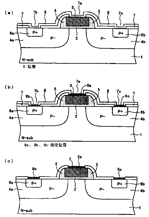
图1是说明本发明的第1实施例的半导体装置的制造方法的剖面图。FIG. 1 is a cross-sectional view illustrating a method of manufacturing a semiconductor device according to a first embodiment of the present invention.
图2是说明本发明的第1实施例的半导体装置的制造方法的剖面图。2 is a cross-sectional view illustrating a method of manufacturing the semiconductor device according to the first embodiment of the present invention.
图3是说明本发明的第1实施例的半导体装置的制造方法的剖面图。3 is a cross-sectional view illustrating a method of manufacturing the semiconductor device according to the first embodiment of the present invention.
图4是本发明的第1实施例的半导体装置的平面图。4 is a plan view of a semiconductor device according to a first embodiment of the present invention.
图5是说明本发明的第2实施例的半导体装置的制造方法的剖面图。5 is a cross-sectional view illustrating a method of manufacturing a semiconductor device according to a second embodiment of the present invention.
图6是现有例的半导体装置的剖面图。6 is a cross-sectional view of a conventional semiconductor device.
图7是显示例的其它半导体装置的剖面图。FIG. 7 is a cross-sectional view of another semiconductor device showing an example.
具体实施方式Detailed ways
下面参照附图,说明本发明的实施例的半导体装置及其制造方法。Hereinafter, a semiconductor device and a manufacturing method thereof according to an embodiment of the present invention will be described with reference to the drawings.
参照图1至图4,对第1实施例进行说明。图1至图3是表示该半导体装置的制造方法的剖面图,图4是该半导体装置的平面图。如图1(a)所示,在N型硅基板上形成例如由氧化硅膜构成的栅极绝缘膜2,在该栅极绝缘膜2上形成例如由多晶硅构成的栅电极3。A first embodiment will be described with reference to FIGS. 1 to 4 . 1 to 3 are cross-sectional views illustrating a method of manufacturing the semiconductor device, and FIG. 4 is a plan view of the semiconductor device. As shown in FIG. 1( a ), a gate
接着,如图1(b)所示,在邻接于栅电极3的N型硅基板1的表面上形成P-型扩散层4a、4b。具体是,以栅电极3为掩模,将硼等P型杂质以低浓度离子注入到N型硅基板1的表面,然后进行热扩散。P-型扩散层4a、4b的杂质浓度例如为1×10¹⁷/cm3左右,对此并未限定。Next, as shown in FIG. 1( b ), P − -
接下来,如图1(c)所示,在栅电极3的侧面上形成井壁衬垫绝缘膜5。该工序是通过首先利用CVD法在整个面上堆积氧化硅膜,然后各向异性蚀刻加工该氧化硅膜来进行的。在该蚀刻工序中,除去P-型扩散层4a、4b的表面的栅极绝缘膜2。Next, as shown in FIG. 1( c ), a well wall
接着,如图2(a)所示,将硼等P型杂质以高浓度离子注入到N型硅基板1的表面,形成P+型扩散层6a、6b。只离开栅电极3所定的距离地形成P+型扩散层6a、6b。由此,在井壁衬垫绝缘膜5和P+型扩散层6a、6b之间,P-型扩散层4a、4b露出到N型硅基板1的表面。而且,由P-型扩散层4a和P+型扩散层6a构成源极层,由P-型扩散层4b和P-型扩散层6b构成漏极层。Next, as shown in FIG. 2(a), P-type impurities such as boron are ion-implanted into the surface of the N-
接下来,如图2(b)所示,在整个面上堆积例如由氧化硅膜构成的硅化物阻挡层7,如图2(c)所示,通过有选择地对硅化物阻挡层7进行蚀刻,而在栅电极3上的硅化物阻挡层7上开设开口部7a,在P+型扩散层6a、6b上的硅化物阻挡层7上分别开设开口部7b、7c。Next, as shown in FIG. 2(b), a
然后,如图3(a)所示,通过在整个面上溅射钛(Ti)而形成钛层8。由此,栅电极3通过开口部7a而与钛层8接触,P+型扩散层6a、6b分别通过开口部7b、7c而与钛层8接触。Then, as shown in FIG. 3( a ),
其后,如图3(b)所示,通过进行热处理,从而接触栅电极3及P+型扩散层6a、6b的钛层8局部地硅化物化,分别在栅电极3上的表面形成硅化钛层9a,在P+型扩散层6a、6b的表面上形成硅化钛层9b、9c。Thereafter, as shown in FIG. 3( b ), by performing heat treatment, the
而且,如图3(c)所示,湿式蚀刻除去没有硅化物化的硅化物阻挡层7上的钛层8。再者,图3(c)对应于沿图4的平面图X-X线的剖面。Furthermore, as shown in FIG. 3(c), the
接着,参照图5说明本发明的第2实施例。对与图1至图4相同的构成部分赋予相同的符号,并省略说明。经过图1(a)、(b)、(c)、图2(a)的工序,在形成了P+型扩散层6a、6b的N型硅基板1的整个面上通过溅射钛而形成钛层10。Next, a second embodiment of the present invention will be described with reference to FIG. 5 . Components that are the same as those in FIGS. 1 to 4 are given the same reference numerals, and description thereof will be omitted. Through the steps of Fig. 1(a), (b), (c) and Fig. 2(a), titanium is formed by sputtering titanium on the entire surface of the N-
然后,如图5(b)所示,通过选择性地蚀刻钛层10,而在栅电极3的表面上残留钛层10a,分别在P+型扩散层6a、6b的表面上残留钛层10a、10b,除去除此之外的区域上的钛层10。此后,如图5(c)所示,通过进行热处理,而将钛层10a、10b、10c硅化物化,以形成硅化钛层11a、11b、11c。Then, as shown in FIG. 5( b), by selectively etching the
而且,在第1实施例中,作为硅化物阻挡层7,也可以使用氧化硅膜以外的材料,例如氮化硅膜。另外,在第1及第2实施例中,也可以用其它高融点金属代替钛。此外,在第1及第2实施例中,以P沟道型MOS晶体管为例进行说明,但本发明对N沟道型MOS晶体管也同样适用。再者,在第1及第2实施例中,源极层及漏极层均有P-型扩散层4a、4b,但也可以是只源极层和漏极层的任一方具有P-型扩散层的结构。Furthermore, in the first embodiment, a material other than a silicon oxide film, for example, a silicon nitride film, may be used as the
Claims (8)
Applications Claiming Priority (2)
| Application Number | Priority Date | Filing Date | Title |
|---|---|---|---|
| JP2003344170A JP2005109389A (en) | 2003-10-02 | 2003-10-02 | Semiconductor device and manufacturing method thereof |
| JP2003344170 | 2003-10-02 |
Publications (1)
| Publication Number | Publication Date |
|---|---|
| CN1604340A true CN1604340A (en) | 2005-04-06 |
Family
ID=34537894
Family Applications (1)
| Application Number | Title | Priority Date | Filing Date |
|---|---|---|---|
| CN200410079728.4A Pending CN1604340A (en) | 2003-10-02 | 2004-09-17 | Semiconductor device and method for manufacturing same |
Country Status (5)
| Country | Link |
|---|---|
| US (1) | US7468303B2 (en) |
| JP (1) | JP2005109389A (en) |
| KR (1) | KR100659619B1 (en) |
| CN (1) | CN1604340A (en) |
| TW (1) | TWI260783B (en) |
Cited By (5)
| Publication number | Priority date | Publication date | Assignee | Title |
|---|---|---|---|---|
| US7696050B2 (en) | 2005-10-04 | 2010-04-13 | Renesas Technology Corp. | Method of manufacturing semiconductor device carrying out ion implantation before silicide process |
| CN101814433B (en) * | 2009-02-20 | 2013-02-27 | 联发科技股份有限公司 | Lateral bipolar junction transistor and method of manufacturing the same |
| US8674454B2 (en) | 2009-02-20 | 2014-03-18 | Mediatek Inc. | Lateral bipolar junction transistor |
| CN103840001A (en) * | 2012-11-27 | 2014-06-04 | 台湾积体电路制造股份有限公司 | High voltage drain-extended mosfet having extra drain-od addition |
| CN112151610A (en) * | 2019-06-27 | 2020-12-29 | 南亚科技股份有限公司 | Semiconductor element and method for manufacturing the same |
Families Citing this family (9)
| Publication number | Priority date | Publication date | Assignee | Title |
|---|---|---|---|---|
| US7615426B2 (en) * | 2005-02-22 | 2009-11-10 | Taiwan Semiconductor Manufacturing Company, Ltd. | PMOS transistor with discontinuous CESL and method of fabrication |
| KR100928504B1 (en) * | 2007-10-19 | 2009-11-26 | 주식회사 동부하이텍 | Semiconductor Device and Manufacturing Method |
| KR100976793B1 (en) | 2007-12-31 | 2010-08-20 | 주식회사 동부하이텍 | Manufacturing method of MOS transistor |
| US20110065245A1 (en) * | 2009-09-13 | 2011-03-17 | Jei-Ming Chen | Method for fabricating mos transistor |
| JP2011222955A (en) * | 2010-03-26 | 2011-11-04 | Renesas Electronics Corp | Semiconductor device and method of manufacturing the same |
| CN102456556A (en) * | 2010-10-18 | 2012-05-16 | 中芯国际集成电路制造(上海)有限公司 | Formation method of metal silicide |
| US8569171B2 (en) * | 2011-07-01 | 2013-10-29 | Globalfoundries Inc. | Mask-based silicidation for FEOL defectivity reduction and yield boost |
| JP5927017B2 (en) * | 2012-04-20 | 2016-05-25 | ルネサスエレクトロニクス株式会社 | Semiconductor device and manufacturing method of semiconductor device |
| KR102288643B1 (en) * | 2019-03-29 | 2021-08-10 | 매그나칩 반도체 유한회사 | Mask layout, Semiconductor Device and Manufacturing Method using the same |
Family Cites Families (9)
| Publication number | Priority date | Publication date | Assignee | Title |
|---|---|---|---|---|
| US5208472A (en) * | 1988-05-13 | 1993-05-04 | Industrial Technology Research Institute | Double spacer salicide MOS device and method |
| US4949136A (en) * | 1988-06-09 | 1990-08-14 | University Of Connecticut | Submicron lightly doped field effect transistors |
| JP2551127B2 (en) * | 1989-01-07 | 1996-11-06 | 三菱電機株式会社 | MIS semiconductor device and manufacturing method thereof |
| WO1995019646A1 (en) * | 1994-01-12 | 1995-07-20 | Atmel Corporation | Input/output transistors with optimized esd protection |
| US6100125A (en) * | 1998-09-25 | 2000-08-08 | Fairchild Semiconductor Corp. | LDD structure for ESD protection and method of fabrication |
| JP3594550B2 (en) | 2000-11-27 | 2004-12-02 | シャープ株式会社 | Method for manufacturing semiconductor device |
| JP2002353330A (en) | 2001-05-25 | 2002-12-06 | Denso Corp | Semiconductor device and manufacturing method thereof |
| JP2003151991A (en) | 2001-08-23 | 2003-05-23 | Matsushita Electric Ind Co Ltd | Semiconductor device and manufacturing method thereof |
| KR20030058437A (en) | 2001-12-31 | 2003-07-07 | 동부전자 주식회사 | Method for manufacturing semiconductor device by using a groove |
-
2003
- 2003-10-02 JP JP2003344170A patent/JP2005109389A/en active Pending
-
2004
- 2004-09-17 CN CN200410079728.4A patent/CN1604340A/en active Pending
- 2004-10-01 KR KR1020040078182A patent/KR100659619B1/en not_active Expired - Fee Related
- 2004-10-01 TW TW093129796A patent/TWI260783B/en not_active IP Right Cessation
- 2004-10-01 US US10/954,370 patent/US7468303B2/en not_active Expired - Lifetime
Cited By (11)
| Publication number | Priority date | Publication date | Assignee | Title |
|---|---|---|---|---|
| US7696050B2 (en) | 2005-10-04 | 2010-04-13 | Renesas Technology Corp. | Method of manufacturing semiconductor device carrying out ion implantation before silicide process |
| CN1976007B (en) * | 2005-10-04 | 2010-06-16 | 株式会社瑞萨科技 | Semiconductor device and manufacturing method thereof |
| US7872314B2 (en) | 2005-10-04 | 2011-01-18 | Renesas Electronics Corporation | Method of manufacturing semiconductor device carrying out ion implantation before silicide process |
| CN101814433B (en) * | 2009-02-20 | 2013-02-27 | 联发科技股份有限公司 | Lateral bipolar junction transistor and method of manufacturing the same |
| US8674454B2 (en) | 2009-02-20 | 2014-03-18 | Mediatek Inc. | Lateral bipolar junction transistor |
| US8836043B2 (en) | 2009-02-20 | 2014-09-16 | Mediatek Inc. | Lateral bipolar junction transistor |
| US9324705B2 (en) | 2009-02-20 | 2016-04-26 | Mediatek Inc. | Lateral bipolar junction transistor |
| CN103840001A (en) * | 2012-11-27 | 2014-06-04 | 台湾积体电路制造股份有限公司 | High voltage drain-extended mosfet having extra drain-od addition |
| US9299806B2 (en) | 2012-11-27 | 2016-03-29 | Taiwan Semiconductor Manufacturing Company, Ltd. | High voltage drain-extended MOSFET having extra drain-OD addition |
| CN112151610A (en) * | 2019-06-27 | 2020-12-29 | 南亚科技股份有限公司 | Semiconductor element and method for manufacturing the same |
| CN112151610B (en) * | 2019-06-27 | 2024-04-16 | 南亚科技股份有限公司 | Semiconductor element and method for manufacturing the same |
Also Published As
| Publication number | Publication date |
|---|---|
| JP2005109389A (en) | 2005-04-21 |
| KR100659619B1 (en) | 2006-12-20 |
| TWI260783B (en) | 2006-08-21 |
| KR20050033018A (en) | 2005-04-08 |
| US20050104135A1 (en) | 2005-05-19 |
| TW200514259A (en) | 2005-04-16 |
| US7468303B2 (en) | 2008-12-23 |
Similar Documents
| Publication | Publication Date | Title |
|---|---|---|
| CN1604340A (en) | Semiconductor device and method for manufacturing same | |
| CN101069282A (en) | Method for forming self-aligned dual fully silicided gates in CMOS devies | |
| CN1624922A (en) | Complementary transistors with different source and drain extension spacing | |
| US8168488B2 (en) | Systems and methods for reducing contact to gate shorts | |
| CN113436969A (en) | Method for manufacturing semiconductor device | |
| CN1252834C (en) | MOSFET formed by using self-alignment silicide technology and its mfg. method | |
| US6774441B2 (en) | Semiconductor device having an MIS transistor | |
| CN1763970A (en) | Insulating spacers for thin insulating semiconductors | |
| CN1101059C (en) | Method for mfg. of semiconductor device | |
| CN1790672A (en) | CMOS image sensor and manufacturing method thereof | |
| CN1784774A (en) | CMOS integration for multi-thickness silicide devices | |
| CN1259729C (en) | Semiconductor device and manufacturing method thereof | |
| CN1722386A (en) | Metal oxide semiconductor transistor and its manufacturing method | |
| US6169025B1 (en) | Method of fabricating self-align-contact | |
| US20050212040A1 (en) | Semiconductor device having gate sidewall structure in silicide process and producing method of the semiconductor device | |
| CN101032017A (en) | Fabrication of Double Gate CMOS | |
| US20060163624A1 (en) | Semiconductor device, and manufacturing method thereof | |
| CN111415934B (en) | PMOS and NMOS integrated structure and manufacturing method thereof | |
| CN1638150A (en) | Semiconductor device and manufacturing method thereof | |
| US20050127446A1 (en) | Semiconductor device and method for manufacturing semiconductor device | |
| CN1868046A (en) | Semiconductor device and method of manufacturing such a semiconductor device | |
| EP1833087A1 (en) | Semiconductor device and method for manufacturing same | |
| US20080081444A1 (en) | Method for forming silicide layer on a silicon surface and its use | |
| JPH06326123A (en) | Method for manufacturing semiconductor device | |
| JPH0831949A (en) | Dual gate structure CMOS semiconductor device and manufacturing method thereof |
Legal Events
| Date | Code | Title | Description |
|---|---|---|---|
| C06 | Publication | ||
| PB01 | Publication | ||
| C10 | Entry into substantive examination | ||
| SE01 | Entry into force of request for substantive examination | ||
| C02 | Deemed withdrawal of patent application after publication (patent law 2001) | ||
| WD01 | Invention patent application deemed withdrawn after publication |