CN1909112B - Boosted circuit and semiconductor device with same - Google Patents
Boosted circuit and semiconductor device with same Download PDFInfo
- Publication number
- CN1909112B CN1909112B CN2006101086895A CN200610108689A CN1909112B CN 1909112 B CN1909112 B CN 1909112B CN 2006101086895 A CN2006101086895 A CN 2006101086895A CN 200610108689 A CN200610108689 A CN 200610108689A CN 1909112 B CN1909112 B CN 1909112B
- Authority
- CN
- China
- Prior art keywords
- circuit
- output
- signal
- control signal
- phase inverter
- Prior art date
- Legal status (The legal status is an assumption and is not a legal conclusion. Google has not performed a legal analysis and makes no representation as to the accuracy of the status listed.)
- Expired - Fee Related
Links
Images


Classifications
-
- G—PHYSICS
- G11—INFORMATION STORAGE
- G11C—STATIC STORES
- G11C16/00—Erasable programmable read-only memories
- G11C16/02—Erasable programmable read-only memories electrically programmable
- G11C16/06—Auxiliary circuits, e.g. for writing into memory
- G11C16/30—Power supply circuits
-
- G—PHYSICS
- G11—INFORMATION STORAGE
- G11C—STATIC STORES
- G11C16/00—Erasable programmable read-only memories
- G11C16/02—Erasable programmable read-only memories electrically programmable
- G11C16/06—Auxiliary circuits, e.g. for writing into memory
- G11C16/10—Programming or data input circuits
- G11C16/12—Programming voltage switching circuits
-
- G—PHYSICS
- G11—INFORMATION STORAGE
- G11C—STATIC STORES
- G11C5/00—Details of stores covered by group G11C11/00
- G11C5/14—Power supply arrangements, e.g. power down, chip selection or deselection, layout of wirings or power grids, or multiple supply levels
- G11C5/145—Applications of charge pumps; Boosted voltage circuits; Clamp circuits therefor
-
- H—ELECTRICITY
- H02—GENERATION; CONVERSION OR DISTRIBUTION OF ELECTRIC POWER
- H02M—APPARATUS FOR CONVERSION BETWEEN AC AND AC, BETWEEN AC AND DC, OR BETWEEN DC AND DC, AND FOR USE WITH MAINS OR SIMILAR POWER SUPPLY SYSTEMS; CONVERSION OF DC OR AC INPUT POWER INTO SURGE OUTPUT POWER; CONTROL OR REGULATION THEREOF
- H02M3/00—Conversion of DC power input into DC power output
- H02M3/02—Conversion of DC power input into DC power output without intermediate conversion into AC
- H02M3/04—Conversion of DC power input into DC power output without intermediate conversion into AC by static converters
- H02M3/06—Conversion of DC power input into DC power output without intermediate conversion into AC by static converters using resistors or capacitors, e.g. potential divider
- H02M3/07—Conversion of DC power input into DC power output without intermediate conversion into AC by static converters using resistors or capacitors, e.g. potential divider using capacitors charged and discharged alternately by semiconductor devices with control electrode, e.g. charge pumps
- H02M3/073—Charge pumps of the Schenkel-type
-
- H—ELECTRICITY
- H02—GENERATION; CONVERSION OR DISTRIBUTION OF ELECTRIC POWER
- H02M—APPARATUS FOR CONVERSION BETWEEN AC AND AC, BETWEEN AC AND DC, OR BETWEEN DC AND DC, AND FOR USE WITH MAINS OR SIMILAR POWER SUPPLY SYSTEMS; CONVERSION OF DC OR AC INPUT POWER INTO SURGE OUTPUT POWER; CONTROL OR REGULATION THEREOF
- H02M1/00—Details of apparatus for conversion
- H02M1/0003—Details of control, feedback or regulation circuits
- H02M1/0041—Control circuits in which a clock signal is selectively enabled or disabled
Landscapes
- Engineering & Computer Science (AREA)
- Power Engineering (AREA)
- Dc-Dc Converters (AREA)
- Semiconductor Integrated Circuits (AREA)
Abstract
一种能抑制升压电压的变异、抑制制造偏差的影响、避免电流峰值的增大的升压电路。它具备把检测升压电压而控制升压动作的判断输出信号(φ1)输出的电压检测电路(1)、振荡电路(2)和多个充电泵电路(3),振荡电路(2)具备奇数级控制型反相器(20),在来自电压检测电路(1)的判断输出信号(φ1)表示升压动作(有振荡)时,奇数级反相器构成开路,来自多个控制型反相器(20)的输出的振荡输出分别被取出,在判断输出信号(φ1)表示升压动作停止(振荡停止)时,不反相地保持控制型反相器(20)的输出值,停止振荡。多个充电泵电路(3)把来自控制型反相器(20)的输出信号(φ4~φ4″)作为时钟信号来接受而动作。
A booster circuit capable of suppressing the variation of the boosted voltage, suppressing the influence of the manufacturing deviation, and avoiding the increase of the current peak value. It has a voltage detection circuit (1), an oscillation circuit (2) and a plurality of charge pump circuits (3) that output a judgment output signal (φ1) that detects the boost voltage and controls the boost operation, and the oscillation circuit (2) has an odd number Stage-controlled inverters (20), when the judgment output signal (φ1) from the voltage detection circuit (1) indicates a step-up action (with oscillation), the odd-numbered-stage inverters constitute an open circuit, and multiple controlled inverters The oscillation output of the output of the inverter (20) is taken out respectively, and when the judgment output signal (φ1) indicates that the step-up operation stops (oscillation stop), the output value of the control type inverter (20) is kept without inversion, and the oscillation is stopped. . A plurality of charge pump circuits (3) operate by receiving output signals (φ4˜φ4″) from a control type inverter (20) as clock signals.
Description
技术领域 technical field
本发明涉及半导体装置,特别是涉及半导体存储器等的升压电压的生成所适用的升压电路,以及具备该升压电路的半导体装置。 The present invention relates to a semiconductor device, and in particular, to a booster circuit suitable for generating a boosted voltage of a semiconductor memory or the like, and a semiconductor device including the booster circuit. the
背景技术 Background technique
在以非易失性存储器为首的存储器电路中,为了进行存储单元的数据的改写和读取,需要产生高电压。 In a memory circuit including a nonvolatile memory, it is necessary to generate a high voltage in order to rewrite and read data in a memory cell. the
在用一般升压电路来产生高电压的场合,升压时的电流量超过电源的供给能力的话,就会导致电源电压的下降,因而就需要使峰值电流分散。 When a general booster circuit is used to generate a high voltage, if the amount of current during boosting exceeds the supply capacity of the power supply, the power supply voltage will drop, so it is necessary to disperse the peak current. the
作为其中之一,以前多用为了控制多个充电泵电路而使控制时钟信号的相位按每个充电泵来变化的方法。然而,需要对在产生相位差的过程中的延迟,以及在升压开始时和结束时多个控制时钟信号的同时变化下功夫。 As one of them, conventionally, a method of changing the phase of a control clock signal for each charge pump in order to control a plurality of charge pump circuits has been widely used. However, it is necessary to take care of the delay in generating the phase difference, and the simultaneous change of a plurality of control clock signals at the start and end of boosting. the
在专利文献1中,作为使由于单元数据放大时的噪声和升压电路动作所涉及的噪声的重复而产生的峰值电流进行分散,使单元数据放大得以稳定的升压电路,披露了图5所示的构成。参照图5,此升压电路具备:对升压电压进行检测,输出对升压动作进行控制的判断输出信号φ1的电压检测电路1;接受来自电压检测电路1的判断输出信号φ1的控制,输出振荡输出信号φ2的振荡电路21;接受电压检测电路1和振荡电路21各自的输出信号,控制充电泵电路的多个控制电路5;以及受控制电路5的控制而动作的多个充电泵电路3。控制电路5具备:输入振荡电路21的输出信号φ2,控制其反相信号及该输出信号φ2的 传递的传输门TG2、TG3;锁存传输门TG2、TG3的输出连接点的信号φ3,将其向充电泵电路输出,由判断输出信号φ1来控制激活化的第1锁存电路6;通过由判断输出信号φ1来控制导通的传输门TG4而对此信号φ3进行锁存的第2锁存电路7;控制传输门TG2、TG3,使得根据信号φ3及其反相信号φ3-(第2锁存电路7中的反相输出信号)和电压检测电路1的判断输出信号φ1,选择、输出振荡电路的输出信号φ2的逻辑的正相和反相中的与由第2锁存电路7锁存了的信号的逻辑反相的一方的电路8。
图8表示电压检测电路1的构成的一个例子。参照图8,电压检测电路1构成为,用电阻来分割升压节点VB的电位,用比较器COMP将其与基准电压VREF进行比较。如果VB的电位比由电阻分割比和基准电压VREF决定的设定电位低,作为比较器输出的判断输出信号φ1就变为高电平(有升压动作),反过来,如果VB的电位一方高,判断输出信号φ1就变为低电平(无升压动作)。
FIG. 8 shows an example of the configuration of the
还有,图9表示充电泵电路3的构成的一个例子。图9所示的构成称为互补型电路方式,由图5的φ3(或图1的φ4)的方波来控制。电容器C1及C2反相动作。
In addition, FIG. 9 shows an example of the configuration of the
图6是说明图5所示的构成的动作的定时波形图。如图6(a)所示,由电压检测电路1判定为升压电压达到了设定电压的话,判断输出信号φ1(φ1'、φ1″)就从高电平变为低电平,充电泵电路的控制信号φ3(φ3'、φ3″)由第1、第2锁存电路6、7保持,充电泵电路3停止,另一方面,振荡电路21的输出φ2(φ2'、φ2″)回到初期状态。
FIG. 6 is a timing waveform diagram illustrating the operation of the configuration shown in FIG. 5 . As shown in Figure 6(a), if the
由电压检测电路1判定为升压电压不到设定电压的话,判断输出信号φ1(φ1'、φ1″)就从低电平变为高电平,信号φ3(φ3'、φ3″),由于第2锁存电路7中保持的电平强制地切换振荡电路21的输出信号φ2的正、负逻辑,结果就使以第1锁存电路6中保持的电平的负 逻辑为起点的计时开始,使充电泵电路3中的动作再开始,进行升压动作。
If it is judged by the
专利文献1:特开平11-25673号公报 Patent Document 1: Japanese Patent Application Laid-Open No. 11-25673
发明内容 Contents of the invention
在参照图5及图6说明了的现有升压电路中,多个充电泵3由判断输出信号φ1和通过延迟元件而延迟,带有相位差的φ1'、…φ1″来控制,因而判断输出信号φ1从高电平变为低电平之后,到充电泵电路3的动作停止为止,会产生延迟。图6(a)的Td1(从φ1的变迁到φ1″的变迁为止的延迟时间)表示此延迟。
In the existing booster circuit described with reference to Fig. 5 and Fig. 6, a plurality of
在此场合,在图7中,如虚线所示,升压电压的变异变大,这是存在的课题。另外,图7是为了更易懂地说明参照图5及图6说明了的现有升压电路的课题而新作成的图,是表示了升压电压的时间推移的图,图7的虚线表示了图6(a)的Td1的延迟所涉及的影响。 In this case, in FIG. 7, as indicated by the dotted line, the variation of the boosted voltage becomes large, which is a problem. In addition, FIG. 7 is a diagram newly created to explain the problems of the conventional booster circuit described with reference to FIG. 5 and FIG. The influence of the delay involved in Td1 of Fig. 6(a). the
还有,判断输出信号φ1、φ1'、…φ1″的相位差根据延迟元件的延迟时间而产生,因而受制造偏差的影响,这是存在课题。 In addition, the phase difference of the judgment output signal φ1, φ1', ... φ1″ is generated according to the delay time of the delay element, so it is affected by the manufacturing variation, which is an existing problem.
再有,如图6(b)所示,相对于振荡电路21的周期,在从φ1到φ1″的延迟时间大的场合,在定时t1、t2、t3、…,φ3、φ3″的定时重叠,多个充电泵电路3会同时动作。因此,电流峰值会增加,这是存在课题。
Furthermore, as shown in FIG. 6(b), when the delay time from φ1 to φ1” is large with respect to the cycle of the
本申请所披露的发明,为了解决上述课题,大致构成如下。 In order to solve the above-mentioned problems, the invention disclosed in this application is roughly configured as follows. the
本发明的一个方面(侧面)所涉及的升压电路,具备:输入对振荡的有无进行控制的控制信号,在上述控制信号表示有振荡时,奇数级反相器构成闭合电路,来自多个上述反相器的输出端的振荡输出分别被 取出,在上述控制信号表示无振荡时,控制上述反相器的反相动作,使振荡停止的振荡电路;以及把来自上述振荡电路的多个振荡输出分别作为时钟来接受而动作的多个充电泵电路。 A booster circuit according to one aspect (side) of the present invention is provided with: inputting a control signal for controlling the presence or absence of oscillation; The oscillating output of the output terminal of the above-mentioned inverter is respectively taken out, and when the above-mentioned control signal indicates no oscillation, the inverting operation of the above-mentioned inverter is controlled to stop the oscillation; and a plurality of oscillation outputs from the above-mentioned oscillating circuit are output A plurality of charge pump circuits that each receive and operate as a clock. the
在本发明的升压电路中,上述振荡电路在上述控制信号表示无振荡时,不反相地保持上述反相器的输出值,停止振荡。 In the booster circuit according to the present invention, when the control signal indicates no oscillation, the oscillation circuit holds the output value of the inverter without inversion, and stops oscillation. the
在本发明的升压电路中,也可以构成为,上述振荡电路在上述控制信号表示无振荡的期间,把上述反相器的输出保持为在上述控制信号从有振荡向无振荡变迁了的时点的上述反相器的输出的值,停止振荡。 In the booster circuit of the present invention, the oscillating circuit may hold the output of the inverter at the time when the control signal transitions from oscillation to non-oscillation during a period in which the control signal indicates no oscillation. point above the value of the output of the inverter, the oscillation is stopped. the
在本发明的升压电路中,也可以构成为,上述振荡电路在上述控制信号表示无振荡的期间,把上述反相器的输入和输出的关系原样维持为在上述控制信号从有振荡向无振荡变迁了的时点的上述反相器的输入和输出的关系,停止振荡。 In the booster circuit of the present invention, the oscillating circuit may maintain the relationship between the input and output of the inverter as it is when the control signal changes from oscillating to non-oscillating during the period when the control signal indicates no oscillation. The relationship between the input and output of the above-mentioned inverter at the point in time when the oscillation has changed stops the oscillation. the
根据本发明,使得振荡电路的暂时停止和再开始的控制成为可能,能进行多个充电泵电路的同时停止和顺畅的动作开始。结果就能提高升压精度。 According to the present invention, it is possible to control the temporary stop and restart of the oscillation circuit, and it is possible to simultaneously stop and smoothly start operation of a plurality of charge pump circuits. As a result, boosting accuracy can be improved. the
还有,根据本发明,消除了多个充电泵控制信号的相位相重叠的可能性,抑制了制造偏差等所涉及的电流峰值的增加的产生。 Also, according to the present invention, the possibility of overlapping phases of a plurality of charge pump control signals is eliminated, and the occurrence of an increase in the current peak value due to manufacturing variation or the like is suppressed. the
附图说明 Description of drawings
图1是表示本发明的一实施例的构成的图。 FIG. 1 is a diagram showing the configuration of an embodiment of the present invention. the
图2(a)是表示控制型反相器的电路构成的图,(b)是表示动作的图。 Fig. 2(a) is a diagram showing a circuit configuration of a control type inverter, and Fig. 2(b) is a diagram showing its operation. the
图3是表示本发明的一实施例的升压电路的动作的定时图。 FIG. 3 is a timing chart showing the operation of the booster circuit according to one embodiment of the present invention. the
图4是表示控制型反相器的别的构成例的图。 FIG. 4 is a diagram showing another configuration example of a control-type inverter. the
图5是表示专利文献1的升压电路的构成的图。
FIG. 5 is a diagram showing the configuration of a booster circuit in
图6(a)、(b)是说明现有升压电路的动作的图。 6( a ), ( b ) are diagrams illustrating the operation of a conventional booster circuit. the
图7是表示升压电压的时间推移的图。 FIG. 7 is a graph showing time transition of a boosted voltage. the
图8是表示电压检测电路的构成的一个例子的图。 FIG. 8 is a diagram showing an example of a configuration of a voltage detection circuit. the
图9是表示充电泵电路的构成的一个例子的图。 FIG. 9 is a diagram showing an example of a configuration of a charge pump circuit. the
标号说明 Label description
1电压检测电路 1 voltage detection circuit
2振荡电路 2 oscillator circuit
3充电泵电路 3 charge pump circuit
5控制电路 5 control circuit
6锁存电路 6 latch circuit
7锁存电路 7 latch circuit
8F/F电路 8F/F circuit
20控制型反相器 20 control type inverter
21振荡电路 21 oscillator circuit
201 OR电路 201 OR circuit
202、203EXOR电路 202, 203 EXOR circuit
211、212、215、216反相器 211, 212, 215, 216 inverters
213 NMOS晶体管 213 NMOS transistors
214 PMOS晶体管 214 PMOS transistors
具体实施方式 Detailed ways
以下参照为进一步详细述说上述本发明的附图进行说明。本发明具备对升压电压进行检测的电压检测电路(1)、振荡电路(2)和多个充电泵电路(3),振荡电路(2)具备奇数级控制型反相器(20),在来自电压检测电路(1)的控制信号(φ1)表示有振荡(执行升压动作)时,奇数级反相器构成闭合电路,从多个控制型反相器(20)的输出中,振荡输出(φ4、φ4'、…φ4″)分别被取出,作为时钟信号被供给到多个充电泵电路(3)。另一方面,在控制信号(φ1)表示振荡停止(停止升压动作)时,控制型反相器(20)的输出值不反相地被保持,因此,振荡被停止。此时, 多个充电泵电路(3)中,来自振荡电路(2)的多个输出信号(φ4、φ4'、…φ4″)被保持为多个控制型反相器(20)的输出保持值而不振荡,多个充电泵电路(3)停止动作。在本发明中,在振荡电路的控制型反相器(20)的构成上有几种变形。以下就实施例进行说明。 The following description will be made with reference to the accompanying drawings for further detailing the above-mentioned present invention. The present invention includes a voltage detection circuit (1) for detecting a boosted voltage, an oscillation circuit (2) and a plurality of charge pump circuits (3), and the oscillation circuit (2) has an odd-numbered stage control type inverter (20), and When the control signal (φ1) from the voltage detection circuit (1) indicates that there is oscillation (boosting operation is performed), the odd-numbered inverters form a closed circuit, and from the output of multiple control-type inverters (20), the oscillation output (φ4, φ4', ... φ4″) are taken out respectively, and supplied as clock signals to a plurality of charge pump circuits (3). On the other hand, when the control signal (φ1) indicates that the oscillation is stopped (the step-up operation is stopped), The output value of the control type inverter (20) is held without inversion, therefore, the oscillation is stopped. At this time, in a plurality of charge pump circuits (3), a plurality of output signals (φ4 , φ4', ... φ4") are maintained as output holding values of multiple control-type inverters (20) without oscillation, and multiple charge pump circuits (3) stop operating. In the present invention, there are several modifications in the configuration of the control type inverter (20) of the oscillation circuit. Examples are described below. the
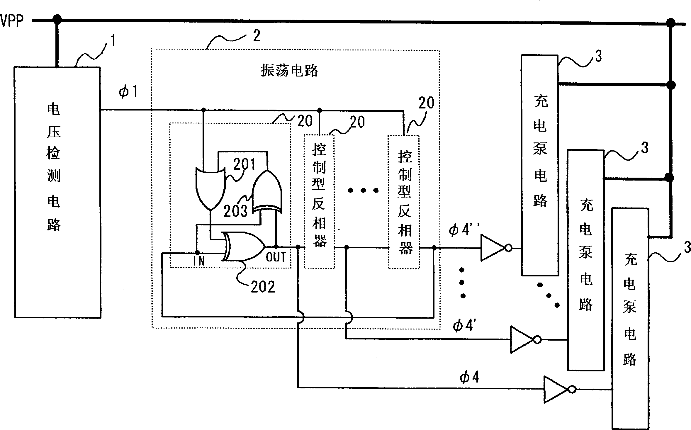
图1是表示本发明的一实施例的升压电路的构成的图。参照图1,本实施例的升压电路具备:输出对升压电压VPP进行检测,对升压动作进行控制的判断输出信号φ1的电压检测电路1;接受来自电压检测电路1的判断输出信号φ1,进行以判断输出信号φ1的值为基础的振荡动作·振荡停止的控制的振荡电路2;以及分别接受从振荡电路2输出的彼此相位不相同的输出信号φ4、φ4'、…φ4″而动作的多个充电泵电路3。另外,图1的电压检测电路1及充电泵电路3与图8及图9所示的电路构成相同,因而省略其说明。
FIG. 1 is a diagram showing the configuration of a booster circuit according to an embodiment of the present invention. With reference to Fig. 1, the boost circuit of the present embodiment has: the
振荡电路2构成为由在判断输出信号φ1表示振荡动作时,按奇数级级联方式连接控制型反相器20,把最末级的输出反馈输入到初级的闭合电路组成的环形振荡器。更详细的情况参照图1及图2,控制型反相器20具备从输入端输入判断输出信号φ1的或(OR)电路201、把向控制型反相器20的输入信号IN和OR电路201的输出信号作为输入的异或(EXOR)电路202以及把输入信号IN和异或(EXOR)电路202的输出信号OUT作为输入的异或(EXOR)电路203,在OR电路201的另一输入端,输入EXOR电路203的输出信号。对于控制型反相器20的动作进行说明。
在判断输出信号φ1为1(例如正逻辑下高电平)的场合,不论EXOR电路203的输出的值如何,OR电路201输出都为1,EXOR电路202作为反相器起作用而把输入信号IN的反相结果输出到输出OUT,作为反相电路起作用。
In the case of judging that the output signal φ1 is 1 (for example, a high level in positive logic), no matter what the value of the output of the
在判断输出信号φ1为0(例如正逻辑下低电平)的场合,OR电路 201的输出成为EXOR电路203的输出。在此场合,IN=1,OUT=0时(OUT=/IN;此处,/表示反相),EXOR电路203的输出变为1,OR电路201输出1,EXOR电路202的输出变为0,OUT变为IN的反相信号,OUT=/IN被维持。
When the judgment output signal φ1 is 0 (for example, low level in positive logic), the output of the
IN=0,OUT=1时(OUT=/IN),EXOR电路203的输出OUT变为1,OR电路201输出1,EXOR电路202的输出OUT变为1,OUT变为IN的反相信号,OUT=/IN被维持。
IN=0, when OUT=1 (OUT=/IN), the output OUT of
IN=1,OUT=1时(OUT=IN),EXOR电路203的输出变为0,OR电路201输出0,EXOR电路202的输出变为1,OUT=IN被维持。
When IN=1 and OUT=1 (OUT=IN), the output of the
IN=0,OUT=0时(OUT=IN),EXOR电路203的输出变为0,OR电路201输出0,EXOR电路202的输出变为0,OUT=IN被维持。
When IN=0 and OUT=0 (OUT=IN), the output of the
这样,在判断输出信号φ1为高电平的场合,OUT变为IN的反相信号(OUT=/IN),作为反相器而动作(参照图2(b))。 Thus, when the judgment output signal φ1 is at high level, OUT becomes an inverted signal of IN (OUT=/IN) and operates as an inverter (see FIG. 2(b)). the
另一方面,在判断输出信号φ1为低电平的场合,如果在判断输出信号φ1从高电平向低电平变迁时点OUT的反相完成了的话,OUT=/IN就被维持。还有,在判断输出信号φ1为低电平的场合,在判断输出信号φ1从高电平向低电平变迁时点,如果OUT的反相没完成(依赖于EXOR电路202的传播延迟时间等),OUT=IN就被维持。因此,不论反相器的动作状况如何,输出OUT都被保持。即,在判断输出信号φ1为低电平的期间,控制型反相器20的输出OUT的值被固定保持为判断输出信号φ1从高电平向低电平的变迁时点的值。
On the other hand, when the judgment output signal φ1 is at low level, if the inversion of OUT is completed when the judgment output signal φ1 transitions from high level to low level, OUT=/IN is maintained. In addition, when the judgment output signal φ1 is low level, if the inversion of OUT is not completed (depending on the propagation delay time of the
其次,对于图1的电路的控制动作进行说明。在由电压检测电路1判定为升压电压没达到设定电压的场合,判断输出信号φ1变为高电平,振荡电路2变为控制型反相器20的闭合电路,因而来自振荡电路 2的输出信号φ4、φ4'、…φ4″(来自环形振荡器的各级信号),根据各自的控制型反相器20的反相时间(从输入信号IN被输入到其反相信号OUT被输出的传播延迟时间),变为带有相位差的振荡信号。φ4和φ4'的相位差由构成环形振荡器的控制型反相器20的EXOR电路202的传播延迟时间来规定。
Next, the control operation of the circuit in FIG. 1 will be described. When it is judged by the
作为各自的时钟而接受来自振荡电路2的输出信号φ4、φ4'、…φ4″,多个充电泵电路3进行升压动作。
The output signals φ4, φ4', ... φ4" from the
另一方面,在由电压检测电路1判定为升压电压达到了设定电压的场合,判断输出信号φ1从高电平变为低电平,因此,振荡电路2内的全部的控制型反相器20的输出被保持。更详细的情况如上所述,在判断输出信号φ1为低电平的期间,控制型反相器20的输出被保持为判断输出信号φ1从高电平向低电平变迁了的时点的EXOR电路202的输出值。因此,在判断输出信号φ1为低电平时,来自振荡电路2的输出信号φ4、φ4'、…φ4″被分别持续维持为控制型反相器20的输出的保持值(高电平或低电平),振荡停止,多个充电泵电路3都不由时钟驱动,停止升压动作。
On the other hand, when it is judged by the
图3是用于说明本实施例的动作的定时图。如图3所示,判断输出信号φ1从高电平变为低电平的话,就振荡电路2的多个控制型反相器20的输出信号φ4、φ4'、…φ4″而言,其值全部被保持,由输出信号φ4、φ4'、…φ4″来控制动作的多个充电泵电路3停止升压动作。
FIG. 3 is a timing chart for explaining the operation of this embodiment. As shown in FIG. 3 , when the judgment output signal φ1 changes from a high level to a low level, the values of the output signals φ4, φ4′, ... φ4″ of the plurality of control-
判断输出信号φ1再次从低电平变为高电平的话,振荡电路2的控制型反相器20就作为反相器而动作。此时,例如输入输出电平以相等的状态(OUT=IN)被保持,来自多个控制型反相器20的输出信号φ4、φ4'、…φ4″的振荡再开始,作为时钟而接受输出信号φ4、φ4'、…φ4″的多个充电泵电路3分别进行升压动作。
When the judgment output signal φ1 changes from low level to high level again, the
根据上述控制动作,在本实施例中不必进行多余升压。 According to the control operation described above, it is not necessary to perform redundant voltage boosting in this embodiment. the
并且,在本实施例中,振荡电路2的输出φ4、φ4'、…φ4″间的相位差是分割了振荡电路2的振荡周期而成的(相当于EXOR电路202的传播延迟时间),因而多个振荡电路2φ4、φ4'、…φ4″的定时不会重叠。因此,在本实施例中,确实避免了多个充电泵电路3同时动作。结果,根据本实施例,抑制了峰值电流的增加的可能性。
And, in this embodiment, the phase difference among the outputs φ4, φ4', ... φ4" of the
对于本发明的别的实施例进行说明。在图1的振荡电路2中,控制型反相器20也可以是图4所示的构成。参照图4,此控制型反相器20是在反相器211的输出上配设了把来自电压检测电路1的判断输出信号φ1作为锁存控制信号来输入的锁存电路(由传输门和触发器组成)而成的。判断输出信号φ1为高电平时,锁存电路原样输出反相器211的输出(此处,输出被触发器保持),判断输出信号φ1为低电平时,锁存电路,因为传输门变为截止,所以不论输入信号IN的值如何,都输出被触发器保持的值。更详细的情况是具备对输入信号IN进行反相的反相器211、连接在输入信号IN和输出信号OUT之间的由PMOS晶体管214和NMOS晶体管213组成的传输门以及输入和输出互相连接的对输出信号OUT进行锁存的反相器215、216,NMOS晶体管213在栅极上接受电压检测电路1的判断输出信号φ1,PMOS晶体管214在栅极上接受由反相器212对判断输出信号φ1进行反相而成的信号。传输门(213、214)在判断输出信号φ1为高电平、低电平时,分别导通、截止。
Another embodiment of the present invention will be described. In the
在判断输出信号φ1为高电平的场合,传输门(213、214)导通,此时的输出被触发器电路(反相器215、216)保持。另一方面,在判断输出信号φ1为低电平的场合,传输门(213、214)变为非导通,触发器电路(215、216)所保持的电平被输出。此时反相器216把判断输出信号φ1将要变为低电平的之前的输入信号IN经反相器211反相,通过了传输 门(213、214)所得的信号电平向OUT输出(OUT=/IN)。 When the judgment output signal φ1 is at high level, the transmission gates (213, 214) are turned on, and the output at this time is held by flip-flop circuits (inverters 215, 216). On the other hand, when the judgment output signal φ1 is low level, the transfer gates (213, 214) are rendered non-conductive, and the level held by the flip-flop circuits (215, 216) is output. At this time, the inverter 216 inverts the input signal IN before the judgment output signal φ1 will become low level through the inverter 211, and the signal level obtained by the transmission gate (213, 214) is output to OUT (OUT =/IN). the
在把图4的控制型反相器20用于图1的振荡电路2的场合也是,与参照图3说明了的上述实施例同样地动作。即,在由电压检测电路1判断为升压电压没达到设定电压的场合,判断输出信号φ1变为高电平,振荡电路2变为奇数级控制型反相器20的闭合电路,振荡电路2的输出信号φ4、φ4'、…φ4″,根据控制型反相器20的反相时间,变为带有相位差的振荡信号。接受振荡电路2的输出信号φ4、φ4'、…φ4″,多个充电泵电路3分别动作,进行升压。在由电压检测电路1判断为升压电压达到了设定电压的场合,判断输出信号φ1变为低电平,从振荡电路2的控制型反相器20(参照图4)输出控制型反相器20内的锁存电路所保持的电平。因此,振荡电路2的输出信号φ4、φ4'、…φ4″的振荡停止,多个充电泵电路3所涉及的升压也停止。判断输出信号φ1从低电平变为高电平的话,振荡电路2的控制型反相器就作为反相器而动作,因而根据以输入输出电平相等的状态被保持的控制型反相器20,输出信号φ4、φ4'、…φ4″的振荡再开始,使充电泵电路3的升压动作再开始。
Also when the
在把上述本实施例的升压电路用于非易失性存储器等LSI的场合,通过振荡电路的控制型反相器的动作控制,使得振荡电路的暂时停止成为可能。还有,能获得可避免由于以峰值电流的分散为目的相位分割而产生的延迟的影响的升压控制。即,根据本实施例,相位分割时的相位差是分割振荡电路的振荡周期而成的,因而多个振荡电路输出的时钟定时不会重叠,对峰值电流的分散有贡献。 When the booster circuit of the present embodiment described above is used in an LSI such as a nonvolatile memory, it is possible to temporarily stop the oscillation circuit by controlling the operation of the control type inverter of the oscillation circuit. In addition, it is possible to obtain boost control that avoids the influence of delay due to phase division for the purpose of peak current dispersion. That is, according to the present embodiment, the phase difference at the time of phase division is obtained by dividing the oscillation period of the oscillation circuit, so the clock timings output by a plurality of oscillation circuits do not overlap and contribute to the dispersion of peak current. the
以上就上述实施例说明了本发明,不过,本发明不仅限于上述实施例的构成,当然还包括在本发明的范围内本领域技术人员能做的各种变形、修正。 The present invention has been described above with reference to the above-mentioned embodiments. However, the present invention is not limited to the configuration of the above-mentioned embodiments, and of course includes various modifications and corrections that can be made by those skilled in the art within the scope of the present invention. the
Claims (8)
Applications Claiming Priority (3)
| Application Number | Priority Date | Filing Date | Title |
|---|---|---|---|
| JP2005-225576 | 2005-08-03 | ||
| JP2005225576 | 2005-08-03 | ||
| JP2005225576A JP4716812B2 (en) | 2005-08-03 | 2005-08-03 | Semiconductor device |
Publications (2)
| Publication Number | Publication Date |
|---|---|
| CN1909112A CN1909112A (en) | 2007-02-07 |
| CN1909112B true CN1909112B (en) | 2012-01-18 |
Family
ID=37700173
Family Applications (1)
| Application Number | Title | Priority Date | Filing Date |
|---|---|---|---|
| CN2006101086895A Expired - Fee Related CN1909112B (en) | 2005-08-03 | 2006-08-03 | Boosted circuit and semiconductor device with same |
Country Status (3)
| Country | Link |
|---|---|
| US (1) | US7446594B2 (en) |
| JP (1) | JP4716812B2 (en) |
| CN (1) | CN1909112B (en) |
Families Citing this family (3)
| Publication number | Priority date | Publication date | Assignee | Title |
|---|---|---|---|---|
| KR100870428B1 (en) * | 2007-09-07 | 2008-11-26 | 주식회사 하이닉스반도체 | High Voltage Generation Circuit of Semiconductor Memory Device |
| US20130002343A1 (en) * | 2011-06-29 | 2013-01-03 | Synopsys Inc. | High voltage regulation in charge pumps |
| JPWO2013128806A1 (en) * | 2012-02-28 | 2015-07-30 | パナソニックIpマネジメント株式会社 | Booster circuit |
Citations (2)
| Publication number | Priority date | Publication date | Assignee | Title |
|---|---|---|---|---|
| JP2000236657A (en) * | 1999-02-15 | 2000-08-29 | Nec Kyushu Ltd | Booster circuit |
| CN1574088A (en) * | 2003-06-16 | 2005-02-02 | 海力士半导体有限公司 | Apparatus for generating driving voltage for sense amplifier in a memory device |
Family Cites Families (5)
| Publication number | Priority date | Publication date | Assignee | Title |
|---|---|---|---|---|
| JP2917914B2 (en) * | 1996-05-17 | 1999-07-12 | 日本電気株式会社 | Boost circuit |
| JP3090097B2 (en) * | 1997-06-30 | 2000-09-18 | 日本電気株式会社 | Boost circuit and control method thereof |
| US7135934B2 (en) * | 2005-03-01 | 2006-11-14 | Freescale, Semiconductor, Inc. | Fully programmable phase locked loop |
| KR100716661B1 (en) * | 2005-03-31 | 2007-05-09 | 주식회사 하이닉스반도체 | Voltage booster circuit |
| US7425874B2 (en) * | 2006-06-30 | 2008-09-16 | Texas Instruments Incorporated | All-digital phase-locked loop for a digital pulse-width modulator |
-
2005
- 2005-08-03 JP JP2005225576A patent/JP4716812B2/en not_active Expired - Fee Related
-
2006
- 2006-08-01 US US11/496,398 patent/US7446594B2/en not_active Expired - Fee Related
- 2006-08-03 CN CN2006101086895A patent/CN1909112B/en not_active Expired - Fee Related
Patent Citations (2)
| Publication number | Priority date | Publication date | Assignee | Title |
|---|---|---|---|---|
| JP2000236657A (en) * | 1999-02-15 | 2000-08-29 | Nec Kyushu Ltd | Booster circuit |
| CN1574088A (en) * | 2003-06-16 | 2005-02-02 | 海力士半导体有限公司 | Apparatus for generating driving voltage for sense amplifier in a memory device |
Also Published As
| Publication number | Publication date |
|---|---|
| US7446594B2 (en) | 2008-11-04 |
| US20070030082A1 (en) | 2007-02-08 |
| JP4716812B2 (en) | 2011-07-06 |
| JP2007043826A (en) | 2007-02-15 |
| CN1909112A (en) | 2007-02-07 |
Similar Documents
| Publication | Publication Date | Title |
|---|---|---|
| KR100347144B1 (en) | High voltage generating circuit | |
| TWI287794B (en) | Internal voltage generators for semiconductor memory devices | |
| JP2758881B2 (en) | Complementary clock generation method and complementary clock generator | |
| KR100399359B1 (en) | Charge pump circuit | |
| KR20120061564A (en) | Voltage supply circuit and method | |
| CN1909112B (en) | Boosted circuit and semiconductor device with same | |
| JPH09320267A (en) | Boosting circuit driving method and boosting circuit | |
| CN108092501B (en) | Booster circuit and nonvolatile memory including the booster circuit | |
| US20010048338A1 (en) | Boosting method and apparatus | |
| CN101120415B (en) | Synchronization type storage device and its control method | |
| JP2004147458A (en) | Boosting circuit | |
| CN116599465B (en) | Oscillator circuit and memory chip | |
| US6654306B2 (en) | Apparatus and method for generating an oscillating signal | |
| KR100282442B1 (en) | High voltage generator | |
| JP2016139921A (en) | Output circuit and integrated circuit | |
| KR100418719B1 (en) | Pumping circuit for flash memory device | |
| KR100908536B1 (en) | Current consumption prevention device of high voltage generator | |
| CN115248999B (en) | Method and apparatus for controlling clock signals | |
| JP6783879B2 (en) | Charge pump circuit | |
| CN118631218A (en) | Semiconductor devices | |
| TW202439765A (en) | A method for performing a charge-sharing operation and a charge pump circuit thereof | |
| CN115706519A (en) | Boost clock generator | |
| KR101174417B1 (en) | Multi level high voltage switch | |
| JP5292912B2 (en) | Pulse boosting circuit and pulse boosting method | |
| CN120544625A (en) | Low power charge pump system |
Legal Events
| Date | Code | Title | Description |
|---|---|---|---|
| C06 | Publication | ||
| PB01 | Publication | ||
| C10 | Entry into substantive examination | ||
| SE01 | Entry into force of request for substantive examination | ||
| C14 | Grant of patent or utility model | ||
| GR01 | Patent grant | ||
| C17 | Cessation of patent right | ||
| CF01 | Termination of patent right due to non-payment of annual fee |
Granted publication date: 20120118 Termination date: 20130803 |