CN1941299A - Semiconductor device and manufacturing method thereof - Google Patents
Semiconductor device and manufacturing method thereof Download PDFInfo
- Publication number
- CN1941299A CN1941299A CNA2006101413295A CN200610141329A CN1941299A CN 1941299 A CN1941299 A CN 1941299A CN A2006101413295 A CNA2006101413295 A CN A2006101413295A CN 200610141329 A CN200610141329 A CN 200610141329A CN 1941299 A CN1941299 A CN 1941299A
- Authority
- CN
- China
- Prior art keywords
- film
- semiconductor device
- oxide
- light
- manufacture method
- Prior art date
- Legal status (The legal status is an assumption and is not a legal conclusion. Google has not performed a legal analysis and makes no representation as to the accuracy of the status listed.)
- Granted
Links
Images




Classifications
-
- H—ELECTRICITY
- H10—SEMICONDUCTOR DEVICES; ELECTRIC SOLID-STATE DEVICES NOT OTHERWISE PROVIDED FOR
- H10D—INORGANIC ELECTRIC SEMICONDUCTOR DEVICES
- H10D30/00—Field-effect transistors [FET]
- H10D30/60—Insulated-gate field-effect transistors [IGFET]
- H10D30/67—Thin-film transistors [TFT]
- H10D30/6757—Thin-film transistors [TFT] characterised by the structure of the channel, e.g. transverse or longitudinal shape or doping profile
-
- G—PHYSICS
- G02—OPTICS
- G02F—OPTICAL DEVICES OR ARRANGEMENTS FOR THE CONTROL OF LIGHT BY MODIFICATION OF THE OPTICAL PROPERTIES OF THE MEDIA OF THE ELEMENTS INVOLVED THEREIN; NON-LINEAR OPTICS; FREQUENCY-CHANGING OF LIGHT; OPTICAL LOGIC ELEMENTS; OPTICAL ANALOGUE/DIGITAL CONVERTERS
- G02F1/00—Devices or arrangements for the control of the intensity, colour, phase, polarisation or direction of light arriving from an independent light source, e.g. switching, gating or modulating; Non-linear optics
- G02F1/01—Devices or arrangements for the control of the intensity, colour, phase, polarisation or direction of light arriving from an independent light source, e.g. switching, gating or modulating; Non-linear optics for the control of the intensity, phase, polarisation or colour
- G02F1/165—Devices or arrangements for the control of the intensity, colour, phase, polarisation or direction of light arriving from an independent light source, e.g. switching, gating or modulating; Non-linear optics for the control of the intensity, phase, polarisation or colour based on translational movement of particles in a fluid under the influence of an applied field
- G02F1/166—Devices or arrangements for the control of the intensity, colour, phase, polarisation or direction of light arriving from an independent light source, e.g. switching, gating or modulating; Non-linear optics for the control of the intensity, phase, polarisation or colour based on translational movement of particles in a fluid under the influence of an applied field characterised by the electro-optical or magneto-optical effect
- G02F1/167—Devices or arrangements for the control of the intensity, colour, phase, polarisation or direction of light arriving from an independent light source, e.g. switching, gating or modulating; Non-linear optics for the control of the intensity, phase, polarisation or colour based on translational movement of particles in a fluid under the influence of an applied field characterised by the electro-optical or magneto-optical effect by electrophoresis
-
- H—ELECTRICITY
- H10—SEMICONDUCTOR DEVICES; ELECTRIC SOLID-STATE DEVICES NOT OTHERWISE PROVIDED FOR
- H10D—INORGANIC ELECTRIC SEMICONDUCTOR DEVICES
- H10D30/00—Field-effect transistors [FET]
- H10D30/01—Manufacture or treatment
- H10D30/021—Manufacture or treatment of FETs having insulated gates [IGFET]
- H10D30/031—Manufacture or treatment of FETs having insulated gates [IGFET] of thin-film transistors [TFT]
-
- H—ELECTRICITY
- H10—SEMICONDUCTOR DEVICES; ELECTRIC SOLID-STATE DEVICES NOT OTHERWISE PROVIDED FOR
- H10D—INORGANIC ELECTRIC SEMICONDUCTOR DEVICES
- H10D30/00—Field-effect transistors [FET]
- H10D30/60—Insulated-gate field-effect transistors [IGFET]
- H10D30/67—Thin-film transistors [TFT]
-
- H—ELECTRICITY
- H10—SEMICONDUCTOR DEVICES; ELECTRIC SOLID-STATE DEVICES NOT OTHERWISE PROVIDED FOR
- H10D—INORGANIC ELECTRIC SEMICONDUCTOR DEVICES
- H10D30/00—Field-effect transistors [FET]
- H10D30/60—Insulated-gate field-effect transistors [IGFET]
- H10D30/67—Thin-film transistors [TFT]
- H10D30/674—Thin-film transistors [TFT] characterised by the active materials
- H10D30/6755—Oxide semiconductors, e.g. zinc oxide, copper aluminium oxide or cadmium stannate
-
- H—ELECTRICITY
- H10—SEMICONDUCTOR DEVICES; ELECTRIC SOLID-STATE DEVICES NOT OTHERWISE PROVIDED FOR
- H10D—INORGANIC ELECTRIC SEMICONDUCTOR DEVICES
- H10D30/00—Field-effect transistors [FET]
- H10D30/60—Insulated-gate field-effect transistors [IGFET]
- H10D30/67—Thin-film transistors [TFT]
- H10D30/674—Thin-film transistors [TFT] characterised by the active materials
- H10D30/6755—Oxide semiconductors, e.g. zinc oxide, copper aluminium oxide or cadmium stannate
- H10D30/6756—Amorphous oxide semiconductors
-
- H—ELECTRICITY
- H10—SEMICONDUCTOR DEVICES; ELECTRIC SOLID-STATE DEVICES NOT OTHERWISE PROVIDED FOR
- H10D—INORGANIC ELECTRIC SEMICONDUCTOR DEVICES
- H10D62/00—Semiconductor bodies, or regions thereof, of devices having potential barriers
- H10D62/40—Crystalline structures
-
- H—ELECTRICITY
- H10—SEMICONDUCTOR DEVICES; ELECTRIC SOLID-STATE DEVICES NOT OTHERWISE PROVIDED FOR
- H10D—INORGANIC ELECTRIC SEMICONDUCTOR DEVICES
- H10D62/00—Semiconductor bodies, or regions thereof, of devices having potential barriers
- H10D62/40—Crystalline structures
- H10D62/405—Orientations of crystalline planes
-
- H—ELECTRICITY
- H10—SEMICONDUCTOR DEVICES; ELECTRIC SOLID-STATE DEVICES NOT OTHERWISE PROVIDED FOR
- H10D—INORGANIC ELECTRIC SEMICONDUCTOR DEVICES
- H10D86/00—Integrated devices formed in or on insulating or conducting substrates, e.g. formed in silicon-on-insulator [SOI] substrates or on stainless steel or glass substrates
- H10D86/01—Manufacture or treatment
- H10D86/021—Manufacture or treatment of multiple TFTs
- H10D86/0221—Manufacture or treatment of multiple TFTs comprising manufacture, treatment or patterning of TFT semiconductor bodies
- H10D86/0223—Manufacture or treatment of multiple TFTs comprising manufacture, treatment or patterning of TFT semiconductor bodies comprising crystallisation of amorphous, microcrystalline or polycrystalline semiconductor materials
- H10D86/0229—Manufacture or treatment of multiple TFTs comprising manufacture, treatment or patterning of TFT semiconductor bodies comprising crystallisation of amorphous, microcrystalline or polycrystalline semiconductor materials characterised by control of the annealing or irradiation parameters
-
- H—ELECTRICITY
- H10—SEMICONDUCTOR DEVICES; ELECTRIC SOLID-STATE DEVICES NOT OTHERWISE PROVIDED FOR
- H10D—INORGANIC ELECTRIC SEMICONDUCTOR DEVICES
- H10D86/00—Integrated devices formed in or on insulating or conducting substrates, e.g. formed in silicon-on-insulator [SOI] substrates or on stainless steel or glass substrates
- H10D86/40—Integrated devices formed in or on insulating or conducting substrates, e.g. formed in silicon-on-insulator [SOI] substrates or on stainless steel or glass substrates characterised by multiple TFTs
- H10D86/421—Integrated devices formed in or on insulating or conducting substrates, e.g. formed in silicon-on-insulator [SOI] substrates or on stainless steel or glass substrates characterised by multiple TFTs having a particular composition, shape or crystalline structure of the active layer
- H10D86/423—Integrated devices formed in or on insulating or conducting substrates, e.g. formed in silicon-on-insulator [SOI] substrates or on stainless steel or glass substrates characterised by multiple TFTs having a particular composition, shape or crystalline structure of the active layer comprising semiconductor materials not belonging to the Group IV, e.g. InGaZnO
-
- H—ELECTRICITY
- H10—SEMICONDUCTOR DEVICES; ELECTRIC SOLID-STATE DEVICES NOT OTHERWISE PROVIDED FOR
- H10D—INORGANIC ELECTRIC SEMICONDUCTOR DEVICES
- H10D86/00—Integrated devices formed in or on insulating or conducting substrates, e.g. formed in silicon-on-insulator [SOI] substrates or on stainless steel or glass substrates
- H10D86/40—Integrated devices formed in or on insulating or conducting substrates, e.g. formed in silicon-on-insulator [SOI] substrates or on stainless steel or glass substrates characterised by multiple TFTs
- H10D86/60—Integrated devices formed in or on insulating or conducting substrates, e.g. formed in silicon-on-insulator [SOI] substrates or on stainless steel or glass substrates characterised by multiple TFTs wherein the TFTs are in active matrices
-
- H—ELECTRICITY
- H10—SEMICONDUCTOR DEVICES; ELECTRIC SOLID-STATE DEVICES NOT OTHERWISE PROVIDED FOR
- H10D—INORGANIC ELECTRIC SEMICONDUCTOR DEVICES
- H10D99/00—Subject matter not provided for in other groups of this subclass
-
- H—ELECTRICITY
- H10—SEMICONDUCTOR DEVICES; ELECTRIC SOLID-STATE DEVICES NOT OTHERWISE PROVIDED FOR
- H10P—GENERIC PROCESSES OR APPARATUS FOR THE MANUFACTURE OR TREATMENT OF DEVICES COVERED BY CLASS H10
- H10P14/00—Formation of materials, e.g. in the shape of layers or pillars
- H10P14/20—Formation of materials, e.g. in the shape of layers or pillars of semiconductor materials
- H10P14/22—Formation of materials, e.g. in the shape of layers or pillars of semiconductor materials using physical deposition, e.g. vacuum deposition or sputtering
-
- H—ELECTRICITY
- H10—SEMICONDUCTOR DEVICES; ELECTRIC SOLID-STATE DEVICES NOT OTHERWISE PROVIDED FOR
- H10P—GENERIC PROCESSES OR APPARATUS FOR THE MANUFACTURE OR TREATMENT OF DEVICES COVERED BY CLASS H10
- H10P14/00—Formation of materials, e.g. in the shape of layers or pillars
- H10P14/60—Formation of materials, e.g. in the shape of layers or pillars of insulating materials
- H10P14/63—Formation of materials, e.g. in the shape of layers or pillars of insulating materials characterised by the formation processes
- H10P14/6326—Deposition processes
- H10P14/6328—Deposition from the gas or vapour phase
- H10P14/6329—Deposition from the gas or vapour phase using physical ablation of a target, e.g. physical vapour deposition or pulsed laser deposition
-
- H—ELECTRICITY
- H10—SEMICONDUCTOR DEVICES; ELECTRIC SOLID-STATE DEVICES NOT OTHERWISE PROVIDED FOR
- H10P—GENERIC PROCESSES OR APPARATUS FOR THE MANUFACTURE OR TREATMENT OF DEVICES COVERED BY CLASS H10
- H10P14/00—Formation of materials, e.g. in the shape of layers or pillars
- H10P14/60—Formation of materials, e.g. in the shape of layers or pillars of insulating materials
- H10P14/69—Inorganic materials
- H10P14/692—Inorganic materials composed of oxides, glassy oxides or oxide-based glasses
- H10P14/6921—Inorganic materials composed of oxides, glassy oxides or oxide-based glasses containing silicon
- H10P14/69215—Inorganic materials composed of oxides, glassy oxides or oxide-based glasses containing silicon the material being a silicon oxide, e.g. SiO2
-
- H—ELECTRICITY
- H10—SEMICONDUCTOR DEVICES; ELECTRIC SOLID-STATE DEVICES NOT OTHERWISE PROVIDED FOR
- H10P—GENERIC PROCESSES OR APPARATUS FOR THE MANUFACTURE OR TREATMENT OF DEVICES COVERED BY CLASS H10
- H10P14/00—Formation of materials, e.g. in the shape of layers or pillars
- H10P14/60—Formation of materials, e.g. in the shape of layers or pillars of insulating materials
- H10P14/69—Inorganic materials
- H10P14/692—Inorganic materials composed of oxides, glassy oxides or oxide-based glasses
- H10P14/6938—Inorganic materials composed of oxides, glassy oxides or oxide-based glasses the material containing at least one metal element, e.g. metal oxides, metal oxynitrides or metal oxycarbides
- H10P14/6939—Inorganic materials composed of oxides, glassy oxides or oxide-based glasses the material containing at least one metal element, e.g. metal oxides, metal oxynitrides or metal oxycarbides characterised by the metal
- H10P14/69391—Inorganic materials composed of oxides, glassy oxides or oxide-based glasses the material containing at least one metal element, e.g. metal oxides, metal oxynitrides or metal oxycarbides characterised by the metal the material containing aluminium, e.g. Al2O3
-
- H—ELECTRICITY
- H10—SEMICONDUCTOR DEVICES; ELECTRIC SOLID-STATE DEVICES NOT OTHERWISE PROVIDED FOR
- H10P—GENERIC PROCESSES OR APPARATUS FOR THE MANUFACTURE OR TREATMENT OF DEVICES COVERED BY CLASS H10
- H10P14/00—Formation of materials, e.g. in the shape of layers or pillars
- H10P14/60—Formation of materials, e.g. in the shape of layers or pillars of insulating materials
- H10P14/69—Inorganic materials
- H10P14/694—Inorganic materials composed of nitrides
- H10P14/6943—Inorganic materials composed of nitrides containing silicon
- H10P14/69433—Inorganic materials composed of nitrides containing silicon the material being a silicon nitride not containing oxygen, e.g. SixNy or SixByNz
-
- H—ELECTRICITY
- H10—SEMICONDUCTOR DEVICES; ELECTRIC SOLID-STATE DEVICES NOT OTHERWISE PROVIDED FOR
- H10P—GENERIC PROCESSES OR APPARATUS FOR THE MANUFACTURE OR TREATMENT OF DEVICES COVERED BY CLASS H10
- H10P34/00—Irradiation with electromagnetic or particle radiation of wafers, substrates or parts of devices
- H10P34/40—Irradiation with electromagnetic or particle radiation of wafers, substrates or parts of devices with high-energy radiation
- H10P34/42—Irradiation with electromagnetic or particle radiation of wafers, substrates or parts of devices with high-energy radiation with electromagnetic radiation, e.g. laser annealing
-
- H—ELECTRICITY
- H10—SEMICONDUCTOR DEVICES; ELECTRIC SOLID-STATE DEVICES NOT OTHERWISE PROVIDED FOR
- H10P—GENERIC PROCESSES OR APPARATUS FOR THE MANUFACTURE OR TREATMENT OF DEVICES COVERED BY CLASS H10
- H10P50/00—Etching of wafers, substrates or parts of devices
- H10P50/20—Dry etching; Plasma etching; Reactive-ion etching
-
- H—ELECTRICITY
- H10—SEMICONDUCTOR DEVICES; ELECTRIC SOLID-STATE DEVICES NOT OTHERWISE PROVIDED FOR
- H10P—GENERIC PROCESSES OR APPARATUS FOR THE MANUFACTURE OR TREATMENT OF DEVICES COVERED BY CLASS H10
- H10P52/00—Grinding, lapping or polishing of wafers, substrates or parts of devices
-
- H—ELECTRICITY
- H10—SEMICONDUCTOR DEVICES; ELECTRIC SOLID-STATE DEVICES NOT OTHERWISE PROVIDED FOR
- H10P—GENERIC PROCESSES OR APPARATUS FOR THE MANUFACTURE OR TREATMENT OF DEVICES COVERED BY CLASS H10
- H10P95/00—Generic processes or apparatus for manufacture or treatments not covered by the other groups of this subclass
- H10P95/70—Chemical treatments
-
- H—ELECTRICITY
- H10—SEMICONDUCTOR DEVICES; ELECTRIC SOLID-STATE DEVICES NOT OTHERWISE PROVIDED FOR
- H10P—GENERIC PROCESSES OR APPARATUS FOR THE MANUFACTURE OR TREATMENT OF DEVICES COVERED BY CLASS H10
- H10P95/00—Generic processes or apparatus for manufacture or treatments not covered by the other groups of this subclass
- H10P95/90—Thermal treatments, e.g. annealing or sintering
-
- H—ELECTRICITY
- H10—SEMICONDUCTOR DEVICES; ELECTRIC SOLID-STATE DEVICES NOT OTHERWISE PROVIDED FOR
- H10P—GENERIC PROCESSES OR APPARATUS FOR THE MANUFACTURE OR TREATMENT OF DEVICES COVERED BY CLASS H10
- H10P14/00—Formation of materials, e.g. in the shape of layers or pillars
- H10P14/20—Formation of materials, e.g. in the shape of layers or pillars of semiconductor materials
- H10P14/34—Deposited materials, e.g. layers
- H10P14/3402—Deposited materials, e.g. layers characterised by the chemical composition
- H10P14/3424—Deposited materials, e.g. layers characterised by the chemical composition being Group IIB-VIA materials
- H10P14/3426—Oxides
-
- H—ELECTRICITY
- H10—SEMICONDUCTOR DEVICES; ELECTRIC SOLID-STATE DEVICES NOT OTHERWISE PROVIDED FOR
- H10P—GENERIC PROCESSES OR APPARATUS FOR THE MANUFACTURE OR TREATMENT OF DEVICES COVERED BY CLASS H10
- H10P14/00—Formation of materials, e.g. in the shape of layers or pillars
- H10P14/20—Formation of materials, e.g. in the shape of layers or pillars of semiconductor materials
- H10P14/34—Deposited materials, e.g. layers
- H10P14/3402—Deposited materials, e.g. layers characterised by the chemical composition
- H10P14/3434—Deposited materials, e.g. layers characterised by the chemical composition being oxide semiconductor materials
-
- H—ELECTRICITY
- H10—SEMICONDUCTOR DEVICES; ELECTRIC SOLID-STATE DEVICES NOT OTHERWISE PROVIDED FOR
- H10P—GENERIC PROCESSES OR APPARATUS FOR THE MANUFACTURE OR TREATMENT OF DEVICES COVERED BY CLASS H10
- H10P14/00—Formation of materials, e.g. in the shape of layers or pillars
- H10P14/20—Formation of materials, e.g. in the shape of layers or pillars of semiconductor materials
- H10P14/38—Formation of materials, e.g. in the shape of layers or pillars of semiconductor materials characterised by treatments done after the formation of the materials
- H10P14/3802—Crystallisation or recrystallisation of non-monocrystalline semiconductor materials, e.g. regrowth
Landscapes
- Physics & Mathematics (AREA)
- Nonlinear Science (AREA)
- Optics & Photonics (AREA)
- Chemical & Material Sciences (AREA)
- Life Sciences & Earth Sciences (AREA)
- Chemical Kinetics & Catalysis (AREA)
- Electrochemistry (AREA)
- Molecular Biology (AREA)
- General Physics & Mathematics (AREA)
- Health & Medical Sciences (AREA)
- Thin Film Transistor (AREA)
- Liquid Crystal (AREA)
- Electroluminescent Light Sources (AREA)
- Recrystallisation Techniques (AREA)
- Electrodes Of Semiconductors (AREA)
- Devices For Indicating Variable Information By Combining Individual Elements (AREA)
- Electrochromic Elements, Electrophoresis, Or Variable Reflection Or Absorption Elements (AREA)
- Electromagnetism (AREA)
- Crystallography & Structural Chemistry (AREA)
- Dram (AREA)
- Physical Vapour Deposition (AREA)
- Formation Of Insulating Films (AREA)
Abstract
Description
技术领域technical field
本发明涉及一种半导体器件及其制造方法。本发明特别涉及使用氧化物半导体的半导体器件。此外,本发明还涉及具备该半导体器件的电子设备。The invention relates to a semiconductor device and a manufacturing method thereof. In particular, the present invention relates to a semiconductor device using an oxide semiconductor. Furthermore, the present invention relates to electronic equipment including the semiconductor device.
背景技术Background technique
以液晶显示器(LCD)和EL显示器为典型的平板显示器(FPD)作为代替常规的CRT的显示器件引人注目。尤其是,安装有有源矩阵驱动的大型液晶面板的大屏幕液晶电视的开发对液晶面板的制造者已经成为该致力进行的重要课题。此外,大屏幕的EL电视的开发也在展开。A flat panel display (FPD) typified by a liquid crystal display (LCD) and an EL display is attracting attention as a display device replacing a conventional CRT. In particular, the development of a large-screen liquid crystal television equipped with a large liquid crystal panel driven by an active matrix has become an important task for liquid crystal panel manufacturers. In addition, the development of large-screen EL TV is also underway.
在常规的液晶器件或场致发光显示器件(以下称作发光显示器件或EL显示器件)中,使用结晶硅或非晶硅的薄膜晶体管(以下示为TFT)作为驱动每个像素的半导体元件。In a conventional liquid crystal device or electroluminescent display device (hereinafter referred to as light emitting display device or EL display device), a thin film transistor (hereinafter referred to as TFT) of crystalline silicon or amorphous silicon is used as a semiconductor element driving each pixel.
与使用非晶硅膜的TFT相比使用结晶硅膜的TFT的迁移率高二位以上(包括二位),从而当用于扫描线驱动电路或信号线驱动电路等时可以期待高速动作,所述扫描线驱动电路用于选择发光显示器件的像素,所述信号线驱动电路用于将视频信号供给给被选择了的像素。然而,与将非晶硅用作半导体膜时相比,将结晶硅用作半导体膜时为了使半导体膜结晶化而使步骤复杂化,从而具有一个难点,即成品率降低而且成本上升。此外,用于该结晶化的加热温度为550℃或更高,不易使用熔点低的树脂或塑料等的衬底。Compared with TFTs using amorphous silicon films, the mobility of TFTs using crystalline silicon films is higher by two digits or more (including two digits), so that high-speed operation can be expected when used in scanning line driving circuits or signal line driving circuits. The scanning line driving circuit is used to select pixels of the light-emitting display device, and the signal line driving circuit is used to supply video signals to the selected pixels. However, compared with the use of amorphous silicon as the semiconductor film, the use of crystalline silicon as the semiconductor film complicates the steps for crystallizing the semiconductor film, resulting in difficulties in that the yield decreases and the cost increases. In addition, the heating temperature for this crystallization is 550° C. or higher, and it is difficult to use a substrate such as resin or plastic with a low melting point.
另一方面,将非晶硅用作半导体膜的TFT由于不进行高温加热,所以可以使用树脂衬底或塑料衬底,从而可以以低成本制造。然而,使用非晶硅的半导体膜形成沟道形成区域的TFT的迁移率最大也只能得到0.2至1.0cm2/V·s左右,而且耗电量也高。On the other hand, since a TFT using amorphous silicon as a semiconductor film does not undergo high-temperature heating, a resin substrate or a plastic substrate can be used, and thus can be manufactured at low cost. However, a TFT in which a channel formation region is formed using an amorphous silicon semiconductor film has a mobility of only about 0.2 to 1.0 cm 2 /V·s at the maximum, and also has high power consumption.
此外,当将非晶硅膜形成在衬底上时,一般使用等离子体CVD法。等离子体CVD法当淀积时需要在高真空下进行的加热,有可能给在塑料衬底或衬底上的有机树脂膜损伤。此外,除了使用等离子体CVD法淀积非晶硅膜之外使用溅射法淀积时,也在非晶硅膜淀积了之后被暴露在空气中,则有可能在表面上形成很薄的绝缘膜。In addition, when forming an amorphous silicon film on a substrate, a plasma CVD method is generally used. The plasma CVD method requires heating under high vacuum when depositing, which may damage the plastic substrate or the organic resin film on the substrate. In addition, when the amorphous silicon film is deposited by the sputtering method other than the plasma CVD method, the amorphous silicon film is also exposed to the air after deposition, and it is possible to form a thin film on the surface. insulating film.
作为代替这种由硅构成的半导体的材料,近年来,有将氧化锌等氧化物半导体用于沟道形成区域来形成TFT的报告(例如参见专利文献1、非专利文献1)。由于氧化物半导体具有与由包括非晶硅的半导体构成的TFT相同或比它高的迁移率,所以被谋求进一步提高其特性。As a material replacing such a semiconductor made of silicon, in recent years, it has been reported that an oxide semiconductor such as zinc oxide is used in a channel formation region to form a TFT (for example, see Patent Document 1 and Non-Patent Document 1). Since an oxide semiconductor has mobility equal to or higher than that of a TFT composed of a semiconductor including amorphous silicon, it is sought to further improve its characteristics.
[专利文献1]日本专利申请特开2000-150900号[Patent Document 1] Japanese Patent Application Laid-Open No. 2000-150900
[非专利文献1]Elvira M.C.Fortunato以及六名Applied PhysicsLetters(应用物理快报)Vol.85、No.13、P 2541(2004)[Non-Patent Document 1] Elvira M.C.Fortunato and six Applied Physics Letters (Applied Physics Letters) Vol.85, No.13, P 2541 (2004)
发明内容Contents of the invention
鉴于上述课题,本发明的目的在于提供一种半导体器件和其制造方法,该半导体器件具有提高了特性的半导体元件。In view of the above problems, an object of the present invention is to provide a semiconductor device having a semiconductor element with improved characteristics and a method of manufacturing the same.
此外,另一方面,为了如液晶电视那样以更廉价的工序制造大面积装置,衬底的面积越来越大。然而,有一个问题,即因为衬底的大型化,容易受弯曲和扭曲的影响。此外,在热处理步骤中衬底被加热到高温度,就有一个问题,即扭曲和收缩导致衬底的尺寸的变化,从而光刻步骤的对准的精度降低。In addition, on the other hand, in order to manufacture a large-area device with a cheaper process such as a liquid crystal television, the area of the substrate is increasing. However, there is a problem in that it is easily affected by bending and twisting due to the upsizing of the substrate. In addition, the substrate is heated to a high temperature in the heat treatment step, and there is a problem that distortion and shrinkage cause a dimensional change of the substrate, thereby lowering the accuracy of alignment in the photolithography step.
由此,本发明的目的在于提供一种技术,该技术在用于半导体器件的半导体元件的结晶化步骤中即使在单边超过1米那样的大型衬底上也可以以高成品率制造半导体器件。Therefore, an object of the present invention is to provide a technique that can manufacture semiconductor devices with a high yield even on a large substrate such that one side exceeds 1 meter in the crystallization step of a semiconductor element used in a semiconductor device. .
如上所述,本发明的目的在于提供一种半导体器件及其制造方法,该半导体器件可以以比以前低成本且高生产率制造,并且具有进一步提高了特性的半导体元件。As described above, an object of the present invention is to provide a semiconductor device and a method of manufacturing the same, which can be manufactured at a lower cost and higher productivity than before, and which has a semiconductor element with further improved characteristics.
在本发明中使用化合物半导体作为半导体,优选使用氧化物半导体。作为氧化物半导体,例如使用氧化锌(ZnO)、氧化钛(TiO2)、InGaO3(ZnO)5、氧化镁锌(MgxZn1-xO)、氧化镉锌(CdxZn1-xO)、氧化镉(CdO)或ln-Ga-Zn-O之类的非晶氧化物半导体(a-IGZO)等。本发明旨在通过灯光快速退火(LRTA:lamp rapid thermalannealing,或简单称作灯加热)加热邻接于化合物半导体的栅极,选择性地促进化合物半导体的结晶化,以制造使用至少在沟道形成区域中包括促进了该结晶化的区域的化合物半导体的TFT。In the present invention, a compound semiconductor is used as a semiconductor, and an oxide semiconductor is preferably used. As the oxide semiconductor, for example, zinc oxide (ZnO), titanium oxide (TiO 2 ), InGaO 3 (ZnO) 5 , magnesium zinc oxide (Mg x Zn 1-x O), cadmium zinc oxide (Cd x Zn 1-x O), cadmium oxide (CdO) or amorphous oxide semiconductors (a-IGZO) such as ln-Ga-Zn-O, etc. The present invention aims to heat the gate adjacent to the compound semiconductor by lamp rapid annealing (LRTA: lamp rapid thermal annealing, or simply called lamp heating), to selectively promote the crystallization of the compound semiconductor, to manufacture and use at least in the channel formation region A compound semiconductor TFT including a region that promotes the crystallization is included.
本发明之一具有形成在衬底上的栅极、覆盖栅极而被形成的绝缘膜、以及形成在绝缘膜上的氧化物半导体膜,该氧化物半导体膜具有第一氧化物半导体区域和第二氧化物半导体区域,并且在与栅极重叠的位置中被形成的第一氧化物半导体区域的结晶性比第二氧化物半导体区域高。注意,结晶性表示结晶中的原子排列的规则性的程度。如果使用结晶性良好(也称为结晶性高、改善了结晶性)的氧化物半导体膜而制造TFT,其电特性则良好。One aspect of the present invention has a gate formed on a substrate, an insulating film formed to cover the gate, and an oxide semiconductor film formed on the insulating film, the oxide semiconductor film having a first oxide semiconductor region and a second The dioxide semiconductor region, and the crystallinity of the first oxide semiconductor region formed in a position overlapping the gate is higher than that of the second oxide semiconductor region. Note that crystallinity indicates the degree of regularity of atomic arrangement in a crystal. When a TFT is manufactured using an oxide semiconductor film having good crystallinity (also referred to as high crystallinity and improved crystallinity), its electrical characteristics are good.
此外,本发明之一在衬底上具有栅极和氧化物半导体膜,该氧化物半导体膜在中间夹着绝缘膜与栅极重叠的区域中包括一部分被结晶化了的区域。Furthermore, one aspect of the present invention has a gate electrode and an oxide semiconductor film including a partially crystallized region in a region overlapping the gate electrode with an insulating film interposed therebetween.
此外,本发明之一在衬底上具有栅极、氧化物半导体膜、以及导电膜,该导电膜提供得与氧化物半导体膜接触,该氧化物半导体膜在中间夹着绝缘膜与栅极重叠的区域中具有一部分被结晶化了的区域。Furthermore, one of the present invention has a gate electrode, an oxide semiconductor film, and a conductive film provided in contact with the oxide semiconductor film overlapping the gate electrode with an insulating film interposed therebetween, on a substrate. There is a part of the crystallized region in the region.
此外,本发明之一具有形成在衬底上的栅极、覆盖栅极而被形成的绝缘膜、以及形成在绝缘膜上的氧化物半导体膜,该氧化物半导体膜至少在与栅极重叠的区域中被结晶化。注意,被结晶化是指从非晶状态生成结晶核或从生成了结晶核的状态生长晶粒的情况。Furthermore, one aspect of the present invention has a gate electrode formed on a substrate, an insulating film formed to cover the gate electrode, and an oxide semiconductor film formed on the insulating film, the oxide semiconductor film having at least an area overlapping the gate electrode. crystallized in the region. Note that being crystallized refers to a case where crystal nuclei are generated from an amorphous state or crystal grains are grown from a state where crystal nuclei are generated.
此外,本发明之一具有形成在衬底上的栅极、覆盖栅极而被形成的绝缘膜、形成在绝缘膜上的导电膜、以及形成在绝缘膜和导电膜上的氧化物半导体膜,该氧化物半导体膜至少在与所述栅极重叠的区域中被结晶化。Furthermore, one of the present invention has a gate electrode formed on a substrate, an insulating film formed to cover the gate electrode, a conductive film formed on the insulating film, and an oxide semiconductor film formed on the insulating film and the conductive film, The oxide semiconductor film is crystallized at least in a region overlapping the gate.
此外,本发明之一具有形成在衬底上的栅极、覆盖栅极而被形成的绝缘膜、形成在绝缘膜上的导电膜、以及形成在绝缘膜和导电膜上的氧化物半导体膜,其中栅极的对用于结晶化的光源的反射率比导电膜低。注意,当导电膜为具有遮光性的金属膜等时采用对反射率的比较。Furthermore, one of the present invention has a gate electrode formed on a substrate, an insulating film formed to cover the gate electrode, a conductive film formed on the insulating film, and an oxide semiconductor film formed on the insulating film and the conductive film, Among them, the reflectance of the gate electrode to the light source used for crystallization is lower than that of the conductive film. Note that the comparison of reflectance is employed when the conductive film is a metal film or the like having light-shielding properties.
此外,本发明之一具有形成在衬底上的栅极、覆盖栅极而被形成的绝缘膜、形成在绝缘膜上的导电膜、以及形成在绝缘膜和导电膜上的氧化物半导体膜,其中栅极的热吸收率比导电膜高。Furthermore, one of the present invention has a gate electrode formed on a substrate, an insulating film formed to cover the gate electrode, a conductive film formed on the insulating film, and an oxide semiconductor film formed on the insulating film and the conductive film, Among them, the heat absorption rate of the grid is higher than that of the conductive film.
此外,本发明之一在衬底上形成栅极;在栅极上形成绝缘膜;以及在绝缘膜上形成氧化物半导体膜;并且对栅极进行LRTA,使与栅极重叠的氧化物半导体膜的一部分结晶化。Furthermore, one of the present inventions forms a gate on a substrate; forms an insulating film on the gate; and forms an oxide semiconductor film on the insulating film; and performs LRTA on the gate so that the oxide semiconductor film overlapping the gate Part of it crystallized.
此外,本发明之一在衬底上形成栅极;覆盖栅极地形成绝缘膜;以及在绝缘膜上形成氧化物半导体膜;并且通过对栅极进行LRTA,在氧化物半导体膜中形成第一氧化物半导体区域和第二氧化物半导体区域,其中形成在与栅极重叠的位置中的第一氧化物半导体区域的结晶性比所述第二氧化物半导体区域高。Further, one of the present invention forms a gate on a substrate; forms an insulating film covering the gate; and forms an oxide semiconductor film on the insulating film; and forms a first oxide semiconductor film in the oxide semiconductor film by performing LRTA on the gate. a material semiconductor region and a second oxide semiconductor region, wherein the crystallinity of the first oxide semiconductor region formed in a position overlapping the gate is higher than that of the second oxide semiconductor region.
此外,本发明之一在衬底上形成栅极;在栅极上形成绝缘膜;在绝缘膜上形成导电膜;以及在绝缘膜和导电膜上形成氧化物半导体膜;并且通过对栅极进行LRTA,选择性地使氧化物半导体膜的一部分结晶化。Further, one of the present invention forms a gate on a substrate; forms an insulating film on the gate; forms a conductive film on the insulating film; and forms an oxide semiconductor film on the insulating film and the conductive film; LRTA selectively crystallizes a part of the oxide semiconductor film.
此外,本发明之一在衬底上形成栅极;覆盖栅极地形成绝缘膜;在绝缘膜上形成氧化物半导体膜;以及在氧化物半导体膜上形成导电膜;并且通过对栅极进行LRTA,选择性地使氧化物半导体膜的一部分结晶化。Further, one of the present invention forms a gate on a substrate; forms an insulating film covering the gate; forms an oxide semiconductor film on the insulating film; and forms a conductive film on the oxide semiconductor film; and by performing LRTA on the gate, Part of the oxide semiconductor film is selectively crystallized.
此外,本发明之一在衬底上形成栅极;覆盖栅极地形成绝缘膜;在绝缘膜上形成导电膜;以及在绝缘膜和导电膜上形成氧化物半导体膜;并且通过对栅极进行LRTA,在氧化物半导体膜中形成第一氧化物半导体区域和第二氧化物半导体区域。此时,形成在与栅极重叠的位置中的第一氧化物半导体区域的结晶性比第二氧化物半导体区域高。Furthermore, one of the present inventions forms a gate on a substrate; forms an insulating film covering the gate; forms a conductive film on the insulating film; and forms an oxide semiconductor film on the insulating film and the conductive film; , forming a first oxide semiconductor region and a second oxide semiconductor region in the oxide semiconductor film. At this time, the crystallinity of the first oxide semiconductor region formed in a position overlapping the gate is higher than that of the second oxide semiconductor region.
此外,本发明之一在衬底上形成栅极;覆盖栅极地形成绝缘膜;在绝缘膜上形成氧化物半导体膜;以及在氧化物半导体膜上形成导电膜;并且通过对栅极进行灯加热,在氧化物半导体膜中形成第一氧化物半导体区域和第二氧化物半导体区域。此时形成在与栅极重叠的位置中的第一氧化物半导体区域的结晶性比第二氧化物半导体区域高。Further, one of the present invention forms a gate on a substrate; forms an insulating film covering the gate; forms an oxide semiconductor film on the insulating film; and forms a conductive film on the oxide semiconductor film; , forming a first oxide semiconductor region and a second oxide semiconductor region in the oxide semiconductor film. At this time, the crystallinity of the first oxide semiconductor region formed in a position overlapping the gate is higher than that of the second oxide semiconductor region.
上述导电膜由选自Al、Ti、Cu、Au、Ag、Mo、Ni、Ta、Zr、以及Co中的一种或多种元素形成。The conductive film is formed of one or more elements selected from Al, Ti, Cu, Au, Ag, Mo, Ni, Ta, Zr, and Co.
上述氧化物半导体膜优选至少包含氧化锌(ZnO)。例如,InGaO3(ZnO)5、MgxZn1-xO或CdxZn1-xO。The aforementioned oxide semiconductor film preferably contains at least zinc oxide (ZnO). For example, InGaO 3 (ZnO) 5 , Mg x Zn 1-x O or Cd x Zn 1-x O.
上述衬底为选自有机树脂衬底、无机树脂衬底、塑料衬底、以及玻璃衬底中的任何一种。The aforementioned substrate is any one selected from an organic resin substrate, an inorganic resin substrate, a plastic substrate, and a glass substrate.
上述氧化物半导体膜通过溅射法形成。The aforementioned oxide semiconductor film is formed by a sputtering method.
在上述氧化物半导体膜中可以添加有氮。通过添加氮,在氧化物半导体膜呈现n型的半导体特性的情况下,氮起受主杂质作用。因此,可以控制使用添加有氮的氧化物半导体膜而制造的晶体管的阈值电压。Nitrogen may be added to the above oxide semiconductor film. By adding nitrogen, nitrogen functions as an acceptor impurity when the oxide semiconductor film exhibits n-type semiconductor characteristics. Therefore, it is possible to control the threshold voltage of a transistor manufactured using a nitrogen-doped oxide semiconductor film.
本发明之一使用W、TaN、或Cr中的任何一种或者包含它们中的任何一种的合金作为栅极。One of the present inventions uses any one of W, TaN, or Cr or an alloy containing any one of them as a gate electrode.
本发明之一通过辐射卤灯的灯光而进行对氧化物半导体膜的结晶化。One aspect of the present invention crystallizes an oxide semiconductor film by irradiating light from a halogen lamp.
本发明之一使用波长区域为800至2400nm的光作为灯光。而且,使用可见光或红外光区域的波长。One of the present inventions uses light in the wavelength region of 800 to 2400 nm as the lamp. Also, wavelengths in the visible light or infrared light region are used.
本发明之一为具有上述半导体器件的液晶电视机或EL电视机。One aspect of the present invention is a liquid crystal television or an EL television having the above-mentioned semiconductor device.
此外,在本发明中,可以代替LRTA辐射激光束来进行加热处理,例如可以作为激光束辐射红外光激光束、可见光激光束、或紫外光激光束等来选择性地改善氧化物半导体膜的结晶性。或者,还可以在进行灯加热的同时辐射激光束来选择性地改善氧化物半导体膜的结晶性。在使用激光辐照的情况下,可以使用连续振荡型的激光束(CW激光束)或脉冲振荡型的激光束(脉冲激光束)。在此可以使用的激光束为由如下激光器中的一种或多种振荡出来的激光束:Ar激光器、Kr激光器、以及受激准分子激光器等的气体激光器;将在单晶的YAG、YVO4、镁橄榄石(Mg2SiO4)、YAlO3、GdVO4、或者多晶(陶瓷)的YAG、Y2O3、YVO4、YAlO3、GdVO4中添加Nd、Yb、Cr、Ti、Ho、Er、Tm、Ta之中的一种或多种作为掺杂物而获得的材料用作介质的激光器;玻璃激光器;红宝石激光器;变石激光器;Ti:蓝宝石激光器;铜蒸汽激光器;或者金蒸汽激光器。通过照射这种激光束的基波以及这种基波的第二高次谐波至第四高次谐波的激光束,可以使其结晶性良好。注意,作为激光束优选使用比氧化物半导体膜的带隙能极大的激光束。例如,可以使用由KrF、ArF、XeCl、或XeF的受激准分子激光振荡器发射的激光束。In addition, in the present invention, heat treatment may be performed by irradiating a laser beam instead of LRTA, for example, an infrared laser beam, a visible laser beam, or an ultraviolet laser beam may be irradiated as a laser beam to selectively improve the crystallization of the oxide semiconductor film. sex. Alternatively, it is also possible to selectively improve the crystallinity of the oxide semiconductor film by irradiating a laser beam while performing lamp heating. In the case of using laser irradiation, a continuous oscillation type laser beam (CW laser beam) or a pulse oscillation type laser beam (pulse laser beam) can be used. The laser beams that can be used here are laser beams oscillated by one or more of the following lasers: Ar lasers, Kr lasers, and gas lasers such as excimer lasers; Add Nd , Yb , Cr , Ti , Ho , Er, Tm, Ta as a material obtained as a dopant or a laser medium; glass lasers; ruby lasers; alexandrite lasers; Ti: sapphire lasers; copper vapor lasers; or gold vapor laser. The crystallinity can be improved by irradiating the fundamental wave of the laser beam and the laser beams of the second to fourth harmonics of the fundamental wave. Note that it is preferable to use a laser beam whose energy is larger than the bandgap of the oxide semiconductor film as the laser beam. For example, a laser beam emitted from an excimer laser oscillator of KrF, ArF, XeCl, or XeF can be used.
此外,在本发明中,半导体器件就是具有包括半导体元件(晶体管或二极管等)的电路的器件,作为半导体器件可以举出由半导体元件构成的集成电路、显示器件、无线标签、IC标签等。作为显示器件,可以典型地举出液晶显示器件、发光器件、DMD(数字微镜设备)、PDP(等离子体显示面板)、FED(场致发光器件)、以及电泳显示器(电子纸)等的显示器件。In addition, in the present invention, a semiconductor device is a device having a circuit including semiconductor elements (transistors, diodes, etc.), and examples of semiconductor devices include integrated circuits composed of semiconductor elements, display devices, wireless tags, IC tags, and the like. Display devices such as liquid crystal display devices, light emitting devices, DMDs (digital micromirror devices), PDPs (plasma display panels), FEDs (field luminescent devices), and electrophoretic displays (electronic paper) are typically used as display devices. device.
此外,在本发明中,显示器件就是使用显示元件的器件,即图像显示装置。此外,显示器件包括以下模块:在显示面板上安装有连接器如柔性印刷布线(FPC)、TAB(带式自动接合)胶带或TCP(薄膜封装)的模块;在TAB胶带或TCP的端部安装有印刷布线板的模块;或在显示元件上通过COG(玻璃上芯片)方式直接安装有IC(集成电路)或CPU的模块。Furthermore, in the present invention, a display device is a device using a display element, that is, an image display device. In addition, the display device includes the following modules: a module on which a connector such as flexible printed wiring (FPC), TAB (tape automated bonding) tape, or TCP (thin film packaging) is mounted on a display panel; A module with a printed wiring board; or a module in which an IC (Integrated Circuit) or CPU is directly mounted on a display element by a COG (Chip On Glass) method.
注意,在本发明中,氧化物半导体膜至少在沟道形成区域中被结晶化,或者在该区域中改善结晶性即可。此外,沟道形成区域不需要全部都被结晶化,至少在栅极一侧的部分被结晶化即可。Note that in the present invention, the oxide semiconductor film may be crystallized at least in the channel formation region, or the crystallinity may be improved in this region. In addition, the entire channel formation region does not need to be crystallized, and at least a portion on the gate side may be crystallized.
注意,作为化合物半导体,除了氧化物半导体之外还可以使用氮化物半导体或碳化物半导体。此外,还可以使用对可见光具有透光性的半导体。Note that, as a compound semiconductor, a nitride semiconductor or a carbide semiconductor may be used in addition to an oxide semiconductor. In addition, a semiconductor having light transmittance to visible light can also be used.
在本发明中,通过LRTA加热栅极,使氧化物半导体膜的沟道形成区域中的结晶性良好。其结果,由于氧化物半导体膜仅仅局部性地被加热,所以衬底的大部分没有被加热,以可以抑制衬底的收缩(缩小)或弯曲的同时进行结晶化步骤。因此,可以在使步骤简单化的同时制造具有提高了迁移率特性的半导体元件的半导体器件。In the present invention, the gate is heated by LRTA to improve the crystallinity in the channel formation region of the oxide semiconductor film. As a result, since the oxide semiconductor film is only locally heated, most of the substrate is not heated, and the crystallization step can be performed while suppressing shrinkage (shrinkage) or bending of the substrate. Therefore, it is possible to manufacture a semiconductor device having a semiconductor element with improved mobility characteristics while simplifying the steps.
此外,在以下情况下,即在衬底上形成栅极;在栅极上形成用作栅极绝缘膜的绝缘膜;在绝缘膜上形成对LRTA的光源的反射率比栅极高的布线;并且在布线上形成氧化物半导体膜之后从衬底表面或背面进行LRTA,由于布线对LRTA的光源的反射率比栅极高,所以比栅极被加热得少。由此,可以使用低电阻的铜、铝、银等的熔点比较低的导电膜作为布线。其结果,可以提供廉价的半导体器件。In addition, in the following cases, the gate is formed on the substrate; an insulating film serving as a gate insulating film is formed on the gate; a wiring having a higher reflectance to the light source of the LRTA than the gate is formed on the insulating film; In addition, after forming an oxide semiconductor film on the wiring, LRTA is performed from the front or back of the substrate. Since the reflectivity of the wiring to the light source of LRTA is higher than that of the gate, the wiring is less heated than the gate. Accordingly, a conductive film having a relatively low melting point such as low-resistance copper, aluminum, silver, or the like can be used as the wiring. As a result, an inexpensive semiconductor device can be provided.
此外,氧化物半导体膜即使暴露于含氧的气氛中也不像非晶硅膜那样因为被氧化在表面上没有形成绝缘膜。因此,即使在形成膜之后暴露于空气中,膜的变化也很少。In addition, even if the oxide semiconductor film is exposed to an atmosphere containing oxygen, unlike the amorphous silicon film, no insulating film is formed on the surface because it is oxidized. Therefore, even if exposed to air after forming the film, the film changes little.
此外,在使用ZnO作为氧化物半导体膜的情况下,可以将氧化物半导体膜的结晶步骤中的热处理温度设定为350℃左右或更低。这是因为ZnO即使在350℃左右或更低的热处理温度下也可以充分地促进结晶化的缘故。其结果,在使用树脂衬底的情况下也可以抑制衬底的收缩。Furthermore, in the case of using ZnO as the oxide semiconductor film, the heat treatment temperature in the crystallization step of the oxide semiconductor film can be set to about 350° C. or lower. This is because ZnO can sufficiently promote crystallization even at a heat treatment temperature of about 350° C. or lower. As a result, shrinkage of the substrate can be suppressed even when a resin substrate is used.
此外,由于使用对从灯发射的光的反射率低于源极布线和漏极布线的材料作为栅极而进行灯加热,所以利用从栅极传导的热量使至少ZnO的沟道形成区域中改善结晶性,另一方面源极布线和漏极布线不容易被加热,从而可以使用熔点比较低的材料作为源极布线和漏极布线。例如,在使用Al作为源极布线和漏极布线的情况下,热处理温度可以为350℃或更低,所以可以抑制Al扩散到半导体层中。In addition, since the lamp heating is performed using a material whose reflectance to light emitted from the lamp is lower than that of the source wiring and the drain wiring as the gate, at least the channel formation region of ZnO is improved by heat conducted from the gate. Crystallinity, on the other hand, the source wiring and the drain wiring are not easily heated, so that a material with a relatively low melting point can be used as the source wiring and the drain wiring. For example, in the case of using Al as source wiring and drain wiring, the heat treatment temperature can be 350° C. or lower, so diffusion of Al into the semiconductor layer can be suppressed.
如上所述,可以以低温热处理(350℃左右或更低)制造半导体器件,从而工序很廉价。As described above, semiconductor devices can be manufactured by low-temperature heat treatment (around 350°C or lower), so that the process is inexpensive.
再者,由于氧化物半导体具有透光性,所以通过其源电极和漏极等由具有透光性的导电膜形成,并且在其上形成像素电极,就可以提高像素部分的开口率。在使用氧化锌作为氧化物半导体的情况下,氧化锌与铟锡氧化物(ITO)相比,资源丰富并且电阻低,所以通过代替ITO使用氧化锌作为像素电极,可以得到廉价的半导体器件。Furthermore, since the oxide semiconductor is light-transmitting, the aperture ratio of the pixel portion can be increased by forming the source electrode, the drain electrode, and the like from a light-transmitting conductive film, and forming a pixel electrode thereon. When zinc oxide is used as an oxide semiconductor, since zinc oxide is abundant in resources and has low resistance compared with indium tin oxide (ITO), an inexpensive semiconductor device can be obtained by using zinc oxide as a pixel electrode instead of ITO.
在将硅用于半导体膜的情况下,需要与沟道形成区域重叠地提供遮光膜,以便防止光照射到沟道形成区域。其结果,在像素部分降低开口率。另一方面,在将氧化锌用于氧化物半导体膜的情况下,由于锌有较丰富的资源,并且氧化锌具有透光性,所以通过使用包括具有透光性的铟锡氧化物(ITO)、由铟锡氧化物和氧化硅构成的ITSO、有机铟、有机锡、氧化锌、氮化钛等的透明导电材料形成源电极、漏极、以及像素电极,在透过型显示面板中可以实现开口率大的大型显示。此外,可以有效地利用背光,而实现节电化。例如,通过将显示面板贴合在建筑物的窗户上或汽车、火车、飞机等的挡风玻璃上,还可以实现直接显示图像或文字信息的抬头显示器。In the case where silicon is used for the semiconductor film, it is necessary to provide a light-shielding film overlapping the channel formation region in order to prevent light from being irradiated to the channel formation region. As a result, the aperture ratio decreases in the pixel portion. On the other hand, in the case of using zinc oxide as an oxide semiconductor film, since zinc is abundant in resources and zinc oxide has light transmission, by using light-transmitting indium tin oxide (ITO) , ITSO composed of indium tin oxide and silicon oxide, organic indium, organic tin, zinc oxide, titanium nitride and other transparent conductive materials form source electrodes, drain electrodes, and pixel electrodes, which can be realized in transmissive display panels Large display with a large aperture ratio. In addition, the backlight can be effectively used to realize power saving. For example, by pasting the display panel on the window of a building or on the windshield of a car, train, airplane, etc., a head-up display that directly displays images or text information can also be realized.
附图说明Description of drawings
图1A和1B为说明根据本发明的半导体器件的制造步骤的截面图;1A and 1B are cross-sectional views illustrating manufacturing steps of a semiconductor device according to the present invention;
图2为说明本发明的氧化物半导体膜的结晶化的温度依赖性的图;2 is a graph illustrating the temperature dependence of crystallization of the oxide semiconductor film of the present invention;
图3A至3C为说明根据本发明的半导体器件的制造步骤的截面图;3A to 3C are cross-sectional views illustrating manufacturing steps of a semiconductor device according to the present invention;
图4A至4H为说明根据本发明的半导体器件的制造步骤的截面图;4A to 4H are cross-sectional views illustrating manufacturing steps of a semiconductor device according to the present invention;
图5A至5C为说明根据本发明的半导体器件的制造步骤的截面图;5A to 5C are cross-sectional views illustrating manufacturing steps of a semiconductor device according to the present invention;
图6A至6F为说明根据本发明的半导体器件的制造步骤的截面图;6A to 6F are cross-sectional views illustrating manufacturing steps of a semiconductor device according to the present invention;
图7为根据本发明的半导体器件的截面图;7 is a cross-sectional view of a semiconductor device according to the present invention;
图8A至8F为表示根据本发明的发光元件的方式的图;8A to 8F are diagrams showing modes of a light emitting element according to the present invention;
图9A至9F为说明根据本发明的显示面板的像素电路及其工作结构的图;9A to 9F are diagrams illustrating a pixel circuit of a display panel and its working structure according to the present invention;
图10A至10C为对根据本发明的驱动电路的安装进行说明的图;10A to 10C are diagrams illustrating installation of a drive circuit according to the present invention;
图11为说明根据本发明的显示模块的图;11 is a diagram illustrating a display module according to the present invention;
图12A至12F为说明电子设备的一例的图;12A to 12F are diagrams illustrating an example of electronic equipment;
图13A和13B为根据本发明的半导体器件的截面图;13A and 13B are cross-sectional views of a semiconductor device according to the present invention;
图14A和14B为本发明的半导体器件中的像素的电路图和截面图;14A and 14B are circuit diagrams and cross-sectional views of pixels in the semiconductor device of the present invention;
图15为根据本发明的半导体器件的截面图;15 is a cross-sectional view of a semiconductor device according to the present invention;
图16为表示本发明的半导体器件中的元件衬底的一个方式的图;FIG. 16 is a diagram showing one mode of an element substrate in the semiconductor device of the present invention;
图17A和17B为表示本发明的半导体器件中的元件衬底的一个方式的图;17A and 17B are diagrams showing one mode of an element substrate in the semiconductor device of the present invention;
图18A和18B为表示本发明的半导体器件的结构的框图;18A and 18B are block diagrams showing the structure of the semiconductor device of the present invention;
图19A和19B为表示根据本发明的LRTA设备的结构的图;19A and 19B are diagrams showing the structure of an LRTA device according to the present invention;
图20为说明根据本发明的电子设备的一例的图;FIG. 20 is a diagram illustrating an example of an electronic device according to the present invention;
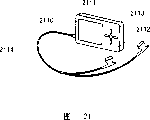
图21为说明根据本发明的电子设备的一例的图。FIG. 21 is a diagram illustrating an example of an electronic device according to the present invention.
具体实施方式Detailed ways
下面,关于本发明的实施方式将参照附图给予说明。但是,本发明可能通过多种不同的方式来实施,所属领域的普通人员可以很容易地理解一个事实就是其方式和详细内容可以被变换为各种各样的形式,而不脱离本发明的宗旨及其范围。例如,本实施方式和本实施例可以适当地组合来实施本发明。因此,本发明不应该被解释为仅限定在实施方式所记载的内容中。Hereinafter, embodiments of the present invention will be described with reference to the drawings. However, the present invention may be implemented in many different ways, and those skilled in the art can easily understand that the mode and details can be changed into various forms without departing from the spirit of the present invention. and its scope. For example, this embodiment mode and this example can be appropriately combined to implement the present invention. Therefore, the present invention should not be interpreted as being limited only to the contents described in the embodiments.
实施方式1Embodiment 1
在本实施方式中,将参照图1A和1B说明TFT的制造步骤,所述TFT中将通过LRTA改善了结晶性的氧化物半导体膜的一部分的区域用作沟道形成区域。In this embodiment mode, manufacturing steps of a TFT in which a region of a part of an oxide semiconductor film whose crystallinity is improved by LRTA is used as a channel formation region will be described with reference to FIGS. 1A and 1B .
首先,在衬底101上形成基底膜102。作为衬底101,可以使用聚对苯二甲酸乙二醇酯(PET)、聚萘二甲酸乙二醇酯(PEN)、聚醚砜(PES)、丙烯酸、以及聚酰亚胺等的塑料(合成树脂)或玻璃。First,
作为基底膜102,使用氧化硅膜、氮化硅膜、氧氮化硅膜(SiOxNy)(x>y)或氮氧化硅膜(SiNxOy)(x>y)等的绝缘膜的单层或叠层。通过溅射法或CVD法等形成基底膜102即可。注意,虽然可以不提供,然而在本发明中优选形成基底膜102。通过形成基底膜102,可以抑制从形成在基底膜102上的电极或布线等产生的热量传递到衬底101一侧。作为基底膜102,例如可以使用膜厚度为10至400nm的氮氧化硅膜。随后,在基底膜102上形成栅极103。As the
通过溅射法形成膜厚度为100至200nm的栅极103即可。此外,可以使用选自钽(Ta)、钨(W)、钛(Ti)、钼(Mo)、铬(Cr)、以及铌(Nb)等的元素、以上述元素为主要成分的合金材料或化合物材料来形成栅极103。此外,栅极103还可以由以掺杂有磷等杂质元素的多晶硅为典型的半导体材料形成。It is sufficient to form the
接着,以50至500nm左右的膜厚度形成覆盖栅极103的栅极绝缘膜104。作为栅极绝缘膜104,通过溅射法或各种CVD法如等离子体CVD法等单独或层叠形成含有硅的氧化物或硅的氮化物的膜。具体地,以单层结构形成含有氧化硅的膜(SiOx)、含有氧氮化硅的膜(SiOxNy)、含有氮氧化硅的膜(SiNxOy),或者,适当地层叠上述膜来形成。此外,还可以通过在含有氧、氮、或氧和氮的气氛中对栅极103进行高密度等离子体处理,使栅极103的表面氧化或氮化,以形成栅极绝缘膜。通过高密度等离子体处理而形成了的栅极绝缘膜优异于膜厚度和膜质量等的均匀性并且可以形成致密的膜。作为含氧的气氛,可以使用氧(O2)、二氧化氮(NO2)或一氧化二氮(N2O)与稀有气体的混合气体;或者,氧(O2)、二氧化氮(NO2)或一氧化二氮(N2O)与稀有气体、以及氢(H2)的混合气体。此外,作为含氮的气氛,可以使用氮(N2)或氨(NH3)与稀有气体的混合气体;或者,氮(N2)或氨(NH3)与稀有气体、以及氢(H2)的混合气体。可以由高密度等离子体所生成的氧基(有时包括OH基)或氮基(有时包括NH基)使栅极103的表面氧化或氮化。Next, the
当进行高密度等离子体处理形成栅极绝缘膜104时,以覆盖栅极103地形成厚度为1至20nm,优选为5至10nm的绝缘膜。这种情况下的反应是固相反应,因此可以极度降低该栅极绝缘膜104和栅极103之间的界面态密度。此外,由于栅极103直接被氧化或氮化,所以可以使被形成的栅极绝缘膜104的厚度均匀。就是说,通过这里所示的高密度等离子体处理使电极的表面固相氧化,可以形成具有良好均匀性和低界面态密度的绝缘膜。这里,选自钽(Ta)、钨(W)、钛(Ti)、钼(Mo)、铬(Cr)、以及铌(Nb)等的元素、以上述元素为主要成分的合金材料或化合物材料的氧化物用作栅极绝缘膜104。When the high-density plasma treatment is performed to form the
注意,栅极绝缘膜104可以仅仅使用通过高密度等离子体处理形成的绝缘膜,还可以通过利用等离子体或热反应的CVD法层叠包含氧化硅、含氧的氮化硅、含氮的氧化硅等的另一个绝缘膜中的至少一个。在哪一种情况下,当将晶体管制成其具有的栅极绝缘膜的一部分或全部包含通过高密度等离子体形成的绝缘膜时,可以减少特性的不均匀性。Note that for the
此外,栅极绝缘膜104可以使用与氧化物半导体膜的匹配性良好的氧化铝(Al2O3)、氮化铝(AlN)、氧化钛(TiO2)、氧化锆(ZrO2)、氧化锂(Li2O)、氧化钾(K2O)、氧化钠(Na2O)、氧化铟(In2O3)、氧化钇(Y2O3)、锆酸钙(CaZrO3)或至少含有上述材料中的两种的材料,也可以单独形成或者层叠两层或更多层来形成。In addition, aluminum oxide (Al 2 O 3 ), aluminum nitride (AlN), titanium oxide (TiO 2 ), zirconium oxide (ZrO 2 ), oxide Lithium (Li 2 O), potassium oxide (K 2 O), sodium oxide (Na 2 O), indium oxide (In 2 O 3 ), yttrium oxide (Y 2 O 3 ), calcium zirconate (CaZrO 3 ) or at least A material containing two of the above materials may also be formed alone or by laminating two or more layers.
接着,在栅极绝缘膜104上膜厚度成为50至200nm地形成布线105。作为布线材料,使用银(Ag)、铝(Al)、金(Au)、铜(Cu)、以及它们的合金等。只要比用于栅极103的材料反射率高就可以用作布线材料,通过考虑到与栅极103的关系而适当地组合来使用。布线可以层叠而形成,例如,可以采用从衬底一侧层叠铝和钛的布线。钛对使氧化物半导体膜和铝的电接触特性良好很有效。钛还具有抑制铝扩散到氧化物半导体膜中的功能。此外,布线还可以由透明导电膜形成,例如铟锡氧化物(ITO:Indium Tin Oxide)、含有氧化硅的铟锡氧化物(ITSO)、铟锌氧化物(IZO:Indium Zinc Oxide)、氧化铟(In2O3)、氧化锡(SnO2)、氧化锌(ZnO)、添加有铝的氧化锌(AlZnO)、添加有镓的氧化锌(GaZnO)、氧化锌(ZnO)等。注意,作为布线105优选使用对灯光的反射率比栅极103高或透光率比它高(或者,热吸收率比它低)的材料。Next, wiring 105 is formed on
接下来,在栅极绝缘膜104和布线105上形成氧化物半导体膜106。作为氧化物半导体膜106可以使用如下状态的氧化锌(ZnO),即非晶(非晶质的)状态、多晶状态、或非晶状态和多晶状态同时存在的微晶(也称作微晶体)状态,所述氧化锌中添加有元素周期表中第一族元素(例如,锂(Li)、钠(Na)、钾(K)、铷(Rb)、铯(Cs))、第十三族元素(例如,硼(B)、镓(Ga)、铟(In)、铊(Tl))、第十四族元素(例如,碳(C)、硅(Si)、锗(Ge)、锡(Sn)、铅(Pb))、第十五族元素(例如,氮(N)、磷(P)、砷(As)、锑(Sb)、铋(Bi))或第十七族元素(例如,氟(F)、氯(Cl)、溴(Br)、碘(I))等杂质元素中的一种或多种,或者,还可以使用什么杂质元素都没添加有的氧化锌。此外,还可以使用氧化钛(TiO2)、InGaO3(ZnO)5、氧化镁锌(MgxZn1-xO)、氧化镉锌(CdxZn1-xO)、氧化镉(CdO)、以及In-Ga-Zn-O之类的非晶氧化物半导体(a-IGZO)中的任何一种。氧化物半导体膜106以25至200nm(优选以30至150nm)的厚度在0.4Pa的压强下并且以Ar(氩)∶O2=50∶5sccm的流量的条件下通过溅射法淀积,然后,使用稀释到0.05%的氢氟酸通过蚀刻来形成为所希望的图形。与使用非晶硅膜的半导体膜相比,氧化物半导体膜106由于不会被氧化并且不在高真空中也可以形成,从而工序很廉价。此外,包含氧化锌的氧化物半导体膜由于难受到等离子体的影响,所以还可以使用等离子体CVD(也称作PCVD或PECVD)法淀积。在CVD法的装置中,等离子体CVD法的装置尤其简单,而且其生产率也高。Next, an
接着,对衬底101的背面进行LRTA(图1A)。LRTA以250至570℃(优选以300至400℃,更优选以300至350℃)进行1分钟至1小时,优选进行10分钟至30分钟。通过来自选自卤素灯、金属卤化物灯、氙弧灯、炭弧灯、高压钠灯、以及高压汞灯中的一种或多种的辐射进行LRTA。通过LRTA法可以以短时间进行热处理,所以只要布线105的反射率或透过率比栅极103高就可以使用熔点较低的材料。具有红外光区域、可见光区域、紫外光区域等的波长的光可以用于LRTA法。注意,可以使用激光束代替LRTA来进行加热处理,例如,可以使用红外光激光、可见光激光、紫外光激光等作为激光束。此外,可以组合LRTA和激光束辐照来选择性地改善氧化物半导体膜的结晶性。在使用激光辐照的情况下,可以使用连续振荡型激光束(CW激光束)和脉冲振荡型激光束(脉冲激光束)。作为这里可以使用的激光束,可以使用由如下激光器的一种或多种振荡的激光束:气体激光器如Ar激光器、Kr激光器、受激准分子激光器等;以将Nd、Yb、Cr、Ti、Ho、Er、Tm和Ta中的一种或多种作为掺杂剂添加的单晶YAG、YVO4、镁橄榄石(Mg2SiO4)、YAlO3、GdVO4、或者多晶(陶瓷)YAG、Y2O3、YVO4、YAlO3、GdVO4作为介质的激光器;玻璃激光器;红宝石激光器;变石激光器;Ti:蓝宝石激光器;铜蒸汽激光器;或者金蒸汽激光器。通过照射上述激光束的基波以及该基波的第二至第四高次谐波的激光束,可以使结晶性良好。注意,作为激光束优选使用其能量比氧化物半导体膜的带隙大的激光束。例如可以使用由KrF、ArF、XeCl或XeF的受激准分子激光振荡器发射的激光束。Next, LRTA is performed on the back surface of the substrate 101 (FIG. 1A). LRTA is performed at 250 to 570°C (preferably at 300 to 400°C, more preferably at 300 to 350°C) for 1 minute to 1 hour, preferably for 10 minutes to 30 minutes. LRTA is performed by radiation from one or more selected from a halogen lamp, a metal halide lamp, a xenon arc lamp, a carbon arc lamp, a high pressure sodium lamp, and a high pressure mercury lamp. The heat treatment can be performed in a short time by the LRTA method, so as long as the reflectance or transmittance of the
此时,栅极103由与布线105相比对灯光的反射率低且吸收更大的热量的材料形成,从而栅极103加热到比布线105更高的温度。由此,栅极103周围的氧化物半导体膜106被加热,以形成第二氧化物半导体区域108和第一氧化物半导体区域107,该第一氧化物半导体膜107的结晶性比第二氧化物半导体区域108良好(参照图1B)。这里,使用卤素灯对栅极103照射灯光使它加热到约300℃,并且利用其热量使氧化物半导体膜106结晶化来改善结晶性。此时,由于将对灯光的反射率或透过率比栅极103高的材料用于布线105,所以即使在使氧化物半导体膜106结晶化,布线105的温度也成为300℃或更低。At this time, the
这里,将用作氧化物半导体膜的ZnO的结晶性的热处理温度依赖性示出于图2。图2示出在以下情况下测定了(002)面的X射线的强度的结果,即喷射流量为Ar∶O2=50∶5(sccm)的比例的成膜气体的状态(as-depo);以200℃、300℃、350℃各个温度加热1小时的情况。随着热处理温度的上升,(002)面的强度高峰变大。由此,至少直到350℃,热处理温度越高ZnO的结晶性也越高。一般来说,由于结晶性越进展迁移率越高,所以热处理优选以350℃左右进行。注意,若衬底没有闪烁等问题,就可以进行ZnO达到400℃左右的热处理。Here, the heat treatment temperature dependence of the crystallinity of ZnO used as an oxide semiconductor film is shown in FIG. 2 . Fig. 2 shows the results of measuring the intensity of X-rays on the (002) plane, that is, the state (as-depo) of the film-forming gas whose injection flow rate is Ar:O 2 =50:5 (sccm) ;The case of heating at each temperature of 200°C, 300°C, and 350°C for 1 hour. As the heat treatment temperature rises, the strength peak of the (002) plane becomes larger. Therefore, at least up to 350° C., the higher the heat treatment temperature, the higher the crystallinity of ZnO. In general, the heat treatment is preferably performed at about 350° C. because the crystallinity progresses and the mobility increases. Note that if the substrate does not have problems such as flashing, ZnO can be heat-treated to reach about 400°C.
另一方面,在图1A中,与形成有栅极103或布线105的区域相比,没形成有栅极103和布线105的区域,即层叠有衬底101、基底膜102、栅极绝缘膜104、以及氧化物半导体膜106的区域中灯光容易透过,从而该区域不容易吸收热量,其加热温度比布线105低。因此,衬底101的大部分区域为350℃或更低,所以不容易产生收缩。注意,没形成有栅极103的区域越大,抑制衬底101收缩的效果越大。On the other hand, in FIG. 1A, compared with the region where the
接着,通过在氧化物半导体膜106上形成层间绝缘膜、源电极、漏极、像素电极、发光元件等结构来形成半导体器件。Next, a semiconductor device is formed by forming an interlayer insulating film, a source electrode, a drain electrode, a pixel electrode, a light emitting element, and the like on the
在本发明中,在使用ZnO作为半导体的情况下,由于可以以300℃左右的热处理温度改善ZnO层的结晶性,所以与使用结晶硅膜作为半导体膜的情况相比,可以抑制热处理温度。另外,由于使用透光性高的氧化物半导体膜并通过LRTA选择性地加热栅极,从而可以抑制衬底的闪烁,而不使衬底的大部分被加热。此外,由于将对灯光的反射率比栅极高的材料用于布线,即使在将加热布线的温度抑制为350℃左右,也可以改善氧化物半导体膜的结晶性。由此,可以使用熔点低的Al布线。此外,可以防止氧化物半导体膜中的氧气扩散在Al中而形成绝缘膜。Al布线很廉价且低电阻,从而可以以低成本并且良好生产率来制造功能好的半导体器件。In the present invention, when ZnO is used as a semiconductor, the crystallinity of the ZnO layer can be improved at a heat treatment temperature of about 300° C., so that the heat treatment temperature can be suppressed compared with the case of using a crystalline silicon film as a semiconductor film. In addition, by using a highly transparent oxide semiconductor film and selectively heating the gate by LRTA, flickering of the substrate can be suppressed without heating most of the substrate. In addition, since the wiring is made of a material that has a higher reflectance to light than that of the gate electrode, the crystallinity of the oxide semiconductor film can be improved even when the temperature for heating the wiring is suppressed to about 350°C. Accordingly, Al wiring with a low melting point can be used. In addition, oxygen in the oxide semiconductor film can be prevented from diffusing into Al to form an insulating film. Al wiring is cheap and has low resistance, so that a functional semiconductor device can be manufactured at low cost and with good productivity.
实施方式2Embodiment 2
在本实施方式中,将使用图3A至3C说明与实施方式1不同的结构。注意,至在衬底301上形成基底膜302、栅极303、以及栅极绝缘膜304的步骤,参照实施方式1所示的至在衬底101上形成基底膜102、栅极103、以及栅极绝缘膜104的步骤而进行。In this embodiment mode, a structure different from Embodiment Mode 1 will be described using FIGS. 3A to 3C . Note that up to the steps of forming the
在栅极绝缘膜304上形成第一氧化物半导体膜305。作为氧化物半导体膜305可以使用三种状态的添加有元素周期表中第一族元素、第十三族元素、第十四族元素、第十五族元素或第十七族元素等杂质元素中的一种或多种的氧化锌(ZnO)、或者什么杂质元素都没有添加的氧化锌,所述三种状态如下:非晶(非晶质)状态;多晶状态;以及非晶状态和多晶状态同时存在的微晶(也称作微晶体)状态。此外,还可以使用InGaO3(ZnO)5、氧化镁锌(MgxZn1-xO)、氧化镉锌(CdxZn1-xO)、氧化镉(CdO)、或In-Ga-Zn-O之类的非晶氧化物半导体(a-IGZO)中的任何一种。这里,通过溅射法以50至200nm(优选以100至150nm)的厚度形成第一氧化物半导体膜305。A first
接下来,从衬底表面进行LRTA,以便使结晶性良好(图3A)。LRTA以250至570℃(优选以300至400℃,更优选以300至350℃)进行1分钟至1小时,更优选进行10至30分钟即可,并且通过从选自卤素灯、金属卤化物灯、氙弧灯、炭弧灯、高压钠灯、以及高压汞灯中的一种或多种的辐射来进行。在本实施方式中,在氧气氛中进行30分钟的灯加热,以便使栅极303达到约300℃,以使中间夹着栅极绝缘膜304与栅极303重叠的第一氧化物半导体膜305的区域提高结晶性。因为第一氧化物半导体膜305具有透光性,所以通过优先加热栅极303,第一氧化物半导体膜305的结晶性从栅极303的周围向外侧提高。于是,如图3B所示,第二氧化物半导体膜被形成,该第二氧化物半导体膜包括第二氧化物半导体区域309以及比第二氧化物半导体区域309结晶性良好的第一氧化物半导体区域308。注意,在图3A中虽然从衬底301的表面一侧进行灯加热,然而还可以从衬底背面进行LRTA。因为氧化物半导体膜305具有透光性,所以即使进行LRTA,衬底的大部分区域也不容易加热。由此,如果使用熔点低的树脂等作为衬底,也可以抑制由衬底的缩小等导致的变形。注意,还可以通过提高LRTA的输出功率从衬底表面进行灯加热,而直接改善氧化物半导体膜表面附近的结晶性。此外,通过调节灯光的波长、栅极的反射率、以及氧化物半导体膜的膜厚度,当从衬底的表面进行灯加热时,在栅极反射的灯光在氧化物半导体膜的栅极绝缘膜304一侧的表面附近被吸收,使得与栅极重叠的氧化物半导体膜的栅极绝缘膜304一侧的表面附近被优先结晶化。此外,在使用玻璃衬底作为衬底的情况下,灯光利用从可见光至红外光的区域。这种波长区域的光不容易被玻璃衬底吸收,从而可以将玻璃衬底的加热限度抑制得最小。灯加热可以多次进行。通过多次进行,可以在抑制衬底温度的上升的同时以长时间加热栅极。Next, LRTA is performed from the substrate surface in order to make the crystallinity good (FIG. 3A). LRTA is carried out at 250 to 570°C (preferably at 300 to 400°C, more preferably at 300 to 350°C) for 1 minute to 1 hour, more preferably for 10 to 30 minutes, and is selected from halogen lamps, metal halides Radiation of one or more of lamps, xenon arc lamps, carbon arc lamps, high pressure sodium lamps, and high pressure mercury lamps is performed. In this embodiment mode, lamp heating is performed in an oxygen atmosphere for 30 minutes so that the
注意,还可以代替LRTA而照射激光束或紫外光,或者组合它们选择性的改善氧化物半导体膜的结晶性。在使用激光辐照的情况下,可以使用连续振荡型激光束(CW激光束)和脉冲振荡型激光束(脉冲激光束)。作为这里可以使用的激光束,可以使用由如下激光器的一种或多种振荡的激光束:气体激光器如Ar激光器、Kr激光器、受激准分子激光器等;以将Nd、Yb、Cr、Ti、Ho、Er、Tm和Ta中的一种或多种作为掺杂剂添加的单晶YAG、YVO4、镁橄榄石(Mg2SiO4)、YAlO3、GdVO4、或者多晶(陶瓷)YAG、Y2O3、YVO4、YAlO3、GdVO4作为介质的激光器;玻璃激光器;红宝石激光器;变石激光器;Ti:蓝宝石激光器;铜蒸汽激光器;或者金蒸汽激光器。通过照射上述激光束的基波以及该基波的第二至第四高次谐波的激光束,可以使结晶性良好。注意,作为激光束优选使用其能量比氧化物半导体膜的带隙大的激光束。例如可以使用由KrF、ArF、XeCl或XeF的受激准分子激光震荡器发射的激光束。Note that it is also possible to selectively improve the crystallinity of the oxide semiconductor film by irradiating a laser beam or ultraviolet light instead of LRTA, or combining them. In the case of using laser irradiation, a continuous oscillation type laser beam (CW laser beam) and a pulse oscillation type laser beam (pulse laser beam) can be used. As the laser beam usable here, laser beams oscillated by one or more of the following lasers can be used: gas lasers such as Ar lasers, Kr lasers, excimer lasers, etc.; to combine Nd, Yb, Cr, Ti, Single crystal YAG, YVO 4 , forsterite (Mg 2 SiO 4 ), YAlO 3 , GdVO 4 , or polycrystalline (ceramic) YAG with one or more of Ho, Er, Tm and Ta added as a dopant , Y 2 O 3 , YVO 4 , YAlO 3 , GdVO 4 as a medium laser; glass laser; ruby laser; alexandrite laser; Ti: sapphire laser; copper vapor laser; or gold vapor laser. The crystallinity can be improved by irradiating the fundamental wave of the above-mentioned laser beam and the laser beams of the second to fourth harmonics of the fundamental wave. Note that a laser beam whose energy is larger than the band gap of the oxide semiconductor film is preferably used as the laser beam. For example, a laser beam emitted from an excimer laser oscillator of KrF, ArF, XeCl, or XeF can be used.
接着,通过溅射法在第一氧化物半导体区域308和第二氧化物半导体区域309上按顺序沉积Ti和Al,以形成Ti层和Al层。然后,通过使用光刻法和Cl2气体对Ti和Al层进行干蚀刻,形成成为源极布线和漏极布线的布线306和布线307(图3C)。在加速电压为1.5kW、压强为0.4Pa的情况下使用Ar(流量为30sccm)以10至200nm的膜厚度形成布线306和307。注意,虽然层叠形成布线306和307,然而只要使用与氧化物半导体膜305的匹配性好的材料,就可以单独形成布线306和307。作为布线306和307可以适当地使用铝(Al)、钨(W)、钼(Mo)、锆(Zr)、铪(Hf)、钒(V)、铌(Nb)、钽(Ta)、铬(Cr)、钴(Co)、镍(Ni)、铂(Pt)、钛(Ti)、钕(Nd)等的金属、上述金属的合金或其金属氮化物、铟锡氧化物(ITO)、铟锌氧化物(IZO)、包含氧化硅的铟锡氧化物(ITSO)、氧化铟(In2O3)、氧化锡(SnO2)、氧化锌(ZnO)、添加有铝的氧化锌(AlZnO)、或添加有镓的氧化锌(GaZnO)等的具有透光性的材料。Next, Ti and Al are sequentially deposited on the first
之后,在氧化物半导体膜305、布线306、以及布线307上形成层间绝缘膜、布线、像素电极、发光元件等的结构,以制造半导体器件。After that, a structure of an interlayer insulating film, wiring, pixel electrodes, light-emitting elements, and the like is formed on the
在本实施方式中,在对氧化物半导体膜305进行LRTA来改善结晶性之后形成布线。因此,布线306可以使用对灯光的反射率比栅极303低的材料并且其材料不局限于实施方式1所述的材料,只要是与氧化物半导体膜305的匹配性好的材料即可。In the present embodiment, wiring is formed after LRTA is performed on the
注意,通过LRTA的加热在形成氧化物半导体膜305之后使它加工成所要求的形状之前或使它加工成所要求的形状之后都可以进行。Note that the heating by LRTA may be performed either after forming the
在本发明中,当使用氧化锌作为半导体膜时以300℃左右的热处理温度改善半导体膜的结晶性,所以与使用结晶硅膜作为半导体膜的情况相比可以抑制热处理温度,从而可以以低成本进行结晶化步骤。此外,本发明由于使用透光性高的氧化物半导体膜通过LRTA选择性的加热栅极,所以衬底的大部分没有被加热,以可以抑制衬底的收缩。In the present invention, when zinc oxide is used as the semiconductor film, the crystallinity of the semiconductor film is improved at a heat treatment temperature of about 300° C., so that the heat treatment temperature can be suppressed compared with the case of using a crystalline silicon film as the semiconductor film, thereby enabling low-cost A crystallization step is performed. In addition, in the present invention, since the gate is selectively heated by the LRTA using a highly transparent oxide semiconductor film, most of the substrate is not heated, and shrinkage of the substrate can be suppressed.
实施方式3Embodiment 3
将参照图4A至5C说明本发明的实施方式。本实施方式为具有沟道保护型的薄膜晶体管的半导体器件的例子。Embodiments of the present invention will be described with reference to FIGS. 4A to 5C . This embodiment mode is an example of a semiconductor device including a channel protection type thin film transistor.
作为衬底400,使用由硼硅酸钡玻璃、硼硅酸铝玻璃等构成的玻璃衬底、硅衬底、具有耐热性的塑料衬底或树脂衬底。作为塑料衬底或树脂衬底,可以使用聚对苯二甲酸乙二醇酯(PET)、聚萘二甲酸乙二醇酯(PEN)、聚醚砜(PES)、丙烯酸、聚酰亚胺等。此外,可以通过CMP法等抛光衬底400的表面,以使它平坦化。还可以在衬底400上形成绝缘层。绝缘层通过CVD法、等离子体CVD法、溅射法、旋转涂敷法等已知的方法使用含硅的氧化物材料、氮化物材料的至少一种由单层或叠层形成。可以不形成该绝缘层,然而,该绝缘层具有遮断来自衬底400的污染物质的效果以及抑制热量传到衬底的效果。As the
在衬底400上形成导电膜401。导电膜401被加工成所要求的形状,而成为栅极。导电膜401优选通过印刷法、电场电镀法、蒸发沉积法等的方法使用对用于LRTA加热的光源的波长的反射率低(容易吸收热量,即容易被加热)的材料形成。通过使用反射率低的材料,可以进行之后的加热步骤。作为导电膜401,可以适当地使用金属如钨(W)、钼(Mo)、锆(Zr)、铪(Hf)、钒(V)、铌(Nb)、钽(Ta)、铬(Cr)、钴(Co)、镍(Ni)、铂(Pt)、钛(Ti)、钕(Nd)等;它们的合金;或它们的金属氮化物。此外,还可以层叠上述材料的多个层形成导电膜401。典型地是,可以在衬底表面上形成氮化钽膜,并且在其上层叠钨膜。此外,还可以使用在硅中添加赋予一个导电类型的杂质元素的材料。例如,可以使用具有n型的硅膜等,该硅膜包含如磷(P)等赋予n型的杂质元素。导电膜401以10至200nm的膜厚度形成。A
在本实施方式中,通过溅射法使用钨(W)形成膜厚度为150nm的导电膜401。In this embodiment mode, the
使用光刻步骤在导电膜401上形成由抗蚀剂构成的掩模,并且使用该掩模将导电膜401加工成所要求的形状,以形成栅极402(参照图4B)。A mask made of resist is formed on the
接着,在栅极402上形成栅极绝缘膜403a和栅极绝缘膜403b,以形成两层的叠层结构。优选地,通过在保持真空状态下改变反应气体,在同一容器内且相同的温度下,连续叠层来形成绝缘层。当在保持真空状态下连续地形成时,可以防止要叠层的膜之间的界面受到污染。Next, a
栅极绝缘膜403a和栅极绝缘膜403b可以适当地使用氧化硅(SiOx)、氮化硅(SiNx)、氧氮化硅(SiOxNy)(x>y)、氮氧化硅(SiNxOy)(x>y)等。再者,可以使栅极402氧化来形成氧化膜而代替栅极绝缘膜403a。注意,优选使用氮化硅(SiNx)、氮氧化硅(SiNxOy)(x>y)等形成栅极绝缘膜403a,以便防止杂质等从衬底一侧扩散。此外,优选使用氧化硅(SiOx)、氧氮化硅(SiOxNy)(x>y)形成栅极绝缘膜403b。注意,为了以低成膜温度形成栅极漏电流少的致密的绝缘膜,优选将氩等稀有气体元素包含在反应气体中,以使它混入在要形成的绝缘膜中。在本实施方式中,使用SiH4和NH3作为反应气体以50至140nm的膜厚度由氮化硅膜形成栅极绝缘膜403a,并且使用SiH4和N2O作为反应气体以100nm的膜厚度由氧化硅膜层叠形成栅极绝缘膜403b。注意,优选将栅极绝缘膜403a和栅极绝缘膜403b的膜厚度分别设定为50至100nm。For the
此外,栅极绝缘膜403b可以由与之后要形成的氧化物半导体膜的匹配性良好的氧化铝(Al2O3)或氮化铝(AlN)形成。在此情况下,通过使用绝缘性高的氧化硅、氮化硅、氧氮化硅、氮氧化硅等作为栅极绝缘膜403a,并且使用与氧化物半导体膜的界面特性好的氧化铝或氮化铝作为栅极绝缘膜403b,可以形成可靠性高的栅极绝缘膜。注意,还可以将栅极绝缘膜形成为三层,并且将第三层作为使用氧化铝或氮化铝的栅极绝缘膜。In addition, the
接着,在栅极绝缘膜403b上形成氧化物半导体膜404。通过溅射法在流量为Ar∶O2=50∶5(sccm)、压强为0.4Pa的情况下以100nm的膜厚度形成氧化物半导体膜404。Next, an
作为氧化物半导体膜404可以使用三种状态的添加有元素周期表中第一族元素、第十三族元素、第十四族元素、第十五族元素或第十七族元素等杂质元素中的一种或多种的氧化锌(ZnO)、或者什么杂质元素都没有添加的氧化锌,所述三种状态如下:非晶(非晶质)状态;多晶状态;以及非晶状态和多晶状态同时存在的微晶(也称作微晶体)状态。此外,还可以使用氧化钛(TiO2)、InGaO3(ZnO)5、氧化镁锌(MgxZn1-xO)、氧化镉锌(CdxZn1-xO)、氧化镉(CdO)、或In-Ga-Zn-O之类的非晶氧化物半导体(a-IGZO)中的任何一种。As the
注意,在将ZnO用作氧化物半导体膜404的情况下,优选掺杂氮。ZnO本来呈现n型半导体的性质。通过添加氮,氮对ZnO起受主杂质的作用,结果可以控制阈值电压。Note that in the case of using ZnO as the
接着,使用LRTA法从衬底400的表面或背面进行对氧化物半导体膜404的加热(图4D)。LRTA通过从选自卤素灯、氙弧灯、金属卤化物灯、炭弧灯、高压钠灯、以及高压汞灯中的一种或多种的辐射来进行。LRTA以250至570℃(优选以300至400℃,更优选以300至350℃)进行1分钟至1小时,优选进行10至30分钟。在本实施方式,以卤素灯为光源在氧气氛中并且在300℃、30分钟的条件下进行灯加热。Next, the
通过进行LRTA,以短时间选择性地加热栅极402,在形成在栅极402周围的用虚线所示的区域434中由加热的热量形成结晶性提高了的第一氧化物半导体区域。另一方面,在用虚线所示的区域434之外的区域424中很少吸收灯光,从而该区域几乎没有被加热,以形成结晶性与第一氧化物半导体区域不同的第二氧化物半导体区域(图4E)。因此,仅仅形成有栅极402的区域被选择性地加热,而其它区域没有被加热,从而可以抑制衬底400的缩小和弯曲。注意,通过提高LRTA的输出功率从衬底表面进行灯加热,而直接改善氧化物半导体膜表面附近的结晶性。此外,还可以通过调节灯光的波长、栅极的反射率、以及氧化物半导体膜的膜厚度,当从衬底的表面进行灯加热时,在栅极反射的灯光在氧化物半导体膜的栅极绝缘膜403b一侧的表面附近被吸收,以与栅极重叠的氧化物半导体膜的栅极绝缘膜403b一侧的表面附近被优先结晶化。此外,在使用玻璃衬底作为衬底的情况下,灯光利用从可见光至红外光的区域。这种波长区域的光不容易被玻璃衬底吸收,从而可以将玻璃衬底的加热限度抑制得最小。注意,灯加热可以多次进行。通过多次进行,可以在抑制衬底温度的上升的同时以长时间加热栅极。By performing LRTA, the
注意,还可以代替LRTA而照射激光束或紫外光,或者组合它们选择性的改善氧化物半导体膜的结晶性。在使用激光辐照的情况下,可以使用连续振荡型激光束(CW激光束)和脉冲振荡型激光束(脉冲激光束)。作为这里可以使用的激光束,可以使用由如下激光器的一种或多种振荡的激光束:气体激光器如Ar激光器、Kr激光器、受激准分子激光器等;以将Nd、Yb、Cr、Ti、Ho、Er、Tm和Ta中的一种或多种作为掺杂剂添加的单晶YAG、YVO4、镁橄榄石(Mg2SiO4)、YAlO3、GdVO4、或者多晶(陶瓷)YAG、Y2O3、YVO4、YAlO3、GdVO4作为介质的激光器;玻璃激光器;红宝石激光器;变石激光器;Ti:蓝宝石激光器;铜蒸汽激光器;或者金蒸汽激光器。通过照射上述激光束的基波以及该基波的第二至第四高次谐波的激光束,可以使结晶性良好。注意,作为激光束优选使用其能量比氧化物半导体膜的带隙大的激光束。例如可以使用由KrF、ArF、XeCl或XeF的受激准分子激光振荡器发射的激光束。Note that it is also possible to selectively improve the crystallinity of the oxide semiconductor film by irradiating a laser beam or ultraviolet light instead of LRTA, or combining them. In the case of using laser irradiation, a continuous oscillation type laser beam (CW laser beam) and a pulse oscillation type laser beam (pulse laser beam) can be used. As the laser beam usable here, laser beams oscillated by one or more of the following lasers can be used: gas lasers such as Ar lasers, Kr lasers, excimer lasers, etc.; to combine Nd, Yb, Cr, Ti, Single crystal YAG, YVO 4 , forsterite (Mg 2 SiO 4 ), YAlO 3 , GdVO 4 , or polycrystalline (ceramic) YAG with one or more of Ho, Er, Tm and Ta added as a dopant , Y 2 O 3 , YVO 4 , YAlO 3 , GdVO 4 as a medium laser; glass laser; ruby laser; alexandrite laser; Ti: sapphire laser; copper vapor laser; or gold vapor laser. The crystallinity can be improved by irradiating the fundamental wave of the above-mentioned laser beam and the laser beams of the second to fourth harmonics of the fundamental wave. Note that a laser beam whose energy is larger than the band gap of the oxide semiconductor film is preferably used as the laser beam. For example, a laser beam emitted from an excimer laser oscillator of KrF, ArF, XeCl, or XeF can be used.
接着,在氧化物半导体膜404上形成保护膜405,并且在保护膜405上形成抗蚀剂406(参照图4F)。将抗蚀剂406作为掩模通过光刻步骤将保护膜405加工成所要求的形状,以形成沟道保护膜407。作为沟道保护膜可以适当地使用氧化硅(SiOx)、氮化硅(SiNx)、氧氮化硅(SiOxNy)(x>y)、氮氧化硅(SiNxOy)(x>y)等。通过形成沟道保护膜407,当形成源极层和漏极层时可以防止沟道部的半导体层被蚀刻。在本实施方式中,形成氮化硅膜作为保护膜405,以形成沟道保护膜407(参照图4G)。Next, a
接着,使用光刻步骤由抗蚀剂制作掩模408(图4H),并且使用该掩模408对氧化物半导体膜404进行蚀刻,以形成被加工成所要求的形状的氧化物半导体膜409(也称作岛状氧化物半导体膜)(图5A)。注意,对蚀刻使用稀释了的氢氟酸。之后,在氧化物半导体膜409上形成第一导电膜411和第二导电膜412,并且使用光刻步骤由抗蚀剂形成掩模413(图5B)。使用掩模413将第一导电膜411和第二导电膜412加工成所要求的形状,形成用作源电极或漏极的第一导电膜414a和414b以及第二导电膜415a和415b(图5C)。Next, a
作为掩模可以使用包含感光剂的市场上销售的抗蚀剂材料,例如可以使用作为典型的正性抗蚀剂的酚醛树酯、作为感光剂的萘醌二叠氮化物、作为负性抗蚀剂的基托树脂、二苯基硅二醇、以及产酸剂等。使用任何材料,其表面张力和粘度该通过调整溶剂的浓度或加界面激活剂等而适当地调整。此外,当使用包含具有感光性的感光物质的导电材料作为导电膜时,即使不形成由抗蚀剂构成的掩模,也通过直接对导电膜照射激光束,并且由曝光和蚀刻剂进行去除,而可以加工成所要求的形状。在此情况下,可以不形成掩模,从而有步骤简单化的优点。As a mask, a commercially available resist material containing a photosensitive agent can be used, for example, a phenolic resin as a typical positive resist, naphthoquinone diazide as a photosensitive agent, and a negative photoresist can be used. agent base resin, diphenylsilanediol, and acid generators. Use any material whose surface tension and viscosity should be properly adjusted by adjusting the concentration of the solvent or adding a surface activator, etc. In addition, when using a conductive material containing a photosensitive material having photosensitivity as the conductive film, even without forming a mask made of resist, by directly irradiating the conductive film with a laser beam and removing it by exposure and etchant, And can be processed into the required shape. In this case, there is no need to form a mask, and there is an advantage of simplification of steps.
包含感光性物质的导电材料可以包括诸如Ag、Au、Cu、Ni、Al和Pt等金属或其合金以及感光性树脂,该感光树脂由有机高分子树脂、光重合起动剂、光重合单体或溶剂等构成。作为有机高分子树脂,使用酚醛清漆树脂、丙烯酸类共聚物、甲基丙烯酸类共聚物、纤维素衍生物、环化橡胶类树脂等。The conductive material containing the photosensitive substance may include metals such as Ag, Au, Cu, Ni, Al, and Pt or alloys thereof, and a photosensitive resin made of organic polymer resin, photopolymerization starter, photopolymerization monomer or solvent etc. As the organic polymer resin, novolac resins, acrylic copolymers, methacrylic copolymers, cellulose derivatives, cyclized rubber resins, and the like are used.
注意,在形成第一导电膜411之前,可以将例如由添加有铝的氧化锌(AlZnO)或添加有镓的氧化锌(GaZnO)构成的导电膜再一层形成在氧化物半导体膜404上而作为n型氧化物半导体。通过形成由AlZnO或GaZnO构成的导电膜,第一导电膜411和氧化物半导体膜409的匹配性良好,以可以降低源电极和漏极的接触电阻。此外,还可以采用在GaZnO上形成Ti或在Ti上形成GaZnO的层叠结构。Note that, before forming the first
此外,作为第一导电膜414a和414b以及第二导电膜415a和415b,可以适当地使用铝(Al)、钨(W)、钼(Mo)、锆(Zr)、铪(Hf)、钒(V)、铌(Nb)、钽(Ta)、铜(Cu)、铬(Cr)、钴(Co)、镍(Ni)、铂(Pt)、钛(Ti)、钕(Nd)等的金属或其合金,或者其金属氮化物。例如,可以考虑如下组合:第一导电膜为Ti,并且第二导电膜为Al;第一导电膜为Ta,并且第二导电膜为W;第一导电膜为TaN,并且第二导电膜为Al;第一导电膜为TaN,并且第二导电膜为Cu;以及第一导电膜为Ti,第二导电膜为Al,并且第三导电膜为Ti。第一层和第二层中的任一个可以由AgPdCu合金形成。而且,也可以采用按顺序层叠W、Al和Si的合金(Al-Si)、以及TiN的三层结构。可以使用氮化钨代替W,可以使用Al和Ti的合金膜(Al-Ti)代替Al和Si的合金(Al-Si),或者可以使用Ti代替TiN。为了改善耐热性,铝可以添加0.5至5原子%的元素,诸如钛、硅、钪、钕和铜等。Further, as the first conductive films 414a and 414b and the second conductive films 415a and 415b, aluminum (Al), tungsten (W), molybdenum (Mo), zirconium (Zr), hafnium (Hf), vanadium ( V), niobium (Nb), tantalum (Ta), copper (Cu), chromium (Cr), cobalt (Co), nickel (Ni), platinum (Pt), titanium (Ti), neodymium (Nd) and other metals Or its alloy, or its metal nitride. For example, the following combinations can be considered: the first conductive film is Ti, and the second conductive film is Al; the first conductive film is Ta, and the second conductive film is W; the first conductive film is TaN, and the second conductive film is Al; the first conductive film is TaN, and the second conductive film is Cu; and the first conductive film is Ti, the second conductive film is Al, and the third conductive film is Ti. Either of the first layer and the second layer may be formed of AgPdCu alloy. Furthermore, a three-layer structure in which W, an alloy of Al and Si (Al—Si), and TiN are stacked in this order may also be adopted. Tungsten nitride may be used instead of W, an alloy film of Al and Ti (Al—Ti) may be used instead of an alloy of Al and Si (Al—Si), or Ti may be used instead of TiN. In order to improve heat resistance, aluminum may be added with 0.5 to 5 atomic % of elements such as titanium, silicon, scandium, neodymium, and copper.
此外,作为形成第一导电膜411和第二导电膜412的导电材料,可以使用铟锡氧化物(ITO)、铟锌氧化物(IZO)、含有氧化硅的铟锡氧化物(ITSO)、氧化铟(In2O3)、氧化锡(SnO2)、氧化锌(ZnO)、氧化钛等的具有透光性的材料、以及适当组合它们的材料。In addition, as a conductive material for forming the first
注意,在本实施方式中,在对氧化物半导体膜305进行LRTA使它改善其结晶性之后,形成第一导电膜411和第二导电膜412。因此,第一导电膜411和第二导电膜412可以由比栅极402对灯光的反射率低的材料形成,用作布线或电极的导电材料只要与氧化物半导体膜305的匹配性好,就不局限于实施方式1中举出的材料。Note that, in this embodiment mode, the first
注意,在本实施方式中,蚀刻加工可以采用等离子体蚀刻(干蚀刻)或湿蚀刻的任一种,然而当处理大面积衬底时等离子体蚀刻更合适。作为蚀刻气体,使用CF4、NF3、SF6、CHF3等的氟类、以Cl2、BCl3、SiCl4或CCl4等为典型的氯类气体或者O2气体,还可以适当地添加He和Ar等的惰性气体。此外,如果应用大气压放电的蚀刻加工,就可以局部放电加工,从而无须在衬底的整个面上形成掩模层。Note that, in this embodiment mode, either plasma etching (dry etching) or wet etching may be used for the etching process, but plasma etching is more suitable when a large-area substrate is processed. As the etching gas, fluorine-based gases such as CF 4 , NF 3 , SF 6 , and CHF 3 , chlorine-based gases such as Cl 2 , BCl 3 , SiCl 4 , or CCl 4 , or O 2 gases can be used as appropriate. Inert gases such as He and Ar. In addition, if the etching process of the atmospheric pressure discharge is used, the partial discharge process can be performed, so that it is not necessary to form a mask layer on the entire surface of the substrate.
注意,在本实施方式的光刻步骤中,可以在涂敷抗蚀剂之前将膜厚度为几nm左右的绝缘膜形成在氧化物半导体膜的表面上。通过该步骤可以避免氧化物半导体膜和抗蚀剂直接接触,从而可以防止包含在抗蚀剂中的杂质进入在氧化物半导体膜中。Note that in the photolithography step of this embodiment mode, an insulating film having a film thickness of about several nm may be formed on the surface of the oxide semiconductor film before applying a resist. Through this step, direct contact between the oxide semiconductor film and the resist can be avoided, so that impurities contained in the resist can be prevented from entering the oxide semiconductor film.
通过上述步骤可以制造沟道部分的半导体层没有蚀刻的底栅型(也称作反交错型)的薄膜晶体管。注意,在本实施方式中虽然制造了底栅型TFT,然而只要将中间夹着栅极绝缘膜形成在提供在衬底上的氧化物半导体膜上的栅极通过LRTA加热,并且可以改善至少氧化物半导体膜的沟道形成区域的结晶性,就可以采用顶栅型TFT。Through the above steps, a bottom gate type (also referred to as an inverted staggered type) thin film transistor in which the semiconductor layer of the channel portion is not etched can be manufactured. Note that although a bottom-gate TFT is manufactured in this embodiment mode, as long as the gate formed on the oxide semiconductor film provided on the substrate with the gate insulating film interposed therebetween is heated by LRTA, at least oxidation can be improved. If the crystallinity of the channel formation region of the material semiconductor film is improved, a top-gate TFT can be used.
本实施方式可以与实施方式1和2适当地组合。This embodiment mode can be combined with Embodiment Modes 1 and 2 as appropriate.
实施方式4Embodiment 4
将使用图6A至6F对本发明的实施方式进行说明。本实施方式为在实施方式3中具有沟道蚀刻型薄膜晶体管的半导体器件的例子。由此,对于相同的部分或具有相同功能的部分省略其重复说明。Embodiments of the present invention will be described using FIGS. 6A to 6F . This embodiment mode is an example of a semiconductor device having a channel-etched thin film transistor in Embodiment Mode 3. FIG. Therefore, repeated descriptions of the same parts or parts having the same functions are omitted.
在衬底600上形成栅极层602,并且覆盖栅极层602地形成栅极绝缘膜603a和栅极绝缘膜603b(参照图6A)。在栅极绝缘膜603b上形成氧化物半导体膜,并且形成具有第一氧化物半导体区域604和第二氧化物半导体区域605的氧化物半导体膜,所述第一氧化物半导体区域604为由虚线所示的区域并且通过从衬底表面进行LRTA提高其结晶性,所述第二氧化物半导体区域605没有比第一氧化物半导体区域604进行结晶化(参照图6B)。在氧化物半导体膜上提供掩模608(图6C),使用光刻步骤将它加工成所要求的形状,以形成氧化物半导体膜609(图6D)。A gate layer 602 is formed over a substrate 600, and a gate insulating film 603a and a gate insulating film 603b are formed to cover the gate layer 602 (see FIG. 6A). An oxide semiconductor film is formed on the gate insulating film 603b, and an oxide semiconductor film having a first oxide semiconductor region 604 and a second oxide semiconductor region 605 denoted by a dotted line is formed. The second oxide semiconductor region 605 is not more crystallized than the first oxide semiconductor region 604 and its crystallinity is improved by performing LRTA from the substrate surface (see FIG. 6B ). A mask 608 is provided on the oxide semiconductor film (FIG. 6C), which is processed into a desired shape using a photolithography step to form an oxide semiconductor film 609 (FIG. 6D).
接着,形成第一导电膜611和第二导电膜612。然后形成由抗蚀剂构成的掩模613(参照图6E)。在本实施方式中,通过溅射法形成分别包含钛和铝的导电膜作为第一导电膜611和第二导电膜612。Next, a first conductive film 611 and a second conductive film 612 are formed. A mask 613 made of resist is then formed (see FIG. 6E ). In this embodiment mode, conductive films respectively containing titanium and aluminum are formed as the first conductive film 611 and the second conductive film 612 by a sputtering method.
之后,通过光刻步骤通过掩模613将第一导电膜611和第二导电膜612加工成所要求的形状,以形成用作源极或漏极的第一导电膜615a、615b以及第二导电膜616a、616b(图6F)。Afterwards, the first conductive film 611 and the second conductive film 612 are processed into required shapes through the mask 613 through the photolithography step to form the first
通过上述步骤可以制造沟道部分的一部分的半导体层被蚀刻的薄膜晶体管。Through the above steps, a thin film transistor in which a part of the semiconductor layer of the channel portion is etched can be manufactured.
注意,在本实施方式中,还可以再加在氧化物半导体膜和第一导电膜611之间提供例如由掺杂有铝的氧化锌(AlZnO)或掺杂有镓的氧化锌(GaZnO)构成的导电膜以作为n型氧化物半导体。此外,还可以采用例如将Ti形成在GaZnO上或将GaZnO形成在Ti上的叠层结构。通过形成n型氧化物半导体膜,使成为源极以及漏极的第一导电膜611与氧化物半导体膜的连接良好,从而可以降低接触电阻。Note that, in this embodiment mode, it is also possible to provide, for example, an aluminum-doped zinc oxide (AlZnO) or a gallium-doped zinc oxide (GaZnO) between the oxide semiconductor film and the first conductive film 611 . conductive film as an n-type oxide semiconductor. In addition, for example, a stacked structure in which Ti is formed on GaZnO or GaZnO is formed on Ti may also be employed. By forming the n-type oxide semiconductor film, the connection between the first conductive film 611 serving as the source and the drain and the oxide semiconductor film is improved, thereby reducing contact resistance.
本实施方式可以与实施方式1至3适当地组合。This embodiment mode can be combined with Embodiment Modes 1 to 3 as appropriate.
实施方式5
将使用图7对根据实施方式3或4形成的底栅型薄膜晶体管和像素电极彼此连接的发光器件进行说明。注意,本实施方式的薄膜晶体管为沟道蚀刻型。A light emitting device in which a bottom-gate thin film transistor and a pixel electrode formed according to Embodiment Mode 3 or 4 are connected to each other will be described using FIG. 7 . Note that the thin film transistor of this embodiment mode is a channel etching type.
图7表示用于驱动电路的TFT的截面图以及用于像素部分的TFT的截面图。701相当于用于驱动电路的TFT的截面图,702相当于用于像素部分的TFT的截面图,以及703相当于由该TFT 702供给电流的发光元件的截面图。TFT 701和TFT 702为底栅型。FIG. 7 shows a cross-sectional view of a TFT used in a driver circuit and a cross-sectional view of a TFT used in a pixel portion. 701 corresponds to a cross-sectional view of a TFT used in a driver circuit, 702 corresponds to a cross-sectional view of a TFT used in a pixel portion, and 703 corresponds to a cross-sectional view of a light emitting element supplied with current from the
驱动电路的TFT 701具有形成在衬底700上的栅极710、覆盖栅极710的栅极绝缘膜711、以及中间夹着栅极绝缘膜711与栅极710重叠并且含有氧化锌的氧化物半导体膜712。TFT 701还具有用作源极或漏极的第一导电膜713和第二导电膜714。注意,第一导电膜713和第二导电膜714还用作布线层。The
在图7中,栅极绝缘膜711由两层绝缘膜形成,然而,本发明不局限于该结构。栅极绝缘膜711还可以由单层或三层以上(包括三层)的绝缘膜形成。In FIG. 7, the
此外,第二导电膜714由铝或含有铝的合金形成。而且,一对第二导电膜714中间夹着氧化物半导体膜712的沟道形成区域彼此相对。In addition, the second
此外,第一导电膜713由钛形成。第一导电膜713不必形成,然而如果提供,氧化物半导体膜712与第二导电膜714的电接触性更良好。此外,第一导电膜713还具有阻挡层的功能,该阻挡层防止在氧化物半导体膜712中的氧扩散到第二导电膜中。其结果,可以提高TFT的可靠性。注意,人们知道氧化物半导体膜即使对它没做什么也呈现n型。因此,还可以通过对沟道被形成的第一氧化物半导体膜添加赋予p型导电性的杂质,控制其导电类型,以便其导电类型尽可能接近I型(也称作内在型,该类型定义为具有相同数量的负电荷和正电荷的导电类型)。In addition, the first
像素部分的TFT 702具有形成在衬底700上的栅极720、覆盖栅极720的栅极绝缘膜711、以及中间夹着栅极绝缘膜711与栅极720重叠的氧化物半导体膜722。TFT 702还具有用作源极或漏极的一对第一导电膜723以及第二导电膜724。The
此外,第二导电膜724由铝或含铝的合金形成。此外,一对第二导电膜724中间夹着氧化物半导体膜722的沟道被形成的区域彼此相对。In addition, the second
此外,第一导电膜723由钛形成。第一导电膜723不必形成,然而如果提供,与氧化物半导体膜722的电接触性变得更良好。此外,第一导电膜723还具有阻挡层的功能,该阻挡层防止在氧化物半导体膜722中的氧扩散到第二导电膜724中。结果,可以提高TFT的可靠性。注意,人们知道氧化物半导体膜722即使对它没做什么也呈现n型。因此,还可以对沟道被形成的第一氧化物半导体膜添加赋予p型导电性的杂质来控制其导电类型,以便其导电类型尽可能接近I型。In addition, the first
此外,覆盖TFT 701和TFT 702地形成由绝缘膜构成的第一钝化膜740和第二钝化膜741。可以通过等离子体CVD法或溅射法等薄膜形成法使用氮化硅、氧化硅、氮氧化硅、氧氮化硅、氧氮化铝、或氧化铝、类金刚石碳(DLC)、含有氮的碳(CN)、以及其他绝缘材料形成第一钝化膜740和第二钝化膜741。覆盖TFT 701和TFT 702的钝化膜不限定于两层,可以为单层,还可以为三层或更多层。例如,第一钝化膜740可以由氮化硅形成,第二钝化膜741可以由氧化硅形成。通过由氮化硅或氮氧化硅形成钝化膜,可以防止来自外部的杂质进入半导体元件中,还可以防止TFT 701和TFT 702因为受水分等的影响而恶化。在本实施方式中在相同的室内替换气体,连续形成第一钝化膜740和第二钝化膜741。In addition, a
接着,第二导电膜724的一方连接到发光元件703的像素电极730。Next, one side of the second
接着,选择性地形成绝缘层729(也称作隔壁、堤、堤坝)。在像素电极730上具有开口部分并且覆盖第二钝化膜741地形成绝缘层729。在本实施方式中,覆盖整个表面地形成绝缘层729,然后通过抗蚀剂等的掩模来蚀刻,以加工成所要求的形状。Next, an insulating layer 729 (also referred to as a partition wall, a bank, or a bank) is selectively formed. An insulating
绝缘层729可以由如下材料形成,即由氧化硅、氮化硅、氧氮化硅、氧化铝、氮化铝、氧氮化铝、以及其他无机绝缘材料;或硅氧烷类材料为起始材料而形成的硅、氧、氢构成的化合物中含有Si-O-Si键的无机硅氧烷;诸如甲基或苯基的有机基取代硅上的氢的有机硅氧烷之类的绝缘材料。还可以使用丙烯酸树脂、聚酰亚胺树脂等的感光性或非感光性材料来形成。绝缘层729优选具有曲率半径连续改变的形状,这样可以提高在上面形成的场致发光层731和相对电极732的被覆盖性。The insulating
接着,在像素电极730上接触地形成场致发光层731。作为场致发光层731,分别通过使用蒸发掩模的蒸发沉积法等选择性地形成呈现红色(R)、绿色(G)、蓝色(B)发光的材料。呈现红色(R)、绿色(G)、蓝色(B)发光的材料与彩色过滤器相同可以通过液滴喷射法形成(低分子量或高分子量材料等),并且此时不使用掩模也可以分别涂敷RGB,从而是优选的。注意,除了由RGB三种颜色的组合之外,还可以为加翡翠绿的四种颜色。此外,还可以加朱红。此外,还可以组合包括呈现白色发光的EL元件的像素。Next, an
与该场致发光层731接触地形成相对电极732。注意,发光元件703具有阳极和阴极,其中任一方用作像素电极,另一方用作相对电极。这样,完成使用发光元件并且具有显示功能的发光器件。The
在本发明中,由于氧化物半导体膜的沟道形成区域至少包括结晶化了的区域,所以可以得到具有与使用非晶硅膜的TFT相比高的迁移率的TFT。此外,该TFT在结晶化步骤的温度比使用结晶硅膜的TFT低,所以工序很廉价。In the present invention, since the channel formation region of the oxide semiconductor film includes at least a crystallized region, a TFT having higher mobility than a TFT using an amorphous silicon film can be obtained. In addition, the temperature of the crystallization step of this TFT is lower than that of a TFT using a crystalline silicon film, so the process is inexpensive.
本实施方式可以与实施方式1至4适当地组合。This embodiment mode can be combined with Embodiment Modes 1 to 4 as appropriate.
实施方式6Embodiment 6
在本实施方式中,将使用图13A至18B说明一种液晶显示器件,该液晶显示器件中由应用了本发明的底栅型薄膜晶体管构成的半导体元件与像素电极彼此连接。注意,直到形成第二钝化膜741的步骤可以参照实施方式5进行,从而在此使用与图7相同的符号,省略其说明。In this embodiment mode, a liquid crystal display device in which a semiconductor element composed of a bottom-gate thin film transistor to which the present invention is applied and a pixel electrode are connected to each other will be described using FIGS. 13A to 18B. Note that the steps up to the formation of the
如图13A所示,在形成第二钝化膜741之后,覆盖该第二钝化膜741地形成绝缘层1329。As shown in FIG. 13A , after the
接着,形成通过接触孔分别连接到第二导电膜714和724的布线1371、1372、1373、以及1374。第二导电膜724通过布线1374电连接到液晶元件1303的像素电极1330。在制造透光型的液晶显示面板的情况下,作为像素电极1330可以使用包含氧化钨的铟氧化物、包含氧化钨的铟锌氧化物、包含氧化钛的铟氧化物、以及包含氧化钛的铟锡氧化物等。当然,还可以使用铟锡氧化物(ITO)、铟锌氧化物(IZO)、添加了氧化硅的铟锡氧化物(ITSO)等。此外,在制造反射型显示面板的情况下,作为具有反射性的金属薄膜可以使用由钛、钨、镍、金、铂、银、铝、镁、钙、锂、以及它们的合金构成的导电膜等。像素电极1330可以使用蒸发沉积法、溅射法、CVD法、印刷法或液滴喷射法等来形成。Next, wirings 1371, 1372, 1373, and 1374 respectively connected to the second
此外,在像素电极1330上与它接触地形成定向膜1331。另一方面,在中间夹着像素电极1330相对于第一衬底700的第二衬底1340下按顺序层叠相对电极1341和定向膜1342。在像素电极1330以及定向膜1331与相对电极1341以及定向膜1342之间提供有液晶1343。像素电极1330、液晶1343、以及相对电极1341重叠的部分相当于液晶元件1303。注意,如图13B所示,像素电极1330可以延长形成在TFT 702上。氧化物半导体膜对可见光具有透光性,所以在使用包含具有透光性的铟锡氧化物(ITO)、由铟锡氧化物和氧化硅构成的ITSO、有机铟、有机锡、氧化锌或氮化钛等的透明导电膜作为第一导电膜713、723以及第二导电膜714、724的情况下,可以提高像素部分的开口率。In addition, an alignment film 1331 is formed on the pixel electrode 1330 in contact therewith. On the other hand, an opposite electrode 1341 and an alignment film 1342 are sequentially stacked under the second substrate 1340 opposite to the
由间隔物1361控制在像素电极1330和相对电极1341之间的距离(盒间隙)。在图13A中,通过将提供在第一衬底700一侧的绝缘膜加工成所要求的形状来形成间隔物1361,然而还可以将另行准备的球状间隔物分散在定向膜1331上控制盒间隙。1362相当于密封剂,可以由该密封剂1362将液晶1343密封在第一衬底700和第二衬底1340之间。The distance (cell gap) between the pixel electrode 1330 and the opposite electrode 1341 is controlled by the spacer 1361 . In FIG. 13A, the spacer 1361 is formed by processing the insulating film provided on the
在第一衬底700的未形成有TFT 701和TFT 702的一面提供有偏振光片1350。此外,在第二衬底1340的与形成有相对电极1341的一面相反的表面上提供有偏振光片1351。注意,在本发明的液晶显示器件中,定向膜和偏振光片的数目和提供它们的位置不局限于图13A所示的结构。A polarizer 1350 is provided on the side of the
本发明改善了至少氧化物半导体膜的沟道形成区域中的结晶性,所以可以获得具有比使用非晶硅膜的TFT高的迁移率的TFT。此外,该TFT与使用结晶硅膜的TFT相比结晶化步骤的温度低,从而工序很廉价。再者,由于通过灯加热选择性地提高氧化物半导体膜的结晶性,所以与使氧化物半导体膜的所有部分结晶化时相比可以缩短为了结晶化所需要的时间。由此,可以提高成品率。此外,选择性地并且短时间进行结晶化,所以不容易发生衬底的收缩,从而可以使用树脂衬底等熔点比较低的衬底。因此,可以以低成本制造TFT。The present invention improves crystallinity in at least the channel formation region of the oxide semiconductor film, so a TFT having higher mobility than a TFT using an amorphous silicon film can be obtained. In addition, the temperature of the crystallization step of this TFT is lower than that of a TFT using a crystalline silicon film, so that the process is inexpensive. Furthermore, since the crystallinity of the oxide semiconductor film is selectively increased by lamp heating, the time required for crystallization can be shortened compared with the case where all parts of the oxide semiconductor film are crystallized. Thereby, yield can be improved. In addition, since crystallization is carried out selectively and in a short time, shrinkage of the substrate does not easily occur, and a substrate with a relatively low melting point such as a resin substrate can be used. Therefore, TFTs can be manufactured at low cost.
此外,沟道形成区域不吸收可见光,所以不发生不需要的光载流子。由此,可以形成优异于耐光性的TFT。In addition, since the channel formation region does not absorb visible light, unnecessary photocarriers are not generated. Thereby, a TFT excellent in light resistance can be formed.
接着,对本发明的液晶显示器件所具有的像素的别的结构进行说明。图14A表示像素的电路图的一个方式,图14B表示对应于图14A的像素的截面结构的一个方式。Next, another structure of the pixel included in the liquid crystal display device of the present invention will be described. FIG. 14A shows one form of a circuit diagram of a pixel, and FIG. 14B shows one form of a cross-sectional structure of a pixel corresponding to FIG. 14A .
在图14A和14B中,1501相当于开关TFT,而1502相当于液晶元件,所述开关TFT用于控制向像素的视频信号的输入。具体而言,通过开关TFT 1501输入到像素的视频信号的电势被供给到液晶元件1502的像素电极。此外,1503相当于用于在开关TFT 1501关断(OFF)时保持液晶元件1502的像素电极和相对电极之间的电压的电容元件。In FIGS. 14A and 14B , 1501 corresponds to a switching TFT for controlling input of a video signal to a pixel, and 1502 corresponds to a liquid crystal element. Specifically, the potential of the video signal input to the pixel through the switching
具体而言,开关TFT 1501的栅极连接到扫描线G,其源极区域和漏极区域中的一方连接到信号线S,而另一方连接到液晶元件1502的像素电极1504。电容元件1503所具有的两个电极中,一方连接到液晶元件1502的像素电极1504,并且一定的电势,优选与相对电极相同的电势供给给另一方。Specifically, the gate of the switching
在图14A和14B中采用了多栅结构,其中开关TFT 1501串联连接并且其栅极1510相互连接的多个TFT具有公共的氧化物半导体膜1512。通过采用多栅结构,可以减少开关TFT 1501的关断电流。具体地说,在图14A和14B中开关TFT 1501尽管具有以下结构,即其中两个TFT相互串联连接,但是还可以具有多栅结构,其中三个或更多个TFT相互串联连接并且它们的栅极相互连接。此外,开关TFT并非必须具有多栅结构,同样可以使用包括单一的栅极和沟道形成区域的一般的单栅结构的TFT。In FIGS. 14A and 14B a multi-gate structure is employed in which switching
接着,对本发明的液晶显示器件所具有的TFT进行说明,该TFT与图13A至14B不同。图15中表示用于驱动电路的TFT的截面图以及用于像素部分的TFT的截面图。2301相当于用于驱动电路的TFT的截面图,2302相当于用于像素部分的开关TFT的截面图,2303相当于液晶元件的截面图。Next, the TFT included in the liquid crystal display device of the present invention, which is different from FIGS. 13A to 14B, will be described. FIG. 15 shows a cross-sectional view of a TFT used in a driver circuit and a cross-sectional view of a TFT used in a pixel portion. 2301 corresponds to a cross-sectional view of a TFT used in a driving circuit, 2302 corresponds to a cross-sectional view of a switching TFT used in a pixel portion, and 2303 corresponds to a cross-sectional view of a liquid crystal element.
驱动电路的TFT 2301具有形成在衬底2300上的栅极2310、覆盖栅极2310的栅极绝缘膜2311、以及中间夹着栅极绝缘膜2311与栅极2310重叠的氧化物半导体膜2312,而像素部分的TFT 2302具有形成在衬底2300上的栅极2320、覆盖栅极2320的栅极绝缘膜2311、以及中间夹着栅极绝缘膜2311与栅极2320重叠的氧化物半导体膜2322,所述氧化物半导体膜2312和2322在沟道形成区域中至少具有结晶化了的区域。覆盖氧化物半导体膜2312和2322的沟道形成区域地形成由绝缘膜形成的沟道保护膜2390和2391。为了防止在制造TFT 2301和2302的步骤中氧化物半导体膜2312和2322的沟道形成区域被蚀刻而提供沟道保护膜2390和2391。TFT 2301和2302还具有用作源极或漏极的一对第一导电膜2313和2323、以及第二导电膜2314和2324。注意,第一导电膜2313和2323以及第二导电膜2314和2324还用作布线层。The
在图15中,栅极绝缘膜2311由两层绝缘膜形成,然而本发明不局限于该结构。栅极绝缘膜2311还可以由单层或三层以上(包括三层)的绝缘膜形成。In FIG. 15, the
此外,第二导电膜2314和2324由铝或含有铝的合金形成。一对第二导电膜2314和2324中间夹着氧化物半导体膜2322的沟道被形成的区域彼此相对。In addition, the second
此外,第一导电膜2313和2323由钛形成。第一导电膜2313和2323并非必须提供,然而,如果提供,与氧化物半导体膜2312和2322的电接触性就良好。此外,第一导电膜2313和2323还具有防止在氧化物半导体膜2312和2322中的氧扩到在第二导电膜2314和2324中的阻挡层的功能。结果,可以提高TFT的可靠性。注意,人们知道氧化物半导体膜2312和2322即使对它没做什么也呈现n型。因此,还可以通过对沟道被形成的氧化物半导体膜添加赋予p型导电性的杂质来控制其导电类型,以便其导电类型尽可能接近I型。In addition, the first
此外,覆盖TFT 2301和2302地形成由绝缘膜构成的第一钝化膜2380以及第二钝化膜2381。可以通过等离子体CVD法或溅射法等薄膜形成法使用氮化硅、氧化硅、氮氧化硅、氧氮化硅、氧氮化铝、或氧化铝、类金刚石碳(DLC)、含有氮的碳(CN)、以及其他绝缘材料形成第一钝化膜2380和第二钝化膜2381。覆盖TFT 2301和TFT2302的钝化膜不限定于两层,可以为单层,也可以为三层或更多层。例如,第一钝化膜2380可以由氮化硅形成,第二钝化膜2381可以由氧化硅形成。通过由氮化硅或氮氧化硅形成钝化膜,可以防止来自外部的杂质进入半导体元件中,还可以防止TFT 2301和TFT 2302因为受水分等的影响而恶化。在本实施方式中在相同的室内替换气体,连续形成第一钝化膜2380和第二钝化膜2381。Furthermore, a
接着,覆盖第二钝化膜2381地形成绝缘层2329。然后形成通过接触孔与第二导电膜2314和2324分别连接的布线2371、2372、2373以及2374。第二导电膜2324通过布线2374电连接到液晶元件2303的像素电极2330。Next, an insulating
此外,在像素电极2330上与它接触地形成定向膜2331。另一方面,在中间夹着像素电极2330相对于第一衬底2300的第二衬底2340上按顺序层叠相对电极2341和定向膜2342。在像素电极2330、定向膜2331与相对电极2341、定向膜2342之间提供有液晶2343。像素电极2330、液晶2343、以及相对电极2341重叠的部分相当于液晶元件2303。注意,像素电极可以延长形成在TFT上。在使用包含具有透光性的铟锡氧化物(ITO)、由铟锡氧化物和氧化硅构成的ITSO、有机铟、有机锡、氧化锌或氮化钛等的透明导电膜作为第一导电膜和第二导电膜的情况下,可以提高像素部分的开口率。In addition, an
由间隔物2361控制在像素电极2330和相对电极2341之间的距离(盒间隙)。在图15中,通过将绝缘膜加工成所要求的形状来形成间隔物2361,然而还可以将另行准备的球状间隔物分散在定向膜2331上来控制盒间隙。2362相当于密封剂,可以由该密封剂2362将液晶2343密封在第一衬底2300和第二衬底2340之间。The distance (cell gap) between the
在第一衬底2300的与形成有TFT 2301和TFT 2302的一面相反的表面上提供有偏振光片2350。此外,在第二衬底2340的与形成有相对电极2341的一面相反的表面上提供有偏振光片2351。注意,在本发明的液晶显示器件中,定向膜和偏振光片的数目和提供它们的位置不局限于图15所示的结构。A polarizing plate 2350 is provided on the surface of the
接着,将表示用于本发明的液晶显示器件的元件衬底的结构。Next, the structure of the element substrate used in the liquid crystal display device of the present invention will be shown.
图16示出了元件衬底的示例,在该示例中,另行只形成信号线驱动电路6013,该信号线驱动电路6013连接到形成在第一衬底6011上的像素部分6012。像素部分6012和扫描线驱动电路6014使用具有氧化物半导体膜的TFT形成,所述氧化物半导体膜至少在沟道形成区域中包括结晶化了的区域。通过由呈现出比使用非晶硅膜的TFT更高的迁移率的晶体管形成信号线驱动电路,可以稳定信号线驱动电路的工作,该信号线驱动电路需要比扫描线驱动电路更高的驱动频率。应当指出,信号线驱动电路6013可以由使用单晶硅半导体的晶体管、使用多晶半导体的TFT或者使用SOI的晶体管形成。通过FPC 6015,向像素部分6012、信号线驱动电路6013和扫描线驱动电路6014的每一个提供电源电势和各种信号等。FIG. 16 shows an example of an element substrate, in which only a signal line driver circuit 6013 connected to a pixel portion 6012 formed on a first substrate 6011 is additionally formed. The pixel portion 6012 and the scanning line driver circuit 6014 are formed using TFTs having an oxide semiconductor film including a crystallized region at least in a channel formation region. By forming a signal line driver circuit with a transistor exhibiting higher mobility than a TFT using an amorphous silicon film, it is possible to stabilize the operation of the signal line driver circuit which requires a higher driving frequency than a scan line driver circuit . It should be noted that the signal line driver circuit 6013 may be formed of a transistor using a single crystal silicon semiconductor, a TFT using a polycrystalline semiconductor, or a transistor using SOI. Through the FPC 6015, a power supply potential, various signals, and the like are supplied to each of the pixel portion 6012, the signal line driver circuit 6013, and the scanning line driver circuit 6014.
注意,可以将信号线驱动电路和扫描线驱动电路集成地形成在与像素部分相同的衬底上。Note that the signal line driver circuit and the scan line driver circuit may be integrally formed on the same substrate as the pixel portion.
而且,在另行形成驱动电路的情况中,在其上形成驱动电路的衬底不必附着于在其上形成像素部分的衬底上,例如,也可以附着在FPC上。图17A示出了元件衬底的示例,在该示例中,另行只形成信号线驱动电路6023,该信号线驱动电路6023连接到形成在第一衬底6021上的像素部分6022和扫描线驱动电路6024。像素部分6022和扫描线驱动电路6024由使用氧化物半导体膜的TFT形成,所述氧化半导体膜至少在沟道形成区域中包括结晶化了的区域。信号线驱动电路6023通过FPC 6025连接到像素部分6022。通过FPC 6025,向每一个像素部分6022、信号线驱动电路6023和扫描线驱动电路6024提供电源电势和各种信号等。Also, in the case of separately forming the driver circuit, the substrate on which the driver circuit is formed need not be attached to the substrate on which the pixel portion is formed, for example, may be attached to the FPC. 17A shows an example of an element substrate. In this example, only the signal
此外,可以通过使用具有氧化物半导体膜的TFT,仅将信号线驱动电路的一部分或者扫描线驱动电路的一部分形成在与像素部分相同的衬底上,而另行形成其剩余部分并且电连接到像素部分,所述氧化物半导体膜至少在沟道形成区域包括结晶化了的区域。图17B示出了元件衬底的示例,在该示例中,将信号线驱动电路所具有的模拟开关6033a形成在与像素部分6032以及扫描线驱动电路6034相同的第一衬底6031上,而将信号线驱动电路所具有的移位寄存器6033b另行形成在不同衬底上并附着于衬底6031上。像素部分6032和扫描线驱动电路6034由具有氧化物半导体膜的TFT形成,所述氧化物半导体膜至少在沟道形成区域包括结晶化了的区域。具有信号线驱动电路所具有的移位寄存器6033b通过FPC 6035连接到像素部分6032。通过FPC6035,向每一个像素部分6032、包括于信号线驱动电路中的模拟开关6033a和移位寄存器6033b、以及扫描线驱动电路6034提供电源电势和各种信号等。In addition, by using a TFT having an oxide semiconductor film, only a part of the signal line driver circuit or a part of the scan line driver circuit can be formed on the same substrate as the pixel part, and the remaining part can be separately formed and electrically connected to the pixel. In part, the oxide semiconductor film includes a crystallized region at least in a channel formation region. FIG. 17B shows an example of an element substrate. In this example, an
如图16至17B所示,本发明的液晶显示器件可以使用具有氧化物半导体膜的TFT在与像素部分相同的衬底上形成驱动电路的一部分或所有部分,所述氧化物半导体膜至少在沟道形成区域包括结晶化了的区域。As shown in FIGS. 16 to 17B, the liquid crystal display device of the present invention can form a part or all of the driving circuit on the same substrate as the pixel part using a TFT having an oxide semiconductor film at least in the trench. The channel formation region includes a crystallized region.
对另行形成的衬底的连接方法没有特别的限制,可以使用COG(玻璃上芯片安装)法、引线键合法或TAB(带式自动接合)法等。此外,只要可以电连接,连接点就不限于图18A和18B所示的位置。而且,控制器、CPU、存储器等可以另行形成来连接。The method of connecting the separately formed substrates is not particularly limited, and a COG (Chip On Glass) method, a wire bonding method, a TAB (Tape Automated Bonding) method, or the like can be used. In addition, the connection points are not limited to the positions shown in FIGS. 18A and 18B as long as they can be electrically connected. Also, a controller, a CPU, a memory, and the like may be separately formed and connected.
注意,本发明中使用的信号线驱动电路不限于仅包括移位寄存器和模拟开关的方式。其可以既包括移位寄存器和模拟开关,还包括缓冲器、电平移位器和源极跟随器等的其他电路。此外,并非必需提供移位寄存器和模拟开关,例如,可以使用诸如解码器电路的用于选择信号线的别的电路而替代移位寄存器,并且还可以使用闩锁等而替代模拟开关。Note that the signal line driver circuit used in the present invention is not limited to one including only shift registers and analog switches. It can include both shift registers and analog switches, as well as other circuits such as buffers, level shifters, and source followers. Furthermore, it is not necessary to provide a shift register and an analog switch, for example, another circuit for selecting a signal line such as a decoder circuit may be used instead of the shift register, and a latch or the like may also be used instead of the analog switch.
图18A表示应用本发明的液晶显示器件的框图。图18A所示的液晶显示器件包括具有液晶元件的多个像素的像素部分801、选择每个像素的扫描线驱动电路802和控制视频信号输入到被选择的像素的信号线驱动电路803。Fig. 18A shows a block diagram of a liquid crystal display device to which the present invention is applied. The liquid crystal display device shown in FIG. 18A includes a pixel portion 801 of a plurality of pixels having a liquid crystal element, a scan line driver circuit 802 for selecting each pixel, and a signal line driver circuit 803 for controlling input of a video signal to the selected pixel.
在图18A中,信号线驱动电路803包括移位寄存器804和模拟开关805。时钟信号(CLK)和起始脉冲信号(SP)输入到移位寄存器804。当输入时钟信号(CLK)和起始脉冲信号(SP)时,定时信号在移位寄存器804中产生并输入到模拟开关805。In FIG. 18A , a signal line driver circuit 803 includes a shift register 804 and an analog switch 805 . A clock signal (CLK) and a start pulse signal (SP) are input to the shift register 804 . When a clock signal (CLK) and a start pulse signal (SP) are input, timing signals are generated in the shift register 804 and input to the analog switch 805 .
另外,将视频信号输入到模拟开关805。根据输入的定时信号,视频信号在模拟开关805中被采样,并被提供给下一行信号线。In addition, a video signal is input to the analog switch 805 . According to the input timing signal, the video signal is sampled in the analog switch 805 and supplied to the next row of signal lines.
接着,将说明扫描线驱动电路802的结构。扫描线驱动电路802包括移位寄存器806和缓冲器807。在某些情况下,扫描线驱动电路802可包含电平移动器。通过将时钟信号(CLK)和起始脉冲信号(SP)输入到移位寄存器806中,在扫描线驱动电路802中产生选择信号。所产生的选择信号通过缓冲器807缓冲并放大,并且提供到对应的扫描线。其中一条线上的像素的晶体管的栅极连接到扫描线。因为必须使一条线上的像素的晶体管同时接通,从而,使用能够流过大电流的缓冲器807。Next, the configuration of the scanning line driving circuit 802 will be described. The scanning line driving circuit 802 includes a shift register 806 and a buffer 807 . In some cases, the scan line driving circuit 802 may include a level shifter. By inputting a clock signal (CLK) and a start pulse signal (SP) into the shift register 806 , a selection signal is generated in the scanning line driving circuit 802 . The generated selection signal is buffered and amplified by the buffer 807, and provided to the corresponding scan line. The gates of the transistors of the pixels on one of the lines are connected to the scan line. Because it is necessary to turn on the transistors of the pixels on one line at the same time, the buffer 807 capable of flowing a large current is used.
全彩色液晶显示器件中,在将对应于R(红)、G(绿)、B(蓝)的视频信号按顺序取样而供给给对应的信号线的情况下,用于连接移位寄存器804和模拟开关805的端子数目相当于用于连接模拟开关805和像素部分801的信号线的端子数目的三分之一左右。因此,通过将模拟开关805形成在与像素部分801相同的衬底上,与将模拟开关805形成在与像素部分801不同的衬底上时相比,可以减少用于连接另外形成的衬底的端子数目,并且抑制连接不良的发生比率,以可以提高成品率。In a full-color liquid crystal display device, when video signals corresponding to R (red), G (green), and B (blue) are sequentially sampled and supplied to corresponding signal lines, it is used to connect the shift register 804 and The number of terminals of the analog switch 805 corresponds to about one third of the number of terminals of signal lines for connecting the analog switch 805 and the pixel portion 801 . Therefore, by forming the analog switch 805 on the same substrate as the pixel portion 801, compared with when the analog switch 805 is formed on a substrate different from the pixel portion 801, it is possible to reduce the cost for connecting an additionally formed substrate. The number of terminals is reduced, and the occurrence rate of bad connection is suppressed, so that the yield can be improved.
图18B示出与图18A不同的根据本发明的液晶显示器件的框图。在图18B中,信号线驱动电路813具有移位寄存器814、闩锁A815、闩锁B816、以及D/A转换电路(以下称作DAC 817)。扫描线驱动电路812具有与图18A的情况相同的结构。FIG. 18B shows a block diagram of a liquid crystal display device according to the present invention different from FIG. 18A. In FIG. 18B, a signal line driver circuit 813 has a shift register 814, a latch A 815, a latch B 816, and a D/A conversion circuit (hereinafter referred to as a DAC 817). The scanning line driving circuit 812 has the same structure as the case of FIG. 18A.
移位寄存器814中输入时钟信号(CLK)和起始脉冲信号(SP)。当输入时钟信号(CLK)和起始脉冲信号(SP)时,在移位寄存器814中产生定时信号,然后按顺序输入到第一段闩锁A 815中。与定时信号输入到闩锁A 815中同步,视频信号按顺序被写入到闩锁A 815中并被存储。注意,在图18B中虽然假定了视频信号按顺序写入到闩锁A815中,但是本发明并不限于这种结构。也可以将具有多个级(stage)的闩锁A 815分成几个组,然后给各组并行输入视频信号,即进行分区驱动。在这种情况下,组的数量被称作分区的数量。例如,如果在每四个级中将闩锁分成组,就称作使用四个分区进行分区驱动。A clock signal (CLK) and a start pulse signal (SP) are input to the shift register 814 . When the clock signal (CLK) and the start pulse signal (SP) are input, a timing signal is generated in the shift register 814, and then input into the first segment latch A 815 in sequence. Synchronously with the input of the timing signal into the latch A 815, video signals are sequentially written into the latch A 815 and stored. Note that although it is assumed in FIG. 18B that video signals are sequentially written into the latches A815, the present invention is not limited to this configuration. It is also possible to divide the latch A 815 with multiple stages into several groups, and then input video signals in parallel to each group, that is, perform partition driving. In this case, the number of groups is called the number of partitions. For example, if the latches are grouped in every four stages, it is said to be partition driven using four partitions.
向闩锁A 815的所有级写入视频信号的周期被称为行周期。实际上,有可能在上述行周期加上水平回扫周期的周期包含在行周期。The period during which video signals are written to all stages of the latch A 815 is called a line period. Actually, it is possible that a period of the above-mentioned line period plus a horizontal retrace period is included in the line period.
当一个行周期结束时,向第二段的闩锁B 816供给闩锁信号(LatchSignal)。与该闩锁信号的输入同步,存储在闩锁A 815中的视频信号同时写入并存储在闩锁B 816中。在将视频信号传输到闩锁B 816的闩锁A 815中,与从移位寄存器814输入的定时信号同步,又一次按顺序进行下一视频信号的写入。在第二行周期期间,写入并存储在闩锁B816中的视频信号输入到DAC 817。When one row period ends, a latch signal (LatchSignal) is supplied to the latch B 816 of the second stage. In synchronization with the input of this latch signal, the video signal stored in the latch A 815 is simultaneously written and stored in the latch B 816. In the latch A 815 that transmits the video signal to the latch B 816, in synchronization with the timing signal input from the shift register 814, writing of the next video signal is sequentially performed again. During the second line period, the video signal written and stored in the latch B816 is input to the DAC817.
DAC 817将被输入的视频信号从数字转换为模拟,并将它供给给对应的信号线。The DAC 817 converts the input video signal from digital to analog and supplies it to the corresponding signal line.
注意,示出于图18A和18B的结构为根据本实施方式的液晶显示器件的一个方式,所以信号线驱动电路和扫描线驱动电路的结构不局限于此。Note that the structures shown in FIGS. 18A and 18B are one mode of the liquid crystal display device according to this embodiment mode, so the structures of the signal line driver circuit and the scan line driver circuit are not limited thereto.
注意,图16至图18B可以应用于发光器件和其他显示器件,而不限定于根据本实施方式的液晶显示器件。Note that FIGS. 16 to 18B can be applied to light emitting devices and other display devices without being limited to the liquid crystal display device according to the present embodiment.
注意,本实施方式可以与实施方式1至4适当地组合。Note that this embodiment mode can be combined with Embodiment Modes 1 to 4 as appropriate.
实施例1Example 1
在本实施例中,将使用图8A至8F对用于在实施方式5说明的发光器件的发光元件的方式进行说明。In this example, the mode of the light-emitting element used in the light-emitting device described in
图8A为将具有透光性且功函数大的导电膜用作第一像素电极11并且将功函数小的导电膜用作第二像素电极17的例子。第一像素电极11由透光性的氧化物导电材料形成,典型地由以1至15原子%的浓度含有氧化硅的氧化物导电材料形成。在其上提供含有发光物质的层16,其中层叠有空穴注入层或空穴传输层41、发光层42、电子传输层或电子注入层43。第二像素电极17由第一电极层33和第二电极层34形成,所述第一电极层33包含LiF或MgAg等碱金属或碱土金属的单质、化合物或合金,所述第二电极层34由铝等金属材料形成。具有该结构的像素如图中的箭头所示那样可以从第一像素电极11一侧发射光。FIG. 8A is an example in which a conductive film having light transparency and a large work function is used as the
图8B为将功函数大的导电膜用作第一像素电极11并且将具有透光性且功函数小的导电膜用作第二像素电极17的例子。第一像素电极11由第一电极层35和第二电极层32的叠层结构形成,所述第一电极层35由铝和钛等的金属、或者该金属以及以化学计量组成比或更低的浓度含有氮的金属材料形成,所述第二电极层32由以1至15原子%的浓度含有氧化硅的氧化物导电材料形成。在其上提供包含发光物质的层16,其中层叠有空穴注入层或空穴传输层41、发光层42、电子传输层或电子注入层43。第二像素电极17由第三电极层33和第四电极层34形成,所述第三电极层33包含LiF或CaF等碱金属或碱土金属的单质、化合物或合金,所述第四电极层34由铝等金属材料形成。通过将第二电极中的任一层都形成为100nm或更薄,使它成为能够透光的状态,如图中的箭头所示那样可以从第二像素电极17发射光。FIG. 8B is an example in which a conductive film having a large work function is used as the
图8E示出从双方向、即从第一电极和第二电极发射光的例子。其中将具有透光性且功函数大的导电膜用作第一像素电极11,并且将具有透光性且功函数小的导电膜用作第二像素电极17。典型地,第一像素电极11由以1至15原子%的浓度含有氧化硅的氧化物导电材料形成,而第二像素电极17由分别为100nm或更薄的第三电极层33和第四电极层34形成,所述第三电极层33包含LiF或CaF等碱金属或碱土金属的单质、化合物或合金,所述第四电极层34由铝等金属材料形成。这样,就可以如图中的箭头所示那样从第一像素电极11和第二像素电极17两侧发射光。FIG. 8E shows an example in which light is emitted from two directions, that is, from the first electrode and the second electrode. Among them, a conductive film having light transmission and a large work function is used as the
图8C为将具有透光性且功函数小的导电膜用作第一像素电极11,并且将功函数大的导电膜用作第二像素电极17的例子。其中示出了将电子传输层或电子注入层43、发光层42、以及空穴注入层或空穴传输层41按顺序层叠而形成包含发光物质的层的结构。第二像素电极17具有从包含发光物质的层16一侧形成第二电极层32和第一电极层35的叠层结构,所述第二电极层32由以1至15原子%的浓度含有氧化硅的氧化物导电材料形成,所述第一电极层35由铝和钛等的金属、或者该金属以及以化学计量组成比或更低的浓度含有氮的金属材料形成。第一像素电极11由第三电极层33和第四电极层34形成,所述第三电极层33包含LiF和CaF等碱金属或碱土金属的单质、化合物或合金,所述第四电极层34由铝等金属材料形成。通过将两个层都形成为100nm或更薄,使它成为能够透光的状态,这样,就可以如图中的箭头所示那样从第一像素电极11发射光。FIG. 8C is an example in which a conductive film having light transparency and a small work function is used as the
图8D为将功函数小的导电膜用作第一像素电极11、将具有透光性且功函数大的导电膜用作第二像素电极17的例子。其中示出了将电子传输层或电子注入层43、发光层42、以及空穴注入层或空穴传输层41按顺序层叠而形成包含发光物质的层的结构。第一像素电极11具有与图8A相同的结构,其膜厚度形成为如下程度,即可以反射在包含发光物质的层中发光的光。第二像素电极17由以1至15原子%的浓度含有氧化硅的氧化物导电材料构成。在该结构中,通过由作为无机物的金属氧化物(典型为氧化钼或氧化钒)形成空穴注入层,当形成第二电极层32时引入的氧被供给而提高空穴注入性,以可以降低驱动电压。此外,通过由具有透光性的导电膜形成第二像素电极17,如图中的箭头所示那样可以从第二像素电极17一侧发射光。FIG. 8D is an example in which a conductive film with a small work function is used as the
图8F示出从双方向、即从第一像素电极和第二像素电极发射光的例子,将具有透光性且功函数小的导电膜用作第一像素电极11,将具有透光性且功函数大的导电膜用作第二像素电极17。典型地,第一像素电极11由分别为100nm或更薄的第三电极层33和第四电极层34形成,所述第三电极层包含LiF和CaF等碱金属或碱土金属的单质、化合物或合金,所述第四电极层由铝等金属材料形成。并且第二像素电极17由以1至15原子%的浓度含有氧化硅的氧化物导电材料形成,即可。FIG. 8F shows an example of emitting light from two directions, that is, from the first pixel electrode and the second pixel electrode. A conductive film having light transmittance and a small work function is used as the
注意,如上所述,包含发光物质的层16由含有有机化合物或无机化合物的电荷注入传输物质和发光材料形成,根据其分子数量包含选自低分子量有机化合物、中分子量有机化合物(没有升华性并且连接分子的长度为10μm或更短的有机化合物,可以典型地举出树枝状聚合物、低聚物等)、高分子量有机化合物中的一种或多种的层,并且可以与电子注入传输性或空穴注入传输性的无机化合物组合。Note that, as described above, the
在电荷注入传输物质中,作为具有超高电子传输性的物质,可以举出具有喹啉骨架或苯并喹啉骨架的金属络合物等,诸如三(8-羟基喹啉)铝(缩写:Alq3)、三(4-甲基-8-羟基喹啉)铝(缩写:Almq3)、双(10-羟基苯并[h]-喹啉)铍(缩写:BeBq2)、双(2-甲基-8-羟基喹啉)-4-苯基苯酚-铝(缩写:BAlq)等。Among the charge injection transport substances, as substances having ultrahigh electron transport properties, metal complexes having a quinoline skeleton or a benzoquinoline skeleton, etc., such as tris(8-hydroxyquinoline)aluminum (abbreviation: Alq 3 ), tris(4-methyl-8-hydroxyquinoline) aluminum (abbreviation: Almq 3 ), bis(10-hydroxybenzo[h]-quinoline) beryllium (abbreviation: BeBq 2 ), bis(2 -methyl-8-hydroxyquinoline)-4-phenylphenol-aluminum (abbreviation: BAlq) and the like.
作为具有高空穴传输性的物质,可以举出芳香胺(亦即具有苯环-氮键)的化合物,诸如4,4’-双[N-(1-萘基)-N-苯基-氨基]-联苯(缩写:α-NPD)、4,4’-双[N-(3-甲基苯基)-N-苯基-氨基]-联苯(缩写:TPD)、4,4’,4”-三(N,N-二苯基-氨基)-三苯胺(缩写:TDATA)、4,4’,4”-三[N-(3-甲基苯基)-N-苯基-氨基]-三苯胺(缩写:MTDATA)等。As substances with high hole transport properties, aromatic amines (that is, compounds having a benzene ring-nitrogen bond), such as 4,4'-bis[N-(1-naphthyl)-N-phenyl-amino ]-biphenyl (abbreviation: α-NPD), 4,4'-bis[N-(3-methylphenyl)-N-phenyl-amino]-biphenyl (abbreviation: TPD), 4,4' , 4"-tris(N,N-diphenyl-amino)-triphenylamine (abbreviation: TDATA), 4,4',4"-tris[N-(3-methylphenyl)-N-phenyl -amino]-triphenylamine (abbreviation: MTDATA) and the like.
在电荷注入传输物质中,作为具有超高电子注入性的物质,可以举出氟化锂(LiF)、氟化铯(CsF)、氟化钙(CaF2)等的碱金属或碱土金属的化合物。此外,还有诸如Alq3之类的具有高电子传输性的材料与诸如镁(Mg)之类的碱土金属的混合物。Among the charge injecting and transporting materials, compounds of alkali metals or alkaline earth metals such as lithium fluoride (LiF), cesium fluoride (CsF), calcium fluoride (CaF 2 ), etc. . In addition, there are mixtures of materials with high electron transport properties such as Alq 3 and alkaline earth metals such as magnesium (Mg).
在电荷注入传输物质中,作为具有高空穴注入性的物质,可以举出例如钼氧化物(MoOx)、钒氧化物(VOx)、钌氧化物(RuOx)、钨氧化物(WOx)、锰氧化物(MnOx)之类的金属氧化物。此外,还可以举出酞菁(缩写:H2Pc)或酞菁铜(CuPc)等的酞菁化合物。Among the charge injection transport materials, examples of materials having high hole injection properties include molybdenum oxide (MoO x ), vanadium oxide (VO x ), ruthenium oxide (RuO x ), tungsten oxide (WO x ), manganese oxide (MnO x ) and other metal oxides. In addition, phthalocyanine compounds such as phthalocyanine (abbreviation: H 2 Pc) and copper phthalocyanine (CuPc) are also mentioned.
发光层42可以具有以下结构,即在各个像素中分别形成具有不同发光波段的发光层,以使它进行彩色显示。典型地形成对应于R(红色)、G(绿色)、以及B(蓝色)各个颜色的发光层。在此情况下,借助于在像素发光侧提供透过其发光波段内的光的滤色器(着色层),能够改善彩色纯度并防止像素部分成为镜面(反射)。借助于提供滤色器(着色层),可以省略常规需要的圆偏振光片等,而且,能够不损失从发光层发射的光。而且,能够降低倾斜地观察像素部分(显示屏面)的情况下出现的色调改变。The light-emitting
存在着各种用来形成发光层42的发光材料。作为低分子类有机发光材料,能够采用4-亚甲基双氰-2-甲基-6-[2-(1,1,7,7-四甲基久洛尼定-9-基)乙烯基]-4H-吡喃(缩写:DCJT)、4-亚甲基双氰-2-tert-丁基-6-[2-(1,1,7,7-四甲基久洛尼定-9-基)乙烯基]-4H-吡喃(缩写:DCJTB)、吡啶醇、2,5-双氰-1,4-双[2-(10-甲氧基-1,1,7,7-四甲基久洛尼定-9-基)乙烯基]苯、N,N’-二甲基喹吖啶酮(缩写:DMQd)、香豆素6、香豆素545T、三(8-羟基喹啉)铝(缩写:Alq3)、9,9’-联蒽基、9,10-二苯基蒽(缩写:DPA)、9,10-双(2-萘基)蒽(缩写:DNA)等。此外,还可以采用其它物质。There are various light-emitting materials used to form the light-emitting
另一方面,高分子类有机发光材料具有比低分子类有机发光材料高的物理强度,并且元件的耐用性高。由于能够通过涂敷来制作,所以能够比较容易地制作元件。采用高分子类有机发光材料的发光元件的结构基本上与采用低分子类有机发光材料的发光元件的结构相同,其中按顺序层叠有阴极、包含发光物质的层、以及阳极。但在用高分子类有机发光材料形成包含发光物质的层的情况下,难以像采用低分子类有机发光材料的情况那样形成层叠结构,在很多情况下成为双层结构。具体地说,此结构为按顺序层叠阴极、发光层、空穴传输层、以及阳极。On the other hand, high-molecular organic light-emitting materials have higher physical strength than low-molecular organic light-emitting materials, and the durability of elements is high. Since it can be produced by coating, the element can be produced relatively easily. The structure of a light-emitting element using a high-molecular organic light-emitting material is basically the same as that of a light-emitting element using a low-molecular organic light-emitting material, wherein a cathode, a layer containing a light-emitting substance, and an anode are stacked in this order. However, when a layer containing a light-emitting substance is formed using a high-molecular-weight organic light-emitting material, it is difficult to form a laminated structure like when a low-molecular-weight organic light-emitting material is used, and in many cases it becomes a double-layer structure. Specifically, this structure is such that a cathode, a light emitting layer, a hole transport layer, and an anode are sequentially stacked.
由于发射的颜色依赖于发光层的材料,所以借助于选择材料,能够形成呈现所需发光的发光元件。作为能够用于发光层的高分子类发光材料,可以举出聚亚乙烯对苯类材料、聚对苯类材料、聚噻吩类材料、或聚芴类材料。Since the emitted color depends on the material of the light emitting layer, by selecting the material, it is possible to form a light emitting element exhibiting desired light emission. Examples of polymer-based light-emitting materials that can be used in the light-emitting layer include polyvinylidene-paraphenylene-based materials, polyparaphenylene-based materials, polythiophene-based materials, and polyfluorene-based materials.
作为聚亚乙烯聚对苯类材料,可以举出聚(亚乙烯对苯)[PPV]的衍生物、聚(2,5-二烷氧-1,4,亚乙烯苯)[RO-PPV]、聚(2-(2’-乙基-六氧)-5-甲氧基-1,4-亚乙烯苯)[MEH-PPV]、聚(2-二烷氧苯基)-1,4-亚乙烯苯)[ROPh-PPV]等。作为聚对苯类材料,可以举出聚对苯[PPP]的衍生物、聚(2,5-二烷氧-1,4-亚苯基)[RO-PPP]、聚(2,5-二六氧-1,4-亚苯基)等。作为聚噻吩类材料,可以举出聚噻吩[PT]的衍生物、聚(3-烷基噻吩)[PAT]、聚(3-己基噻吩)[PHT]、聚(3-环己基噻吩)[PCHT]、聚(3-环己基-4-甲基噻吩)[PCHMT]、聚(3,4-二环己基噻吩)[PDCHT]、聚[3-(4-辛苯基)-噻吩][POPT]、聚[3-(4-辛苯基)-2,2-并噻吩][PTOPT]等。作为聚芴类材料,可以举出聚芴[PF]的衍生物、聚(9,9-二烷基芴)[PDAF]、聚(9,9-二辛芴)[PDOF]等。Examples of polyvinylidene poly-p-phenylene-based materials include derivatives of poly(vinylidene-p-phenylene) [PPV], poly(2,5-dialkoxy-1,4, vinylidene benzene) [RO-PPV] , poly(2-(2'-ethyl-hexaoxy)-5-methoxy-1,4-vinylidenebenzene)[MEH-PPV], poly(2-dialkoxyphenyl)-1,4 -vinylidenebenzene) [ROPh-PPV] and the like. Examples of polyparaphenylene-based materials include derivatives of polyparaphenylene [PPP], poly(2,5-dialkoxy-1,4-phenylene) [RO-PPP], poly(2,5- Dihexaoxy-1,4-phenylene) and the like. Examples of polythiophene materials include derivatives of polythiophene [PT], poly(3-alkylthiophene) [PAT], poly(3-hexylthiophene) [PHT], poly(3-cyclohexylthiophene)[ PCHT], poly(3-cyclohexyl-4-methylthiophene) [PCHMT], poly(3,4-dicyclohexylthiophene) [PDCHT], poly[3-(4-octylphenyl)-thiophene][ POPT], poly[3-(4-octylphenyl)-2,2-thiophene][PTOPT], etc. Examples of polyfluorene-based materials include derivatives of polyfluorene [PF], poly(9,9-dialkylfluorene) [PDAF], poly(9,9-dioctylfluorene) [PDOF], and the like.
通过将具有空穴传输性的高分子类有机发光材料夹在阳极与具有发光性的高分子类有机发光材料之间,能够提高从阳极的空穴注入性。通常,通过旋涂法涂敷与受主材料一起溶解在水中的具有空穴传输性的高分子类有机发光材料。此外,因为不溶解于有机溶剂,所以此材料能够被层叠在上述的具有发光性的发光材料上。作为具有空穴传输性的高分子类有机发光材料,可以举出PEDOT与作为受主材料的樟脑磺酸(CSA)的混合物以及聚苯胺[PANI]与作为受主材料的聚苯乙烯磺酸[PSS]的混合物等。By interposing the polymeric organic light-emitting material having hole transport properties between the anode and the light-emitting polymeric organic light-emitting material, hole injection properties from the anode can be improved. Generally, a polymer-based organic light-emitting material having hole transport properties dissolved in water together with an acceptor material is applied by a spin coating method. In addition, since it is insoluble in organic solvents, this material can be laminated on the above-mentioned luminescent material having luminescence. As a polymer organic light-emitting material with hole transport properties, a mixture of PEDOT and camphorsulfonic acid (CSA) as an acceptor material, and a mixture of polyaniline [PANI] and polystyrenesulfonic acid [ PSS] mixtures, etc.
发光层42能够被形成为呈现单色或白色发光。在采用白色发光材料的情况下,通过将透过特定波长光的滤色器(着色层)提供在像素的光发射一侧,而能够实现彩色显示。The
为了形成呈现白色发光的发光层,例如用蒸发沉积法来相继淀积了Alq3、部分地添加了尼罗红的Alq3(尼罗红是一种红色发光颜料)、Alq3、p-EtTAZ、TPD(芳香双胺)。在通过利用旋涂的涂敷法形成发光层的情况下,优选在涂敷发光材料之后使用真空加热进行焙烧。例如,将起空穴注入层作用的聚(乙烯二氧噻吩)/聚(磺化苯乙烯)溶液(PEDOT/PSS)涂敷在整个表面上并使它焙烧,然后将添加有发光中心颜料(1,1,4,4-四苯基-1,3-丁二烯(TPB)、4-双氰亚甲基-2-甲基-6-(p-二甲基氨-苯乙烯基)-4H-吡喃(DCM1)、尼罗红、香豆素6等)的用作发光层的聚乙烯咔唑(PVK)溶液涂敷在整个表面上并使它焙烧,即可。In order to form a light-emitting layer that exhibits white light, for example, Alq 3 , Alq 3 partially added with Nile Red (Nile Red is a red luminous pigment), Alq 3 , p-EtTAZ, etc. , TPD (aromatic diamine). In the case of forming the luminescent layer by a coating method by spin coating, it is preferable to perform firing using vacuum heating after coating the luminescent material. For example, poly(ethylenedioxythiophene)/poly(sulfonated styrene) solution (PEDOT/PSS), which acts as a hole injection layer, is coated on the entire surface and fired, and then a luminescent center pigment ( 1,1,4,4-tetraphenyl-1,3-butadiene (TPB), 4-dicyanomethylene-2-methyl-6-(p-dimethylamino-styryl) - Polyvinylcarbazole (PVK) solution of 4H-pyran (DCM1, Nile red, coumarin 6, etc.) for the light-emitting layer is coated on the entire surface and fired.
发光层可以由单层组成。在此情况下,发光层可以由分散有具有电子传输性的1,3,4-恶二唑衍生物(PBD)的具有空穴传输性的聚乙烯咔唑(PVK)组成。此外,借助于分散作为电子传输剂的30重量%的PBD以及分散适当量的4种颜料(TPB、香豆素6、DCM1、以及尼罗红),能够得到白色发光。除了上述呈现白色发光的发光元件之外,借助于适当地选择发光层的材料,还能够制造呈现红色发光、绿色发光、或蓝色发光的发光元件。The light emitting layer may consist of a single layer. In this case, the light-emitting layer may be composed of polyvinylcarbazole (PVK) having hole-transporting properties dispersed with 1,3,4-oxadiazole derivatives (PBD) having electron-transporting properties. In addition, white light emission can be obtained by dispersing 30% by weight of PBD as an electron transport agent and dispersing appropriate amounts of four kinds of pigments (TPB, Coumarin 6, DCM1, and Nile Red). In addition to the above-mentioned light-emitting element exhibiting white light emission, a light-emitting element exhibiting red light emission, green light emission, or blue light emission can also be manufactured by appropriately selecting the material of the light-emitting layer.
注意,借助于将具有空穴传输性的高分子类有机发光材料夹在阳极与具有发光性的高分子类有机发光材料之间,能够改善从阳极的空穴注入性。通常,通过旋涂法等来涂敷与受主材料一起溶解在水中的具有空穴传输性的高分子类有机发光材料。此外,因为不溶解于有机溶剂,所以此材料能够被层叠在具有发光性的有机发光材料上。作为具有空穴传输性的高分子类有机发光材料,可以举出PEDOT与作为受主材料的樟脑磺酸(CSA)的混合物以及聚苯胺[PANI]与作为受主材料的聚苯乙烯磺酸[PSS]的混合物等。Note that the hole injection property from the anode can be improved by sandwiching the polymer organic light emitting material having hole transport properties between the anode and the light emitting polymer organic light emitting material. Generally, a polymer organic light-emitting material having hole transport properties dissolved in water together with an acceptor material is applied by a spin coating method or the like. In addition, since it is insoluble in organic solvents, this material can be laminated on a light-emitting organic light-emitting material. As a polymer organic light-emitting material with hole transport properties, a mixture of PEDOT and camphorsulfonic acid (CSA) as an acceptor material, and a mixture of polyaniline [PANI] and polystyrenesulfonic acid [ PSS] mixtures, etc.
再者,除了单重态激发的发光材料之外,包括金属络合物等的三重态激发的发光材料也可以用于发光层42。例如,在具有红色发光性的像素、具有绿色发光性的像素、以及具有蓝色发光性的像素中,亮度半衰寿命比较短的具有红色发光性的像素由三重态激发的发光材料形成,并且其它像素由单重态激发的发光材料形成。由于三重态激发的发光材料具有优异的发光效率,所以为了得到相同的亮度所需的耗电量少。换言之,在将三重态激发的发光材料应用于红色像素的情况下,发光元件要求更少量的电流,从而能够提高可靠性。为了降低耗电量,可以用三重态激发的发光材料来形成具有红色发光性的像素以及具有绿色发光性的像素而用单重态激发的发光材料来形成具有蓝色发光性的像素。借助于用三重态激发的发光材料来形成人眼能见度高的绿色发光元件,能够更降低耗电量。Furthermore, in addition to the singlet-excited light-emitting material, triplet-excited light-emitting materials including metal complexes and the like can also be used for the light-emitting
作为三重态激发的发光材料的一个例子,有以金属络合物作为掺杂剂的材料,已知有采用以第三过渡系元素的铂作为中心金属的金属络合物或以铱作为中心金属的金属络合物等。三重态激发的发光材料不局限于这些化合物,也可以采用这样的化合物,即具有上述结构且作为中心金属具有属于元素周期表中第8至第10族的元素。As an example of a triplet-excited luminescent material, there is a material using a metal complex as a dopant, and a metal complex using platinum as a center metal of the third transition element or a metal complex using iridium as a center metal are known. metal complexes, etc. The light-emitting material for triplet excitation is not limited to these compounds, and compounds having the above-mentioned structure and having an element belonging to Groups 8 to 10 in the periodic table as the central metal can also be used.
形成包含发光物质的层的上述物质仅仅是一个例子,借助于适当地层叠空穴注入传输层、空穴传输层、电子注入传输层、电子传输层、发光层、电子阻挡层或空穴阻挡层等具有功能性的各种层,能够形成发光元件。此外,还可以形成组合了这些各个层的混合层或混合接合。发光层的层结构能够被改变,在不脱离本发明的宗旨的范围内可以代替不具备有特定的电子注入区域或发光区域,而具备专用于该目的的电极,或分散发光性的材料具备的变形。The above-mentioned substances forming a layer containing a light-emitting substance are merely examples, and by appropriately stacking a hole injection transport layer, a hole transport layer, an electron injection transport layer, an electron transport layer, a light emitting layer, an electron blocking layer, or a hole blocking layer Various layers having functions, such as, can form a light-emitting element. In addition, it is also possible to form a hybrid layer or a hybrid joint combining these respective layers. The layer structure of the light-emitting layer can be changed, and within the range not departing from the gist of the present invention, it can be replaced by not having a specific electron injection region or light-emitting region, but having an electrode dedicated to the purpose, or having a dispersed luminescent material. out of shape.
实施例2Example 2
在本实施例中,将参照图9A至9F说明根据本发明的发光器件的显示面板的像素电路及其工作结构。在视频信号为数字的显示器件中,显示面板的工作结构被分成输入在像素中的视频信号被电压调节的工作以及输入在像素中的视频信号被电流调节的工作。作为输入在像素中的视频信号被电压调节的工作,有施加到发光元件的电压恒定的工作(CVCV)以及施加到发光元件的电流恒定的工作(CVCC)。此外,作为输入在像素中的视频信号被电流调节的工作,有施加到发光元件的电压恒定的工作(CCCV)以及施加到发光元件的电流恒定的工作(CCCC)。在本实施例中,参照图9A和9B来说明进行CVCV工作的像素。参照图9C至9F来说明进行CVCC工作的像素。In this embodiment, a pixel circuit of a display panel of a light emitting device according to the present invention and its working structure will be described with reference to FIGS. 9A to 9F . In a display device in which a video signal is digital, the operation structure of the display panel is divided into an operation in which a video signal input in a pixel is voltage-regulated and an operation in which a video signal input in a pixel is current-regulated. As an operation in which a video signal input in a pixel is voltage-regulated, there are an operation in which a voltage applied to a light emitting element is constant (CVCV) and an operation in which a current applied to a light emitting element is constant (CVCC). Also, as an operation in which a video signal input in a pixel is current regulated, there are an operation in which a voltage applied to a light emitting element is constant (CCCV) and an operation in which a current applied to a light emitting element is constant (CCCC). In this embodiment, a pixel performing CVCV operation will be described with reference to FIGS. 9A and 9B. A pixel performing CVCC operation will be described with reference to FIGS. 9C to 9F.
在图9A和9B所示的像素中,沿列方向排列信号线3710和电源线3711,而沿行方向排列扫描线3714。此像素具有开关TFT 3701、驱动TFT 3703、电容元件3702、以及发光元件3705。In the pixel shown in FIGS. 9A and 9B ,
开关TFT 3701和驱动TFT 3703当接通(ON)时工作于线状区域。此外,驱动TFT 3703用来控制是否将电压施加到发光元件3705。根据制造步骤,两种TFT优选具有相同的导电类型。在本实施例中,开关TFT 3701为n沟道型TFT,而驱动TFT 3703为p沟道型TFT。作为驱动TFT 3703,不仅可以采用增强型,而且可以采用耗尽型的TFT。此外,驱动TFT 3703的沟道宽度W与沟道长度L的比率(W/L)优选为1至1000,但取决于TFT的迁移率。W/L越大,TFT的电特性越提高。The switching
在图9A和9B所示的像素中,开关TFT 3701用来控制视频信号到像素的输入。当开关TFT 3701接通时,视频信号被输入到像素中。然后,电容元件3702保持该视频信号的电压。In the pixel shown in FIGS. 9A and 9B, a switching
在图9A中的电源线3711是Vss且发光元件3705的相对电极是Vdd的情况下,亦即在图8C和8D的情况下,发光元件的相对电极是阳极,而且连接到驱动TFT 3703的电极是阴极。在此情况下,可以抑制由驱动TFT 3703的特性不均匀性所造成的亮度不规则性。In the case where the
在图9A中的电源线3711是Vdd且发光元件3705的相对电极是Vss的情况下,亦即在图8A和8B的情况下,发光元件的相对电极是阴极,而且连接到驱动TFT 3703的电极是阳极。在此情况下,通过将电压高于Vdd的视频信号输入到信号线3710,该视频信号的电压被保持在电容元件3702中,并且驱动TFT 3703工作于线状区域,从而能够改善由于TFT的特性不均匀性所造成的亮度不规则性。In the case where the
除了增加了TFT 3706和扫描线3715之外,图9B所示的像素具有与图9A所示的像素相同的像素结构。The pixel shown in FIG. 9B has the same pixel structure as the pixel shown in FIG. 9A except that a
TFT 3706的接通或关断由另外提供的扫描线3715控制。当TFT3706接通时,保持在电容元件3702中的电荷被放电,驱动TFT 3703关断。亦即,根据TFT 3706的配置,能够形成强迫电流在发光元件3705中停止流动的状态。因此,TFT 3706能够被称为擦除TFT。因此,与写入周期开始的同时或紧随写入周期开始之后,能够开始发光周期,而无须等待信号在所有像素中的写入。结果,能够提高发光的占空比。Turning on or off of the
在具有上述工作结构的像素中,可以由工作于线状区域的驱动TFT 3703来确定发光元件3705的电流值。根据上述结构,能够抑制TFT特性的不均匀性。因此,借助于改善发光元件由于TFT特性的不均匀性而造成的亮度不规则性,就能够提供提高了图像质量的显示器件。In the pixel having the above operation structure, the current value of the
接下来,参照图9C至9F来说明进行CVCC工作的像素。通过在图9A所示的像素结构中提供电源线3712和电流控制TFT 3704,来形成图9C所示的像素。Next, pixels performing CVCC operation will be described with reference to FIGS. 9C to 9F. The pixel shown in FIG. 9C is formed by providing a
除了驱动TFT 3703的栅极连接到沿行方向配置的电源线3712之外,图9E所示的像素具有与图9C所示的像素相同的结构。亦即,图9C和9E所示的两种像素都具有相同的等效电路图。但在沿行方向配置电源线3712的情况下(图9C),以及在沿列方向配置电源线3712的情况下(图9E),各个电源线由提供在不同层中的导电膜形成。这里,着眼于与驱动TFT 3703的栅极连接的布线,为了表示这些布线是由不同的层形成的,分别使用图9C和9E来说明。The pixel shown in FIG. 9E has the same structure as the pixel shown in FIG. 9C except that the gate of the driving
开关TFT 3701工作于线状区域,而驱动TFT 3703工作于饱和区域。此外,驱动TFT 3703用来控制流过发光元件3705的电流值,而电流控制TFT 3704工作于饱和区域并且用来控制电流对发光元件3705的供应。The switching
除了擦除TFT 3706和扫描线3715增加到图9C和9E所示的像素之外,图9D和9F所示的像素具有与图9C和9E所示的像素相同的像素结构。The pixels shown in FIGS. 9D and 9F have the same pixel structure as the pixels shown in FIGS. 9C and 9E except that an erasing
注意,图9A和9B所示的像素也能够进行CVCC工作。此外,具有图9C至9F所示工作结构的像素,能够像图9A和9B那样根据发光元件的电流流动方向适当地改变Vdd和Vss。Note that the pixels shown in Figures 9A and 9B are also capable of CVCC operation. In addition, the pixel having the operation structure shown in FIGS. 9C to 9F can appropriately change Vdd and Vss according to the current flow direction of the light emitting element like FIGS. 9A and 9B .
在具有上述结构的像素中,由于电流控制TFT 3704工作于线状区域,所以电流控制TFT 3704的Vgs的稍许改变不影响到发光元件3705的电流值。亦即,可以根据工作于饱和区域的驱动TFT 3703来确定发光元件3705的电流值。根据上述结构,通过改善发光元件由于TFT特性的不均匀性而造成的亮度不规则性,能够提供提高了图像质量的显示器件。In the pixel having the above structure, since the
注意,在此示出了提供电容元件3702的结构,然而本发明不局限于此,栅极电容等能够补给保持视频信号的电容时,可以不提供电容元件3702。Note that the
一般认为,在增加像素密度的情况下,这种有源矩阵型显示器件由于在各个像素中提供了TFT,而具有以低电压进行驱动的优点。It is generally believed that such an active matrix type display device has an advantage of being driven at a low voltage due to the provision of TFTs in each pixel in the case of increasing the pixel density.
在根据本发明的显示器件中,屏幕显示的驱动方法不受特别的限制,例如,可以采用逐点驱动方法、逐行驱动方法、或逐面驱动方法。典型地采用逐行驱动方法,并可以适当地采用时分灰度驱动方法或区域灰度驱动方法。此外,输入到显示器件的源极线的视频信号可以是模拟信号或数字信号。可以根据视频信号来适当地设计驱动电路等。In the display device according to the present invention, the driving method for screen display is not particularly limited, for example, a dot-by-dot driving method, a row-by-row driving method, or a plane-by-plane driving method may be used. A progressive driving method is typically employed, and a time-division grayscale driving method or an area grayscale driving method may be suitably employed. Also, the video signal input to the source line of the display device may be an analog signal or a digital signal. The driving circuit and the like can be appropriately designed according to the video signal.
实施例3Example 3
在本实施例中,将使用图10A至10C说明根据本发明的驱动电路的安装方式。In this embodiment, the mounting manner of the drive circuit according to the present invention will be described using FIGS. 10A to 10C.
如图10A所示,将信号线驱动电路1402以及扫描线驱动电路1403a和1403b安装在像素部分1401的周围。在图10A中,通过使用已知的各向异性导电粘接剂和各向异性导电薄膜的安装方法、COG方式、引线键合法、以及使用焊接凸块的回流处理等在衬底1400上安装集成IC芯片1405而作为信号线驱动电路1402以及扫描线驱动电路1403a和1403b等。这里使用COG方式。然后,通过FPC(柔性印刷电路)1406连接IC芯片和外部电路。As shown in FIG. 10A , a signal line driver circuit 1402 and scanning line driver circuits 1403 a and 1403 b are mounted around the pixel portion 1401 . In FIG. 10A, an integrated circuit is mounted on a substrate 1400 by a known mounting method using an anisotropic conductive adhesive and an anisotropic conductive film, a COG method, a wire bonding method, and a reflow process using solder bumps. The IC chip 1405 functions as the signal line driver circuit 1402, the scanning line driver circuits 1403a and 1403b, and the like. The COG method is used here. Then, the IC chip and external circuits are connected through an FPC (Flexible Printed Circuit) 1406 .
此外,如图10B所示,当使用氧化物半导体形成以TFT为典型的半导体元件时,有这样的情况,即在衬底上集成地形成像素部分1401以及扫描线驱动电路1403a和1403b等,并且另外安装信号线驱动电路1402等而作为IC芯片。在图10B中,通过COG方式在衬底1400上安装IC芯片1405而作为信号线驱动电路1402。然后,通过FPC 1406连接IC芯片和外部电路。Furthermore, as shown in FIG. 10B, when a semiconductor element typified by a TFT is formed using an oxide semiconductor, there are cases where the pixel portion 1401 and the scanning line driver circuits 1403a and 1403b, etc. are integrally formed over a substrate, and Separately, a signal line driver circuit 1402 and the like are mounted as an IC chip. In FIG. 10B, an IC chip 1405 is mounted on a substrate 1400 as a signal line driver circuit 1402 by the COG method. Then, the IC chip and the external circuit are connected through the FPC 1406.
再者,如图10C所示,也可以通过TAB方式代替COG方式来安装信号线驱动电路1402等。然后,通过FPC 1406连接IC芯片和外部电路。在图10C中,通过TAB方式安装信号线驱动电路,然而,扫描线驱动电路也可以通过TAB方式安装。Furthermore, as shown in FIG. 10C , the signal line driver circuit 1402 and the like may be mounted by the TAB method instead of the COG method. Then, the IC chip and the external circuit are connected through the FPC 1406. In FIG. 10C, the signal line driver circuit is mounted by TAB, however, the scan line driver circuit may also be mounted by TAB.
当通过TAB方式安装IC芯片时,可以相对于衬底提供更大的像素部分,从而获得较窄的框架。When the IC chip is mounted by the TAB method, a larger pixel portion can be provided relative to the substrate, thereby obtaining a narrower frame.
虽然使用硅片形成IC芯片,然而,也可以提供将IC形成在玻璃衬底上的IC(以下称作驱动IC)而代替IC芯片。因为IC芯片由圆形硅片取得,所以其母板的形状受到限制。与此相反,驱动IC的母板是玻璃,其形状没有限制,从而可以提高生产率。因此,可以自由设计驱动IC的形状和尺寸。例如,当形成长边为15至80mm的驱动IC时,与安装IC芯片的情况相比,可以减少所需的驱动IC的数目。其结果,可以减少连接端子的数目,而可以提高制造上的产品率。Although a silicon wafer is used to form an IC chip, however, an IC (hereinafter referred to as a driver IC) in which an IC is formed on a glass substrate may be provided instead of the IC chip. Because IC chips are made from circular silicon wafers, the shape of their mother boards is limited. In contrast, the mother board of the driver IC is glass, and its shape is not limited, which can improve productivity. Therefore, the shape and size of the driver IC can be freely designed. For example, when forming a driver IC with a long side of 15 to 80 mm, the number of required driver ICs can be reduced compared to the case of mounting an IC chip. As a result, the number of connection terminals can be reduced, and the yield in manufacturing can be improved.
驱动IC可以使用形成在衬底上的结晶半导体形成,结晶半导体优选通过辐射连续振荡型的激光束来形成。通过辐射连续振荡型的激光束来获得的半导体膜具有很少的晶体缺陷,并具有大粒径的晶粒。其结果,具有这种半导体膜的晶体管具有优越的迁移率和响应速度,可以高速驱动。因此,该晶体管适合于驱动IC。此外,还可以使用本发明的至少在沟道形成区域改善了结晶性的氧化物半导体膜形成驱动IC。The driver IC can be formed using a crystalline semiconductor formed on a substrate, and the crystalline semiconductor is preferably formed by irradiating a continuous oscillation type laser beam. A semiconductor film obtained by irradiating a continuous oscillation type laser beam has few crystal defects and has crystal grains of a large grain size. As a result, a transistor having such a semiconductor film has excellent mobility and response speed, and can be driven at high speed. Therefore, this transistor is suitable for driving ICs. In addition, a driver IC can be formed using the oxide semiconductor film of the present invention having improved crystallinity at least in the channel formation region.
实施例4Example 4
在本实施例中,将描述根据本发明的显示模块。这里,将使用图11说明液晶模块而作为显示模块的一个例子。In this embodiment, a display module according to the present invention will be described. Here, a liquid crystal module will be described using FIG. 11 as an example of a display module.
衬底1601与相对衬底1602由密封剂1600粘接,在其之间提供像素部分1603和液晶层1604以形成显示区域。A
着色层1605用于进行彩色显示。在RGB方式的情况下,与各个像素对应地提供对应于红、绿、蓝各种颜色的着色层。在衬底1601和相对衬底1602的外侧配置有偏振光片1606和1607。另外,在偏振光片1606的表面上形成保护膜1616,以缓和来自外部的冲撞。The
提供在衬底1601上的连接端子1608,通过FPC 1609与布线衬底1610连接。在布线衬底1610上组合有外部电路1612诸如像素驱动电路(IC芯片、驱动IC等)、控制电路或电源电路等。The
冷阴极管1613、反射板1614、以及光学薄膜1615都是背光单元,它们用作光源而向液晶显示面板投射光。液晶面板、光源、布线衬底、FPC等都通过挡板1617固定和保护。The
实施例5Example 5
在本实施例中,作为根据本发明的电子设备将参照附图对电视装置(也称为电视机或电视接收机)、数字相机、数字摄像机、移动电话机(也称为移动电话或手机)、PDA等便携式信息终端、便携式游戏机、计算机的监视器、计算机、汽车音响等音响再生装置、家庭游戏机等具备记录介质的图像再生装置等进行说明。In this embodiment, as an electronic device according to the present invention, a television set (also called a television set or a television receiver), a digital camera, a digital video camera, a mobile phone (also called a mobile phone or a mobile phone) will be described with reference to the accompanying drawings. Portable information terminals such as PDAs, portable game machines, monitors of computers, audio reproduction devices such as computers and car stereos, image reproduction devices equipped with recording media such as home game machines, and the like will be described.
图12A所示的便携式信息终端包括主体9201、显示部分9202等。通过使用本发明之一的显示器件,而可以便宜地提供便携式信息终端。The portable information terminal shown in FIG. 12A includes a main body 9201, a display portion 9202, and the like. By using one of the display devices of the present invention, a portable information terminal can be provided inexpensively.
图12B所示的数字摄像机包括显示部分9701、9702等。通过使用本发明之一的显示器件,而可以便宜地提供数字摄像机。The digital video camera shown in FIG. 12B includes display sections 9701, 9702, and the like. By using one of the display devices of the present invention, a digital video camera can be provided inexpensively.
图12C所示的便携式终端包括主体9101、显示部分9102等。实施方式1至5及实施例1至4所示的半导体器件可以适用于显示部分9102。通过使用本发明之一的显示器件,而可以便宜地提供便携式终端。The portable terminal shown in FIG. 12C includes a main body 9101, a display portion 9102, and the like. The semiconductor devices shown in Embodiment Modes 1 to 5 and Embodiment Modes 1 to 4 can be applied to the display portion 9102 . By using one of the display devices of the present invention, a portable terminal can be provided inexpensively.
图12D所示的便携式电视装置包括主体9301、显示部分9302等。通过使用本发明之一的显示器件,而可以便宜地提供便携式电视装置。这种电视装置可以广泛地适用于搭载在便携式电话等的便携式信息终端中的小型电视装置、能搬运的中型电视装置、或者大型电视装置(例如40英寸或更大)。The portable television device shown in FIG. 12D includes a main body 9301, a display portion 9302, and the like. By using one of the display devices of the present invention, a portable television set can be provided inexpensively. Such a television set can be widely applied to a small television set mounted on a portable information terminal such as a mobile phone, a medium-sized portable television set, or a large-sized television set (for example, 40 inches or more).
图12E所示的便携式计算机包括主体9401、显示部分9402等。通过使用本发明之一的显示器件,而可以便宜地提供便携式计算机。The portable computer shown in FIG. 12E includes a
图12F所示的电视装置包括主体9501、显示部分9502等。通过使用本发明之一的显示器件,而可以便宜地提供电视装置。The television device shown in FIG. 12F includes a main body 9501, a display portion 9502, and the like. By using one of the display devices of the present invention, a television set can be provided inexpensively.
上述中使用可充电电池的电子设备因为降低耗电量,所以可以延长电子设备的使用时间,以可以节省充电可充电电池的工夫。The above-mentioned electronic equipment using the rechargeable battery can prolong the use time of the electronic equipment because of the reduced power consumption, so as to save the effort of charging the rechargeable battery.
实施例6Example 6
在本实施例中,将使用图19A和19B对用于本发明的LRTA设备的结构进行说明。In this embodiment, the structure of the LRTA apparatus used in the present invention will be described using FIGS. 19A and 19B.
在图19A中,在玻璃衬底1901上形成有栅极1922、栅极绝缘膜1923a和1923b、以及氧化物半导体膜1902。此外,在衬底下表面一侧提供有红外光灯1903并且在衬底上表面一侧提供有紫外光灯1904。与紫外光灯1904并列地配置第一红外光辅助灯1905和第二红外光辅助灯1906。注意,也可以不提供第一红外光辅助灯1905和第二红外光辅助灯1906。In FIG. 19A , a gate electrode 1922 , gate insulating films 1923 a and 1923 b , and an oxide semiconductor film 1902 are formed over a glass substrate 1901 . In addition, an infrared lamp 1903 is provided on the substrate lower surface side and an ultraviolet lamp 1904 is provided on the substrate upper surface side. A first auxiliary infrared lamp 1905 and a second auxiliary infrared lamp 1906 are arranged in parallel with the ultraviolet lamp 1904 . Note that the first auxiliary infrared light 1905 and the second auxiliary infrared light 1906 may not be provided.
在本实施例中采用了在紫外光灯1904的(对衬底的移动方向)前面和后面配置第一红外光辅助灯1905和第二红外光辅助灯1906的结构,然而也可以采用将它们仅仅配置在一方的结构。In the present embodiment, the structure in which the first infrared auxiliary lamp 1905 and the second infrared auxiliary lamp 1906 are arranged in front and behind the ultraviolet light lamp 1904 (to the moving direction of the substrate), however, it is also possible to use them only Configuration on one side of the structure.
在如上所述的结构中,各个灯(红外光灯1903至第二红外光辅助灯1906)向图中的箭头方向移动,以扫描线状光。在本实施例的结构中,首先从第一红外光辅助灯1905对氧化物半导体膜1902中的虚线所示的区域1908照射红外光,该区域被加热,所述虚线所示的区域1908中间夹着栅极绝缘膜1923a和1923b与栅极1922重叠。而且,还会随着衬底的移动而向前方移动。当对衬底进行灯辐照时移动各个灯,然而还可以使玻璃衬底1901移动或使灯和衬底双方移动。In the structure as described above, each lamp (infrared light lamp 1903 to second infrared light auxiliary lamp 1906) moves in the direction of the arrow in the figure to scan the linear light. In the structure of this embodiment, first, infrared light is irradiated from the first infrared auxiliary lamp 1905 to a region 1908 indicated by a dashed line in the oxide semiconductor film 1902, and the region is heated. The region 1908 shown by a dashed line is sandwiched between The gate insulating films 1923 a and 1923 b overlap the gate electrode 1922 . Moreover, it will also move forward with the movement of the substrate. While each lamp is moved when lamp irradiation is performed on the substrate, it is also possible to move the glass substrate 1901 or to move both the lamp and the substrate.
在辐射第一红外光辅助灯1905之后,从衬底上表面一侧辐射来自紫外光灯1904的紫外光,并且从衬底下表面一侧辐射来自红外光灯1903的红外光,以加热氧化物半导体膜1902的与栅极1922重叠的区域1908。在本实施例中,对该区域1908优先进行氧化物半导体膜1902的结晶化。After the first infrared auxiliary lamp 1905 is irradiated, ultraviolet light from the ultraviolet light lamp 1904 is irradiated from the upper surface side of the substrate, and infrared light from the infrared light lamp 1903 is irradiated from the lower surface side of the substrate to heat the oxide semiconductor Region 1908 of film 1902 that overlaps gate 1922 . In this embodiment, the oxide semiconductor film 1902 is preferentially crystallized in the region 1908 .
被来自紫外光灯1904和红外光灯1903的辐射加热的区域1908被来自配置在紫外光灯1904后面的第二红外光辅助灯1906的红外光加热。为了进一步加热促进了结晶化的区域1908而进行从第二红外光辅助灯1906的红外光的辐射。The area 1908 heated by the radiation from the ultraviolet lamp 1904 and the infrared lamp 1903 is heated by infrared light from a second infrared auxiliary lamp 1906 arranged behind the ultraviolet lamp 1904 . Irradiation of infrared light from the second infrared auxiliary lamp 1906 is performed in order to further heat the crystallization-promoted region 1908 .
如上所述,在氧化物半导体膜1902中的与栅极1922重叠的区域(在进行步骤中成为结晶氧化物半导体膜的区域)1908看起来跟着衬底的移动向前面移动。As described above, the region 1908 overlapping the gate electrode 1922 in the oxide semiconductor film 1902 (the region that becomes the crystalline oxide semiconductor film in the progressing step) 1908 appears to move forward following the movement of the substrate.
图19B示出了对于氧化物半导体膜1902的区域1908表示时间(Time)和温度(Temp.)的关系。如图19B所示,随着时间的经过,首先处于前加热(预加热)的状态,接着继续为主加热(主要加热)状态、后加热(后热)状态。FIG. 19B shows the relationship between time (Time) and temperature (Temp.) for the region 1908 of the oxide semiconductor film 1902 . As shown in FIG. 19B , as time passes, it is first in a pre-heating (pre-heating) state, and then continues to a main heating (main heating) state and a post-heating (post-heating) state.
图19B明显地显示,在预加热状态中加热到一定的温度,该状态起到缓和与之后的主要加热状态的温度梯度的作用。这是为了防止氧化物半导体膜因为在主要加热状态中急剧被加热而存储弯曲能级等。Fig. 19B clearly shows that heating to a certain temperature in the preheating state acts to moderate the temperature gradient with the subsequent main heating state. This is to prevent the oxide semiconductor film from storing a bending level or the like due to being heated rapidly in the main heating state.
因此,第一红外光辅助灯1905的输出能级优选设定为比红外光灯1903的输出能级小。此时,实施者可以适当地决定输出能级使它形成什么样的温度梯度。Therefore, the output level of the first infrared auxiliary lamp 1905 is preferably set to be smaller than the output level of the infrared lamp 1903 . At this time, the implementer can appropriately determine what kind of temperature gradient the output energy level makes it form.
接着,经过预加热状态之后,从衬底下表面一侧辐射红外光,以处于膜表面温度上升到250至570℃的主要加热状态。在该状态下,氧化物半导体膜1902中的区域1908具有良好的结晶性。注意,同时辐射的紫外光因为有助于电子激发,所以不导致热变化。Next, after passing through the preheating state, infrared light is irradiated from the lower surface side of the substrate to be in a main heating state in which the film surface temperature rises to 250 to 570°C. In this state, the region 1908 in the oxide semiconductor film 1902 has good crystallinity. Note that the concurrently radiated UV light does not cause thermal changes because it facilitates electron excitation.
在主要加热状态中获得的改善了结晶性的区域1908由配置在紫外光灯1904后面的第二红外光辅助灯1906加热。上述后加热状态起到防止在因为主要加热状态的快速冷却在失去热平衡的状态下结束结晶化的作用。这是为了使结晶化所需要的时间充裕而获得最稳定的连接状态。The region of improved crystallinity 1908 obtained in the main heating state is heated by a second auxiliary infrared lamp 1906 arranged behind the ultraviolet lamp 1904 . The above-mentioned post-heating state serves to prevent crystallization from ending in a state where thermal equilibrium is lost due to rapid cooling of the main heating state. This is to allow the time required for crystallization to be sufficient to obtain the most stable connection state.
因此,第二红外光辅助灯1906的输出能级也优选设定为比配置在衬底下表面的红外光灯1903低,并且形成渐渐降低温度的温度梯度地调节。Therefore, the output energy level of the second infrared auxiliary lamp 1906 is also preferably set to be lower than that of the infrared lamp 1903 disposed on the lower surface of the substrate, and adjusted to form a temperature gradient that gradually decreases the temperature.
通过具有上述结构,由于与栅极重叠的氧化物半导体膜的一部分被加热,所以可以抑制衬底的收缩。此外,通过使各个灯或衬底移动地进行结晶化步骤,可以提高处理率。此外,抑制因为急剧加热氧化物半导体膜以及快速冷却结晶氧化物半导体膜而产生的应力弯曲和悬空键等的晶体缺陷,以可以得到具有优异于结晶性的区域1908的氧化物半导体膜。With the above structure, since a part of the oxide semiconductor film overlapping the gate is heated, shrinkage of the substrate can be suppressed. In addition, by performing the crystallization step while moving each lamp or substrate, the throughput can be improved. Furthermore, crystal defects such as stress bending and dangling bonds caused by rapid heating of the oxide semiconductor film and rapid cooling of the crystalline oxide semiconductor film are suppressed, so that an oxide semiconductor film having regions 1908 superior in crystallinity can be obtained.
此外,也可以通过没有提供第一红外光辅助灯1905和第二红外光辅助灯1906地进行照射加热,而抑制对于衬底的热量。In addition, it is also possible to suppress heat to the substrate by performing irradiation heating without providing the first infrared auxiliary lamp 1905 and the second infrared auxiliary lamp 1906 .
注意,在本实施例中,对使用了线状灯的LRTA设备的结构进行说明,然而也可以使用面状灯进行结晶化步骤。Note that, in this embodiment, the structure of the LRTA apparatus using a linear lamp is described, however, the crystallization step may be performed using a surface lamp.
实施例7Example 7
在本实施例中,将参照图20示出将根据本发明的半导体器件适用于电泳显示器的例子。In this embodiment, an example in which the semiconductor device according to the present invention is applied to an electrophoretic display will be shown with reference to FIG. 20 .
图20所示的电泳显示器包括主体2010、显示图像的像素部分2011、驱动IC 2012、接收器2013、薄膜电池2014等。可以使用半导体部件而安装驱动IC 2012和接收器2013等。本发明的半导体器件可以用于像素部分2011和驱动IC 2012。注意,像素部分2011具有层叠了排列有微胶囊和旋转球(gyricon beads)等的显示层以及控制该显示层的驱动层的结构。显示层和驱动层被夹在两张塑料薄膜之间。The electrophoretic display shown in FIG. 20 includes a main body 2010, a pixel portion 2011 displaying an image, a driver IC 2012, a receiver 2013, a thin film battery 2014, and the like. The driver IC 2012, the receiver 2013, and the like may be mounted using semiconductor components. The semiconductor device of the present invention can be used for the pixel portion 2011 and the driver IC 2012. Note that the pixel portion 2011 has a structure in which a display layer in which microcapsules, gyricon beads, etc. are arranged, and a drive layer controlling the display layer are laminated. The display and drive layers are sandwiched between two plastic films.
这种电泳显示器也称作电子纸,该电泳显示器非常薄并且具有柔软性,所以可以弄园成筒形,很优异于携带。因此,可以自由地携带大平面的显示介质。此外,将本发明的半导体器件用于像素部分2011等,所以可以提供廉价的显示器件。This electrophoretic display is also called electronic paper. The electrophoretic display is very thin and flexible, so it can be rolled into a cylindrical shape, which is excellent for carrying. Therefore, a display medium of a large plane can be freely carried. Furthermore, since the semiconductor device of the present invention is used for the pixel portion 2011 and the like, an inexpensive display device can be provided.
作为本实施例的电泳显示器可以考虑到各种各样的形式,然而,本实施例的电泳显示器为如下器件,即在溶剂或溶质中分散有多个包括具有正电荷的第一粒子以及具有负电荷的第二粒子的微胶囊,并且通过对微胶囊施加电场使微胶囊中的粒子互相向反方向移动,以仅仅显示集合在一方的粒子的颜色。注意,第一粒子或第二粒子包含染料,并且在没有电场的情况下不移动。第一粒子的颜色和第二粒子的颜色不同(包括无色)。将微胶囊分散到溶剂中的被称作电子墨,该电子墨可以印刷到玻璃、塑料、布、纸等的表面上。Various forms can be considered as the electrophoretic display of this embodiment, however, the electrophoretic display of this embodiment is a device in which a plurality of first particles having a positive charge and a first particle having a negative charge are dispersed in a solvent or a solute. The microcapsules of the second particles of the electric charge, and by applying an electric field to the microcapsules, the particles in the microcapsules move in opposite directions to show only the color of the particles gathered in one side. Note that either the first particle or the second particle contains the dye and does not move in the absence of an electric field. The color of the first particle is different from the color of the second particle (including colorless). Dispersing microcapsules into a solvent is called electronic ink, which can be printed on the surface of glass, plastic, cloth, paper, and the like.
此外,本发明的半导体器件使用对可见光具有透光性的氧化物半导体膜,并且可以使用包含对可见光具有透光性的铟锡氧化物(ITO)、由铟锡氧化物和氧化硅构成的ITSO、有机铟、有机锡、氧化锌、氧化钛等的透明导电膜作为源电极和漏极等。如果对用于驱动层的TFT使用常规的非晶硅或多晶硅,则需要与沟道形成区域重叠地提供遮光膜,以便光不照射到沟道形成区域。然而,像本发明,通过使用对可见光具有透光性的氧化物半导体膜、源电极和漏极来制造驱动层,可以得到双面显示的电泳显示器。In addition, the semiconductor device of the present invention uses an oxide semiconductor film having light transmittance to visible light, and can use an ITSO film composed of indium tin oxide (ITO) having light transmittance to visible light, indium tin oxide and silicon oxide. , organic indium, organic tin, zinc oxide, titanium oxide and other transparent conductive films as source electrodes and drain electrodes. If conventional amorphous silicon or polysilicon is used for the TFT used for the driving layer, it is necessary to provide a light shielding film overlapping the channel formation region so that light is not irradiated to the channel formation region. However, like the present invention, by fabricating a driving layer using an oxide semiconductor film having light-transmitting properties for visible light, a source electrode, and a drain electrode, an electrophoretic display having double-sided display can be obtained.
另外,本发明的半导体器件可以主要用作显示静态图像的装置,从例如用于像导航系统、音响再现设备(汽车音响、音响组件等)、个人计算机、游戏机、便携信息终端(移动计算机、携带电话、便携式游戏机、或电子书等)、到如冰箱、洗衣机、电饭煲、固定电话、真空清洁器、体温计等家庭电气化产品,一直到大面积的信息显示器如火车里的吊牌广告、火车站和机场的到达/出发指示牌等。In addition, the semiconductor device of the present invention can be mainly used as a device for displaying still images, from applications such as navigation systems, audio reproduction equipment (car audio, audio components, etc.), personal computers, game machines, portable information terminals (mobile computers, Portable phones, portable game consoles, or e-books, etc.), to home electrification products such as refrigerators, washing machines, rice cookers, landline phones, vacuum cleaners, thermometers, etc., to large-area information displays such as tag advertisements in trains, train station and airport arrival/departure signs, etc.
实施例8Example 8
在本实施例中,将参照图21说明根据本发明的数字音响播放器。In this embodiment, a digital audio player according to the present invention will be described with reference to FIG. 21. FIG.
图21所示的数字音响播放器包括主体2110、显示部分2111、存储部分2112、操作部分2113、以及耳机2114等。注意,可以使用头戴式耳机或无线耳机而代替耳机2114。作为显示部分2111可以使用液晶或有机EL等。作为存储部分2112使用存储容量为20兆字节(MB)至200千兆字节(GB)的闪存,并且操作操作部分2113,而可以存储、再生图像或声音(音乐)。The digital audio player shown in FIG. 21 includes a
本发明的半导体器件所具有的TFT的氧化物半导体膜的沟道形成区域至少具有结晶化了的区域,所以通过将本发明的半导体器件提供在显示部分2111中,可以提供价格低而且性能好的数字音响播放器。再者,由于氧化物半导体膜的沟道形成区域为透明而且不吸收可见光,所以不产生不需要的光载流子。因此,在沟道形成区域中不产生由于光照射的特性劣化,从而可以提供可靠性高的数字音响播放器。The channel formation region of the oxide semiconductor film of the TFT in the semiconductor device of the present invention has at least a crystallized region, so by providing the semiconductor device of the present invention in the
本实施例可以与实施方式1至6、实施例1至4任意组合。This embodiment can be combined with Embodiment Modes 1 to 6 and Embodiments 1 to 4 arbitrarily.
本说明书根据2005年9月29日在日本专利局受理的日本专利申请编号2005-283782而制造,所申请内容包括在本说明书中。This specification is made based on Japanese Patent Application No. 2005-283782 accepted at the Japan Patent Office on September 29, 2005, and the content of the application is included in this specification.
Claims (37)
Priority Applications (2)
| Application Number | Priority Date | Filing Date | Title |
|---|---|---|---|
| CN201910603519.1A CN110660642A (en) | 2005-09-29 | 2006-09-29 | Semiconductor device and method for manufacturing the same |
| CN201510518307.5A CN105428418A (en) | 2005-09-29 | 2006-09-29 | Semiconductor device having oxide semiconductor layer and manufacturing method thereof |
Applications Claiming Priority (3)
| Application Number | Priority Date | Filing Date | Title |
|---|---|---|---|
| JP2005283782 | 2005-09-29 | ||
| JP2005-283782 | 2005-09-29 | ||
| JP2005283782 | 2005-09-29 |
Related Child Applications (18)
| Application Number | Title | Priority Date | Filing Date |
|---|---|---|---|
| CN2010102068621A Division CN101887919B (en) | 2005-09-29 | 2006-09-29 | Semiconductor device and manufacturing method thereof |
| CN201210044361.7A Division CN102593187B (en) | 2005-09-29 | 2006-09-29 | Semiconductor device and manufacturing method thereof |
| CN201010206979XA Division CN101887858A (en) | 2005-09-29 | 2006-09-29 | Semiconductor device and manufacturing method thereof |
| CN201910603519.1A Division CN110660642A (en) | 2005-09-29 | 2006-09-29 | Semiconductor device and method for manufacturing the same |
| CN2009101342217A Division CN101552210B (en) | 2005-09-29 | 2006-09-29 | Semiconductor device and manufacturing method thereof |
| CN2010102069709A Division CN101887857B (en) | 2005-09-29 | 2006-09-29 | Manufacturing method of semiconductor device |
| CN2008101459705A Division CN101335304B (en) | 2005-09-29 | 2006-09-29 | Semiconductor device and manufacturing method thereof |
| CN201310054337.6A Division CN103560085A (en) | 2005-09-29 | 2006-09-29 | Semiconductor device and manufacturing method thereof |
| CNA200810145971XA Division CN101335293A (en) | 2005-09-29 | 2006-09-29 | Semiconductor device and manufacturing method thereof |
| CN2010102067385A Division CN101887918B (en) | 2005-09-29 | 2006-09-29 | Semiconductor device and manufacturing method thereof |
| CN2008101459739A Division CN101335275B (en) | 2005-09-29 | 2006-09-29 | Semiconductor device and manufacturing method thereof |
| CN201010206924.9A Division CN101887856B (en) | 2005-09-29 | 2006-09-29 | Semiconductor device and manufacturing method thereof |
| CN2008101459743A Division CN101335276B (en) | 2005-09-29 | 2006-09-29 | Semiconductor device and manufacturing method thereof |
| CNA2008101459692A Division CN101335212A (en) | 2005-09-29 | 2006-09-29 | Semiconductor device and manufacturing method thereof |
| CN2009101704326A Division CN101651105B (en) | 2005-09-29 | 2006-09-29 | Semiconductor device and manufacturing method thereof |
| CN2008101459724A Division CN101335274B (en) | 2005-09-29 | 2006-09-29 | Semiconductor device and manufacturing method thereof |
| CN201510518307.5A Division CN105428418A (en) | 2005-09-29 | 2006-09-29 | Semiconductor device having oxide semiconductor layer and manufacturing method thereof |
| CN201010206850.9A Division CN101887704B (en) | 2005-09-29 | 2006-09-29 | Semiconductor device and manufacturing method thereof |
Publications (2)
| Publication Number | Publication Date |
|---|---|
| CN1941299A true CN1941299A (en) | 2007-04-04 |
| CN1941299B CN1941299B (en) | 2010-08-04 |
Family
ID=37547581
Family Applications (19)
| Application Number | Title | Priority Date | Filing Date |
|---|---|---|---|
| CN2006101413295A Active CN1941299B (en) | 2005-09-29 | 2006-09-29 | Semiconductor device and method for manufacturing the same |
| CN201010206979XA Pending CN101887858A (en) | 2005-09-29 | 2006-09-29 | Semiconductor device and manufacturing method thereof |
| CN2009101342217A Active CN101552210B (en) | 2005-09-29 | 2006-09-29 | Semiconductor device and manufacturing method thereof |
| CNA200810145971XA Pending CN101335293A (en) | 2005-09-29 | 2006-09-29 | Semiconductor device and manufacturing method thereof |
| CN2008101459743A Active CN101335276B (en) | 2005-09-29 | 2006-09-29 | Semiconductor device and manufacturing method thereof |
| CN2010102067385A Active CN101887918B (en) | 2005-09-29 | 2006-09-29 | Semiconductor device and manufacturing method thereof |
| CN2008101459739A Expired - Fee Related CN101335275B (en) | 2005-09-29 | 2006-09-29 | Semiconductor device and manufacturing method thereof |
| CN201510518307.5A Pending CN105428418A (en) | 2005-09-29 | 2006-09-29 | Semiconductor device having oxide semiconductor layer and manufacturing method thereof |
| CN201010206850.9A Active CN101887704B (en) | 2005-09-29 | 2006-09-29 | Semiconductor device and manufacturing method thereof |
| CN2008101459705A Active CN101335304B (en) | 2005-09-29 | 2006-09-29 | Semiconductor device and manufacturing method thereof |
| CN201310054337.6A Pending CN103560085A (en) | 2005-09-29 | 2006-09-29 | Semiconductor device and manufacturing method thereof |
| CN2010102069709A Active CN101887857B (en) | 2005-09-29 | 2006-09-29 | Manufacturing method of semiconductor device |
| CN201010206924.9A Active CN101887856B (en) | 2005-09-29 | 2006-09-29 | Semiconductor device and manufacturing method thereof |
| CN2008101459724A Active CN101335274B (en) | 2005-09-29 | 2006-09-29 | Semiconductor device and manufacturing method thereof |
| CN201910603519.1A Pending CN110660642A (en) | 2005-09-29 | 2006-09-29 | Semiconductor device and method for manufacturing the same |
| CNA2008101459692A Pending CN101335212A (en) | 2005-09-29 | 2006-09-29 | Semiconductor device and manufacturing method thereof |
| CN2009101704326A Active CN101651105B (en) | 2005-09-29 | 2006-09-29 | Semiconductor device and manufacturing method thereof |
| CN201210044361.7A Active CN102593187B (en) | 2005-09-29 | 2006-09-29 | Semiconductor device and manufacturing method thereof |
| CN2010102068621A Active CN101887919B (en) | 2005-09-29 | 2006-09-29 | Semiconductor device and manufacturing method thereof |
Family Applications After (18)
| Application Number | Title | Priority Date | Filing Date |
|---|---|---|---|
| CN201010206979XA Pending CN101887858A (en) | 2005-09-29 | 2006-09-29 | Semiconductor device and manufacturing method thereof |
| CN2009101342217A Active CN101552210B (en) | 2005-09-29 | 2006-09-29 | Semiconductor device and manufacturing method thereof |
| CNA200810145971XA Pending CN101335293A (en) | 2005-09-29 | 2006-09-29 | Semiconductor device and manufacturing method thereof |
| CN2008101459743A Active CN101335276B (en) | 2005-09-29 | 2006-09-29 | Semiconductor device and manufacturing method thereof |
| CN2010102067385A Active CN101887918B (en) | 2005-09-29 | 2006-09-29 | Semiconductor device and manufacturing method thereof |
| CN2008101459739A Expired - Fee Related CN101335275B (en) | 2005-09-29 | 2006-09-29 | Semiconductor device and manufacturing method thereof |
| CN201510518307.5A Pending CN105428418A (en) | 2005-09-29 | 2006-09-29 | Semiconductor device having oxide semiconductor layer and manufacturing method thereof |
| CN201010206850.9A Active CN101887704B (en) | 2005-09-29 | 2006-09-29 | Semiconductor device and manufacturing method thereof |
| CN2008101459705A Active CN101335304B (en) | 2005-09-29 | 2006-09-29 | Semiconductor device and manufacturing method thereof |
| CN201310054337.6A Pending CN103560085A (en) | 2005-09-29 | 2006-09-29 | Semiconductor device and manufacturing method thereof |
| CN2010102069709A Active CN101887857B (en) | 2005-09-29 | 2006-09-29 | Manufacturing method of semiconductor device |
| CN201010206924.9A Active CN101887856B (en) | 2005-09-29 | 2006-09-29 | Semiconductor device and manufacturing method thereof |
| CN2008101459724A Active CN101335274B (en) | 2005-09-29 | 2006-09-29 | Semiconductor device and manufacturing method thereof |
| CN201910603519.1A Pending CN110660642A (en) | 2005-09-29 | 2006-09-29 | Semiconductor device and method for manufacturing the same |
| CNA2008101459692A Pending CN101335212A (en) | 2005-09-29 | 2006-09-29 | Semiconductor device and manufacturing method thereof |
| CN2009101704326A Active CN101651105B (en) | 2005-09-29 | 2006-09-29 | Semiconductor device and manufacturing method thereof |
| CN201210044361.7A Active CN102593187B (en) | 2005-09-29 | 2006-09-29 | Semiconductor device and manufacturing method thereof |
| CN2010102068621A Active CN101887919B (en) | 2005-09-29 | 2006-09-29 | Semiconductor device and manufacturing method thereof |
Country Status (4)
| Country | Link |
|---|---|
| US (18) | US7674650B2 (en) |
| EP (6) | EP1998373A3 (en) |
| JP (23) | JP5020190B2 (en) |
| CN (19) | CN1941299B (en) |
Cited By (67)
| Publication number | Priority date | Publication date | Assignee | Title |
|---|---|---|---|---|
| CN101640221A (en) * | 2008-07-31 | 2010-02-03 | 株式会社半导体能源研究所 | Semiconductor device and method for manufacturing semiconductor device |
| CN101640219A (en) * | 2008-07-31 | 2010-02-03 | 株式会社半导体能源研究所 | Semiconductor device and method for manufacturing the same |
| CN101478005B (en) * | 2009-02-13 | 2010-06-09 | 北京大学深圳研究生院 | Metal oxide thin film transistor and manufacturing method thereof |
| CN101740637A (en) * | 2008-11-20 | 2010-06-16 | 株式会社半导体能源研究所 | Semiconductor device and method for manufacturing the same |
| CN101794820A (en) * | 2009-01-16 | 2010-08-04 | 株式会社半导体能源研究所 | Semiconductor device and manufacturing method thereof |
| CN101794818A (en) * | 2008-12-25 | 2010-08-04 | 株式会社半导体能源研究所 | Semiconductor device and manufacturing method thereof |
| CN101826559A (en) * | 2009-02-27 | 2010-09-08 | 株式会社半导体能源研究所 | Semiconductor device and method for manufacturing the same |
| CN101826558A (en) * | 2009-03-06 | 2010-09-08 | 株式会社半导体能源研究所 | Semiconductor device and method for manufacturing semiconductor device |
| CN101997004A (en) * | 2009-08-07 | 2011-03-30 | 株式会社半导体能源研究所 | Semiconductor device and method for manufacturing the same |
| CN101997007A (en) * | 2009-08-07 | 2011-03-30 | 株式会社半导体能源研究所 | Semiconductor device and method for manufacturing semiconductor device |
| CN102150191A (en) * | 2008-09-12 | 2011-08-10 | 株式会社半导体能源研究所 | Display device |
| CN102197490A (en) * | 2008-10-24 | 2011-09-21 | 株式会社半导体能源研究所 | Semiconductor device and method for manufacturing the same |
| CN102214680A (en) * | 2008-12-26 | 2011-10-12 | 株式会社半导体能源研究所 | Semiconductor device and manufacturing method thereof |
| US8148779B2 (en) | 2008-06-30 | 2012-04-03 | Samsung Mobile Display Co., Ltd. | Thin film transistor, method of manufacturing the same and flat panel display device having the same |
| CN102496628A (en) * | 2008-09-19 | 2012-06-13 | 株式会社半导体能源研究所 | Display device |
| CN102498553A (en) * | 2009-09-16 | 2012-06-13 | 株式会社半导体能源研究所 | Transistor and display device |
| CN102543865A (en) * | 2007-06-29 | 2012-07-04 | 株式会社半导体能源研究所 | Semiconductor device |
| US8222095B2 (en) | 2008-06-10 | 2012-07-17 | Taiwan Tft Lcd Association | Method for fabricating thin film transistor |
| CN102648524A (en) * | 2009-10-08 | 2012-08-22 | 株式会社半导体能源研究所 | Semiconductor devices, display devices and electronic appliances |
| CN102683197A (en) * | 2011-03-11 | 2012-09-19 | 株式会社半导体能源研究所 | Method of manufacturing semiconductor device |
| CN102714221A (en) * | 2010-01-21 | 2012-10-03 | 夏普株式会社 | Circuit board, display device, and process for production of circuit board |
| CN102881696A (en) * | 2008-09-19 | 2013-01-16 | 株式会社半导体能源研究所 | Display device |
| CN103000692A (en) * | 2011-09-14 | 2013-03-27 | 鸿富锦精密工业(深圳)有限公司 | Thin-film transistor structure and manufacturing method thereof |
| CN103050412A (en) * | 2012-12-20 | 2013-04-17 | 深圳丹邦投资集团有限公司 | Manufacturing method of oxide thin film transistor |
| CN101359693B (en) * | 2007-06-14 | 2013-08-28 | 三星显示有限公司 | Thin film transistor, array substrate having the transistor, and method of manufacturing the array substrate |
| CN103474431A (en) * | 2012-06-05 | 2013-12-25 | 三星显示有限公司 | Thin film transistor array panel |
| CN101740583B (en) * | 2008-11-13 | 2013-12-25 | 株式会社半导体能源研究所 | Semiconductor device and method for manufacturing same |
| CN101714547B (en) * | 2008-10-03 | 2014-06-25 | 株式会社半导体能源研究所 | Display device |
| CN101783368B (en) * | 2008-12-26 | 2014-11-12 | 株式会社半导体能源研究所 | Semiconductor device, method for manufacturing the same, and electronic device having the same |
| CN104488016A (en) * | 2012-07-20 | 2015-04-01 | 株式会社半导体能源研究所 | Display device and electronic equipment with the display device |
| US9040980B2 (en) | 2010-03-26 | 2015-05-26 | Semiconductor Energy Laboratory Co., Ltd. | Transistor with an oxide semiconductor layer |
| CN104733540A (en) * | 2009-10-09 | 2015-06-24 | 株式会社半导体能源研究所 | Semiconductor device |
| CN102136500B (en) * | 2008-10-22 | 2015-09-09 | 株式会社半导体能源研究所 | The method be used for producing the semiconductor devices |
| TWI501395B (en) * | 2009-03-26 | 2015-09-21 | 半導體能源研究所股份有限公司 | Semiconductor device and method of manufacturing same |
| CN105097946A (en) * | 2009-07-31 | 2015-11-25 | 株式会社半导体能源研究所 | Semiconductor device and manufacturing method thereof |
| CN105137690A (en) * | 2008-12-03 | 2015-12-09 | 株式会社半导体能源研究所 | Liquid crystal display device |
| CN105206676A (en) * | 2009-11-06 | 2015-12-30 | 株式会社半导体能源研究所 | Semiconductor device and manufacturing method thereof |
| US9356052B2 (en) | 2010-10-07 | 2016-05-31 | Sharp Kabushiki Kaisha | Thin film transistor with integrated connecting portion |
| US9368633B2 (en) | 2010-12-17 | 2016-06-14 | Semiconductor Energy Laboratory Co., Ltd. | Oxide material and semiconductor device |
| WO2016150086A1 (en) * | 2015-03-20 | 2016-09-29 | 京东方科技集团股份有限公司 | Array substrate and method of manufacturing same, display panel and display device |
| TWI570925B (en) * | 2011-12-20 | 2017-02-11 | 半導體能源研究所股份有限公司 | Semiconductor device and method of manufacturing the same |
| TWI581317B (en) * | 2014-11-14 | 2017-05-01 | 群創光電股份有限公司 | Thin film transistor substrate and display panel provided with the same |
| CN103208527B (en) * | 2012-01-11 | 2017-05-24 | 株式会社日本有机雷特显示器 | Thin film transistor, method of manufacturing thin film transistor, display, and electronic apparatus |
| WO2017101708A1 (en) * | 2015-12-16 | 2017-06-22 | Hong Fu Jin Precision Industry (Shenzhen) Co., Ltd. | Tft substrate and method for making same |
| CN107112363A (en) * | 2014-10-14 | 2017-08-29 | 韩国航空大学校产学协力团 | Membrane transistor manufacture method and membrane transistor |
| CN107221562A (en) * | 2009-05-29 | 2017-09-29 | 株式会社半导体能源研究所 | Semiconductor device and its manufacture method |
| CN107275411A (en) * | 2011-09-29 | 2017-10-20 | 株式会社半导体能源研究所 | The manufacture method of semiconductor device and semiconductor device |
| US9831101B2 (en) | 2009-06-30 | 2017-11-28 | Semiconductor Energy Laboratory Co., Ltd. | Method for manufacturing semiconductor device |
| CN107425120A (en) * | 2017-08-09 | 2017-12-01 | 上海幂方电子科技有限公司 | A kind of quick method for preparing organic electronic component |
| US9859441B2 (en) | 2008-07-31 | 2018-01-02 | Semiconductor Energy Laboratory Co., Ltd. | Semiconductor device and method for manufacturing the same |
| CN107731924A (en) * | 2017-09-26 | 2018-02-23 | 复旦大学 | A kind of black phosphorus field-effect transistor and preparation method thereof |
| TWI617012B (en) * | 2016-01-14 | 2018-03-01 | 鴻海精密工業股份有限公司 | Thin film transistor array substrate |
| US9911856B2 (en) | 2009-10-09 | 2018-03-06 | Semiconductor Energy Laboratory Co., Ltd. | Semiconductor device |
| TWI636548B (en) * | 2009-09-16 | 2018-09-21 | Semiconductor Energy Laboratory Co., Ltd. | Light emitting device and method of manufacturing same |
| US10109743B2 (en) | 2011-03-18 | 2018-10-23 | Semiconductor Energy Laboratory Co., Ltd. | Oxide semiconductor film, semiconductor device, and manufacturing method of semiconductor device |
| US10249647B2 (en) | 2009-11-06 | 2019-04-02 | Semiconductor Energy Laboratory Co., Ltd. | Semiconductor device and display device comprising oxide semiconductor layer |
| JP2019075593A (en) * | 2008-07-31 | 2019-05-16 | 株式会社半導体エネルギー研究所 | Semiconductor device |
| CN110073207A (en) * | 2016-11-14 | 2019-07-30 | 博洛尼亚大学阿尔玛母校研究室 | Sensitive field effect device and its manufacturing method |
| JP2019165228A (en) * | 2010-09-15 | 2019-09-26 | 株式会社半導体エネルギー研究所 | Light emitting device |
| TWI677101B (en) * | 2009-12-04 | 2019-11-11 | 日商半導體能源研究所股份有限公司 | Semiconductor device |
| JP2019216276A (en) * | 2010-09-03 | 2019-12-19 | 株式会社半導体エネルギー研究所 | Semiconductor device |
| TWI688047B (en) * | 2010-08-06 | 2020-03-11 | 半導體能源研究所股份有限公司 | Semiconductor device |
| JP2020038991A (en) * | 2009-09-04 | 2020-03-12 | 株式会社半導体エネルギー研究所 | Semiconductor device |
| JP2020043354A (en) * | 2011-07-08 | 2020-03-19 | 株式会社半導体エネルギー研究所 | Display device |
| US11355669B2 (en) | 2009-10-09 | 2022-06-07 | Semiconductor Energy Laboratory Co., Ltd. | Light-emitting display device and electronic device including an oxide semiconductor layer |
| US11988926B2 (en) | 2019-05-30 | 2024-05-21 | Semiconductor Energy Laboratory Co., Ltd. | Display apparatus and electronic device |
| US12300702B2 (en) | 2008-05-16 | 2025-05-13 | Semiconductor Energy Laboratory Co., Ltd. | Semiconductor device including storage capacitor having pixel electrode, directly stacked conductive layer, and insulating layer interposed between them, wherein the stacked conductive layers extending towards the gate and source wirings/lines |
Families Citing this family (2250)
| Publication number | Priority date | Publication date | Assignee | Title |
|---|---|---|---|---|
| KR101219038B1 (en) | 2004-10-26 | 2013-01-07 | 삼성디스플레이 주식회사 | Thin film transistor array panel and manufacturing method thereof |
| US7579224B2 (en) * | 2005-01-21 | 2009-08-25 | Semiconductor Energy Laboratory Co., Ltd. | Method for manufacturing a thin film semiconductor device |
| TWI481024B (en) | 2005-01-28 | 2015-04-11 | 半導體能源研究所股份有限公司 | Semiconductor device, electronic device, and method of manufacturing semiconductor device |
| TWI505473B (en) * | 2005-01-28 | 2015-10-21 | 半導體能源研究所股份有限公司 | Semiconductor device, electronic device, and method of manufacturing semiconductor device |
| US7858451B2 (en) * | 2005-02-03 | 2010-12-28 | Semiconductor Energy Laboratory Co., Ltd. | Electronic device, semiconductor device and manufacturing method thereof |
| US7948171B2 (en) * | 2005-02-18 | 2011-05-24 | Semiconductor Energy Laboratory Co., Ltd. | Light emitting device |
| TWI467702B (en) * | 2005-03-28 | 2015-01-01 | 半導體能源研究所股份有限公司 | Memory device and method of manufacturing same |
| US7928938B2 (en) | 2005-04-19 | 2011-04-19 | Semiconductor Energy Laboratory Co., Ltd. | Semiconductor device including memory circuit, display device and electronic apparatus |
| CN102394049B (en) | 2005-05-02 | 2015-04-15 | 株式会社半导体能源研究所 | Driving method of display device |
| US8059109B2 (en) | 2005-05-20 | 2011-11-15 | Semiconductor Energy Laboratory Co., Ltd. | Display device and electronic apparatus |
| EP1724751B1 (en) * | 2005-05-20 | 2013-04-10 | Semiconductor Energy Laboratory Co., Ltd. | Liquid crystal display device and electronic apparatus |
| US8629819B2 (en) | 2005-07-14 | 2014-01-14 | Semiconductor Energy Laboratory Co., Ltd. | Semiconductor device and driving method thereof |
| EP1758072A3 (en) * | 2005-08-24 | 2007-05-02 | Semiconductor Energy Laboratory Co., Ltd. | Display device and driving method thereof |
| EP1998373A3 (en) | 2005-09-29 | 2012-10-31 | Semiconductor Energy Laboratory Co, Ltd. | Semiconductor device having oxide semiconductor layer and manufacturing method thereof |
| CN101577231B (en) * | 2005-11-15 | 2013-01-02 | 株式会社半导体能源研究所 | Semiconductor device and method of manufacturing the same |
| US8008670B2 (en) * | 2006-02-21 | 2011-08-30 | Semiconductor Energy Laboratory Co., Ltd. | Light emitting device |
| CN101395617B (en) * | 2006-03-10 | 2012-05-30 | 株式会社半导体能源研究所 | Semiconductor device and method of operating the same |
| US20070261951A1 (en) * | 2006-04-06 | 2007-11-15 | Yan Ye | Reactive sputtering zinc oxide transparent conductive oxides onto large area substrates |
| EP2924498A1 (en) | 2006-04-06 | 2015-09-30 | Semiconductor Energy Laboratory Co, Ltd. | Liquid crystal desplay device, semiconductor device, and electronic appliance |
| KR100785038B1 (en) * | 2006-04-17 | 2007-12-12 | 삼성전자주식회사 | Amorphous ZnO based Thin Film Transistor |
| US7692223B2 (en) * | 2006-04-28 | 2010-04-06 | Semiconductor Energy Laboratory Co., Ltd | Semiconductor device and method for manufacturing the same |
| EP1895545B1 (en) | 2006-08-31 | 2014-04-23 | Semiconductor Energy Laboratory Co., Ltd. | Liquid crystal display device |
| JP5116277B2 (en) | 2006-09-29 | 2013-01-09 | 株式会社半導体エネルギー研究所 | Semiconductor device, display device, liquid crystal display device, display module, and electronic apparatus |
| KR100829570B1 (en) * | 2006-10-20 | 2008-05-14 | 삼성전자주식회사 | Thin-film transistors for cross-point memory and manufacturing method thereof |
| US7646015B2 (en) * | 2006-10-31 | 2010-01-12 | Semiconductor Energy Laboratory Co., Ltd. | Manufacturing method of semiconductor device and semiconductor device |
| US8044813B1 (en) * | 2006-11-16 | 2011-10-25 | Semiconductor Energy Laboratory Co., Ltd. | Radio field intensity measurement device, and radio field intensity detector and game console using the same |
| US8275080B2 (en) * | 2006-11-17 | 2012-09-25 | Comtech Mobile Datacom Corporation | Self-supporting simplex packets |
| KR101146574B1 (en) * | 2006-12-05 | 2012-05-16 | 캐논 가부시끼가이샤 | Method for manufacturing thin film transistor using oxide semiconductor and display apparatus |
| JP5105842B2 (en) * | 2006-12-05 | 2012-12-26 | キヤノン株式会社 | Display device using oxide semiconductor and manufacturing method thereof |
| KR101363555B1 (en) * | 2006-12-14 | 2014-02-19 | 삼성디스플레이 주식회사 | Thin film transistor substrate and method of manufacturig the same |
| JP5412034B2 (en) * | 2006-12-26 | 2014-02-12 | 株式会社半導体エネルギー研究所 | Semiconductor device |
| KR101303578B1 (en) * | 2007-01-05 | 2013-09-09 | 삼성전자주식회사 | Etching method of thin film |
| KR101509663B1 (en) | 2007-02-16 | 2015-04-06 | 삼성전자주식회사 | Method of forming oxide semiconductor layer and method of manufacturing semiconductor device using same |
| JP5121254B2 (en) * | 2007-02-28 | 2013-01-16 | キヤノン株式会社 | Thin film transistor and display device |
| JP5320746B2 (en) * | 2007-03-28 | 2013-10-23 | 凸版印刷株式会社 | Thin film transistor |
| JP2008276212A (en) * | 2007-04-05 | 2008-11-13 | Fujifilm Corp | Organic electroluminescence display |
| WO2008126879A1 (en) * | 2007-04-09 | 2008-10-23 | Canon Kabushiki Kaisha | Light-emitting apparatus and production method thereof |
| JP5197058B2 (en) | 2007-04-09 | 2013-05-15 | キヤノン株式会社 | Light emitting device and manufacturing method thereof |
| KR20080094300A (en) * | 2007-04-19 | 2008-10-23 | 삼성전자주식회사 | Thin film transistors and methods of manufacturing the same and flat panel displays comprising thin film transistors |
| KR101334181B1 (en) * | 2007-04-20 | 2013-11-28 | 삼성전자주식회사 | Thin Film Transistor having selectively crystallized channel layer and method of manufacturing the same |
| JP2009194351A (en) * | 2007-04-27 | 2009-08-27 | Canon Inc | Thin film transistor and manufacturing method thereof |
| US7927713B2 (en) * | 2007-04-27 | 2011-04-19 | Applied Materials, Inc. | Thin film semiconductor material produced through reactive sputtering of zinc target using nitrogen gases |
| JPWO2008136505A1 (en) * | 2007-05-08 | 2010-07-29 | 出光興産株式会社 | Semiconductor device, thin film transistor, and manufacturing method thereof |
| KR20080099541A (en) * | 2007-05-09 | 2008-11-13 | 삼성전자주식회사 | Display device and manufacturing method thereof |
| KR101345378B1 (en) * | 2007-05-17 | 2013-12-24 | 삼성전자주식회사 | Fabrication method of ZnO family Thin film transistor |
| JP5542296B2 (en) | 2007-05-17 | 2014-07-09 | 株式会社半導体エネルギー研究所 | Liquid crystal display device, display module, and electronic device |
| JP5542297B2 (en) | 2007-05-17 | 2014-07-09 | 株式会社半導体エネルギー研究所 | Liquid crystal display device, display module, and electronic device |
| JP4989309B2 (en) | 2007-05-18 | 2012-08-01 | 株式会社半導体エネルギー研究所 | Liquid crystal display |
| US8803781B2 (en) * | 2007-05-18 | 2014-08-12 | Semiconductor Energy Laboratory Co., Ltd. | Semiconductor device and display device |
| US8513678B2 (en) | 2007-05-18 | 2013-08-20 | Semiconductor Energy Laboratory Co., Ltd. | Light-emitting device |
| KR101334182B1 (en) * | 2007-05-28 | 2013-11-28 | 삼성전자주식회사 | Fabrication method of ZnO family Thin film transistor |
| US20080299778A1 (en) * | 2007-05-30 | 2008-12-04 | Casio Computer Co., Ltd. | Silicon film dry etching method |
| US8193045B2 (en) * | 2007-05-31 | 2012-06-05 | Canon Kabushiki Kaisha | Manufacturing method of thin film transistor using oxide semiconductor |
| US7897482B2 (en) * | 2007-05-31 | 2011-03-01 | Semiconductor Energy Laboratory Co., Ltd. | Semiconductor device and manufacturing method thereof |
| CN101681925B (en) * | 2007-06-19 | 2011-11-30 | 三星电子株式会社 | Oxide semiconductors and thin film transistors comprising the same |
| US7935964B2 (en) * | 2007-06-19 | 2011-05-03 | Samsung Electronics Co., Ltd. | Oxide semiconductors and thin film transistors comprising the same |
| US7682882B2 (en) * | 2007-06-20 | 2010-03-23 | Samsung Electronics Co., Ltd. | Method of manufacturing ZnO-based thin film transistor |
| KR101402189B1 (en) * | 2007-06-22 | 2014-06-02 | 삼성전자주식회사 | Oxide thin film transistor and etchant of Zn oxide |
| US7738050B2 (en) | 2007-07-06 | 2010-06-15 | Semiconductor Energy Laboratory Co., Ltd | Liquid crystal display device |
| KR101329791B1 (en) * | 2007-07-16 | 2013-11-15 | 삼성디스플레이 주식회사 | Liquid crystal display |
| JP2009049384A (en) | 2007-07-20 | 2009-03-05 | Semiconductor Energy Lab Co Ltd | Light emitting device |
| WO2009014155A1 (en) | 2007-07-25 | 2009-01-29 | Semiconductor Energy Laboratory Co., Ltd. | Photoelectric conversion device and electronic device having the same |
| US7633089B2 (en) * | 2007-07-26 | 2009-12-15 | Semiconductor Energy Laboratory Co., Ltd. | Liquid crystal display device and electronic device provided with the same |
| WO2009018509A1 (en) * | 2007-08-02 | 2009-02-05 | Applied Materials, Inc. | Thin film transistors using thin film semiconductor materials |
| KR101270172B1 (en) * | 2007-08-29 | 2013-05-31 | 삼성전자주식회사 | Oxide thin film transistor and manufacturing method for the same |
| JP5205012B2 (en) * | 2007-08-29 | 2013-06-05 | 株式会社半導体エネルギー研究所 | Display device and electronic apparatus including the display device |
| KR101484297B1 (en) | 2007-08-31 | 2015-01-19 | 가부시키가이샤 한도오따이 에네루기 켄큐쇼 | Display device and method of manufacturing display device |
| JP5395384B2 (en) * | 2007-09-07 | 2014-01-22 | 株式会社半導体エネルギー研究所 | Method for manufacturing thin film transistor |
| TW200921226A (en) * | 2007-11-06 | 2009-05-16 | Wintek Corp | Panel structure and manufacture method thereof |
| JP5512078B2 (en) * | 2007-11-22 | 2014-06-04 | 富士フイルム株式会社 | Image forming apparatus |
| US20100320457A1 (en) * | 2007-11-22 | 2010-12-23 | Masahito Matsubara | Etching solution composition |
| JP5213422B2 (en) * | 2007-12-04 | 2013-06-19 | キヤノン株式会社 | Oxide semiconductor element having insulating layer and display device using the same |
| JP5213421B2 (en) * | 2007-12-04 | 2013-06-19 | キヤノン株式会社 | Oxide semiconductor thin film transistor |
| WO2009075161A1 (en) * | 2007-12-12 | 2009-06-18 | Idemitsu Kosan Co., Ltd. | Patterned crystalline semiconductor thin film, process for producing thin-film transistor and field effect transistor |
| KR101518091B1 (en) | 2007-12-13 | 2015-05-06 | 이데미쓰 고산 가부시키가이샤 | Field effect transistor using oxide semiconductor and method for manufacturing the same |
| KR101418586B1 (en) * | 2007-12-18 | 2014-07-14 | 삼성디스플레이 주식회사 | Thin film transistor, manufacturing method thereof, thin film transistor substrate having same and display device having same |
| JP5527966B2 (en) * | 2007-12-28 | 2014-06-25 | 株式会社半導体エネルギー研究所 | Thin film transistor |
| TWI467761B (en) * | 2008-01-17 | 2015-01-01 | Idemitsu Kosan Co | Field effect transistor, semiconductor device and manufacturing method thereof |
| US20100295042A1 (en) * | 2008-01-23 | 2010-11-25 | Idemitsu Kosan Co., Ltd. | Field-effect transistor, method for manufacturing field-effect transistor, display device using field-effect transistor, and semiconductor device |
| NO332409B1 (en) * | 2008-01-24 | 2012-09-17 | Well Technology As | Apparatus and method for isolating a section of a wellbore |
| US20090202935A1 (en) * | 2008-02-13 | 2009-08-13 | Yoshihiro Moriya | Carrier, two-component developer containing carrier and toner, and image forming method |
| WO2009113475A1 (en) * | 2008-03-13 | 2009-09-17 | 株式会社村田製作所 | Glass ceramic composition, glass ceramic sinter and laminated type ceramic electronic component |
| US8980066B2 (en) * | 2008-03-14 | 2015-03-17 | Applied Materials, Inc. | Thin film metal oxynitride semiconductors |
| US8247315B2 (en) * | 2008-03-17 | 2012-08-21 | Semiconductor Energy Laboratory Co., Ltd. | Plasma processing apparatus and method for manufacturing semiconductor device |
| WO2009117438A2 (en) * | 2008-03-20 | 2009-09-24 | Applied Materials, Inc. | Process to make metal oxide thin film transistor array with etch stopping layer |
| JP5460108B2 (en) * | 2008-04-18 | 2014-04-02 | 株式会社半導体エネルギー研究所 | Semiconductor device and manufacturing method of semiconductor device |
| WO2009131132A1 (en) | 2008-04-25 | 2009-10-29 | Semiconductor Energy Laboratory Co., Ltd. | Semiconductor device and method for manufacturing the same |
| KR101461127B1 (en) | 2008-05-13 | 2014-11-14 | 삼성디스플레이 주식회사 | Semiconductor device and method for manufacturing the same |
| KR101496148B1 (en) * | 2008-05-15 | 2015-02-27 | 삼성전자주식회사 | Semiconductor device and manufacturing method thereof |
| US20090289301A1 (en) * | 2008-05-21 | 2009-11-26 | Chan-Long Shieh | Laser annealing of metal oxide semiconductoron temperature sensitive substrate formations |
| KR101468591B1 (en) * | 2008-05-29 | 2014-12-04 | 삼성전자주식회사 | Oxide semiconductor and thin film transistor comprising the same |
| US20110035776A1 (en) * | 2008-06-03 | 2011-02-10 | Mitsubish Electric Corporation | On-train information service system, on-train information presenting method, and passenger train-use information displaying device |
| KR101651224B1 (en) * | 2008-06-04 | 2016-09-06 | 삼성디스플레이 주식회사 | Organic light emitting diode display and method for manufacturing the same |
| KR20090126766A (en) * | 2008-06-05 | 2009-12-09 | 삼성전자주식회사 | Thin film transistor array panel |
| US8314765B2 (en) | 2008-06-17 | 2012-11-20 | Semiconductor Energy Laboratory Co., Ltd. | Driver circuit, display device, and electronic device |
| JP4618337B2 (en) * | 2008-06-17 | 2011-01-26 | ソニー株式会社 | Display device and manufacturing method thereof, and semiconductor device and manufacturing method thereof |
| KR100958006B1 (en) * | 2008-06-18 | 2010-05-17 | 삼성모바일디스플레이주식회사 | Thin film transistor, its manufacturing method, and flat panel display device comprising thin film transistor |
| US8258511B2 (en) * | 2008-07-02 | 2012-09-04 | Applied Materials, Inc. | Thin film transistors using multiple active channel layers |
| JP5358324B2 (en) | 2008-07-10 | 2013-12-04 | 株式会社半導体エネルギー研究所 | Electronic paper |
| KR102383642B1 (en) | 2008-07-10 | 2022-04-08 | 가부시키가이샤 한도오따이 에네루기 켄큐쇼 | Light-emitting device and electronic device using the same |
| JP5183336B2 (en) * | 2008-07-15 | 2013-04-17 | 富士フイルム株式会社 | Display device |
| US8822995B2 (en) * | 2008-07-24 | 2014-09-02 | Samsung Display Co., Ltd. | Display substrate and method of manufacturing the same |
| JP2010056541A (en) * | 2008-07-31 | 2010-03-11 | Semiconductor Energy Lab Co Ltd | Semiconductor device and manufacturing method thereof |
| KR100975204B1 (en) * | 2008-08-04 | 2010-08-10 | 삼성모바일디스플레이주식회사 | Thin film transistor, its manufacturing method, and flat panel display device comprising thin film transistor |
| US9000441B2 (en) * | 2008-08-05 | 2015-04-07 | Semiconductor Energy Laboratory Co., Ltd. | Semiconductor device and display device |
| TWI424506B (en) | 2008-08-08 | 2014-01-21 | 半導體能源研究所股份有限公司 | Semiconductor device manufacturing method |
| JP5480554B2 (en) | 2008-08-08 | 2014-04-23 | 株式会社半導体エネルギー研究所 | Semiconductor device |
| TWI508282B (en) * | 2008-08-08 | 2015-11-11 | Semiconductor Energy Lab | Semiconductor device and method of manufacturing same |
| JP5525778B2 (en) * | 2008-08-08 | 2014-06-18 | 株式会社半導体エネルギー研究所 | Semiconductor device |
| TWI500160B (en) | 2008-08-08 | 2015-09-11 | Semiconductor Energy Lab | Semiconductor device and method of manufacturing same |
| US20100043117A1 (en) * | 2008-08-19 | 2010-02-25 | Mary Elizabeth Hildebrandt | Convertible Head And Neck Supporting Apparel |
| KR101497425B1 (en) * | 2008-08-28 | 2015-03-03 | 삼성디스플레이 주식회사 | Liquid crystal display device and manufacturing method thereof |
| TWI606592B (en) | 2008-09-01 | 2017-11-21 | 半導體能源研究所股份有限公司 | Semiconductor device manufacturing method |
| JP5627071B2 (en) | 2008-09-01 | 2014-11-19 | 株式会社半導体エネルギー研究所 | Method for manufacturing semiconductor device |
| US9082857B2 (en) | 2008-09-01 | 2015-07-14 | Semiconductor Energy Laboratory Co., Ltd. | Semiconductor device comprising an oxide semiconductor layer |
| US9306078B2 (en) * | 2008-09-08 | 2016-04-05 | Cbrite Inc. | Stable amorphous metal oxide semiconductor |
| JP2010066331A (en) * | 2008-09-09 | 2010-03-25 | Fujifilm Corp | Display apparatus |
| KR101681483B1 (en) | 2008-09-12 | 2016-12-02 | 삼성디스플레이 주식회사 | Thin film transistor array substrate and method of manufacturing the same |
| WO2010029885A1 (en) | 2008-09-12 | 2010-03-18 | Semiconductor Energy Laboratory Co., Ltd. | Semiconductor device and manufacturing method thereof |
| WO2010029859A1 (en) * | 2008-09-12 | 2010-03-18 | Semiconductor Energy Laboratory Co., Ltd. | Semiconductor device and method for manufacturing the same |
| KR101722913B1 (en) | 2008-09-12 | 2017-04-05 | 가부시키가이샤 한도오따이 에네루기 켄큐쇼 | Display device |
| KR101681882B1 (en) * | 2008-09-19 | 2016-12-05 | 가부시키가이샤 한도오따이 에네루기 켄큐쇼 | Display device |
| KR101563527B1 (en) | 2008-09-19 | 2015-10-27 | 가부시키가이샤 한도오따이 에네루기 켄큐쇼 | Semiconductor device |
| KR101762112B1 (en) * | 2008-09-19 | 2017-07-27 | 가부시키가이샤 한도오따이 에네루기 켄큐쇼 | Liquid crystal display device |
| WO2010032603A1 (en) | 2008-09-19 | 2010-03-25 | Semiconductor Energy Laboratory Co., Ltd. | Semiconductor device and wireless tag using the same |
| WO2010038599A1 (en) * | 2008-10-01 | 2010-04-08 | Semiconductor Energy Laboratory Co., Ltd. | Semiconductor device |
| WO2010038596A1 (en) * | 2008-10-03 | 2010-04-08 | Semiconductor Energy Laboratory Co., Ltd. | Modulation circuit and semiconductor device including the same |
| KR101435501B1 (en) | 2008-10-03 | 2014-08-29 | 가부시키가이샤 한도오따이 에네루기 켄큐쇼 | Display device |
| CN101714546B (en) | 2008-10-03 | 2014-05-14 | 株式会社半导体能源研究所 | Display device and manufacturing method thereof |
| KR101652693B1 (en) | 2008-10-03 | 2016-09-01 | 가부시키가이샤 한도오따이 에네루기 켄큐쇼 | Display device |
| EP2172804B1 (en) * | 2008-10-03 | 2016-05-11 | Semiconductor Energy Laboratory Co, Ltd. | Display device |
| JP5430113B2 (en) * | 2008-10-08 | 2014-02-26 | キヤノン株式会社 | Field effect transistor and manufacturing method thereof |
| CN101719493B (en) | 2008-10-08 | 2014-05-14 | 株式会社半导体能源研究所 | Display device |
| JP5552753B2 (en) | 2008-10-08 | 2014-07-16 | ソニー株式会社 | Thin film transistor and display device |
| JP5484853B2 (en) | 2008-10-10 | 2014-05-07 | 株式会社半導体エネルギー研究所 | Method for manufacturing semiconductor device |
| WO2010044478A1 (en) * | 2008-10-16 | 2010-04-22 | Semiconductor Energy Laboratory Co., Ltd. | Light-emitting display device |
| KR101667909B1 (en) | 2008-10-24 | 2016-10-28 | 가부시키가이샤 한도오따이 에네루기 켄큐쇼 | Method for manufacturing semiconductor device |
| EP2180518B1 (en) | 2008-10-24 | 2018-04-25 | Semiconductor Energy Laboratory Co, Ltd. | Method for manufacturing semiconductor device |
| JP5616012B2 (en) * | 2008-10-24 | 2014-10-29 | 株式会社半導体エネルギー研究所 | Method for manufacturing semiconductor device |
| US8741702B2 (en) | 2008-10-24 | 2014-06-03 | Semiconductor Energy Laboratory Co., Ltd. | Method for manufacturing semiconductor device |
| WO2010047288A1 (en) * | 2008-10-24 | 2010-04-29 | Semiconductor Energy Laboratory Co., Ltd. | Method for manufacturing semiconductordevice |
| US8106400B2 (en) * | 2008-10-24 | 2012-01-31 | Semiconductor Energy Laboratory Co., Ltd. | Semiconductor device and method for manufacturing the same |
| JP5442234B2 (en) * | 2008-10-24 | 2014-03-12 | 株式会社半導体エネルギー研究所 | Semiconductor device and display device |
| KR101634411B1 (en) | 2008-10-31 | 2016-06-28 | 가부시키가이샤 한도오따이 에네루기 켄큐쇼 | Driver circuit, display device and electronic device |
| TWI567829B (en) | 2008-10-31 | 2017-01-21 | 半導體能源研究所股份有限公司 | Semiconductor device and method of manufacturing same |
| KR101631454B1 (en) * | 2008-10-31 | 2016-06-17 | 가부시키가이샤 한도오따이 에네루기 켄큐쇼 | Logic circuit |
| KR101603303B1 (en) * | 2008-10-31 | 2016-03-14 | 가부시키가이샤 한도오따이 에네루기 켄큐쇼 | Conductive oxynitride and method for manufacturing conductive oxynitride film |
| KR101659703B1 (en) * | 2008-11-07 | 2016-09-26 | 가부시키가이샤 한도오따이 에네루기 켄큐쇼 | Semiconductor device |
| TWI535037B (en) | 2008-11-07 | 2016-05-21 | 半導體能源研究所股份有限公司 | Semiconductor device and method of manufacturing same |
| TWI574423B (en) * | 2008-11-07 | 2017-03-11 | 半導體能源研究所股份有限公司 | Semiconductor device and method of manufacturing same |
| CN101740631B (en) * | 2008-11-07 | 2014-07-16 | 株式会社半导体能源研究所 | Semiconductor device and method for manufacturing the semiconductor device |
| TWI467663B (en) | 2008-11-07 | 2015-01-01 | Semiconductor Energy Lab | Semiconductor device and method of manufacturing the same |
| EP2184783B1 (en) | 2008-11-07 | 2012-10-03 | Semiconductor Energy Laboratory Co, Ltd. | Semiconductor device and method for manufacturing the same |
| TWI656645B (en) | 2008-11-13 | 2019-04-11 | 日商半導體能源研究所股份有限公司 | Semiconductor device and method of manufacturing same |
| US8232947B2 (en) | 2008-11-14 | 2012-07-31 | Semiconductor Energy Laboratory Co., Ltd. | Liquid crystal display device |
| JP2010123595A (en) * | 2008-11-17 | 2010-06-03 | Sony Corp | Thin film transistor and display |
| US8610155B2 (en) | 2008-11-18 | 2013-12-17 | Semiconductor Energy Laboratory Co., Ltd. | Light-emitting device, method for manufacturing the same, and cellular phone |
| JP2010123758A (en) * | 2008-11-19 | 2010-06-03 | Nec Corp | Thin film device and method of manufacturing the same |
| KR101291384B1 (en) | 2008-11-21 | 2013-07-30 | 가부시키가이샤 한도오따이 에네루기 켄큐쇼 | Semiconductor device |
| KR102334634B1 (en) | 2008-11-28 | 2021-12-06 | 가부시키가이샤 한도오따이 에네루기 켄큐쇼 | Semiconductor device, display device and electronic device including the same |
| TWI616707B (en) * | 2008-11-28 | 2018-03-01 | 半導體能源研究所股份有限公司 | Liquid crystal display device |
| TWI585955B (en) * | 2008-11-28 | 2017-06-01 | 半導體能源研究所股份有限公司 | Light sensor and display device |
| TWI508304B (en) | 2008-11-28 | 2015-11-11 | 半導體能源研究所股份有限公司 | Semiconductor device and method of manufacturing same |
| KR101472771B1 (en) | 2008-12-01 | 2014-12-15 | 가부시키가이샤 한도오따이 에네루기 켄큐쇼 | Semiconductor device and manufacturing method thereof |
| JP5515281B2 (en) * | 2008-12-03 | 2014-06-11 | ソニー株式会社 | THIN FILM TRANSISTOR, DISPLAY DEVICE, ELECTRONIC DEVICE, AND METHOD FOR PRODUCING THIN FILM TRANSISTOR |
| JP5491833B2 (en) | 2008-12-05 | 2014-05-14 | 株式会社半導体エネルギー研究所 | Semiconductor device |
| TWI443629B (en) * | 2008-12-11 | 2014-07-01 | Sony Corp | Display device, driving method thereof and electronic device |
| JP5615540B2 (en) * | 2008-12-19 | 2014-10-29 | 株式会社半導体エネルギー研究所 | Method for manufacturing semiconductor device |
| KR101642384B1 (en) | 2008-12-19 | 2016-07-25 | 가부시키가이샤 한도오따이 에네루기 켄큐쇼 | Method for manufacturing transistor |
| EP2515337B1 (en) * | 2008-12-24 | 2016-02-24 | Semiconductor Energy Laboratory Co., Ltd. | Driver circuit and semiconductor device |
| US8441007B2 (en) | 2008-12-25 | 2013-05-14 | Semiconductor Energy Laboratory Co., Ltd. | Display device and manufacturing method thereof |
| US8114720B2 (en) | 2008-12-25 | 2012-02-14 | Semiconductor Energy Laboratory Co., Ltd. | Semiconductor device and manufacturing method thereof |
| KR101719350B1 (en) * | 2008-12-25 | 2017-03-23 | 가부시키가이샤 한도오따이 에네루기 켄큐쇼 | Semiconductor device and manufacturing method thereof |
| US8492756B2 (en) | 2009-01-23 | 2013-07-23 | Semiconductor Energy Laboratory Co., Ltd. | Semiconductor device and method for manufacturing the same |
| US8436350B2 (en) * | 2009-01-30 | 2013-05-07 | Semiconductor Energy Laboratory Co., Ltd. | Semiconductor device using an oxide semiconductor with a plurality of metal clusters |
| JP2010182819A (en) * | 2009-02-04 | 2010-08-19 | Sony Corp | Thin-film transistor, and display device |
| CN102308389A (en) * | 2009-02-04 | 2012-01-04 | 夏普株式会社 | Semiconductor device |
| US8367486B2 (en) | 2009-02-05 | 2013-02-05 | Semiconductor Energy Laboratory Co., Ltd. | Transistor and method for manufacturing the transistor |
| US8174021B2 (en) | 2009-02-06 | 2012-05-08 | Semiconductor Energy Laboratory Co., Ltd. | Semiconductor device and method of manufacturing the semiconductor device |
| JP4752927B2 (en) * | 2009-02-09 | 2011-08-17 | ソニー株式会社 | Thin film transistor and display device |
| US8749930B2 (en) * | 2009-02-09 | 2014-06-10 | Semiconductor Energy Laboratory Co., Ltd. | Protection circuit, semiconductor device, photoelectric conversion device, and electronic device |
| WO2010092725A1 (en) * | 2009-02-10 | 2010-08-19 | シャープ株式会社 | Connection terminal and display device with the connection terminal |
| KR101022651B1 (en) * | 2009-02-11 | 2011-03-22 | 삼성모바일디스플레이주식회사 | Optical sensor, optical sensor device including optical sensor, and display device including same |
| CN101840936B (en) * | 2009-02-13 | 2014-10-08 | 株式会社半导体能源研究所 | Semiconductor device including a transistor, and manufacturing method of the semiconductor device |
| US8278657B2 (en) * | 2009-02-13 | 2012-10-02 | Semiconductor Energy Laboratory Co., Ltd. | Transistor, semiconductor device including the transistor, and manufacturing method of the transistor and the semiconductor device |
| US8247812B2 (en) | 2009-02-13 | 2012-08-21 | Semiconductor Energy Laboratory Co., Ltd. | Transistor, semiconductor device including the transistor, and manufacturing method of the transistor and the semiconductor device |
| US8247276B2 (en) | 2009-02-20 | 2012-08-21 | Semiconductor Energy Laboratory Co., Ltd. | Thin film transistor, method for manufacturing the same, and semiconductor device |
| US8841661B2 (en) * | 2009-02-25 | 2014-09-23 | Semiconductor Energy Laboratory Co., Ltd. | Staggered oxide semiconductor TFT semiconductor device and manufacturing method thereof |
| JP5736114B2 (en) * | 2009-02-27 | 2015-06-17 | 株式会社半導体エネルギー研究所 | Semiconductor device driving method and electronic device driving method |
| JP2010205987A (en) * | 2009-03-04 | 2010-09-16 | Sony Corp | Thin film transistor, method for manufacturing the same, and display |
| US20100224878A1 (en) | 2009-03-05 | 2010-09-09 | Semiconductor Energy Laboratory Co., Ltd. | Semiconductor device |
| US20100224880A1 (en) * | 2009-03-05 | 2010-09-09 | Semiconductor Energy Laboratory Co., Ltd. | Semiconductor device |
| US8461582B2 (en) | 2009-03-05 | 2013-06-11 | Semiconductor Energy Laboratory Co., Ltd. | Semiconductor device and method for manufacturing the same |
| JP5202395B2 (en) * | 2009-03-09 | 2013-06-05 | 株式会社半導体エネルギー研究所 | Touch panel, electronic equipment |
| TW201106069A (en) * | 2009-03-11 | 2011-02-16 | Semiconductor Energy Lab | Liquid crystal display device |
| CN102349158B (en) * | 2009-03-12 | 2015-05-06 | 株式会社半导体能源研究所 | Method for manufacturing semiconductor device |
| TWI556323B (en) * | 2009-03-13 | 2016-11-01 | 半導體能源研究所股份有限公司 | Semiconductor device and method of manufacturing the same |
| JP5545970B2 (en) * | 2009-03-26 | 2014-07-09 | 株式会社半導体エネルギー研究所 | Light emitting device and manufacturing method thereof |
| KR101681884B1 (en) * | 2009-03-27 | 2016-12-05 | 가부시키가이샤 한도오따이 에네루기 켄큐쇼 | Semiconductor device, display device, and electronic appliance |
| TWI617029B (en) * | 2009-03-27 | 2018-03-01 | 半導體能源研究所股份有限公司 | Semiconductor device |
| KR101752640B1 (en) | 2009-03-27 | 2017-06-30 | 가부시키가이샤 한도오따이 에네루기 켄큐쇼 | Semiconductor device |
| US8927981B2 (en) * | 2009-03-30 | 2015-01-06 | Semiconductor Energy Laboratory Co., Ltd. | Semiconductor device and method for manufacturing the same |
| TWI489628B (en) | 2009-04-02 | 2015-06-21 | 半導體能源研究所股份有限公司 | Semiconductor device and method of manufacturing same |
| US8338226B2 (en) * | 2009-04-02 | 2012-12-25 | Semiconductor Energy Laboratory Co., Ltd. | Method for manufacturing semiconductor device |
| US8441047B2 (en) | 2009-04-10 | 2013-05-14 | Semiconductor Energy Laboratory Co., Ltd. | Semiconductor device and method for manufacturing the same |
| TWI476917B (en) | 2009-04-16 | 2015-03-11 | 半導體能源研究所股份有限公司 | Semiconductor device and method of manufacturing same |
| US7977151B2 (en) * | 2009-04-21 | 2011-07-12 | Cbrite Inc. | Double self-aligned metal oxide TFT |
| JP5669426B2 (en) * | 2009-05-01 | 2015-02-12 | 株式会社半導体エネルギー研究所 | Method for manufacturing semiconductor device |
| KR101860692B1 (en) | 2009-05-02 | 2018-05-23 | 가부시키가이샤 한도오따이 에네루기 켄큐쇼 | Display panel |
| CN104597651B (en) | 2009-05-02 | 2017-12-05 | 株式会社半导体能源研究所 | Display device |
| JP5751762B2 (en) | 2009-05-21 | 2015-07-22 | 株式会社半導体エネルギー研究所 | Semiconductor device |
| JP5396335B2 (en) | 2009-05-28 | 2014-01-22 | 株式会社半導体エネルギー研究所 | Touch panel |
| JP5564331B2 (en) | 2009-05-29 | 2014-07-30 | 株式会社半導体エネルギー研究所 | Method for manufacturing semiconductor device |
| EP2256795B1 (en) * | 2009-05-29 | 2014-11-19 | Semiconductor Energy Laboratory Co., Ltd. | Manufacturing method for oxide semiconductor device |
| US8314421B2 (en) * | 2009-06-01 | 2012-11-20 | Qiu Cindy X | Thin film transistors and circuits with metal oxynitride active channel layers |
| KR101213708B1 (en) | 2009-06-03 | 2012-12-18 | 엘지디스플레이 주식회사 | Array substrate and method of fabricating the same |
| JP5528727B2 (en) * | 2009-06-19 | 2014-06-25 | 富士フイルム株式会社 | Thin film transistor manufacturing apparatus, oxide semiconductor thin film manufacturing method, thin film transistor manufacturing method, oxide semiconductor thin film, thin film transistor, and light emitting device |
| US9024311B2 (en) * | 2009-06-24 | 2015-05-05 | Sharp Kabushiki Kaisha | Thin film transistor, method for manufacturing same, active matrix substrate, display panel and display device |
| US8384114B2 (en) | 2009-06-27 | 2013-02-26 | Cooledge Lighting Inc. | High efficiency LEDs and LED lamps |
| CN102473727B (en) | 2009-06-29 | 2015-04-01 | 夏普株式会社 | Oxide semiconductor, thin film transistor array substrate and production method thereof, and display device |
| CN111081550A (en) * | 2009-06-30 | 2020-04-28 | 株式会社半导体能源研究所 | Method for manufacturing semiconductor device and semiconductor device |
| WO2011001880A1 (en) * | 2009-06-30 | 2011-01-06 | Semiconductor Energy Laboratory Co., Ltd. | Method for manufacturing semiconductor device |
| KR20120031026A (en) | 2009-06-30 | 2012-03-29 | 가부시키가이샤 한도오따이 에네루기 켄큐쇼 | Method for manufacturing semiconductor device |
| US20110000175A1 (en) * | 2009-07-01 | 2011-01-06 | Husqvarna Consumer Outdoor Products N.A. Inc. | Variable speed controller |
| KR101476817B1 (en) | 2009-07-03 | 2014-12-26 | 가부시키가이샤 한도오따이 에네루기 켄큐쇼 | Display device including transistor and manufacturing method thereof |
| EP2449593B1 (en) | 2009-07-03 | 2019-08-28 | Semiconductor Energy Laboratory Co, Ltd. | Method for manufacturing semiconductor device |
| JP5663214B2 (en) * | 2009-07-03 | 2015-02-04 | 株式会社半導体エネルギー研究所 | Method for manufacturing semiconductor device |
| US8576209B2 (en) | 2009-07-07 | 2013-11-05 | Semiconductor Energy Laboratory Co., Ltd. | Display device |
| JP5640478B2 (en) | 2009-07-09 | 2014-12-17 | 株式会社リコー | Method for manufacturing field effect transistor and field effect transistor |
| SG10201403913PA (en) * | 2009-07-10 | 2014-10-30 | Semiconductor Energy Lab | Method for manufacturing semiconductor device |
| KR101422362B1 (en) | 2009-07-10 | 2014-07-22 | 가부시키가이샤 한도오따이 에네루기 켄큐쇼 | Display device, display panel and electronic appliance |
| KR101460868B1 (en) * | 2009-07-10 | 2014-11-11 | 가부시키가이샤 한도오따이 에네루기 켄큐쇼 | Semiconductor device |
| KR101073301B1 (en) * | 2009-07-15 | 2011-10-12 | 삼성모바일디스플레이주식회사 | Organic Light emitting Display device and fabrication method thereof |
| WO2011007677A1 (en) * | 2009-07-17 | 2011-01-20 | Semiconductor Energy Laboratory Co., Ltd. | Semiconductor device and method for manufacturing the same |
| WO2011007682A1 (en) * | 2009-07-17 | 2011-01-20 | Semiconductor Energy Laboratory Co., Ltd. | Method of manufacturing semiconductor device |
| WO2011007675A1 (en) * | 2009-07-17 | 2011-01-20 | Semiconductor Energy Laboratory Co., Ltd. | Semiconductor device and manufacturing method thereof |
| WO2011010545A1 (en) * | 2009-07-18 | 2011-01-27 | Semiconductor Energy Laboratory Co., Ltd. | Semiconductor device and method for manufacturing the same |
| KR101782176B1 (en) * | 2009-07-18 | 2017-09-26 | 가부시키가이샤 한도오따이 에네루기 켄큐쇼 | Semiconductor device and method for manufacturing the same |
| KR101768786B1 (en) * | 2009-07-18 | 2017-08-16 | 가부시키가이샤 한도오따이 에네루기 켄큐쇼 | Semiconductor device and method for manufacturing semiconductor device |
| KR102181301B1 (en) | 2009-07-18 | 2020-11-20 | 가부시키가이샤 한도오따이 에네루기 켄큐쇼 | Semiconductor device and method for manufacturing semiconductor device |
| WO2011010542A1 (en) | 2009-07-23 | 2011-01-27 | Semiconductor Energy Laboratory Co., Ltd. | Semiconductor device and method for manufacturing the same |
| WO2011010546A1 (en) | 2009-07-24 | 2011-01-27 | Semiconductor Energy Laboratory Co., Ltd. | Semiconductor device |
| KR20120051727A (en) * | 2009-07-31 | 2012-05-22 | 가부시키가이샤 한도오따이 에네루기 켄큐쇼 | Semiconductor device and manufacturing method thereof |
| KR102490468B1 (en) | 2009-07-31 | 2023-01-19 | 가부시키가이샤 한도오따이 에네루기 켄큐쇼 | Display device |
| WO2011013523A1 (en) | 2009-07-31 | 2011-02-03 | Semiconductor Energy Laboratory Co., Ltd. | Semiconductor device and method for manufacturing the same |
| WO2011013502A1 (en) * | 2009-07-31 | 2011-02-03 | Semiconductor Energy Laboratory Co., Ltd. | Semiconductor device and manufacturing method thereof |
| TWI596741B (en) * | 2009-08-07 | 2017-08-21 | 半導體能源研究所股份有限公司 | Semiconductor device and method of manufacturing same |
| TWI634642B (en) * | 2009-08-07 | 2018-09-01 | 半導體能源研究所股份有限公司 | Semiconductor device and method of manufacturing same |
| EP2284891B1 (en) * | 2009-08-07 | 2019-07-24 | Semiconductor Energy Laboratory Co, Ltd. | Semiconductor device and manufacturing method thereof |
| JP5642447B2 (en) | 2009-08-07 | 2014-12-17 | 株式会社半導体エネルギー研究所 | Semiconductor device |
| JP5663231B2 (en) * | 2009-08-07 | 2015-02-04 | 株式会社半導体エネルギー研究所 | Light emitting device |
| TWI498786B (en) * | 2009-08-24 | 2015-09-01 | Semiconductor Energy Lab | Touch sensor and method for driving the same and display device |
| US8115883B2 (en) | 2009-08-27 | 2012-02-14 | Semiconductor Energy Laboratory Co., Ltd. | Display device and method for manufacturing the same |
| WO2011027649A1 (en) | 2009-09-02 | 2011-03-10 | Semiconductor Energy Laboratory Co., Ltd. | Semiconductor device including a transistor, and manufacturing method of semiconductor device |
| WO2011027701A1 (en) * | 2009-09-04 | 2011-03-10 | Semiconductor Energy Laboratory Co., Ltd. | Light-emitting device and method for manufacturing the same |
| KR101460869B1 (en) * | 2009-09-04 | 2014-11-11 | 가부시끼가이샤 도시바 | Thin-film transistor and method for manufacturing the thin-film transistor |
| WO2011027702A1 (en) * | 2009-09-04 | 2011-03-10 | Semiconductor Energy Laboratory Co., Ltd. | Light-emitting device and method for manufacturing the same |
| CN103151387A (en) * | 2009-09-04 | 2013-06-12 | 株式会社半导体能源研究所 | Semiconductor device and method for manufacturing the same |
| WO2011027656A1 (en) * | 2009-09-04 | 2011-03-10 | Semiconductor Energy Laboratory Co., Ltd. | Transistor and display device |
| KR101746198B1 (en) | 2009-09-04 | 2017-06-12 | 가부시키가이샤 한도오따이 에네루기 켄큐쇼 | Display device and electronic device |
| WO2011027676A1 (en) | 2009-09-04 | 2011-03-10 | Semiconductor Energy Laboratory Co., Ltd. | Semiconductor device and manufacturing method thereof |
| JP5700626B2 (en) | 2009-09-04 | 2015-04-15 | 株式会社半導体エネルギー研究所 | EL display device |
| KR101791812B1 (en) | 2009-09-04 | 2017-10-30 | 가부시키가이샤 한도오따이 에네루기 켄큐쇼 | Manufacturing method of semiconductor device |
| WO2011027664A1 (en) * | 2009-09-04 | 2011-03-10 | Semiconductor Energy Laboratory Co., Ltd. | Liquid crystal display device and method for manufacturing the same |
| TWI671724B (en) | 2009-09-10 | 2019-09-11 | 日商半導體能源研究所股份有限公司 | Semiconductor device and display device |
| CN102024410B (en) | 2009-09-16 | 2014-10-22 | 株式会社半导体能源研究所 | Semiconductor devices and electronic equipment |
| CN102511082B (en) * | 2009-09-16 | 2016-04-27 | 株式会社半导体能源研究所 | Semiconductor device and manufacturing method thereof |
| WO2011033911A1 (en) * | 2009-09-16 | 2011-03-24 | Semiconductor Energy Laboratory Co., Ltd. | Semiconductor device and manufacturing method thereof |
| KR101700470B1 (en) * | 2009-09-16 | 2017-01-26 | 가부시키가이샤 한도오따이 에네루기 켄큐쇼 | Driver circuit, display device including the driver circuit, and electronic device including the display device |
| WO2011034012A1 (en) * | 2009-09-16 | 2011-03-24 | Semiconductor Energy Laboratory Co., Ltd. | Logic circuit, light emitting device, semiconductor device, and electronic device |
| KR101470811B1 (en) * | 2009-09-16 | 2014-12-09 | 가부시키가이샤 한도오따이 에네루기 켄큐쇼 | Semiconductor device |
| WO2011033914A1 (en) | 2009-09-16 | 2011-03-24 | Semiconductor Energy Laboratory Co., Ltd. | Driving method of display device and display device |
| US9715845B2 (en) * | 2009-09-16 | 2017-07-25 | Semiconductor Energy Laboratory Co., Ltd. | Semiconductor display device |
| TWI512997B (en) | 2009-09-24 | 2015-12-11 | 半導體能源研究所股份有限公司 | Semiconductor device, power supply circuit, and method of manufacturing semiconductor device |
| WO2011037050A1 (en) * | 2009-09-24 | 2011-03-31 | Semiconductor Energy Laboratory Co., Ltd. | Semiconductor device and manufacturing method thereof |
| WO2011036981A1 (en) | 2009-09-24 | 2011-03-31 | Semiconductor Energy Laboratory Co., Ltd. | Semiconductor device |
| WO2011037008A1 (en) | 2009-09-24 | 2011-03-31 | Semiconductor Energy Laboratory Co., Ltd. | Method for manufacturing oxide semiconductor film and method for manufacturing semiconductor device |
| KR101914026B1 (en) | 2009-09-24 | 2018-11-01 | 가부시키가이샤 한도오따이 에네루기 켄큐쇼 | Oxide semiconductor film and semiconductor device |
| KR20130026404A (en) | 2009-09-24 | 2013-03-13 | 가부시키가이샤 한도오따이 에네루기 켄큐쇼 | A method for manufacturing a semiconductor device |
| CN105513644B (en) * | 2009-09-24 | 2019-10-15 | 株式会社半导体能源研究所 | Driver circuit, display device including driver circuit, and electronic appliance including display device |
| JP2011091386A (en) * | 2009-09-24 | 2011-05-06 | Semiconductor Energy Lab Co Ltd | Heat treatment apparatus, heat treatment method and method for manufacturing semiconductor device |
| KR101733718B1 (en) | 2009-09-24 | 2017-05-10 | 어플라이드 머티어리얼스, 인코포레이티드 | Methods of fabricating metal oxide or metal oxynitride tfts using wet process for source-drain metal etch |
| KR101342179B1 (en) * | 2009-09-24 | 2013-12-16 | 가부시키가이샤 한도오따이 에네루기 켄큐쇼 | Semiconductor element and method for manufacturing the same |
| KR101740943B1 (en) | 2009-09-24 | 2017-06-15 | 가부시키가이샤 한도오따이 에네루기 켄큐쇼 | Display device |
| US8840763B2 (en) * | 2009-09-28 | 2014-09-23 | Applied Materials, Inc. | Methods for stable process in a reactive sputtering process using zinc or doped zinc target |
| CN102033379B (en) * | 2009-09-30 | 2012-08-15 | 群康科技(深圳)有限公司 | Liquid crystal display and manufacturing method thereof |
| CN102576608B (en) * | 2009-09-30 | 2015-06-03 | 株式会社半导体能源研究所 | Redox capacitor and manufacturing method thereof |
| WO2011040213A1 (en) | 2009-10-01 | 2011-04-07 | Semiconductor Energy Laboratory Co., Ltd. | Semiconductor device and method for manufacturing the same |
| KR20120084751A (en) | 2009-10-05 | 2012-07-30 | 가부시키가이샤 한도오따이 에네루기 켄큐쇼 | Semiconductor device and manufacturing method thereof |
| WO2011043182A1 (en) * | 2009-10-05 | 2011-04-14 | Semiconductor Energy Laboratory Co., Ltd. | Method for removing electricity and method for manufacturing semiconductor device |
| KR101376461B1 (en) * | 2009-10-08 | 2014-03-19 | 가부시키가이샤 한도오따이 에네루기 켄큐쇼 | Oxide semiconductor layer and semiconductor device |
| CN107195328B (en) * | 2009-10-09 | 2020-11-10 | 株式会社半导体能源研究所 | Shift register, display device and method of driving the same |
| KR102329380B1 (en) | 2009-10-09 | 2021-11-22 | 가부시키가이샤 한도오따이 에네루기 켄큐쇼 | Semiconductor device |
| WO2011043194A1 (en) | 2009-10-09 | 2011-04-14 | Semiconductor Energy Laboratory Co., Ltd. | Semiconductor device and method for manufacturing the same |
| WO2011043217A1 (en) * | 2009-10-09 | 2011-04-14 | Semiconductor Energy Laboratory Co., Ltd. | Liquid crystal display device and electronic device including the same |
| KR101711236B1 (en) | 2009-10-09 | 2017-02-28 | 가부시키가이샤 한도오따이 에네루기 켄큐쇼 | Semiconductor device |
| WO2011043164A1 (en) | 2009-10-09 | 2011-04-14 | Semiconductor Energy Laboratory Co., Ltd. | Semiconductor device and method for manufacturing the semiconductor device |
| WO2011043451A1 (en) | 2009-10-09 | 2011-04-14 | Semiconductor Energy Laboratory Co., Ltd. | Shift register and display device |
| WO2011043170A1 (en) * | 2009-10-09 | 2011-04-14 | Semiconductor Energy Laboratory Co., Ltd. | Semiconductor device and manufacturing method thereof |
| KR101820973B1 (en) * | 2009-10-09 | 2018-01-22 | 가부시키가이샤 한도오따이 에네루기 켄큐쇼 | Semiconductor device and method for manufacturing the semiconductor device |
| KR101680047B1 (en) * | 2009-10-14 | 2016-11-28 | 가부시키가이샤 한도오따이 에네루기 켄큐쇼 | Semiconductor device and manufacturing method thereof |
| KR101426723B1 (en) * | 2009-10-16 | 2014-08-07 | 가부시키가이샤 한도오따이 에네루기 켄큐쇼 | Display device |
| CN106200185A (en) | 2009-10-16 | 2016-12-07 | 株式会社半导体能源研究所 | Display device |
| WO2011046025A1 (en) | 2009-10-16 | 2011-04-21 | Semiconductor Energy Laboratory Co., Ltd. | Logic circuit and semiconductor device |
| KR101772639B1 (en) | 2009-10-16 | 2017-08-29 | 가부시키가이샤 한도오따이 에네루기 켄큐쇼 | Semiconductor device |
| KR102577885B1 (en) | 2009-10-16 | 2023-09-14 | 가부시키가이샤 한도오따이 에네루기 켄큐쇼 | Semiconductor device |
| US8546797B2 (en) * | 2009-10-20 | 2013-10-01 | Stanley Electric Co., Ltd. | Zinc oxide based compound semiconductor device |
| KR101591613B1 (en) * | 2009-10-21 | 2016-02-03 | 가부시키가이샤 한도오따이 에네루기 켄큐쇼 | Semiconductor device |
| KR20130130879A (en) | 2009-10-21 | 2013-12-02 | 가부시키가이샤 한도오따이 에네루기 켄큐쇼 | Method for manufacturing semiconductor device |
| CN104485336B (en) * | 2009-10-21 | 2018-01-02 | 株式会社半导体能源研究所 | Semiconductor device with a plurality of transistors |
| WO2011048923A1 (en) | 2009-10-21 | 2011-04-28 | Semiconductor Energy Laboratory Co., Ltd. | E-book reader |
| WO2011048945A1 (en) | 2009-10-21 | 2011-04-28 | Semiconductor Energy Laboratory Co., Ltd. | Liquid crystal display device and electronic device including the same |
| WO2011048959A1 (en) | 2009-10-21 | 2011-04-28 | Semiconductor Energy Laboratory Co., Ltd. | Semiconductor device and method for manufacturing the same |
| KR102223581B1 (en) | 2009-10-21 | 2021-03-04 | 가부시키가이샤 한도오따이 에네루기 켄큐쇼 | Analog circuit and semiconductor device |
| CN104681568B (en) | 2009-10-21 | 2017-11-21 | 株式会社半导体能源研究所 | Display device and the electronic equipment including display device |
| WO2011049230A1 (en) | 2009-10-21 | 2011-04-28 | Semiconductor Energy Laboratory Co., Ltd. | Voltage regulator circuit |
| KR20190006091A (en) * | 2009-10-29 | 2019-01-16 | 가부시키가이샤 한도오따이 에네루기 켄큐쇼 | Semiconductor device |
| KR101829074B1 (en) | 2009-10-29 | 2018-02-13 | 가부시키가이샤 한도오따이 에네루기 켄큐쇼 | Semiconductor device |
| WO2011052411A1 (en) | 2009-10-30 | 2011-05-05 | Semiconductor Energy Laboratory Co., Ltd. | Transistor |
| KR102142450B1 (en) | 2009-10-30 | 2020-08-10 | 가부시키가이샤 한도오따이 에네루기 켄큐쇼 | Semiconductor device and method for manufacturing the same |
| WO2011052382A1 (en) * | 2009-10-30 | 2011-05-05 | Semiconductor Energy Laboratory Co., Ltd. | Semiconductor device and method for manufacturing the same |
| WO2011052413A1 (en) * | 2009-10-30 | 2011-05-05 | Semiconductor Energy Laboratory Co., Ltd. | Non-linear element, display device, and electronic device |
| CN106057819B (en) | 2009-10-30 | 2019-03-15 | 株式会社半导体能源研究所 | semiconductor device |
| KR101712340B1 (en) * | 2009-10-30 | 2017-03-06 | 가부시키가이샤 한도오따이 에네루기 켄큐쇼 | Driver circuit, display device including the driver circuit, and electronic device including the display device |
| KR101740684B1 (en) | 2009-10-30 | 2017-05-26 | 가부시키가이샤 한도오따이 에네루기 켄큐쇼 | Power diode, rectifier, and semiconductor device including the same |
| WO2011052437A1 (en) | 2009-10-30 | 2011-05-05 | Semiconductor Energy Laboratory Co., Ltd. | Non-linear element, display device including non-linear element, and electronic device including display device |
| KR20120091243A (en) | 2009-10-30 | 2012-08-17 | 가부시키가이샤 한도오따이 에네루기 켄큐쇼 | Semiconductor device |
| KR20250075719A (en) * | 2009-10-30 | 2025-05-28 | 가부시키가이샤 한도오따이 에네루기 켄큐쇼 | Semiconductor device |
| WO2011052488A1 (en) | 2009-10-30 | 2011-05-05 | Semiconductor Energy Laboratory Co., Ltd. | Semiconductor device |
| EP2494597A4 (en) * | 2009-10-30 | 2015-03-18 | Semiconductor Energy Lab | SEMICONDUCTOR DEVICE |
| WO2011052344A1 (en) * | 2009-10-30 | 2011-05-05 | Semiconductor Energy Laboratory Co., Ltd. | Liquid crystal display device, driving method of the same, and electronic appliance including the same |
| WO2011052409A1 (en) * | 2009-10-30 | 2011-05-05 | Semiconductor Energy Laboratory Co., Ltd. | Transistor |
| WO2011052366A1 (en) * | 2009-10-30 | 2011-05-05 | Semiconductor Energy Laboratory Co., Ltd. | Voltage regulator circuit |
| CN102598279B (en) | 2009-11-06 | 2015-10-07 | 株式会社半导体能源研究所 | Semiconductor device |
| KR101605984B1 (en) * | 2009-11-06 | 2016-03-23 | 가부시키가이샤 한도오따이 에네루기 켄큐쇼 | Semiconductor device |
| CN102612741B (en) | 2009-11-06 | 2014-11-12 | 株式会社半导体能源研究所 | Semiconductor device |
| JP5539846B2 (en) | 2009-11-06 | 2014-07-02 | 株式会社半導体エネルギー研究所 | Evaluation method, manufacturing method of semiconductor device |
| CN104681079B (en) | 2009-11-06 | 2018-02-02 | 株式会社半导体能源研究所 | Semiconductor device and the method for driving semiconductor device |
| WO2011055638A1 (en) * | 2009-11-06 | 2011-05-12 | Semiconductor Energy Laboratory Co., Ltd. | Display device |
| KR102066532B1 (en) * | 2009-11-06 | 2020-01-15 | 가부시키가이샤 한도오따이 에네루기 켄큐쇼 | Semiconductor device |
| CN104393007A (en) | 2009-11-06 | 2015-03-04 | 株式会社半导体能源研究所 | Semiconductor device |
| WO2011055644A1 (en) | 2009-11-06 | 2011-05-12 | Semiconductor Energy Laboratory Co., Ltd. | Method for manufacturing semiconductor device |
| KR20120093952A (en) * | 2009-11-06 | 2012-08-23 | 가부시키가이샤 한도오따이 에네루기 켄큐쇼 | Method for manufacturing semiconductor element and semiconductor device, and deposition apparatus |
| WO2011055474A1 (en) | 2009-11-09 | 2011-05-12 | シャープ株式会社 | Active matrix substrate, liquid crystal display panel provided with same, and method for manufacturing active matrix substrate |
| KR101248459B1 (en) | 2009-11-10 | 2013-03-28 | 엘지디스플레이 주식회사 | Liquid crystal display device and method of fabricating the same |
| WO2011058885A1 (en) * | 2009-11-13 | 2011-05-19 | Semiconductor Energy Laboratory Co., Ltd. | Display device and electronic device including the same |
| KR101721850B1 (en) | 2009-11-13 | 2017-03-31 | 가부시키가이샤 한도오따이 에네루기 켄큐쇼 | Semiconductor device |
| WO2011058864A1 (en) * | 2009-11-13 | 2011-05-19 | Semiconductor Energy Laboratory Co., Ltd. | Device including nonvolatile memory element |
| KR20120094013A (en) | 2009-11-13 | 2012-08-23 | 가부시키가이샤 한도오따이 에네루기 켄큐쇼 | Sputtering target and manufacturing method thereof, and transistor |
| KR20170076818A (en) * | 2009-11-13 | 2017-07-04 | 가부시키가이샤 한도오따이 에네루기 켄큐쇼 | Sputtering target and method for manufacturing the same, and transistor |
| WO2011058865A1 (en) * | 2009-11-13 | 2011-05-19 | Semiconductor Energy Laboratory Co., Ltd. | Semiconductor devi ce |
| WO2011058934A1 (en) | 2009-11-13 | 2011-05-19 | Semiconductor Energy Laboratory Co., Ltd. | Semiconductor device and driving method thereof |
| WO2011058913A1 (en) | 2009-11-13 | 2011-05-19 | Semiconductor Energy Laboratory Co., Ltd. | Semiconductor device and manufacturing method thereof |
| KR102393447B1 (en) | 2009-11-13 | 2022-05-03 | 가부시키가이샤 한도오따이 에네루기 켄큐쇼 | Semiconductor device and manufacturing method thereof |
| KR101975741B1 (en) | 2009-11-13 | 2019-05-09 | 가부시키가이샤 한도오따이 에네루기 켄큐쇼 | Method for packaging target material and method for mounting target |
| WO2011062029A1 (en) | 2009-11-18 | 2011-05-26 | Semiconductor Energy Laboratory Co., Ltd. | Memory device |
| TWI507934B (en) * | 2009-11-20 | 2015-11-11 | Semiconductor Energy Lab | Display device |
| KR101829176B1 (en) | 2009-11-20 | 2018-02-13 | 가부시키가이샤 한도오따이 에네루기 켄큐쇼 | Semiconductor device |
| EP2887395B1 (en) | 2009-11-20 | 2019-05-08 | Semiconductor Energy Laboratory Co., Ltd. | Nonvolatile latch circuit and logic circuit, and semiconductor device using the same |
| WO2011062043A1 (en) * | 2009-11-20 | 2011-05-26 | Semiconductor Energy Laboratory Co., Ltd. | Method for manufacturing semiconductor device |
| JP5762723B2 (en) | 2009-11-20 | 2015-08-12 | 株式会社半導体エネルギー研究所 | Modulation circuit and semiconductor device having the same |
| WO2011062057A1 (en) * | 2009-11-20 | 2011-05-26 | Semiconductor Energy Laboratory Co., Ltd. | Semiconductor device |
| KR20190124813A (en) * | 2009-11-20 | 2019-11-05 | 가부시키가이샤 한도오따이 에네루기 켄큐쇼 | Semiconductor device |
| JP5866089B2 (en) * | 2009-11-20 | 2016-02-17 | 株式会社半導体エネルギー研究所 | Electronics |
| KR20200124769A (en) | 2009-11-20 | 2020-11-03 | 가부시키가이샤 한도오따이 에네루기 켄큐쇼 | Transistor |
| WO2011062067A1 (en) * | 2009-11-20 | 2011-05-26 | Semiconductor Energy Laboratory Co., Ltd. | Semiconductor device |
| KR101790365B1 (en) * | 2009-11-20 | 2017-10-25 | 가부시키가이샤 한도오따이 에네루기 켄큐쇼 | Semiconductor device |
| KR101800854B1 (en) | 2009-11-20 | 2017-11-23 | 가부시키가이샤 한도오따이 에네루기 켄큐쇼 | Transistor |
| WO2011065183A1 (en) * | 2009-11-24 | 2011-06-03 | Semiconductor Energy Laboratory Co., Ltd. | Semiconductor device including memory cell |
| KR101074803B1 (en) * | 2009-11-24 | 2011-10-19 | 삼성모바일디스플레이주식회사 | Organic light emitting display apparatus and method of manufacturing thereof |
| KR101803254B1 (en) | 2009-11-27 | 2017-11-30 | 가부시키가이샤 한도오따이 에네루기 켄큐쇼 | Semiconductor device |
| KR101506304B1 (en) * | 2009-11-27 | 2015-03-26 | 가부시키가이샤 한도오따이 에네루기 켄큐쇼 | Semiconductor device and method for manufacturing the same |
| KR101082174B1 (en) * | 2009-11-27 | 2011-11-09 | 삼성모바일디스플레이주식회사 | Organic light emitting display device and method of manufacturing the same |
| KR20120099450A (en) | 2009-11-27 | 2012-09-10 | 가부시키가이샤 한도오따이 에네루기 켄큐쇼 | Semiconductor device |
| WO2011065209A1 (en) * | 2009-11-27 | 2011-06-03 | Semiconductor Energy Laboratory Co., Ltd. | Non-linear element, display device including non-linear element, and electronic device including display device |
| CN105206514B (en) | 2009-11-28 | 2018-04-10 | 株式会社半导体能源研究所 | Oxide material, semiconductor devices and the method for manufacturing the semiconductor devices of stacking |
| WO2011065244A1 (en) | 2009-11-28 | 2011-06-03 | Semiconductor Energy Laboratory Co., Ltd. | Semiconductor device and method for manufacturing the same |
| WO2011065210A1 (en) * | 2009-11-28 | 2011-06-03 | Semiconductor Energy Laboratory Co., Ltd. | Stacked oxide material, semiconductor device, and method for manufacturing the semiconductor device |
| KR102089200B1 (en) | 2009-11-28 | 2020-03-13 | 가부시키가이샤 한도오따이 에네루기 켄큐쇼 | Semiconductor device and manufacturing method thereof |
| EP2507787A4 (en) | 2009-11-30 | 2013-07-17 | Semiconductor Energy Lab | LIQUID CRYSTAL DISPLAY DEVICE, ITS CONTROL METHOD, ELECTRONIC DEVICE COMPRISING THE SAME |
| WO2011068021A1 (en) | 2009-12-04 | 2011-06-09 | Semiconductor Energy Laboratory Co., Ltd. | Display device |
| KR101291485B1 (en) * | 2009-12-04 | 2013-07-30 | 가부시키가이샤 한도오따이 에네루기 켄큐쇼 | Manufacturing method of semiconductor device |
| JP5584103B2 (en) * | 2009-12-04 | 2014-09-03 | 株式会社半導体エネルギー研究所 | Semiconductor device |
| WO2011068028A1 (en) * | 2009-12-04 | 2011-06-09 | Semiconductor Energy Laboratory Co., Ltd. | Semiconductor element, semiconductor device, and method for manufacturing the same |
| KR101943109B1 (en) | 2009-12-04 | 2019-01-28 | 가부시키가이샤 한도오따이 에네루기 켄큐쇼 | Semiconductor device and manufacturing method thereof |
| WO2011068025A1 (en) | 2009-12-04 | 2011-06-09 | Semiconductor Energy Laboratory Co., Ltd. | Dc converter circuit and power supply circuit |
| WO2011068106A1 (en) * | 2009-12-04 | 2011-06-09 | Semiconductor Energy Laboratory Co., Ltd. | Display device and electronic device including the same |
| JP2011139052A (en) | 2009-12-04 | 2011-07-14 | Semiconductor Energy Lab Co Ltd | Semiconductor memory device |
| KR102450889B1 (en) * | 2009-12-04 | 2022-10-06 | 가부시키가이샤 한도오따이 에네루기 켄큐쇼 | Semiconductor device |
| KR20120103676A (en) * | 2009-12-04 | 2012-09-19 | 가부시키가이샤 한도오따이 에네루기 켄큐쇼 | Semiconductor device |
| CN103746001B (en) | 2009-12-04 | 2017-05-03 | 株式会社半导体能源研究所 | Display device |
| KR102719739B1 (en) | 2009-12-04 | 2024-10-21 | 가부시키가이샤 한도오따이 에네루기 켄큐쇼 | Semiconductor device |
| WO2011070900A1 (en) | 2009-12-08 | 2011-06-16 | Semiconductor Energy Laboratory Co., Ltd. | Semiconductor device and manufacturing method thereof |
| WO2011070892A1 (en) * | 2009-12-08 | 2011-06-16 | Semiconductor Energy Laboratory Co., Ltd. | Semiconductor device and manufacturing method thereof |
| KR101273831B1 (en) | 2009-12-09 | 2013-06-11 | 샤프 가부시키가이샤 | Semiconductor device and method for producing same |
| CN102763154B (en) | 2009-12-10 | 2015-05-20 | 株式会社半导体能源研究所 | Display device and driving method thereof |
| KR20170116239A (en) * | 2009-12-11 | 2017-10-18 | 가부시키가이샤 한도오따이 에네루기 켄큐쇼 | Field effect transistor |
| CN102656683B (en) | 2009-12-11 | 2015-02-11 | 株式会社半导体能源研究所 | Semiconductor device |
| JP5727204B2 (en) * | 2009-12-11 | 2015-06-03 | 株式会社半導体エネルギー研究所 | Method for manufacturing semiconductor device |
| IN2012DN04871A (en) | 2009-12-11 | 2015-09-25 | Semiconductor Energy Laoboratory Co Ltd | |
| KR101804589B1 (en) | 2009-12-11 | 2018-01-10 | 가부시키가이샤 한도오따이 에네루기 켄큐쇼 | Semiconductor device and manufacturing method thereof |
| WO2011070929A1 (en) | 2009-12-11 | 2011-06-16 | Semiconductor Energy Laboratory Co., Ltd. | Semiconductor device and electronic device |
| JP5185357B2 (en) | 2009-12-17 | 2013-04-17 | 株式会社半導体エネルギー研究所 | Semiconductor device |
| JP2013514643A (en) * | 2009-12-18 | 2013-04-25 | ビーエーエスエフ ソシエタス・ヨーロピア | Metal oxide field effect transistors with dielectrics that can be processed from solution at low temperatures on mechanically flexible polymer substrates |
| WO2011074407A1 (en) | 2009-12-18 | 2011-06-23 | Semiconductor Energy Laboratory Co., Ltd. | Semiconductor device and method for manufacturing the same |
| KR101871654B1 (en) | 2009-12-18 | 2018-06-26 | 가부시키가이샤 한도오따이 에네루기 켄큐쇼 | Driving method of display device and display device |
| KR101830195B1 (en) * | 2009-12-18 | 2018-02-20 | 가부시키가이샤 한도오따이 에네루기 켄큐쇼 | Semiconductor device and method for manufacturing the same |
| CN102668377B (en) * | 2009-12-18 | 2015-04-08 | 株式会社半导体能源研究所 | Nonvolatile latch circuits and logic circuits and semiconductor devices using them |
| CN107886916B (en) * | 2009-12-18 | 2021-09-21 | 株式会社半导体能源研究所 | Liquid crystal display device and driving method thereof |
| US9057758B2 (en) | 2009-12-18 | 2015-06-16 | Semiconductor Energy Laboratory Co., Ltd. | Method for measuring current, method for inspecting semiconductor device, semiconductor device, and test element group |
| KR101813460B1 (en) | 2009-12-18 | 2017-12-29 | 가부시키가이샤 한도오따이 에네루기 켄큐쇼 | Semiconductor device |
| KR101768433B1 (en) * | 2009-12-18 | 2017-08-16 | 가부시키가이샤 한도오따이 에네루기 켄큐쇼 | Method for manufacturing semiconductor device |
| KR101887837B1 (en) | 2009-12-18 | 2018-08-10 | 가부시키가이샤 한도오따이 에네루기 켄큐쇼 | Display device including optical sensor and driving method thereof |
| EP2513893A4 (en) | 2009-12-18 | 2016-09-07 | Semiconductor Energy Lab | LIQUID CRYSTAL DISPLAY DEVICE AND ELECTRONIC DEVICE |
| TWI422035B (en) * | 2009-12-22 | 2014-01-01 | Au Optronics Corp | Semiconductor element structure and method of manufacturing same |
| KR20120115318A (en) * | 2009-12-23 | 2012-10-17 | 가부시키가이샤 한도오따이 에네루기 켄큐쇼 | Semiconductor device |
| WO2011077926A1 (en) | 2009-12-24 | 2011-06-30 | Semiconductor Energy Laboratory Co., Ltd. | Display device and electronic device |
| WO2011077916A1 (en) * | 2009-12-24 | 2011-06-30 | Semiconductor Energy Laboratory Co., Ltd. | Display device |
| WO2011077978A1 (en) * | 2009-12-25 | 2011-06-30 | Semiconductor Energy Laboratory Co., Ltd. | Method for manufacturing display device |
| CN105590646B (en) * | 2009-12-25 | 2019-01-08 | 株式会社半导体能源研究所 | Memory device, semiconductor devices and electronic device |
| KR102111309B1 (en) | 2009-12-25 | 2020-05-15 | 가부시키가이샤 한도오따이 에네루기 켄큐쇼 | Method for manufacturing semiconductor device |
| US8441009B2 (en) * | 2009-12-25 | 2013-05-14 | Semiconductor Energy Laboratory Co., Ltd. | Semiconductor device and manufacturing method thereof |
| KR101870119B1 (en) | 2009-12-25 | 2018-06-25 | 가부시키가이샤 한도오따이 에네루기 켄큐쇼 | Semiconductor device |
| KR101541474B1 (en) | 2009-12-25 | 2015-08-03 | 가부시키가이샤 한도오따이 에네루기 켄큐쇼 | Method for driving liquid crystal display device |
| EP3550604A1 (en) | 2009-12-25 | 2019-10-09 | Semiconductor Energy Laboratory Co., Ltd. | Semiconductor device |
| WO2011081000A1 (en) * | 2009-12-28 | 2011-07-07 | Semiconductor Energy Laboratory Co., Ltd. | Memory device and semiconductor device |
| KR101842865B1 (en) * | 2009-12-28 | 2018-03-28 | 가부시키가이샤 한도오따이 에네루기 켄큐쇼 | Liquid crystal display device and electronic device |
| WO2011080998A1 (en) | 2009-12-28 | 2011-07-07 | Semiconductor Energy Laboratory Co., Ltd. | Semiconductor device |
| KR101760537B1 (en) | 2009-12-28 | 2017-07-21 | 가부시키가이샤 한도오따이 에네루기 켄큐쇼 | Semiconductor device |
| WO2011081009A1 (en) | 2009-12-28 | 2011-07-07 | Semiconductor Energy Laboratory Co., Ltd. | Method for manufacturing semiconductor device |
| WO2011081010A1 (en) | 2009-12-28 | 2011-07-07 | Semiconductor Energy Laboratory Co., Ltd. | Liquid crystal display device and electronic device |
| WO2011081011A1 (en) * | 2009-12-28 | 2011-07-07 | Semiconductor Energy Laboratory Co., Ltd. | Liquid crystal display device and manufacturing method thereof |
| WO2011081041A1 (en) | 2009-12-28 | 2011-07-07 | Semiconductor Energy Laboratory Co., Ltd. | Semiconductor device and method for manufacturing the semiconductor device |
| US9480133B2 (en) | 2010-01-04 | 2016-10-25 | Cooledge Lighting Inc. | Light-emitting element repair in array-based lighting devices |
| US8653539B2 (en) | 2010-01-04 | 2014-02-18 | Cooledge Lighting, Inc. | Failure mitigation in arrays of light-emitting devices |
| KR101084242B1 (en) * | 2010-01-14 | 2011-11-16 | 삼성모바일디스플레이주식회사 | Organic light emitting display and manufacturing method thereof |
| CN102742003B (en) | 2010-01-15 | 2015-01-28 | 株式会社半导体能源研究所 | Semiconductor device |
| US8780629B2 (en) * | 2010-01-15 | 2014-07-15 | Semiconductor Energy Laboratory Co., Ltd. | Semiconductor device and driving method thereof |
| KR102114011B1 (en) | 2010-01-15 | 2020-05-22 | 가부시키가이샤 한도오따이 에네루기 켄큐쇼 | Semiconductor device and method for driving the same |
| KR101798367B1 (en) * | 2010-01-15 | 2017-11-16 | 가부시키가이샤 한도오따이 에네루기 켄큐쇼 | Semiconductor device |
| KR101791279B1 (en) * | 2010-01-15 | 2017-10-27 | 가부시키가이샤 한도오따이 에네루기 켄큐쇼 | Semiconductor device |
| KR101701208B1 (en) | 2010-01-15 | 2017-02-02 | 삼성디스플레이 주식회사 | Display substrate |
| WO2011086812A1 (en) | 2010-01-15 | 2011-07-21 | Semiconductor Energy Laboratory Co., Ltd. | Semiconductor device |
| WO2011086837A1 (en) * | 2010-01-15 | 2011-07-21 | Semiconductor Energy Laboratory Co., Ltd. | Semiconductor device and electronic device |
| WO2011090087A1 (en) * | 2010-01-20 | 2011-07-28 | Semiconductor Energy Laboratory Co., Ltd. | Display method of display device |
| US8415731B2 (en) | 2010-01-20 | 2013-04-09 | Semiconductor Energy Laboratory Co., Ltd. | Semiconductor storage device with integrated capacitor and having transistor overlapping sections |
| WO2011089834A1 (en) * | 2010-01-20 | 2011-07-28 | Semiconductor Energy Laboratory Co., Ltd. | Display device and method for driving the same |
| KR101791829B1 (en) | 2010-01-20 | 2017-10-31 | 가부시키가이샤 한도오따이 에네루기 켄큐쇼 | Portable electronic device |
| KR101842860B1 (en) | 2010-01-20 | 2018-03-28 | 가부시키가이샤 한도오따이 에네루기 켄큐쇼 | Method for driving display device |
| WO2011089832A1 (en) | 2010-01-20 | 2011-07-28 | Semiconductor Energy Laboratory Co., Ltd. | Method for driving display device and liquid crystal display device |
| WO2011089835A1 (en) * | 2010-01-20 | 2011-07-28 | Semiconductor Energy Laboratory Co., Ltd. | Semiconductor memory device |
| KR102031848B1 (en) | 2010-01-20 | 2019-10-14 | 가부시키가이샤 한도오따이 에네루기 켄큐쇼 | Electronic device and electronic system |
| EP2526619B1 (en) | 2010-01-20 | 2016-03-23 | Semiconductor Energy Laboratory Co. Ltd. | Signal processing circuit and method for driving the same |
| CN102714023B (en) * | 2010-01-20 | 2016-05-04 | 株式会社半导体能源研究所 | Driving method of liquid crystal display device |
| MY187143A (en) * | 2010-01-20 | 2021-09-03 | Semiconductor Energy Lab | Semiconductor device |
| KR101803987B1 (en) | 2010-01-20 | 2017-12-01 | 가부시키가이샤 한도오따이 에네루기 켄큐쇼 | Display device |
| US9984617B2 (en) * | 2010-01-20 | 2018-05-29 | Semiconductor Energy Laboratory Co., Ltd. | Display device including light emitting element |
| KR101829309B1 (en) | 2010-01-22 | 2018-02-19 | 가부시키가이샤 한도오따이 에네루기 켄큐쇼 | Semiconductor device |
| KR102174859B1 (en) * | 2010-01-22 | 2020-11-05 | 가부시키가이샤 한도오따이 에네루기 켄큐쇼 | Semiconductor device |
| WO2011089852A1 (en) | 2010-01-22 | 2011-07-28 | Semiconductor Energy Laboratory Co., Ltd. | Semiconductor memory device and driving method thereof |
| KR101873730B1 (en) | 2010-01-24 | 2018-07-04 | 가부시키가이샤 한도오따이 에네루기 켄큐쇼 | Display device |
| US8879010B2 (en) | 2010-01-24 | 2014-11-04 | Semiconductor Energy Laboratory Co., Ltd. | Display device |
| WO2011089844A1 (en) * | 2010-01-24 | 2011-07-28 | Semiconductor Energy Laboratory Co., Ltd. | Display device and manufacturing method thereof |
| WO2011093151A1 (en) | 2010-01-29 | 2011-08-04 | Semiconductor Energy Laboratory Co., Ltd. | Semiconductor device and electronic device including the same |
| KR20120120330A (en) | 2010-01-29 | 2012-11-01 | 가부시키가이샤 한도오따이 에네루기 켄큐쇼 | Semiconductor device |
| KR101299256B1 (en) * | 2010-01-29 | 2013-08-22 | 가부시키가이샤 한도오따이 에네루기 켄큐쇼 | Semiconductor memory device |
| TWI508183B (en) * | 2010-01-29 | 2015-11-11 | 元太科技工業股份有限公司 | Method of forming an oxygen-containing semiconductor thin film transistor |
| JP5688223B2 (en) * | 2010-02-03 | 2015-03-25 | 三菱電機株式会社 | THIN FILM TRANSISTOR, SEMICONDUCTOR DEVICE, AND METHOD FOR MANUFACTURING THIN FILM TRANSISTOR |
| JP2011159908A (en) * | 2010-02-03 | 2011-08-18 | Sony Corp | Thin film transistor and method of manufacturing the same, and display device |
| WO2011096153A1 (en) | 2010-02-05 | 2011-08-11 | Semiconductor Energy Laboratory Co., Ltd. | Display device |
| WO2011096286A1 (en) | 2010-02-05 | 2011-08-11 | Semiconductor Energy Laboratory Co., Ltd. | Field effect transistor and semiconductor device |
| WO2011096276A1 (en) | 2010-02-05 | 2011-08-11 | Semiconductor Energy Laboratory Co., Ltd. | Liquid crystal display device |
| CN109560140A (en) * | 2010-02-05 | 2019-04-02 | 株式会社半导体能源研究所 | Semiconductor device |
| KR101399609B1 (en) * | 2010-02-05 | 2014-05-27 | 가부시키가이샤 한도오따이 에네루기 켄큐쇼 | Semiconductor device and method for manufacturing the same |
| KR20120130763A (en) | 2010-02-05 | 2012-12-03 | 가부시키가이샤 한도오따이 에네루기 켄큐쇼 | Semiconductor device and method for manufacturing semiconductor device |
| US9391209B2 (en) | 2010-02-05 | 2016-07-12 | Semiconductor Energy Laboratory Co., Ltd. | Semiconductor device |
| KR101822962B1 (en) | 2010-02-05 | 2018-01-31 | 가부시키가이샤 한도오따이 에네루기 켄큐쇼 | Semiconductor device |
| WO2011096277A1 (en) | 2010-02-05 | 2011-08-11 | Semiconductor Energy Laboratory Co., Ltd. | Semiconductor device and method of driving semiconductor device |
| WO2011096262A1 (en) | 2010-02-05 | 2011-08-11 | Semiconductor Energy Laboratory Co., Ltd. | Semiconductor device |
| WO2011096264A1 (en) * | 2010-02-05 | 2011-08-11 | Semiconductor Energy Laboratory Co., Ltd. | Semiconductor device and method of driving semiconductor device |
| US8436403B2 (en) | 2010-02-05 | 2013-05-07 | Semiconductor Energy Laboratory Co., Ltd. | Semiconductor device including transistor provided with sidewall and electronic appliance |
| TWI530045B (en) * | 2010-02-05 | 2016-04-11 | 半導體能源研究所股份有限公司 | Moving object, wireless power feeding system, power receiving device and wireless power feeding method |
| KR101810261B1 (en) | 2010-02-10 | 2017-12-18 | 가부시키가이샤 한도오따이 에네루기 켄큐쇼 | Field effect transistor |
| US8947337B2 (en) * | 2010-02-11 | 2015-02-03 | Semiconductor Energy Laboratory Co., Ltd. | Display device |
| KR20130023203A (en) | 2010-02-12 | 2013-03-07 | 가부시키가이샤 한도오따이 에네루기 켄큐쇼 | Display device and driving method |
| CN102754209B (en) | 2010-02-12 | 2015-11-25 | 株式会社半导体能源研究所 | Semiconductor device and driving method thereof |
| KR101814222B1 (en) * | 2010-02-12 | 2018-01-02 | 가부시키가이샤 한도오따이 에네루기 켄큐쇼 | Liquid crystal display device and electronic device |
| US8617920B2 (en) * | 2010-02-12 | 2013-12-31 | Semiconductor Energy Laboratory Co., Ltd. | Semiconductor device and manufacturing method thereof |
| KR101775180B1 (en) * | 2010-02-12 | 2017-09-05 | 가부시키가이샤 한도오따이 에네루기 켄큐쇼 | Semiconductor device and method for driving the same |
| KR101838130B1 (en) | 2010-02-12 | 2018-03-13 | 가부시키가이샤 한도오따이 에네루기 켄큐쇼 | Semiconductor device and method for manufacturing the same |
| KR101811204B1 (en) | 2010-02-12 | 2017-12-22 | 가부시키가이샤 한도오따이 에네루기 켄큐쇼 | Semiconductor device and driving method of the same |
| JP2011188733A (en) | 2010-02-12 | 2011-09-22 | Semiconductor Energy Lab Co Ltd | Moving object, and system and method for wireless power feeding |
| KR101636998B1 (en) * | 2010-02-12 | 2016-07-08 | 삼성디스플레이 주식회사 | Thin Film Transistor and Method to Fabricate the Same |
| KR101817054B1 (en) * | 2010-02-12 | 2018-01-11 | 가부시키가이샤 한도오따이 에네루기 켄큐쇼 | Semiconductor device and display device including the same |
| WO2011099343A1 (en) | 2010-02-12 | 2011-08-18 | Semiconductor Energy Laboratory Co., Ltd. | Semiconductor device and driving method thereof |
| KR101774470B1 (en) | 2010-02-18 | 2017-09-04 | 가부시키가이샤 한도오따이 에네루기 켄큐쇼 | Display device and electronic device |
| CN102763214B (en) * | 2010-02-19 | 2015-02-18 | 株式会社半导体能源研究所 | Semiconductor device |
| KR101780748B1 (en) | 2010-02-19 | 2017-09-21 | 가부시키가이샤 한도오따이 에네루기 켄큐쇼 | Demodulation circuit and rfid tag including the demodulatiion circuit |
| KR101906151B1 (en) | 2010-02-19 | 2018-10-11 | 가부시키가이샤 한도오따이 에네루기 켄큐쇼 | Transistor and display device using the same |
| KR101889285B1 (en) | 2010-02-19 | 2018-08-20 | 가부시키가이샤 한도오따이 에네루기 켄큐쇼 | Semiconductor memory device, driving method thereof, and method for manufacturing semiconductor device |
| CN105786268B (en) * | 2010-02-19 | 2019-03-12 | 株式会社半导体能源研究所 | Display device and driving method thereof |
| JP5740169B2 (en) * | 2010-02-19 | 2015-06-24 | 株式会社半導体エネルギー研究所 | Method for manufacturing transistor |
| WO2011102183A1 (en) | 2010-02-19 | 2011-08-25 | Semiconductor Energy Laboratory Co., Ltd. | Semiconductor device |
| KR20180031075A (en) * | 2010-02-19 | 2018-03-27 | 가부시키가이샤 한도오따이 에네루기 켄큐쇼 | Method for manufacturing semiconductor device |
| WO2011102233A1 (en) * | 2010-02-19 | 2011-08-25 | Semiconductor Energy Laboratory Co., Ltd. | Semiconductor device |
| WO2011102248A1 (en) | 2010-02-19 | 2011-08-25 | Semiconductor Energy Laboratory Co., Ltd. | Liquid crystal display device and electronic device |
| CN102754162B (en) * | 2010-02-19 | 2015-12-09 | 株式会社半导体能源研究所 | The driving method of semiconductor devices and semiconductor devices |
| KR101772246B1 (en) * | 2010-02-23 | 2017-08-28 | 가부시키가이샤 한도오따이 에네루기 켄큐쇼 | Display device, semiconductor device, and driving method thereof |
| CN102754022B (en) | 2010-02-26 | 2016-11-09 | 株式会社半导体能源研究所 | Liquid crystal display device |
| US9000438B2 (en) | 2010-02-26 | 2015-04-07 | Semiconductor Energy Laboratory Co., Ltd. | Semiconductor device and manufacturing method thereof |
| KR101733765B1 (en) * | 2010-02-26 | 2017-05-08 | 가부시키가이샤 한도오따이 에네루기 켄큐쇼 | Display device and driving method thereof |
| WO2011105310A1 (en) | 2010-02-26 | 2011-09-01 | Semiconductor Energy Laboratory Co., Ltd. | Semiconductor device |
| KR20130009978A (en) * | 2010-02-26 | 2013-01-24 | 가부시키가이샤 한도오따이 에네루기 켄큐쇼 | Method for manufacturing semiconductor element and deposition apparatus |
| CN102782859B (en) * | 2010-02-26 | 2015-07-29 | 株式会社半导体能源研究所 | The manufacture method of semiconductor device |
| KR102357474B1 (en) | 2010-02-26 | 2022-02-08 | 가부시키가이샤 한도오따이 에네루기 켄큐쇼 | Liquid crystal display device |
| WO2011105198A1 (en) | 2010-02-26 | 2011-09-01 | Semiconductor Energy Laboratory Co., Ltd. | Semiconductor device |
| KR101803552B1 (en) * | 2010-02-26 | 2017-11-30 | 가부시키가이샤 한도오따이 에네루기 켄큐쇼 | Display device and e-book reader provided therewith |
| KR101570853B1 (en) | 2010-03-02 | 2015-11-20 | 가부시키가이샤 한도오따이 에네루기 켄큐쇼 | Pulse signal output circuit and shift register |
| KR101817926B1 (en) | 2010-03-02 | 2018-01-12 | 가부시키가이샤 한도오따이 에네루기 켄큐쇼 | Boosting circuit and rfid tag including boosting circuit |
| KR101838628B1 (en) | 2010-03-02 | 2018-03-14 | 가부시키가이샤 한도오따이 에네루기 켄큐쇼 | Pulse signal output circuit and shift register |
| CN105245218B (en) | 2010-03-02 | 2019-01-22 | 株式会社半导体能源研究所 | Pulse signal output circuit and shift register |
| WO2011108475A1 (en) * | 2010-03-04 | 2011-09-09 | Semiconductor Energy Laboratory Co., Ltd. | Semiconductor memory device and semiconductor device |
| KR101867272B1 (en) * | 2010-03-05 | 2018-06-15 | 가부시키가이샤 한도오따이 에네루기 켄큐쇼 | Semiconductor device and manufacturing method thereof |
| WO2011108346A1 (en) * | 2010-03-05 | 2011-09-09 | Semiconductor Energy Laboratory Co., Ltd. | Manufacturing method of oxide semiconductor film and manufacturing method of transistor |
| WO2011108382A1 (en) * | 2010-03-05 | 2011-09-09 | Semiconductor Energy Laboratory Co., Ltd. | Method for manufacturing semiconductor device |
| WO2011108374A1 (en) * | 2010-03-05 | 2011-09-09 | Semiconductor Energy Laboratory Co., Ltd. | Semiconductor device and method for manufacturing semiconductor device |
| EP2365417A3 (en) * | 2010-03-08 | 2015-04-29 | Semiconductor Energy Laboratory Co, Ltd. | Electronic device and electronic system |
| KR102220018B1 (en) * | 2010-03-08 | 2021-02-26 | 가부시키가이샤 한도오따이 에네루기 켄큐쇼 | Semiconductor device and method for manufacturing semiconductor device |
| KR101791253B1 (en) | 2010-03-08 | 2017-11-20 | 가부시키가이샤 한도오따이 에네루기 켄큐쇼 | Electronic device and electronic system |
| KR102192753B1 (en) | 2010-03-08 | 2020-12-18 | 가부시키가이샤 한도오따이 에네루기 켄큐쇼 | Semiconductor device and method for manufacturing semiconductor device |
| DE112011100840T5 (en) * | 2010-03-08 | 2013-01-17 | Semiconductor Energy Laboratory Co., Ltd. | display device |
| WO2011111490A1 (en) | 2010-03-08 | 2011-09-15 | Semiconductor Energy Laboratory Co., Ltd. | Semiconductor device and driving method thereof |
| WO2011111522A1 (en) * | 2010-03-08 | 2011-09-15 | Semiconductor Energy Laboratory Co., Ltd. | Semiconductor device |
| DE112011100842T5 (en) | 2010-03-08 | 2013-01-17 | Semiconductor Energy Laboratory Co., Ltd. | Semiconductor component and method for its production |
| KR101097341B1 (en) * | 2010-03-09 | 2011-12-23 | 삼성모바일디스플레이주식회사 | Organic light emitting display apparatus |
| KR101975140B1 (en) * | 2010-03-12 | 2019-05-03 | 가부시키가이샤 한도오따이 에네루기 켄큐쇼 | Display device |
| CN102822978B (en) * | 2010-03-12 | 2015-07-22 | 株式会社半导体能源研究所 | Semiconductor device and method for manufacturing the same |
| KR101761558B1 (en) * | 2010-03-12 | 2017-07-26 | 가부시키가이샤 한도오따이 에네루기 켄큐쇼 | Method for driving input circuit and method for driving input-output device |
| KR101840185B1 (en) | 2010-03-12 | 2018-03-20 | 가부시키가이샤 한도오따이 에네루기 켄큐쇼 | Method for driving circuit and method for driving display device |
| CN102804380B (en) * | 2010-03-12 | 2015-11-25 | 株式会社半导体能源研究所 | Semiconductor device with a plurality of semiconductor chips |
| CN102782622B (en) * | 2010-03-12 | 2016-11-02 | 株式会社半导体能源研究所 | Driving method of display device |
| US8900362B2 (en) * | 2010-03-12 | 2014-12-02 | Semiconductor Energy Laboratory Co., Ltd. | Manufacturing method of gallium oxide single crystal |
| KR101600879B1 (en) * | 2010-03-16 | 2016-03-09 | 삼성디스플레이 주식회사 | Thin film transistor, manufacturing method thereof and display substrate using the thin film transistor |
| WO2011114866A1 (en) | 2010-03-17 | 2011-09-22 | Semiconductor Energy Laboratory Co., Ltd. | Memory device and semiconductor device |
| WO2011114905A1 (en) | 2010-03-19 | 2011-09-22 | Semiconductor Energy Laboratory Co., Ltd. | Semiconductor memory device |
| WO2011114919A1 (en) * | 2010-03-19 | 2011-09-22 | Semiconductor Energy Laboratory Co., Ltd. | Semiconductor device |
| KR101891065B1 (en) * | 2010-03-19 | 2018-08-24 | 가부시키가이샤 한도오따이 에네루기 켄큐쇼 | Semiconductor device and driving method of semiconductor device |
| US20110227082A1 (en) | 2010-03-19 | 2011-09-22 | Semiconductor Energy Laboratory Co., Ltd. | Semiconductor device |
| WO2011114868A1 (en) | 2010-03-19 | 2011-09-22 | Semiconductor Energy Laboratory Co., Ltd. | Semiconductor device |
| EP2369627B1 (en) * | 2010-03-22 | 2017-01-25 | Samsung Electronics Co., Ltd. | Thin film transistors, methods of manufacturing thin film transistors, and semiconductor device including thin film transistors |
| WO2011118351A1 (en) | 2010-03-25 | 2011-09-29 | Semiconductor Energy Laboratory Co., Ltd. | Semiconductor device |
| KR101921047B1 (en) * | 2010-03-26 | 2018-11-23 | 가부시키가이샤 한도오따이 에네루기 켄큐쇼 | Method for manufacturing semiconductor device |
| WO2011118741A1 (en) * | 2010-03-26 | 2011-09-29 | Semiconductor Energy Laboratory Co., Ltd. | Method for manufacturing semiconductor device |
| JP5731244B2 (en) * | 2010-03-26 | 2015-06-10 | 株式会社半導体エネルギー研究所 | Method for manufacturing semiconductor device |
| DE112011101069B4 (en) | 2010-03-26 | 2018-05-03 | Semiconductor Energy Laboratory Co., Ltd. | Semiconductor device and method of manufacturing the semiconductor device |
| WO2011122280A1 (en) | 2010-03-31 | 2011-10-06 | Semiconductor Energy Laboratory Co., Ltd. | Semiconductor display device |
| WO2011122312A1 (en) | 2010-03-31 | 2011-10-06 | Semiconductor Energy Laboratory Co., Ltd. | Liquid crystal display device and method for driving the same |
| WO2011122271A1 (en) | 2010-03-31 | 2011-10-06 | Semiconductor Energy Laboratory Co., Ltd. | Field-sequential display device |
| KR101761966B1 (en) | 2010-03-31 | 2017-07-26 | 가부시키가이샤 한도오따이 에네루기 켄큐쇼 | Power supply device and driving method thereof |
| WO2011122299A1 (en) | 2010-03-31 | 2011-10-06 | Semiconductor Energy Laboratory Co., Ltd. | Driving method of liquid crystal display device |
| KR101977152B1 (en) * | 2010-04-02 | 2019-05-10 | 가부시키가이샤 한도오따이 에네루기 켄큐쇼 | Semiconductor device |
| KR102276768B1 (en) | 2010-04-02 | 2021-07-13 | 가부시키가이샤 한도오따이 에네루기 켄큐쇼 | Semiconductor device |
| US9196739B2 (en) | 2010-04-02 | 2015-11-24 | Semiconductor Energy Laboratory Co., Ltd. | Semiconductor device including oxide semiconductor film and metal oxide film |
| US8884282B2 (en) | 2010-04-02 | 2014-11-11 | Semiconductor Energy Laboratory Co., Ltd. | Semiconductor device |
| US9147768B2 (en) | 2010-04-02 | 2015-09-29 | Semiconductor Energy Laboratory Co., Ltd. | Semiconductor device having an oxide semiconductor and a metal oxide film |
| US9190522B2 (en) | 2010-04-02 | 2015-11-17 | Semiconductor Energy Laboratory Co., Ltd. | Semiconductor device having an oxide semiconductor |
| TW201136435A (en) * | 2010-04-06 | 2011-10-16 | Au Optronics Corp | Pixel structure of electroluminescent display panel and method of making the same |
| KR101884031B1 (en) | 2010-04-07 | 2018-07-31 | 가부시키가이샤 한도오따이 에네루기 켄큐쇼 | Semiconductor memory device |
| CN102918650B (en) | 2010-04-07 | 2017-03-22 | 株式会社半导体能源研究所 | Transistor |
| KR20110112992A (en) * | 2010-04-08 | 2011-10-14 | 삼성모바일디스플레이주식회사 | Organic light emitting device and method for manufacturing same |
| WO2011125456A1 (en) | 2010-04-09 | 2011-10-13 | Semiconductor Energy Laboratory Co., Ltd. | Semiconductor device |
| KR101790320B1 (en) | 2010-04-09 | 2017-10-25 | 가부시키가이샤 한도오따이 에네루기 켄큐쇼 | Divider circuit |
| CN102213854B (en) | 2010-04-09 | 2015-08-05 | 株式会社半导体能源研究所 | Liquid crystal indicator and electronic equipment |
| WO2011125806A1 (en) | 2010-04-09 | 2011-10-13 | Semiconductor Energy Laboratory Co., Ltd. | Manufacturing method of semiconductor device |
| KR101748901B1 (en) | 2010-04-09 | 2017-06-19 | 가부시키가이샤 한도오따이 에네루기 켄큐쇼 | Liquid crystal display device and method for driving the same |
| US8653514B2 (en) | 2010-04-09 | 2014-02-18 | Semiconductor Energy Laboratory Co., Ltd. | Semiconductor device and method for manufacturing the same |
| US8207025B2 (en) | 2010-04-09 | 2012-06-26 | Semiconductor Energy Laboratory Co., Ltd. | Manufacturing method of semiconductor device |
| KR101321833B1 (en) | 2010-04-09 | 2013-10-23 | 가부시키가이샤 한도오따이 에네루기 켄큐쇼 | Oxide semiconductor memory device |
| KR101465192B1 (en) | 2010-04-09 | 2014-11-25 | 가부시키가이샤 한도오따이 에네루기 켄큐쇼 | Semiconductor device |
| US8854583B2 (en) | 2010-04-12 | 2014-10-07 | Semiconductor Energy Laboratory Co., Ltd. | Semiconductor device and liquid crystal display device |
| JP5744366B2 (en) | 2010-04-12 | 2015-07-08 | 株式会社半導体エネルギー研究所 | Liquid crystal display |
| US8552712B2 (en) | 2010-04-16 | 2013-10-08 | Semiconductor Energy Laboratory Co., Ltd. | Current measurement method, inspection method of semiconductor device, semiconductor device, and test element group |
| KR20130061678A (en) | 2010-04-16 | 2013-06-11 | 가부시키가이샤 한도오따이 에네루기 켄큐쇼 | Power source circuit |
| KR101881729B1 (en) | 2010-04-16 | 2018-07-27 | 가부시키가이샤 한도오따이 에네루기 켄큐쇼 | Deposition method and method for manufacturing semiconductor device |
| WO2011129233A1 (en) | 2010-04-16 | 2011-10-20 | Semiconductor Energy Laboratory Co., Ltd. | Semiconductor device |
| US8692243B2 (en) | 2010-04-20 | 2014-04-08 | Semiconductor Energy Laboratory Co., Ltd. | Semiconductor device and method for manufacturing the same |
| WO2011132556A1 (en) | 2010-04-23 | 2011-10-27 | Semiconductor Energy Laboratory Co., Ltd. | Method for manufacturing semiconductor device |
| WO2011132548A1 (en) * | 2010-04-23 | 2011-10-27 | Semiconductor Energy Laboratory Co., Ltd. | Semiconductor device and manufacturing method thereof |
| KR101877377B1 (en) | 2010-04-23 | 2018-07-11 | 가부시키가이샤 한도오따이 에네루기 켄큐쇼 | Manufacturing method of semiconductor device |
| CN102870151B (en) | 2010-04-23 | 2016-03-30 | 株式会社半导体能源研究所 | Display device and driving method thereof |
| US9537043B2 (en) | 2010-04-23 | 2017-01-03 | Semiconductor Energy Laboratory Co., Ltd. | Photoelectric conversion device and manufacturing method thereof |
| KR101689378B1 (en) | 2010-04-23 | 2016-12-26 | 가부시키가이샤 한도오따이 에네루기 켄큐쇼 | Method for manufacturing semiconductor device |
| WO2011132591A1 (en) | 2010-04-23 | 2011-10-27 | Semiconductor Energy Laboratory Co., Ltd. | Method for manufacturing semiconductor device |
| US8836906B2 (en) | 2010-04-23 | 2014-09-16 | Semiconductor Energy Laboratory Co., Ltd. | Display device with light receiving element under transparent spacer and manufacturing method therefor |
| CN111326435B (en) | 2010-04-23 | 2023-12-01 | 株式会社半导体能源研究所 | Semiconductor device manufacturing method |
| WO2011135999A1 (en) | 2010-04-27 | 2011-11-03 | Semiconductor Energy Laboratory Co., Ltd. | Semiconductor memory device |
| WO2011136018A1 (en) | 2010-04-28 | 2011-11-03 | Semiconductor Energy Laboratory Co., Ltd. | Liquid crystal display device and electronic appliance |
| KR101831147B1 (en) | 2010-04-28 | 2018-02-26 | 가부시키가이샤 한도오따이 에네루기 켄큐쇼 | Semiconductor display device and driving method the same |
| US8890555B2 (en) | 2010-04-28 | 2014-11-18 | Semiconductor Energy Laboratory Co., Ltd. | Method for measuring transistor |
| US9697788B2 (en) | 2010-04-28 | 2017-07-04 | Semiconductor Energy Laboratory Co., Ltd. | Liquid crystal display device |
| US9349325B2 (en) | 2010-04-28 | 2016-05-24 | Semiconductor Energy Laboratory Co., Ltd. | Liquid crystal display device and electronic device |
| JP2011248347A (en) | 2010-04-28 | 2011-12-08 | Semiconductor Energy Lab Co Ltd | Photomask |
| WO2011135987A1 (en) | 2010-04-28 | 2011-11-03 | Semiconductor Energy Laboratory Co., Ltd. | Method for manufacturing semiconductor device |
| KR20110120661A (en) * | 2010-04-29 | 2011-11-04 | 주식회사 하이닉스반도체 | Nonvolatile Memory Device and Manufacturing Method Thereof |
| US9478185B2 (en) | 2010-05-12 | 2016-10-25 | Semiconductor Energy Laboratory Co., Ltd. | Electro-optical display device and display method thereof |
| US9064473B2 (en) | 2010-05-12 | 2015-06-23 | Semiconductor Energy Laboratory Co., Ltd. | Electro-optical display device and display method thereof |
| JP5797449B2 (en) | 2010-05-13 | 2015-10-21 | 株式会社半導体エネルギー研究所 | Semiconductor device evaluation method |
| WO2011142371A1 (en) | 2010-05-14 | 2011-11-17 | Semiconductor Energy Laboratory Co., Ltd. | Semiconductor device |
| KR101806271B1 (en) | 2010-05-14 | 2017-12-07 | 가부시키가이샤 한도오따이 에네루기 켄큐쇼 | Method for manufacturing semiconductor device |
| US8664658B2 (en) | 2010-05-14 | 2014-03-04 | Semiconductor Energy Laboratory Co., Ltd. | Semiconductor device |
| TWI511236B (en) | 2010-05-14 | 2015-12-01 | Semiconductor Energy Lab | Semiconductor device |
| CN101872787A (en) * | 2010-05-19 | 2010-10-27 | 华南理工大学 | Metal oxide thin film transistor and preparation method thereof |
| US9496405B2 (en) | 2010-05-20 | 2016-11-15 | Semiconductor Energy Laboratory Co., Ltd. | Method for manufacturing semiconductor device including step of adding cation to oxide semiconductor layer |
| US8588000B2 (en) | 2010-05-20 | 2013-11-19 | Semiconductor Energy Laboratory Co., Ltd. | Semiconductor memory device having a reading transistor with a back-gate electrode |
| JP5923248B2 (en) | 2010-05-20 | 2016-05-24 | 株式会社半導体エネルギー研究所 | Semiconductor device |
| US8624239B2 (en) | 2010-05-20 | 2014-01-07 | Semiconductor Energy Laboratory Co., Ltd. | Semiconductor device |
| US9490368B2 (en) * | 2010-05-20 | 2016-11-08 | Semiconductor Energy Laboratory Co., Ltd. | Semiconductor device and manufacturing method of the same |
| US8629438B2 (en) | 2010-05-21 | 2014-01-14 | Semiconductor Energy Laboratory Co., Ltd. | Semiconductor device and manufacturing method thereof |
| JP5852793B2 (en) | 2010-05-21 | 2016-02-03 | 株式会社半導体エネルギー研究所 | Method for manufacturing liquid crystal display device |
| KR101808198B1 (en) | 2010-05-21 | 2017-12-12 | 가부시키가이샤 한도오따이 에네루기 켄큐쇼 | Method for manufacturing semiconductor device |
| JP5766012B2 (en) | 2010-05-21 | 2015-08-19 | 株式会社半導体エネルギー研究所 | Liquid crystal display |
| WO2011145633A1 (en) | 2010-05-21 | 2011-11-24 | Semiconductor Energy Laboratory Co., Ltd. | Semiconductor device |
| JP5714973B2 (en) | 2010-05-21 | 2015-05-07 | 株式会社半導体エネルギー研究所 | Semiconductor device |
| CN102906882B (en) | 2010-05-21 | 2015-11-25 | 株式会社半导体能源研究所 | Semiconductor device and manufacturing method thereof |
| WO2011145634A1 (en) | 2010-05-21 | 2011-11-24 | Semiconductor Energy Laboratory Co., Ltd. | Semiconductor device |
| CN102906980B (en) | 2010-05-21 | 2015-08-19 | 株式会社半导体能源研究所 | Semiconductor device and display unit |
| KR101872927B1 (en) | 2010-05-21 | 2018-06-29 | 가부시키가이샤 한도오따이 에네루기 켄큐쇼 | Semiconductor device |
| WO2011145468A1 (en) | 2010-05-21 | 2011-11-24 | Semiconductor Energy Laboratory Co., Ltd. | Memory device and semiconductor device |
| WO2011145537A1 (en) | 2010-05-21 | 2011-11-24 | Semiconductor Energy Laboratory Co., Ltd. | Liquid crystal display device |
| CN105957802A (en) | 2010-05-21 | 2016-09-21 | 株式会社半导体能源研究所 | Semiconductor device and manufacturing method thereof |
| WO2011145707A1 (en) | 2010-05-21 | 2011-11-24 | Semiconductor Energy Laboratory Co., Ltd. | Semiconductor device and display device |
| WO2011145484A1 (en) | 2010-05-21 | 2011-11-24 | Semiconductor Energy Laboratory Co., Ltd. | Semiconductor device |
| JP5749975B2 (en) | 2010-05-28 | 2015-07-15 | 株式会社半導体エネルギー研究所 | Photodetector and touch panel |
| WO2011151955A1 (en) * | 2010-05-31 | 2011-12-08 | シャープ株式会社 | Semiconductor element, thin film transistor substrate, and display device |
| US8895375B2 (en) | 2010-06-01 | 2014-11-25 | Semiconductor Energy Laboratory Co., Ltd. | Field effect transistor and method for manufacturing the same |
| JP5149464B2 (en) | 2010-06-02 | 2013-02-20 | シャープ株式会社 | Contact structure, substrate, display device, and contact structure and method of manufacturing substrate |
| US8779433B2 (en) | 2010-06-04 | 2014-07-15 | Semiconductor Energy Laboratory Co., Ltd. | Semiconductor device |
| KR20110133251A (en) * | 2010-06-04 | 2011-12-12 | 삼성전자주식회사 | Thin film transistor array panel and manufacturing method thereof |
| KR101894897B1 (en) | 2010-06-04 | 2018-09-04 | 가부시키가이샤 한도오따이 에네루기 켄큐쇼 | Semiconductor device |
| WO2011152254A1 (en) | 2010-06-04 | 2011-12-08 | Semiconductor Energy Laboratory Co., Ltd. | Semiconductor device |
| WO2011152286A1 (en) | 2010-06-04 | 2011-12-08 | Semiconductor Energy Laboratory Co., Ltd. | Semiconductor device |
| CN102593184A (en) * | 2010-06-10 | 2012-07-18 | 友达光电股份有限公司 | Thin film transistor and its manufacturing method |
| WO2011155295A1 (en) | 2010-06-10 | 2011-12-15 | Semiconductor Energy Laboratory Co., Ltd. | Dc/dc converter, power supply circuit, and semiconductor device |
| US8610180B2 (en) | 2010-06-11 | 2013-12-17 | Semiconductor Energy Laboratory Co., Ltd. | Gas sensor and method for manufacturing the gas sensor |
| CN102939659B (en) * | 2010-06-11 | 2016-08-17 | 株式会社半导体能源研究所 | Semiconductor device and the manufacture method of semiconductor device |
| WO2011155302A1 (en) | 2010-06-11 | 2011-12-15 | Semiconductor Energy Laboratory Co., Ltd. | Semiconductor device |
| US9209314B2 (en) | 2010-06-16 | 2015-12-08 | Semiconductor Energy Laboratory Co., Ltd. | Field effect transistor |
| JP5766519B2 (en) | 2010-06-16 | 2015-08-19 | 株式会社半導体エネルギー研究所 | Input/Output Devices |
| JP5797471B2 (en) | 2010-06-16 | 2015-10-21 | 株式会社半導体エネルギー研究所 | Input/Output Devices |
| JP5823740B2 (en) | 2010-06-16 | 2015-11-25 | 株式会社半導体エネルギー研究所 | Input/Output Devices |
| US8637802B2 (en) | 2010-06-18 | 2014-01-28 | Semiconductor Energy Laboratory Co., Ltd. | Photosensor, semiconductor device including photosensor, and light measurement method using photosensor |
| KR101862808B1 (en) | 2010-06-18 | 2018-05-30 | 가부시키가이샤 한도오따이 에네루기 켄큐쇼 | Semiconductor device |
| WO2011158704A1 (en) | 2010-06-18 | 2011-12-22 | Semiconductor Energy Laboratory Co., Ltd. | Method for manufacturing semiconductor device |
| US8552425B2 (en) | 2010-06-18 | 2013-10-08 | Semiconductor Energy Laboratory Co., Ltd. | Semiconductor device |
| WO2011162147A1 (en) | 2010-06-23 | 2011-12-29 | Semiconductor Energy Laboratory Co., Ltd. | Semiconductor device |
| JP5779415B2 (en) | 2010-06-25 | 2015-09-16 | 株式会社半導体エネルギー研究所 | Driving method of electronic device |
| US8912016B2 (en) | 2010-06-25 | 2014-12-16 | Semiconductor Energy Laboratory Co., Ltd. | Manufacturing method and test method of semiconductor device |
| WO2011162104A1 (en) | 2010-06-25 | 2011-12-29 | Semiconductor Energy Laboratory Co., Ltd. | Semiconductor device and method for driving the same |
| KR20120000499A (en) | 2010-06-25 | 2012-01-02 | 가부시키가이샤 한도오따이 에네루기 켄큐쇼 | Transistors and Semiconductor Devices |
| CN105870312B (en) * | 2010-06-29 | 2020-01-31 | 柯立芝照明有限公司 | Electronic device with flexible substrate |
| US9437454B2 (en) | 2010-06-29 | 2016-09-06 | Semiconductor Energy Laboratory Co., Ltd. | Wiring board, semiconductor device, and manufacturing methods thereof |
| CN102959708B (en) | 2010-06-29 | 2016-05-04 | 柯立芝照明有限公司 | Electronic device with flexible substrate |
| JP2012015200A (en) * | 2010-06-29 | 2012-01-19 | Kobe Steel Ltd | Thin film transistor substrate and display device including thin film transistor substrate |
| WO2012002104A1 (en) | 2010-06-30 | 2012-01-05 | Semiconductor Energy Laboratory Co., Ltd. | Semiconductor device and manufacturing method thereof |
| KR101350751B1 (en) | 2010-07-01 | 2014-01-10 | 가부시키가이샤 한도오따이 에네루기 켄큐쇼 | Driving method of liquid crystal display device |
| US9473714B2 (en) | 2010-07-01 | 2016-10-18 | Semiconductor Energy Laboratory Co., Ltd. | Solid-state imaging device and semiconductor display device |
| US8441010B2 (en) | 2010-07-01 | 2013-05-14 | Semiconductor Energy Laboratory Co., Ltd. | Semiconductor device |
| US9336739B2 (en) | 2010-07-02 | 2016-05-10 | Semiconductor Energy Laboratory Co., Ltd. | Liquid crystal display device |
| US8642380B2 (en) | 2010-07-02 | 2014-02-04 | Semiconductor Energy Laboratory Co., Ltd. | Manufacturing method of semiconductor device |
| WO2012002186A1 (en) | 2010-07-02 | 2012-01-05 | Semiconductor Energy Laboratory Co., Ltd. | Semiconductor device |
| CN107195686B (en) | 2010-07-02 | 2021-02-09 | 株式会社半导体能源研究所 | Semiconductor device with a plurality of semiconductor chips |
| TWI541782B (en) | 2010-07-02 | 2016-07-11 | 半導體能源研究所股份有限公司 | Liquid crystal display device |
| US8605059B2 (en) | 2010-07-02 | 2013-12-10 | Semiconductor Energy Laboratory Co., Ltd. | Input/output device and driving method thereof |
| JP5792524B2 (en) | 2010-07-02 | 2015-10-14 | 株式会社半導体エネルギー研究所 | apparatus |
| US8766252B2 (en) | 2010-07-02 | 2014-07-01 | Semiconductor Energy Laboratory Co., Ltd. | Semiconductor device comprising an oxide semiconductor |
| KR20130090405A (en) | 2010-07-02 | 2013-08-13 | 가부시키가이샤 한도오따이 에네루기 켄큐쇼 | Liquid crystal display device |
| WO2012008286A1 (en) | 2010-07-16 | 2012-01-19 | Semiconductor Energy Laboratory Co., Ltd. | Semiconductor device |
| WO2012008304A1 (en) | 2010-07-16 | 2012-01-19 | Semiconductor Energy Laboratory Co., Ltd. | Semiconductor device |
| WO2012008390A1 (en) | 2010-07-16 | 2012-01-19 | Semiconductor Energy Laboratory Co., Ltd. | Semiconductor device |
| US8785241B2 (en) | 2010-07-16 | 2014-07-22 | Semiconductor Energy Laboratory Co., Ltd. | Semiconductor device and manufacturing method thereof |
| JP5917035B2 (en) | 2010-07-26 | 2016-05-11 | 株式会社半導体エネルギー研究所 | Semiconductor device |
| JP5836680B2 (en) | 2010-07-27 | 2015-12-24 | 株式会社半導体エネルギー研究所 | Semiconductor device and manufacturing method thereof |
| KR101853516B1 (en) | 2010-07-27 | 2018-04-30 | 가부시키가이샤 한도오따이 에네루기 켄큐쇼 | Semiconductor device |
| TWI565001B (en) | 2010-07-28 | 2017-01-01 | 半導體能源研究所股份有限公司 | Semiconductor device and driving method of semiconductor device |
| JP5846789B2 (en) | 2010-07-29 | 2016-01-20 | 株式会社半導体エネルギー研究所 | Semiconductor device |
| WO2012014786A1 (en) | 2010-07-30 | 2012-02-02 | Semiconductor Energy Laboratory Co., Ltd. | Semicondcutor device and manufacturing method thereof |
| US8928466B2 (en) | 2010-08-04 | 2015-01-06 | Semiconductor Energy Laboratory Co., Ltd. | Semiconductor device |
| KR101842181B1 (en) | 2010-08-04 | 2018-03-26 | 가부시키가이샤 한도오따이 에네루기 켄큐쇼 | Semiconductor device |
| US8537600B2 (en) | 2010-08-04 | 2013-09-17 | Semiconductor Energy Laboratory Co., Ltd. | Low off-state leakage current semiconductor memory device |
| JP5739257B2 (en) | 2010-08-05 | 2015-06-24 | 株式会社半導体エネルギー研究所 | Method for manufacturing semiconductor device |
| TWI545587B (en) | 2010-08-06 | 2016-08-11 | 半導體能源研究所股份有限公司 | Semiconductor device and method for driving semiconductor device |
| JP5671418B2 (en) | 2010-08-06 | 2015-02-18 | 株式会社半導体エネルギー研究所 | Driving method of semiconductor device |
| KR101925159B1 (en) | 2010-08-06 | 2018-12-04 | 가부시키가이샤 한도오따이 에네루기 켄큐쇼 | Semiconductor device |
| TWI555128B (en) | 2010-08-06 | 2016-10-21 | 半導體能源研究所股份有限公司 | Semiconductor device and driving method of semiconductor device |
| US8582348B2 (en) | 2010-08-06 | 2013-11-12 | Semiconductor Energy Laboratory Co., Ltd. | Semiconductor device and method for driving semiconductor device |
| JP5832181B2 (en) | 2010-08-06 | 2015-12-16 | 株式会社半導体エネルギー研究所 | Liquid crystal display |
| US8792284B2 (en) | 2010-08-06 | 2014-07-29 | Semiconductor Energy Laboratory Co., Ltd. | Oxide semiconductor memory device |
| US8422272B2 (en) | 2010-08-06 | 2013-04-16 | Semiconductor Energy Laboratory Co., Ltd. | Semiconductor device and driving method thereof |
| US8803164B2 (en) | 2010-08-06 | 2014-08-12 | Semiconductor Energy Laboratory Co., Ltd. | Solid-state image sensing device and semiconductor display device |
| US8467231B2 (en) | 2010-08-06 | 2013-06-18 | Semiconductor Energy Laboratory Co., Ltd. | Semiconductor device and driving method thereof |
| US8467232B2 (en) | 2010-08-06 | 2013-06-18 | Semiconductor Energy Laboratory Co., Ltd. | Semiconductor device |
| CN107947763B (en) | 2010-08-06 | 2021-12-28 | 株式会社半导体能源研究所 | Semiconductor integrated circuit having a plurality of transistors |
| JP5948025B2 (en) | 2010-08-06 | 2016-07-06 | 株式会社半導体エネルギー研究所 | Liquid crystal display |
| US9129703B2 (en) | 2010-08-16 | 2015-09-08 | Semiconductor Energy Laboratory Co., Ltd. | Method for driving semiconductor memory device |
| JP5848912B2 (en) | 2010-08-16 | 2016-01-27 | 株式会社半導体エネルギー研究所 | Control circuit for liquid crystal display device, liquid crystal display device, and electronic apparatus including the liquid crystal display device |
| TWI587405B (en) * | 2010-08-16 | 2017-06-11 | 半導體能源研究所股份有限公司 | Semiconductor device manufacturing method |
| US9343480B2 (en) | 2010-08-16 | 2016-05-17 | Semiconductor Energy Laboratory Co., Ltd. | Semiconductor device |
| TWI508294B (en) | 2010-08-19 | 2015-11-11 | 半導體能源研究所股份有限公司 | Semiconductor device |
| US8759820B2 (en) | 2010-08-20 | 2014-06-24 | Semiconductor Energy Laboratory Co., Ltd. | Semiconductor device |
| US8685787B2 (en) | 2010-08-25 | 2014-04-01 | Semiconductor Energy Laboratory Co., Ltd. | Manufacturing method of semiconductor device |
| US8508276B2 (en) | 2010-08-25 | 2013-08-13 | Semiconductor Energy Laboratory Co., Ltd. | Semiconductor device including latch circuit |
| US8883555B2 (en) | 2010-08-25 | 2014-11-11 | Semiconductor Energy Laboratory Co., Ltd. | Electronic device, manufacturing method of electronic device, and sputtering target |
| JP2013009285A (en) | 2010-08-26 | 2013-01-10 | Semiconductor Energy Lab Co Ltd | Signal processing circuit and method of driving the same |
| US9058047B2 (en) | 2010-08-26 | 2015-06-16 | Semiconductor Energy Laboratory Co., Ltd. | Semiconductor device |
| JP5727892B2 (en) | 2010-08-26 | 2015-06-03 | 株式会社半導体エネルギー研究所 | Semiconductor device |
| JP5864163B2 (en) | 2010-08-27 | 2016-02-17 | 株式会社半導体エネルギー研究所 | Semiconductor device design method |
| JP5674594B2 (en) | 2010-08-27 | 2015-02-25 | 株式会社半導体エネルギー研究所 | Semiconductor device and driving method of semiconductor device |
| KR102115344B1 (en) | 2010-08-27 | 2020-05-26 | 가부시키가이샤 한도오따이 에네루기 켄큐쇼 | Memory device and semiconductor device |
| JP5763474B2 (en) | 2010-08-27 | 2015-08-12 | 株式会社半導体エネルギー研究所 | Optical sensor |
| US8603841B2 (en) | 2010-08-27 | 2013-12-10 | Semiconductor Energy Laboratory Co., Ltd. | Manufacturing methods of semiconductor device and light-emitting display device |
| US8450123B2 (en) | 2010-08-27 | 2013-05-28 | Semiconductor Energy Laboratory Co., Ltd. | Oxygen diffusion evaluation method of oxide film stacked body |
| JP5806043B2 (en) | 2010-08-27 | 2015-11-10 | 株式会社半導体エネルギー研究所 | Method for manufacturing semiconductor device |
| US8593858B2 (en) | 2010-08-31 | 2013-11-26 | Semiconductor Energy Laboratory Co., Ltd. | Driving method of semiconductor device |
| US8634228B2 (en) | 2010-09-02 | 2014-01-21 | Semiconductor Energy Laboratory Co., Ltd. | Driving method of semiconductor device |
| US8575610B2 (en) | 2010-09-02 | 2013-11-05 | Semiconductor Energy Laboratory Co., Ltd. | Semiconductor device and method for driving the same |
| KR20130102581A (en) | 2010-09-03 | 2013-09-17 | 가부시키가이샤 한도오따이 에네루기 켄큐쇼 | Field effect transistor and method for manufacturing semiconductor device |
| JP5848918B2 (en) * | 2010-09-03 | 2016-01-27 | 株式会社半導体エネルギー研究所 | Method for manufacturing semiconductor device |
| WO2012029638A1 (en) | 2010-09-03 | 2012-03-08 | Semiconductor Energy Laboratory Co., Ltd. | Semiconductor device |
| WO2012029612A1 (en) | 2010-09-03 | 2012-03-08 | Semiconductor Energy Laboratory Co., Ltd. | Sputtering target and method for manufacturing semiconductor device |
| JP2012256819A (en) | 2010-09-08 | 2012-12-27 | Semiconductor Energy Lab Co Ltd | Semiconductor device |
| US8520426B2 (en) | 2010-09-08 | 2013-08-27 | Semiconductor Energy Laboratory Co., Ltd. | Method for driving semiconductor device |
| US8487844B2 (en) | 2010-09-08 | 2013-07-16 | Semiconductor Energy Laboratory Co., Ltd. | EL display device and electronic device including the same |
| KR101824125B1 (en) | 2010-09-10 | 2018-02-01 | 가부시키가이샤 한도오따이 에네루기 켄큐쇼 | Display device |
| US8797487B2 (en) | 2010-09-10 | 2014-08-05 | Semiconductor Energy Laboratory Co., Ltd. | Transistor, liquid crystal display device, and manufacturing method thereof |
| US8766253B2 (en) | 2010-09-10 | 2014-07-01 | Semiconductor Energy Laboratory Co., Ltd. | Semiconductor device |
| KR20120026970A (en) | 2010-09-10 | 2012-03-20 | 가부시키가이샤 한도오따이 에네루기 켄큐쇼 | Semiconductor device and light-emitting device |
| US9142568B2 (en) | 2010-09-10 | 2015-09-22 | Semiconductor Energy Laboratory Co., Ltd. | Method for manufacturing light-emitting display device |
| US8546161B2 (en) | 2010-09-13 | 2013-10-01 | Semiconductor Energy Laboratory Co., Ltd. | Manufacturing method of thin film transistor and liquid crystal display device |
| TWI608486B (en) | 2010-09-13 | 2017-12-11 | 半導體能源研究所股份有限公司 | Semiconductor device |
| US8558960B2 (en) | 2010-09-13 | 2013-10-15 | Semiconductor Energy Laboratory Co., Ltd. | Liquid crystal display device and method for manufacturing the same |
| US8835917B2 (en) | 2010-09-13 | 2014-09-16 | Semiconductor Energy Laboratory Co., Ltd. | Semiconductor device, power diode, and rectifier |
| TWI405335B (en) | 2010-09-13 | 2013-08-11 | Au Optronics Corp | Semiconductor structure and method of manufacturing same |
| US9496743B2 (en) | 2010-09-13 | 2016-11-15 | Semiconductor Energy Laboratory Co., Ltd. | Power receiving device and wireless power feed system |
| JP5827520B2 (en) | 2010-09-13 | 2015-12-02 | 株式会社半導体エネルギー研究所 | Semiconductor memory device |
| US8871565B2 (en) | 2010-09-13 | 2014-10-28 | Semiconductor Energy Laboratory Co., Ltd. | Method for manufacturing semiconductor device |
| US8647919B2 (en) | 2010-09-13 | 2014-02-11 | Semiconductor Energy Laboratory Co., Ltd. | Light-emitting display device and method for manufacturing the same |
| US8592879B2 (en) | 2010-09-13 | 2013-11-26 | Semiconductor Energy Laboratory Co., Ltd. | Method for manufacturing semiconductor device |
| US8664097B2 (en) | 2010-09-13 | 2014-03-04 | Semiconductor Energy Laboratory Co., Ltd. | Manufacturing method of semiconductor device |
| KR101932576B1 (en) | 2010-09-13 | 2018-12-26 | 가부시키가이샤 한도오따이 에네루기 켄큐쇼 | Semiconductor device and method for manufacturing the same |
| JP2012256821A (en) | 2010-09-13 | 2012-12-27 | Semiconductor Energy Lab Co Ltd | Memory device |
| KR101952235B1 (en) | 2010-09-13 | 2019-02-26 | 가부시키가이샤 한도오따이 에네루기 켄큐쇼 | Display device |
| JP5815337B2 (en) | 2010-09-13 | 2015-11-17 | 株式会社半導体エネルギー研究所 | Semiconductor device |
| KR101872926B1 (en) | 2010-09-13 | 2018-06-29 | 가부시키가이샤 한도오따이 에네루기 켄큐쇼 | Semiconductor device |
| US9546416B2 (en) | 2010-09-13 | 2017-01-17 | Semiconductor Energy Laboratory Co., Ltd. | Method of forming crystalline oxide semiconductor film |
| TWI539453B (en) | 2010-09-14 | 2016-06-21 | 半導體能源研究所股份有限公司 | Memory device and semiconductor device |
| US9230994B2 (en) | 2010-09-15 | 2016-01-05 | Semiconductor Energy Laboratory Co., Ltd. | Liquid crystal display device |
| KR20130106398A (en) | 2010-09-15 | 2013-09-27 | 가부시키가이샤 한도오따이 에네루기 켄큐쇼 | Liquid crystal display device and manufacturing method thereof |
| JP2012256012A (en) | 2010-09-15 | 2012-12-27 | Semiconductor Energy Lab Co Ltd | Display device |
| TWI440172B (en) * | 2010-09-17 | 2014-06-01 | E Ink Holdings Inc | Organic light emitting display device and method of manufacturing same |
| US8767443B2 (en) | 2010-09-22 | 2014-07-01 | Semiconductor Energy Laboratory Co., Ltd. | Semiconductor memory device and method for inspecting the same |
| KR101856722B1 (en) | 2010-09-22 | 2018-05-10 | 가부시키가이샤 한도오따이 에네루기 켄큐쇼 | Power-insulated-gate field-effect transistor |
| JP2012068597A (en) * | 2010-09-27 | 2012-04-05 | Toshiba Corp | Active matrix organic el display device and driving method therefor |
| US8792260B2 (en) | 2010-09-27 | 2014-07-29 | Semiconductor Energy Laboratory Co., Ltd. | Rectifier circuit and semiconductor device using the same |
| TWI574259B (en) | 2010-09-29 | 2017-03-11 | 半導體能源研究所股份有限公司 | Semiconductor memory device and driving method thereof |
| WO2012042566A1 (en) * | 2010-09-29 | 2012-04-05 | パナソニック株式会社 | Thin-film semiconductor device for display device, method for producing thin-film semiconductor device for display device, el display panel and el display device |
| TWI620176B (en) | 2010-10-05 | 2018-04-01 | 半導體能源研究所股份有限公司 | Semiconductor memory device and driving method thereof |
| US9437743B2 (en) | 2010-10-07 | 2016-09-06 | Semiconductor Energy Laboratory Co., Ltd. | Thin film element, semiconductor device, and method for manufacturing the same |
| JP6081694B2 (en) | 2010-10-07 | 2017-02-15 | 株式会社半導体エネルギー研究所 | Photodetector |
| US8716646B2 (en) | 2010-10-08 | 2014-05-06 | Semiconductor Energy Laboratory Co., Ltd. | Photoelectric conversion device and method for operating the same |
| KR20120037838A (en) * | 2010-10-12 | 2012-04-20 | 삼성전자주식회사 | Transistor and electronic device including the same |
| US8679986B2 (en) | 2010-10-14 | 2014-03-25 | Semiconductor Energy Laboratory Co., Ltd. | Method for manufacturing display device |
| US8803143B2 (en) * | 2010-10-20 | 2014-08-12 | Semiconductor Energy Laboratory Co., Ltd. | Thin film transistor including buffer layers with high resistivity |
| TWI565079B (en) | 2010-10-20 | 2017-01-01 | 半導體能源研究所股份有限公司 | Semiconductor device and method of manufacturing semiconductor device |
| TWI543158B (en) | 2010-10-25 | 2016-07-21 | 半導體能源研究所股份有限公司 | Semiconductor memory device and driving method thereof |
| JP5771505B2 (en) | 2010-10-29 | 2015-09-02 | 株式会社半導体エネルギー研究所 | Receiver circuit |
| KR101952456B1 (en) | 2010-10-29 | 2019-02-26 | 가부시키가이샤 한도오따이 에네루기 켄큐쇼 | Storage device |
| KR101924231B1 (en) | 2010-10-29 | 2018-11-30 | 가부시키가이샤 한도오따이 에네루기 켄큐쇼 | Semiconductor memory device |
| EP2636674B1 (en) | 2010-11-02 | 2016-04-06 | Ube Industries, Ltd. | (amide amino alkane) metal compound and method of producing metal-containing thin film using said metal compound |
| US8916866B2 (en) | 2010-11-03 | 2014-12-23 | Semiconductor Energy Laboratory Co., Ltd. | Semiconductor device |
| TWI555205B (en) | 2010-11-05 | 2016-10-21 | 半導體能源研究所股份有限公司 | Semiconductor device and method of manufacturing semiconductor device |
| WO2012060253A1 (en) | 2010-11-05 | 2012-05-10 | Semiconductor Energy Laboratory Co., Ltd. | Semiconductor device |
| US9087744B2 (en) | 2010-11-05 | 2015-07-21 | Semiconductor Energy Laboratory Co., Ltd. | Semiconductor device and method for driving transistor |
| JP6010291B2 (en) | 2010-11-05 | 2016-10-19 | 株式会社半導体エネルギー研究所 | Driving method of display device |
| CN103201831B (en) | 2010-11-05 | 2015-08-05 | 株式会社半导体能源研究所 | Semiconductor device |
| US8957468B2 (en) | 2010-11-05 | 2015-02-17 | Semiconductor Energy Laboratory Co., Ltd. | Variable capacitor and liquid crystal display device |
| US8569754B2 (en) | 2010-11-05 | 2013-10-29 | Semiconductor Energy Laboratory Co., Ltd. | Semiconductor device and manufacturing method thereof |
| US8902637B2 (en) | 2010-11-08 | 2014-12-02 | Semiconductor Energy Laboratory Co., Ltd. | Semiconductor memory device comprising inverting amplifier circuit and driving method thereof |
| KR101820372B1 (en) | 2010-11-09 | 2018-01-22 | 삼성디스플레이 주식회사 | Display substrate, display device comprising the same and method of manufacturing the same |
| TWI654764B (en) | 2010-11-11 | 2019-03-21 | Semiconductor Energy Laboratory Co., Ltd. | Semiconductor device and method of manufacturing same |
| JP5770068B2 (en) | 2010-11-12 | 2015-08-26 | 株式会社半導体エネルギー研究所 | Semiconductor device |
| US8854865B2 (en) | 2010-11-24 | 2014-10-07 | Semiconductor Energy Laboratory Co., Ltd. | Semiconductor memory device |
| US8936965B2 (en) | 2010-11-26 | 2015-01-20 | Semiconductor Energy Laboratory Co., Ltd. | Semiconductor device and manufacturing method thereof |
| US8816425B2 (en) | 2010-11-30 | 2014-08-26 | Semiconductor Energy Laboratory Co., Ltd. | Semiconductor device and method for manufacturing the same |
| TWI562379B (en) * | 2010-11-30 | 2016-12-11 | Semiconductor Energy Lab Co Ltd | Semiconductor device and method for manufacturing semiconductor device |
| US9103724B2 (en) | 2010-11-30 | 2015-08-11 | Semiconductor Energy Laboratory Co., Ltd. | Semiconductor device comprising photosensor comprising oxide semiconductor, method for driving the semiconductor device, method for driving the photosensor, and electronic device |
| US8823092B2 (en) | 2010-11-30 | 2014-09-02 | Semiconductor Energy Laboratory Co., Ltd. | Semiconductor device and manufacturing method thereof |
| US8629496B2 (en) | 2010-11-30 | 2014-01-14 | Semiconductor Energy Laboratory Co., Ltd. | Semiconductor device and method for manufacturing the same |
| US8809852B2 (en) | 2010-11-30 | 2014-08-19 | Semiconductor Energy Laboratory Co., Ltd. | Semiconductor film, semiconductor element, semiconductor device, and method for manufacturing the same |
| US8461630B2 (en) | 2010-12-01 | 2013-06-11 | Semiconductor Energy Laboratory Co., Ltd. | Semiconductor device and manufacturing method thereof |
| CN103339715B (en) | 2010-12-03 | 2016-01-13 | 株式会社半导体能源研究所 | Oxide semiconductor film and semiconductor device |
| JP5908263B2 (en) | 2010-12-03 | 2016-04-26 | 株式会社半導体エネルギー研究所 | DC-DC converter |
| TWI632551B (en) | 2010-12-03 | 2018-08-11 | 半導體能源研究所股份有限公司 | Integrated circuit, driving method thereof, and semiconductor device |
| KR101631984B1 (en) * | 2010-12-06 | 2016-06-21 | 삼성전자주식회사 | Light sensing circuit, method of fabricating the light sensing circuit, and optical touch panel including the light sensing circuit |
| US8957462B2 (en) | 2010-12-09 | 2015-02-17 | Semiconductor Energy Laboratory Co., Ltd. | Semiconductor device comprising an N-type transistor with an N-type semiconductor containing nitrogen as a gate |
| TWI534905B (en) | 2010-12-10 | 2016-05-21 | 半導體能源研究所股份有限公司 | Display device and method of manufacturing display device |
| JP2012256020A (en) | 2010-12-15 | 2012-12-27 | Semiconductor Energy Lab Co Ltd | Semiconductor device and driving method for the same |
| JP2012142562A (en) * | 2010-12-17 | 2012-07-26 | Semiconductor Energy Lab Co Ltd | Semiconductor memory device |
| US8894825B2 (en) | 2010-12-17 | 2014-11-25 | Semiconductor Energy Laboratory Co., Ltd. | Sputtering target, method for manufacturing the same, manufacturing semiconductor device |
| US8730416B2 (en) | 2010-12-17 | 2014-05-20 | Semiconductor Energy Laboratory Co., Ltd. | Liquid crystal display device |
| US9202822B2 (en) * | 2010-12-17 | 2015-12-01 | Semiconductor Energy Laboratory Co., Ltd. | Semiconductor device and manufacturing method thereof |
| CN103270601B (en) * | 2010-12-20 | 2016-02-24 | 夏普株式会社 | Semiconductor device and display unit |
| JP5774974B2 (en) | 2010-12-22 | 2015-09-09 | 株式会社半導体エネルギー研究所 | Driving method of semiconductor device |
| US20130264568A1 (en) * | 2010-12-22 | 2013-10-10 | Sharp Kabushiki Kaisha | Semiconductor device, color filter substrate, display device provided with color filter substrate, and method for manufacturing semiconductor device |
| US9024317B2 (en) | 2010-12-24 | 2015-05-05 | Semiconductor Energy Laboratory Co., Ltd. | Semiconductor circuit, method for driving the same, storage device, register circuit, display device, and electronic device |
| US9048142B2 (en) | 2010-12-28 | 2015-06-02 | Semiconductor Energy Laboratory Co., Ltd. | Semiconductor device |
| JP5975635B2 (en) * | 2010-12-28 | 2016-08-23 | 株式会社半導体エネルギー研究所 | Semiconductor device |
| JP5852874B2 (en) | 2010-12-28 | 2016-02-03 | 株式会社半導体エネルギー研究所 | Semiconductor device |
| JP5973165B2 (en) | 2010-12-28 | 2016-08-23 | 株式会社半導体エネルギー研究所 | Semiconductor device |
| JP5993141B2 (en) | 2010-12-28 | 2016-09-14 | 株式会社半導体エネルギー研究所 | Storage device |
| US8941112B2 (en) | 2010-12-28 | 2015-01-27 | Semiconductor Energy Laboratory Co., Ltd. | Semiconductor device and method for manufacturing the same |
| JP5864054B2 (en) | 2010-12-28 | 2016-02-17 | 株式会社半導体エネルギー研究所 | Semiconductor device |
| KR101981808B1 (en) | 2010-12-28 | 2019-08-28 | 가부시키가이샤 한도오따이 에네루기 켄큐쇼 | Semiconductor device and method for manufacturing the same |
| WO2012090799A1 (en) | 2010-12-28 | 2012-07-05 | Semiconductor Energy Laboratory Co., Ltd. | Semiconductor device and method for manufacturing the same |
| JP2012151453A (en) | 2010-12-28 | 2012-08-09 | Semiconductor Energy Lab Co Ltd | Semiconductor device and driving method of the same |
| US9443984B2 (en) * | 2010-12-28 | 2016-09-13 | Semiconductor Energy Laboratory Co., Ltd. | Semiconductor device and manufacturing method thereof |
| WO2012090973A1 (en) | 2010-12-28 | 2012-07-05 | Semiconductor Energy Laboratory Co., Ltd. | Semiconductor device and manufacturing method thereof |
| JP6030298B2 (en) | 2010-12-28 | 2016-11-24 | 株式会社半導体エネルギー研究所 | Buffer storage device and signal processing circuit |
| TWI562142B (en) | 2011-01-05 | 2016-12-11 | Semiconductor Energy Lab Co Ltd | Storage element, storage device, and signal processing circuit |
| US8912080B2 (en) | 2011-01-12 | 2014-12-16 | Semiconductor Energy Laboratory Co., Ltd. | Manufacturing method of the semiconductor device |
| US8536571B2 (en) | 2011-01-12 | 2013-09-17 | Semiconductor Energy Laboratory Co., Ltd. | Manufacturing method of semiconductor device |
| TWI535032B (en) | 2011-01-12 | 2016-05-21 | 半導體能源研究所股份有限公司 | Semiconductor device manufacturing method |
| US8921948B2 (en) | 2011-01-12 | 2014-12-30 | Semiconductor Energy Laboratory Co., Ltd. | Semiconductor device and manufacturing method thereof |
| TWI570809B (en) | 2011-01-12 | 2017-02-11 | 半導體能源研究所股份有限公司 | Semiconductor device and method of manufacturing same |
| TWI487108B (en) * | 2011-01-13 | 2015-06-01 | 元太科技工業股份有限公司 | Metal oxide semiconductor structure and manufacturing method thereof |
| US8421071B2 (en) | 2011-01-13 | 2013-04-16 | Semiconductor Energy Laboratory Co., Ltd. | Memory device |
| US8575678B2 (en) | 2011-01-13 | 2013-11-05 | Semiconductor Energy Laboratory Co., Ltd. | Semiconductor memory device with floating gate |
| KR102026718B1 (en) | 2011-01-14 | 2019-09-30 | 가부시키가이샤 한도오따이 에네루기 켄큐쇼 | Memory device, semiconductor device, and detecting method |
| JP5859839B2 (en) | 2011-01-14 | 2016-02-16 | 株式会社半導体エネルギー研究所 | Storage element driving method and storage element |
| TWI492368B (en) | 2011-01-14 | 2015-07-11 | 半導體能源研究所股份有限公司 | Semiconductor memory device |
| KR101942701B1 (en) | 2011-01-20 | 2019-01-29 | 가부시키가이샤 한도오따이 에네루기 켄큐쇼 | Oxide semiconductor element and semiconductor device |
| JP5872912B2 (en) | 2011-01-21 | 2016-03-01 | 株式会社半導体エネルギー研究所 | Light emitting device |
| TWI564890B (en) | 2011-01-26 | 2017-01-01 | 半導體能源研究所股份有限公司 | Memory device and semiconductor device |
| JP5798933B2 (en) | 2011-01-26 | 2015-10-21 | 株式会社半導体エネルギー研究所 | Signal processing circuit |
| TWI657580B (en) | 2011-01-26 | 2019-04-21 | Semiconductor Energy Laboratory Co., Ltd. | Semiconductor device and method of manufacturing same |
| TWI570920B (en) | 2011-01-26 | 2017-02-11 | 半導體能源研究所股份有限公司 | Semiconductor device and method of manufacturing same |
| CN103348464B (en) | 2011-01-26 | 2016-01-13 | 株式会社半导体能源研究所 | Semiconductor device and manufacturing method thereof |
| TWI602303B (en) | 2011-01-26 | 2017-10-11 | 半導體能源研究所股份有限公司 | Semiconductor device and method of manufacturing same |
| WO2012102182A1 (en) | 2011-01-26 | 2012-08-02 | Semiconductor Energy Laboratory Co., Ltd. | Semiconductor device |
| TWI525619B (en) | 2011-01-27 | 2016-03-11 | 半導體能源研究所股份有限公司 | Memory circuit |
| WO2012102181A1 (en) | 2011-01-27 | 2012-08-02 | Semiconductor Energy Laboratory Co., Ltd. | Semiconductor device |
| US9494829B2 (en) | 2011-01-28 | 2016-11-15 | Semiconductor Energy Laboratory Co., Ltd. | Semiconductor device and liquid crystal display device containing the same |
| KR101899375B1 (en) | 2011-01-28 | 2018-09-17 | 가부시키가이샤 한도오따이 에네루기 켄큐쇼 | Semiconductor device |
| DE112012000601T5 (en) | 2011-01-28 | 2014-01-30 | Semiconductor Energy Laboratory Co., Ltd. | Method for producing a semiconductor device and semiconductor device |
| US8634230B2 (en) | 2011-01-28 | 2014-01-21 | Semiconductor Energy Laboratory Co., Ltd. | Semiconductor device and method for driving the same |
| US9177500B2 (en) * | 2011-01-31 | 2015-11-03 | Global Oled Technology Llc | Display with secure decryption of image signals |
| US8513773B2 (en) | 2011-02-02 | 2013-08-20 | Semiconductor Energy Laboratory Co., Ltd. | Capacitor and semiconductor device including dielectric and N-type semiconductor |
| TWI520273B (en) | 2011-02-02 | 2016-02-01 | 半導體能源研究所股份有限公司 | Semiconductor storage device |
| US8780614B2 (en) | 2011-02-02 | 2014-07-15 | Semiconductor Energy Laboratory Co., Ltd. | Semiconductor memory device |
| US9799773B2 (en) | 2011-02-02 | 2017-10-24 | Semiconductor Energy Laboratory Co., Ltd. | Transistor and semiconductor device |
| JP5315468B2 (en) * | 2011-02-07 | 2013-10-16 | シャープ株式会社 | Active matrix substrate manufacturing method, display panel, and display device |
| US9431400B2 (en) | 2011-02-08 | 2016-08-30 | Semiconductor Energy Laboratory Co., Ltd. | Semiconductor memory device and method for manufacturing the same |
| US8787083B2 (en) | 2011-02-10 | 2014-07-22 | Semiconductor Energy Laboratory Co., Ltd. | Memory circuit |
| US9167234B2 (en) | 2011-02-14 | 2015-10-20 | Semiconductor Energy Laboratory Co., Ltd. | Display device |
| US8975680B2 (en) | 2011-02-17 | 2015-03-10 | Semiconductor Energy Laboratory Co., Ltd. | Semiconductor memory device and method manufacturing semiconductor memory device |
| JP5743064B2 (en) * | 2011-02-17 | 2015-07-01 | 株式会社Joled | THIN FILM TRANSISTOR, MANUFACTURING METHOD THEREOF, AND DISPLAY DEVICE |
| KR101899880B1 (en) | 2011-02-17 | 2018-09-18 | 가부시키가이샤 한도오따이 에네루기 켄큐쇼 | Programmable lsi |
| US8643007B2 (en) | 2011-02-23 | 2014-02-04 | Semiconductor Energy Laboratory Co., Ltd. | Semiconductor device |
| US8709920B2 (en) * | 2011-02-24 | 2014-04-29 | Semiconductor Energy Laboratory Co., Ltd. | Method for manufacturing semiconductor device |
| US8928010B2 (en) | 2011-02-25 | 2015-01-06 | Semiconductor Energy Laboratory Co., Ltd. | Display device |
| US9443455B2 (en) | 2011-02-25 | 2016-09-13 | Semiconductor Energy Laboratory Co., Ltd. | Display device having a plurality of pixels |
| KR102010429B1 (en) * | 2011-02-25 | 2019-08-13 | 가부시키가이샤 한도오따이 에네루기 켄큐쇼 | Light-emitting device and electronic device using light-emitting device |
| KR101844953B1 (en) * | 2011-03-02 | 2018-04-04 | 삼성디스플레이 주식회사 | Thin film transistor display panel and the method thereof |
| US9691772B2 (en) | 2011-03-03 | 2017-06-27 | Semiconductor Energy Laboratory Co., Ltd. | Semiconductor memory device including memory cell which includes transistor and capacitor |
| JP5898527B2 (en) | 2011-03-04 | 2016-04-06 | 株式会社半導体エネルギー研究所 | Semiconductor device |
| US8785933B2 (en) | 2011-03-04 | 2014-07-22 | Semiconductor Energy Laboratory Co., Ltd. | Semiconductor device |
| US9023684B2 (en) | 2011-03-04 | 2015-05-05 | Semiconductor Energy Laboratory Co., Ltd. | Semiconductor device and manufacturing method thereof |
| US9646829B2 (en) * | 2011-03-04 | 2017-05-09 | Semiconductor Energy Laboratory Co., Ltd. | Manufacturing method of semiconductor device |
| US8841664B2 (en) | 2011-03-04 | 2014-09-23 | Semiconductor Energy Laboratory Co., Ltd. | Semiconductor device |
| US8659015B2 (en) | 2011-03-04 | 2014-02-25 | Semiconductor Energy Laboratory Co., Ltd. | Semiconductor device |
| US8659957B2 (en) | 2011-03-07 | 2014-02-25 | Semiconductor Energy Laboratory Co., Ltd. | Semiconductor device and method of driving semiconductor device |
| JP5827145B2 (en) | 2011-03-08 | 2015-12-02 | 株式会社半導体エネルギー研究所 | Signal processing circuit |
| US9099437B2 (en) | 2011-03-08 | 2015-08-04 | Semiconductor Energy Laboratory Co., Ltd. | Semiconductor device |
| US8625085B2 (en) | 2011-03-08 | 2014-01-07 | Semiconductor Energy Laboratory Co., Ltd. | Defect evaluation method for semiconductor |
| TW201237967A (en) * | 2011-03-10 | 2012-09-16 | Chunghwa Picture Tubes Ltd | Manufacturing method of thin film transistor |
| WO2012121265A1 (en) | 2011-03-10 | 2012-09-13 | Semiconductor Energy Laboratory Co., Ltd. | Memory device and method for manufacturing the same |
| JP2012191008A (en) * | 2011-03-10 | 2012-10-04 | Sony Corp | Display device and electronic apparatus |
| US8772849B2 (en) | 2011-03-10 | 2014-07-08 | Semiconductor Energy Laboratory Co., Ltd. | Semiconductor memory device |
| US8541781B2 (en) | 2011-03-10 | 2013-09-24 | Semiconductor Energy Laboratory Co., Ltd. | Semiconductor device and method for manufacturing the same |
| TWI624878B (en) | 2011-03-11 | 2018-05-21 | 半導體能源研究所股份有限公司 | Semiconductor device manufacturing method |
| JP2012209543A (en) | 2011-03-11 | 2012-10-25 | Semiconductor Energy Lab Co Ltd | Semiconductor device |
| US8760903B2 (en) | 2011-03-11 | 2014-06-24 | Semiconductor Energy Laboratory Co., Ltd. | Storage circuit |
| JP5933300B2 (en) | 2011-03-16 | 2016-06-08 | 株式会社半導体エネルギー研究所 | Semiconductor device |
| JP5933897B2 (en) | 2011-03-18 | 2016-06-15 | 株式会社半導体エネルギー研究所 | Semiconductor device |
| US8859330B2 (en) | 2011-03-23 | 2014-10-14 | Semiconductor Energy Laboratory Co., Ltd. | Method for manufacturing semiconductor device |
| JP5725337B2 (en) * | 2011-03-24 | 2015-05-27 | ソニー株式会社 | Display device, display device manufacturing method, and electronic apparatus |
| JP5839474B2 (en) | 2011-03-24 | 2016-01-06 | 株式会社半導体エネルギー研究所 | Signal processing circuit |
| JP2012204548A (en) * | 2011-03-24 | 2012-10-22 | Sony Corp | Display device and manufacturing method therefor |
| US8956944B2 (en) | 2011-03-25 | 2015-02-17 | Semiconductor Energy Laboratory Co., Ltd. | Semiconductor device and method for manufacturing the same |
| TWI545652B (en) | 2011-03-25 | 2016-08-11 | 半導體能源研究所股份有限公司 | Semiconductor device and method of manufacturing same |
| US9012904B2 (en) | 2011-03-25 | 2015-04-21 | Semiconductor Energy Laboratory Co., Ltd. | Semiconductor device and method for manufacturing the same |
| TWI582999B (en) | 2011-03-25 | 2017-05-11 | 半導體能源研究所股份有限公司 | Field effect transistor and memory and semiconductor circuit including the field effect transistor |
| US8686416B2 (en) | 2011-03-25 | 2014-04-01 | Semiconductor Energy Laboratory Co., Ltd. | Oxide semiconductor film and semiconductor device |
| US8987728B2 (en) | 2011-03-25 | 2015-03-24 | Semiconductor Energy Laboratory Co., Ltd. | Semiconductor device and method of manufacturing semiconductor device |
| US9219159B2 (en) | 2011-03-25 | 2015-12-22 | Semiconductor Energy Laboratory Co., Ltd. | Method for forming oxide semiconductor film and method for manufacturing semiconductor device |
| JP6053098B2 (en) | 2011-03-28 | 2016-12-27 | 株式会社半導体エネルギー研究所 | Semiconductor device |
| JP5879165B2 (en) | 2011-03-30 | 2016-03-08 | 株式会社半導体エネルギー研究所 | Semiconductor device |
| GB2489682B (en) * | 2011-03-30 | 2015-11-04 | Pragmatic Printing Ltd | Electronic device and its method of manufacture |
| US8927329B2 (en) | 2011-03-30 | 2015-01-06 | Semiconductor Energy Laboratory Co., Ltd. | Method for manufacturing oxide semiconductor device with improved electronic properties |
| TWI567735B (en) | 2011-03-31 | 2017-01-21 | 半導體能源研究所股份有限公司 | Memory circuit, memory unit, and signal processing circuit |
| US8686486B2 (en) | 2011-03-31 | 2014-04-01 | Semiconductor Energy Laboratory Co., Ltd. | Memory device |
| US9082860B2 (en) | 2011-03-31 | 2015-07-14 | Semiconductor Energy Laboratory Co., Ltd. | Semiconductor device |
| JP5982147B2 (en) | 2011-04-01 | 2016-08-31 | 株式会社半導体エネルギー研究所 | Light emitting device |
| US8541266B2 (en) | 2011-04-01 | 2013-09-24 | Semiconductor Energy Laboratory Co., Ltd. | Method for manufacturing semiconductor device |
| US9960278B2 (en) | 2011-04-06 | 2018-05-01 | Yuhei Sato | Manufacturing method of semiconductor device |
| US8743590B2 (en) | 2011-04-08 | 2014-06-03 | Semiconductor Energy Laboratory Co., Ltd. | Memory device and semiconductor device using the same |
| US9093538B2 (en) | 2011-04-08 | 2015-07-28 | Semiconductor Energy Laboratory Co., Ltd. | Semiconductor device and method for manufacturing the same |
| TWI567736B (en) | 2011-04-08 | 2017-01-21 | 半導體能源研究所股份有限公司 | Memory component and signal processing circuit |
| US9012905B2 (en) | 2011-04-08 | 2015-04-21 | Semiconductor Energy Laboratory Co., Ltd. | Semiconductor device including transistor comprising oxide semiconductor and method for manufacturing the same |
| US9478668B2 (en) | 2011-04-13 | 2016-10-25 | Semiconductor Energy Laboratory Co., Ltd. | Oxide semiconductor film and semiconductor device |
| JP5883699B2 (en) | 2011-04-13 | 2016-03-15 | 株式会社半導体エネルギー研究所 | Programmable LSI |
| US8854867B2 (en) | 2011-04-13 | 2014-10-07 | Semiconductor Energy Laboratory Co., Ltd. | Memory device and driving method of the memory device |
| US9070776B2 (en) | 2011-04-15 | 2015-06-30 | Semiconductor Energy Laboratory Co., Ltd. | Semiconductor device and driving method thereof |
| US8878174B2 (en) | 2011-04-15 | 2014-11-04 | Semiconductor Energy Laboratory Co., Ltd. | Semiconductor element, memory circuit, integrated circuit, and driving method of the integrated circuit |
| US8779488B2 (en) * | 2011-04-15 | 2014-07-15 | Semiconductor Energy Laboratory Co., Ltd. | Semiconductor memory device |
| US8878270B2 (en) | 2011-04-15 | 2014-11-04 | Semiconductor Energy Laboratory Co., Ltd. | Semiconductor memory device |
| KR101597886B1 (en) * | 2011-04-18 | 2016-02-26 | 샤프 가부시키가이샤 | Thin-film transistor, display panel, and method for producing thin-film transistor |
| JP6001900B2 (en) | 2011-04-21 | 2016-10-05 | 株式会社半導体エネルギー研究所 | Signal processing circuit |
| US9006803B2 (en) | 2011-04-22 | 2015-04-14 | Semiconductor Energy Laboratory Co., Ltd. | Semiconductor device and method for manufacturing thereof |
| US9331206B2 (en) | 2011-04-22 | 2016-05-03 | Semiconductor Energy Laboratory Co., Ltd. | Oxide material and semiconductor device |
| US8797788B2 (en) | 2011-04-22 | 2014-08-05 | Semiconductor Energy Laboratory Co., Ltd. | Semiconductor device |
| US8932913B2 (en) | 2011-04-22 | 2015-01-13 | Semiconductor Energy Laboratory Co., Ltd. | Manufacturing method of semiconductor device |
| US8941958B2 (en) | 2011-04-22 | 2015-01-27 | Semiconductor Energy Laboratory Co., Ltd. | Semiconductor device |
| US8916868B2 (en) * | 2011-04-22 | 2014-12-23 | Semiconductor Energy Laboratory Co., Ltd. | Semiconductor device and method for manufacturing semiconductor device |
| US8809854B2 (en) | 2011-04-22 | 2014-08-19 | Semiconductor Energy Laboratory Co., Ltd. | Semiconductor device |
| US10079053B2 (en) | 2011-04-22 | 2018-09-18 | Semiconductor Energy Laboratory Co., Ltd. | Memory element and memory device |
| US8878288B2 (en) | 2011-04-22 | 2014-11-04 | Semiconductor Energy Laboratory Co., Ltd. | Semiconductor device |
| CN102760697B (en) | 2011-04-27 | 2016-08-03 | 株式会社半导体能源研究所 | Manufacturing method of semiconductor device |
| US8729545B2 (en) | 2011-04-28 | 2014-05-20 | Semiconductor Energy Laboratory Co., Ltd. | Semiconductor memory device |
| US9935622B2 (en) | 2011-04-28 | 2018-04-03 | Semiconductor Energy Laboratory Co., Ltd. | Comparator and semiconductor device including comparator |
| US8681533B2 (en) | 2011-04-28 | 2014-03-25 | Semiconductor Energy Laboratory Co., Ltd. | Memory circuit, signal processing circuit, and electronic device |
| KR101919056B1 (en) | 2011-04-28 | 2018-11-15 | 가부시키가이샤 한도오따이 에네루기 켄큐쇼 | Semiconductor circuit |
| KR101963457B1 (en) | 2011-04-29 | 2019-03-28 | 가부시키가이샤 한도오따이 에네루기 켄큐쇼 | Semiconductor device and driving method thereof |
| TWI525615B (en) | 2011-04-29 | 2016-03-11 | 半導體能源研究所股份有限公司 | Semiconductor storage device |
| US9111795B2 (en) * | 2011-04-29 | 2015-08-18 | Semiconductor Energy Laboratory Co., Ltd. | Semiconductor device with capacitor connected to memory element through oxide semiconductor film |
| US8848464B2 (en) | 2011-04-29 | 2014-09-30 | Semiconductor Energy Laboratory Co., Ltd. | Semiconductor device and method of driving semiconductor device |
| US8446171B2 (en) | 2011-04-29 | 2013-05-21 | Semiconductor Energy Laboratory Co., Ltd. | Signal processing unit |
| US8785923B2 (en) | 2011-04-29 | 2014-07-22 | Semiconductor Energy Laboratory Co., Ltd. | Semiconductor device |
| US9614094B2 (en) | 2011-04-29 | 2017-04-04 | Semiconductor Energy Laboratory Co., Ltd. | Semiconductor device including oxide semiconductor layer and method for driving the same |
| US8476927B2 (en) | 2011-04-29 | 2013-07-02 | Semiconductor Energy Laboratory Co., Ltd. | Programmable logic device |
| TW202414842A (en) | 2011-05-05 | 2024-04-01 | 日商半導體能源研究所股份有限公司 | Semiconductor device and method for manufacturing the same |
| US8809928B2 (en) | 2011-05-06 | 2014-08-19 | Semiconductor Energy Laboratory Co., Ltd. | Semiconductor device, memory device, and method for manufacturing the semiconductor device |
| KR101874144B1 (en) | 2011-05-06 | 2018-07-03 | 가부시키가이샤 한도오따이 에네루기 켄큐쇼 | Semiconductor memory device |
| US8709922B2 (en) * | 2011-05-06 | 2014-04-29 | Semiconductor Energy Laboratory Co., Ltd. | Semiconductor device |
| US9117701B2 (en) | 2011-05-06 | 2015-08-25 | Semiconductor Energy Laboratory Co., Ltd. | Semiconductor device |
| TWI568181B (en) | 2011-05-06 | 2017-01-21 | 半導體能源研究所股份有限公司 | Logic circuit and semiconductor device |
| WO2012153473A1 (en) | 2011-05-06 | 2012-11-15 | Semiconductor Energy Laboratory Co., Ltd. | Semiconductor device |
| CN102692771B (en) | 2011-05-09 | 2014-12-17 | 京东方科技集团股份有限公司 | Liquid crystal display, thin-film transistor array substrate and manufacturing method thereof |
| US9443844B2 (en) | 2011-05-10 | 2016-09-13 | Semiconductor Energy Laboratory Co., Ltd. | Gain cell semiconductor memory device and driving method thereof |
| US8922464B2 (en) | 2011-05-11 | 2014-12-30 | Semiconductor Energy Laboratory Co., Ltd. | Active matrix display device and driving method thereof |
| US8946066B2 (en) | 2011-05-11 | 2015-02-03 | Semiconductor Energy Laboratory Co., Ltd. | Method of manufacturing semiconductor device |
| TWI541978B (en) | 2011-05-11 | 2016-07-11 | 半導體能源研究所股份有限公司 | Semiconductor device and driving method of semiconductor device |
| US8847233B2 (en) | 2011-05-12 | 2014-09-30 | Semiconductor Energy Laboratory Co., Ltd. | Semiconductor device having a trenched insulating layer coated with an oxide semiconductor film |
| KR101854197B1 (en) * | 2011-05-12 | 2018-06-21 | 삼성디스플레이 주식회사 | Array substrate and method of manufacturing the same |
| TWI557711B (en) | 2011-05-12 | 2016-11-11 | 半導體能源研究所股份有限公司 | Display device driving method |
| US9397222B2 (en) | 2011-05-13 | 2016-07-19 | Semiconductor Energy Laboratory Co., Ltd. | Display device and electronic device |
| US9093539B2 (en) | 2011-05-13 | 2015-07-28 | Semiconductor Energy Laboratory Co., Ltd. | Semiconductor device and method for manufacturing the same |
| WO2012157472A1 (en) | 2011-05-13 | 2012-11-22 | Semiconductor Energy Laboratory Co., Ltd. | Semiconductor device |
| US9048788B2 (en) | 2011-05-13 | 2015-06-02 | Semiconductor Energy Laboratory Co., Ltd. | Semiconductor device comprising a photoelectric conversion portion |
| US9466618B2 (en) | 2011-05-13 | 2016-10-11 | Semiconductor Energy Laboratory Co., Ltd. | Semiconductor device including two thin film transistors and method of manufacturing the same |
| US9954110B2 (en) | 2011-05-13 | 2018-04-24 | Semiconductor Energy Laboratory Co., Ltd. | EL display device and electronic device |
| JP5886128B2 (en) | 2011-05-13 | 2016-03-16 | 株式会社半導体エネルギー研究所 | Semiconductor device |
| JP6013773B2 (en) | 2011-05-13 | 2016-10-25 | 株式会社半導体エネルギー研究所 | Semiconductor device |
| DE112012002077B4 (en) | 2011-05-13 | 2019-06-19 | Semiconductor Energy Laboratory Co., Ltd. | Semiconductor device |
| US9105749B2 (en) | 2011-05-13 | 2015-08-11 | Semiconductor Energy Laboratory Co., Ltd. | Semiconductor device and manufacturing method thereof |
| TWI633556B (en) | 2011-05-13 | 2018-08-21 | Semiconductor Energy Laboratory Co., Ltd. | Semiconductor device |
| TWI536502B (en) | 2011-05-13 | 2016-06-01 | 半導體能源研究所股份有限公司 | Memory circuit and electronic device |
| WO2012157463A1 (en) | 2011-05-13 | 2012-11-22 | Semiconductor Energy Laboratory Co., Ltd. | Semiconductor device |
| KR101889383B1 (en) | 2011-05-16 | 2018-08-17 | 가부시키가이샤 한도오따이 에네루기 켄큐쇼 | Programmable logic device |
| TWI570891B (en) | 2011-05-17 | 2017-02-11 | 半導體能源研究所股份有限公司 | Semiconductor device |
| TWI571058B (en) | 2011-05-18 | 2017-02-11 | 半導體能源研究所股份有限公司 | Semiconductor device and method of driving the same |
| TWI552150B (en) | 2011-05-18 | 2016-10-01 | 半導體能源研究所股份有限公司 | Semiconductor storage device |
| US8779799B2 (en) | 2011-05-19 | 2014-07-15 | Semiconductor Energy Laboratory Co., Ltd. | Logic circuit |
| US8709889B2 (en) | 2011-05-19 | 2014-04-29 | Semiconductor Energy Laboratory Co., Ltd. | Semiconductor memory device and manufacturing method thereof |
| US8581625B2 (en) | 2011-05-19 | 2013-11-12 | Semiconductor Energy Laboratory Co., Ltd. | Programmable logic device |
| KR102081792B1 (en) * | 2011-05-19 | 2020-02-26 | 가부시키가이샤 한도오따이 에네루기 켄큐쇼 | Arithmetic circuit and method of driving the same |
| KR101991735B1 (en) | 2011-05-19 | 2019-06-21 | 가부시키가이샤 한도오따이 에네루기 켄큐쇼 | Semiconductor integrated circuit |
| JP6006975B2 (en) | 2011-05-19 | 2016-10-12 | 株式会社半導体エネルギー研究所 | Method for manufacturing semiconductor device |
| US8837203B2 (en) | 2011-05-19 | 2014-09-16 | Semiconductor Energy Laboratory Co., Ltd. | Semiconductor device |
| KR102093909B1 (en) | 2011-05-19 | 2020-03-26 | 가부시키가이샤 한도오따이 에네루기 켄큐쇼 | Circuit and method of driving the same |
| JP5892852B2 (en) | 2011-05-20 | 2016-03-23 | 株式会社半導体エネルギー研究所 | Programmable logic device |
| JP6013682B2 (en) | 2011-05-20 | 2016-10-25 | 株式会社半導体エネルギー研究所 | Driving method of semiconductor device |
| JP5947099B2 (en) | 2011-05-20 | 2016-07-06 | 株式会社半導体エネルギー研究所 | Semiconductor device |
| TWI557739B (en) | 2011-05-20 | 2016-11-11 | 半導體能源研究所股份有限公司 | Semiconductor integrated circuit |
| JP5951351B2 (en) | 2011-05-20 | 2016-07-13 | 株式会社半導体エネルギー研究所 | Adder and full adder |
| TWI616873B (en) | 2011-05-20 | 2018-03-01 | 半導體能源研究所股份有限公司 | Storage device and signal processing circuit |
| JP5936908B2 (en) | 2011-05-20 | 2016-06-22 | 株式会社半導体エネルギー研究所 | Parity bit output circuit and parity check circuit |
| WO2012161059A1 (en) | 2011-05-20 | 2012-11-29 | Semiconductor Energy Laboratory Co., Ltd. | Semiconductor device and method for driving the same |
| JP5886496B2 (en) | 2011-05-20 | 2016-03-16 | 株式会社半導体エネルギー研究所 | Semiconductor device |
| JP6013680B2 (en) | 2011-05-20 | 2016-10-25 | 株式会社半導体エネルギー研究所 | Semiconductor device |
| CN102789808B (en) | 2011-05-20 | 2018-03-06 | 株式会社半导体能源研究所 | Storage arrangement and the method for driving storage arrangement |
| JP6091083B2 (en) | 2011-05-20 | 2017-03-08 | 株式会社半導体エネルギー研究所 | Storage device |
| TWI614995B (en) | 2011-05-20 | 2018-02-11 | 半導體能源研究所股份有限公司 | Phase-locked loop and semiconductor device using the same |
| TWI559683B (en) | 2011-05-20 | 2016-11-21 | 半導體能源研究所股份有限公司 | Semiconductor integrated circuit |
| TWI570730B (en) | 2011-05-20 | 2017-02-11 | 半導體能源研究所股份有限公司 | Semiconductor device |
| JP5820336B2 (en) | 2011-05-20 | 2015-11-24 | 株式会社半導体エネルギー研究所 | Semiconductor device |
| TWI573136B (en) | 2011-05-20 | 2017-03-01 | 半導體能源研究所股份有限公司 | Storage device and signal processing circuit |
| US8508256B2 (en) | 2011-05-20 | 2013-08-13 | Semiconductor Energy Laboratory Co., Ltd. | Semiconductor integrated circuit |
| JP5820335B2 (en) | 2011-05-20 | 2015-11-24 | 株式会社半導体エネルギー研究所 | Semiconductor device |
| KR101922397B1 (en) | 2011-05-20 | 2018-11-28 | 가부시키가이샤 한도오따이 에네루기 켄큐쇼 | Semiconductor device |
| JP6030334B2 (en) | 2011-05-20 | 2016-11-24 | 株式会社半導体エネルギー研究所 | Storage device |
| JP5319816B2 (en) * | 2011-05-21 | 2013-10-16 | 双葉電子工業株式会社 | Thin film semiconductor device and display device using thin film semiconductor device |
| US20120298998A1 (en) | 2011-05-25 | 2012-11-29 | Semiconductor Energy Laboratory Co., Ltd. | Method for forming oxide semiconductor film, semiconductor device, and method for manufacturing semiconductor device |
| JP5731904B2 (en) | 2011-05-25 | 2015-06-10 | ルネサスエレクトロニクス株式会社 | Semiconductor device and manufacturing method of semiconductor device |
| KR101912971B1 (en) | 2011-05-26 | 2018-10-29 | 가부시키가이샤 한도오따이 에네루기 켄큐쇼 | Divider circuit and semiconductor device using the same |
| US9171840B2 (en) | 2011-05-26 | 2015-10-27 | Semiconductor Energy Laboratory Co., Ltd. | Semiconductor device and manufacturing method thereof |
| TWI534956B (en) | 2011-05-27 | 2016-05-21 | 半導體能源研究所股份有限公司 | Method for adjusting circuit and driving adjustment circuit |
| US8669781B2 (en) | 2011-05-31 | 2014-03-11 | Semiconductor Energy Laboratory Co., Ltd. | Semiconductor device |
| JP5912844B2 (en) | 2011-05-31 | 2016-04-27 | 株式会社半導体エネルギー研究所 | Programmable logic device |
| US9467047B2 (en) | 2011-05-31 | 2016-10-11 | Semiconductor Energy Laboratory Co., Ltd. | DC-DC converter, power source circuit, and semiconductor device |
| JP5890251B2 (en) | 2011-06-08 | 2016-03-22 | 株式会社半導体エネルギー研究所 | Communication method |
| DE112012007295B3 (en) | 2011-06-08 | 2022-02-03 | Semiconductor Energy Laboratory Co., Ltd. | Method of manufacturing a sputtering target and method of manufacturing a semiconductor device |
| JP6012263B2 (en) | 2011-06-09 | 2016-10-25 | 株式会社半導体エネルギー研究所 | Semiconductor memory device |
| JP2013016243A (en) | 2011-06-09 | 2013-01-24 | Semiconductor Energy Lab Co Ltd | Memory device |
| KR101933741B1 (en) | 2011-06-09 | 2018-12-28 | 가부시키가이샤 한도오따이 에네루기 켄큐쇼 | Cache memory and method for driving the same |
| KR101415748B1 (en) * | 2011-06-09 | 2014-08-06 | 연세대학교 산학협력단 | A composition for oxide semiconductor, preparation methods thereof, methods of forming the oxide semiconductor thin film, methods of fomring an electrical device and an electrical device formed thereby |
| US8891285B2 (en) | 2011-06-10 | 2014-11-18 | Semiconductor Energy Laboratory Co., Ltd. | Semiconductor memory device |
| JP6104522B2 (en) | 2011-06-10 | 2017-03-29 | 株式会社半導体エネルギー研究所 | Semiconductor device |
| JP6005401B2 (en) | 2011-06-10 | 2016-10-12 | 株式会社半導体エネルギー研究所 | Method for manufacturing semiconductor device |
| US8958263B2 (en) | 2011-06-10 | 2015-02-17 | Semiconductor Energy Laboratory Co., Ltd. | Semiconductor device |
| JP6009226B2 (en) | 2011-06-10 | 2016-10-19 | 株式会社半導体エネルギー研究所 | Method for manufacturing semiconductor device |
| KR20120138074A (en) * | 2011-06-14 | 2012-12-24 | 삼성디스플레이 주식회사 | Thin film transistor, thin film transistor display panel and method of manufacturing the same |
| TWI557910B (en) | 2011-06-16 | 2016-11-11 | 半導體能源研究所股份有限公司 | Semiconductor device and method of manufacturing same |
| US9299852B2 (en) | 2011-06-16 | 2016-03-29 | Semiconductor Energy Laboratory Co., Ltd. | Semiconductor device and method for manufacturing the same |
| US8804405B2 (en) | 2011-06-16 | 2014-08-12 | Semiconductor Energy Laboratory Co., Ltd. | Memory device and semiconductor device |
| US9166055B2 (en) | 2011-06-17 | 2015-10-20 | Semiconductor Energy Laboratory Co., Ltd. | Semiconductor device and method for manufacturing the same |
| KR20130007426A (en) | 2011-06-17 | 2013-01-18 | 가부시키가이샤 한도오따이 에네루기 켄큐쇼 | Semiconductor device and manufacturing method thereof |
| US8901554B2 (en) * | 2011-06-17 | 2014-12-02 | Semiconductor Energy Laboratory Co., Ltd. | Semiconductor device including channel formation region including oxide semiconductor |
| KR20190039345A (en) | 2011-06-17 | 2019-04-10 | 가부시키가이샤 한도오따이 에네루기 켄큐쇼 | Semiconductor device and method for manufacturing the same |
| US9099885B2 (en) | 2011-06-17 | 2015-08-04 | Semiconductor Energy Laboratory Co., Ltd. | Wireless power feeding system |
| US8673426B2 (en) | 2011-06-29 | 2014-03-18 | Semiconductor Energy Laboratory Co., Ltd. | Driver circuit, method of manufacturing the driver circuit, and display device including the driver circuit |
| US9553195B2 (en) | 2011-06-30 | 2017-01-24 | Applied Materials, Inc. | Method of IGZO and ZNO TFT fabrication with PECVD SiO2 passivation |
| US8878589B2 (en) | 2011-06-30 | 2014-11-04 | Semiconductor Energy Laboratory Co., Ltd. | Semiconductor device and driving method thereof |
| WO2013005380A1 (en) | 2011-07-01 | 2013-01-10 | Semiconductor Energy Laboratory Co., Ltd. | Semiconductor device and manufacturing method thereof |
| WO2013005250A1 (en) * | 2011-07-05 | 2013-01-10 | パナソニック株式会社 | Thin-film transistor, method of manufacturing thereof, and display apparatus |
| JP2013021034A (en) * | 2011-07-07 | 2013-01-31 | Ulvac Japan Ltd | Laser annealing method and semiconductor device manufacturing method |
| KR102014876B1 (en) | 2011-07-08 | 2019-08-27 | 가부시키가이샤 한도오따이 에네루기 켄큐쇼 | Semiconductor device and method for manufacturing the same |
| US8952377B2 (en) | 2011-07-08 | 2015-02-10 | Semiconductor Energy Laboratory Co., Ltd. | Semiconductor device and manufacturing method thereof |
| US9490241B2 (en) | 2011-07-08 | 2016-11-08 | Semiconductor Energy Laboratory Co., Ltd. | Semiconductor device comprising a first inverter and a second inverter |
| US9318506B2 (en) | 2011-07-08 | 2016-04-19 | Semiconductor Energy Laboratory Co., Ltd. | Semiconductor device and manufacturing method thereof |
| US9214474B2 (en) | 2011-07-08 | 2015-12-15 | Semiconductor Energy Laboratory Co., Ltd. | Semiconductor device and method for manufacturing semiconductor device |
| US8748886B2 (en) | 2011-07-08 | 2014-06-10 | Semiconductor Energy Laboratory Co., Ltd. | Semiconductor device and method for manufacturing semiconductor device |
| US9496138B2 (en) * | 2011-07-08 | 2016-11-15 | Semiconductor Energy Laboratory Co., Ltd. | Method for manufacturing oxide semiconductor film, method for manufacturing semiconductor device, and semiconductor device |
| US8836626B2 (en) | 2011-07-15 | 2014-09-16 | Semiconductor Energy Laboratory Co., Ltd. | Semiconductor device and method for driving the same |
| US9200952B2 (en) | 2011-07-15 | 2015-12-01 | Semiconductor Energy Laboratory Co., Ltd. | Semiconductor device comprising a photodetector and an analog arithmetic circuit |
| US8847220B2 (en) | 2011-07-15 | 2014-09-30 | Semiconductor Energy Laboratory Co., Ltd. | Semiconductor device |
| JP2013042117A (en) | 2011-07-15 | 2013-02-28 | Semiconductor Energy Lab Co Ltd | Semiconductor device |
| US8946812B2 (en) | 2011-07-21 | 2015-02-03 | Semiconductor Energy Laboratory Co., Ltd. | Semiconductor device and manufacturing method thereof |
| US8716073B2 (en) | 2011-07-22 | 2014-05-06 | Semiconductor Energy Laboratory Co., Ltd. | Method for processing oxide semiconductor film and method for manufacturing semiconductor device |
| KR20140051268A (en) | 2011-07-22 | 2014-04-30 | 가부시키가이샤 한도오따이 에네루기 켄큐쇼 | Light-emitting device |
| US8643008B2 (en) | 2011-07-22 | 2014-02-04 | Semiconductor Energy Laboratory Co., Ltd. | Semiconductor device |
| US9012993B2 (en) | 2011-07-22 | 2015-04-21 | Semiconductor Energy Laboratory Co., Ltd. | Semiconductor device |
| JP6013685B2 (en) | 2011-07-22 | 2016-10-25 | 株式会社半導体エネルギー研究所 | Semiconductor device |
| US8718224B2 (en) | 2011-08-05 | 2014-05-06 | Semiconductor Energy Laboratory Co., Ltd. | Pulse signal output circuit and shift register |
| US8994019B2 (en) | 2011-08-05 | 2015-03-31 | Semiconductor Energy Laboratory Co., Ltd. | Semiconductor device |
| US8710505B2 (en) | 2011-08-05 | 2014-04-29 | Semiconductor Energy Laboratory Co., Ltd. | Semiconductor device |
| JP6004308B2 (en) | 2011-08-12 | 2016-10-05 | Nltテクノロジー株式会社 | Thin film device |
| JP6023994B2 (en) | 2011-08-15 | 2016-11-09 | Nltテクノロジー株式会社 | Thin film device and manufacturing method thereof |
| JP6006572B2 (en) | 2011-08-18 | 2016-10-12 | 株式会社半導体エネルギー研究所 | Semiconductor device |
| JP6128775B2 (en) | 2011-08-19 | 2017-05-17 | 株式会社半導体エネルギー研究所 | Semiconductor device |
| TWI575494B (en) | 2011-08-19 | 2017-03-21 | 半導體能源研究所股份有限公司 | Semiconductor device driving method |
| JP6116149B2 (en) | 2011-08-24 | 2017-04-19 | 株式会社半導体エネルギー研究所 | Semiconductor device |
| TWI621243B (en) | 2011-08-29 | 2018-04-11 | 半導體能源研究所股份有限公司 | Semiconductor device |
| US9660092B2 (en) | 2011-08-31 | 2017-05-23 | Semiconductor Energy Laboratory Co., Ltd. | Oxide semiconductor thin film transistor including oxygen release layer |
| US9252279B2 (en) * | 2011-08-31 | 2016-02-02 | Semiconductor Energy Laboratory Co., Ltd. | Semiconductor device and manufacturing method thereof |
| JP6016532B2 (en) | 2011-09-07 | 2016-10-26 | 株式会社半導体エネルギー研究所 | Semiconductor device |
| JP6050054B2 (en) | 2011-09-09 | 2016-12-21 | 株式会社半導体エネルギー研究所 | Semiconductor device |
| US8802493B2 (en) | 2011-09-13 | 2014-08-12 | Semiconductor Energy Laboratory Co., Ltd. | Manufacturing method of oxide semiconductor device |
| JP6099336B2 (en) | 2011-09-14 | 2017-03-22 | 株式会社半導体エネルギー研究所 | Light emitting device |
| JP5825744B2 (en) | 2011-09-15 | 2015-12-02 | 株式会社半導体エネルギー研究所 | Power insulated gate field effect transistor |
| WO2013039126A1 (en) | 2011-09-16 | 2013-03-21 | Semiconductor Energy Laboratory Co., Ltd. | Semiconductor device |
| US9082663B2 (en) | 2011-09-16 | 2015-07-14 | Semiconductor Energy Laboratory Co., Ltd. | Semiconductor device and manufacturing method thereof |
| JP5832399B2 (en) | 2011-09-16 | 2015-12-16 | 株式会社半導体エネルギー研究所 | Light emitting device |
| US8952379B2 (en) | 2011-09-16 | 2015-02-10 | Semiconductor Energy Laboratory Co., Ltd. | Semiconductor device |
| CN103022012B (en) | 2011-09-21 | 2017-03-01 | 株式会社半导体能源研究所 | Semiconductor storage |
| KR101976228B1 (en) | 2011-09-22 | 2019-05-07 | 가부시키가이샤 한도오따이 에네루기 켄큐쇼 | Photodetector and method for driving photodetector |
| WO2013042562A1 (en) | 2011-09-22 | 2013-03-28 | Semiconductor Energy Laboratory Co., Ltd. | Semiconductor device |
| TWI450397B (en) * | 2011-09-23 | 2014-08-21 | Hon Hai Prec Ind Co Ltd | Thin film transistor |
| US9431545B2 (en) | 2011-09-23 | 2016-08-30 | Semiconductor Energy Laboratory Co., Ltd. | Semiconductor device and method for manufacturing the same |
| US8841675B2 (en) | 2011-09-23 | 2014-09-23 | Semiconductor Energy Laboratory Co., Ltd. | Minute transistor |
| KR102108572B1 (en) | 2011-09-26 | 2020-05-07 | 가부시키가이샤 한도오따이 에네루기 켄큐쇼 | Semiconductor device and method for manufacturing the same |
| JP2013084333A (en) | 2011-09-28 | 2013-05-09 | Semiconductor Energy Lab Co Ltd | Shift register circuit |
| US8716708B2 (en) | 2011-09-29 | 2014-05-06 | Semiconductor Energy Laboratory Co., Ltd. | Semiconductor device and method for manufacturing the same |
| WO2013047631A1 (en) | 2011-09-29 | 2013-04-04 | Semiconductor Energy Laboratory Co., Ltd. | Semiconductor device |
| DE112012004061B4 (en) | 2011-09-29 | 2024-06-20 | Semiconductor Energy Laboratory Co., Ltd. | semiconductor device |
| US8736315B2 (en) | 2011-09-30 | 2014-05-27 | Semiconductor Energy Laboratory Co., Ltd. | Semiconductor device |
| US8982607B2 (en) | 2011-09-30 | 2015-03-17 | Semiconductor Energy Laboratory Co., Ltd. | Memory element and signal processing circuit |
| JP5806905B2 (en) | 2011-09-30 | 2015-11-10 | 株式会社半導体エネルギー研究所 | Semiconductor device |
| US20130087784A1 (en) | 2011-10-05 | 2013-04-11 | Semiconductor Energy Laboratory Co., Ltd. | Semiconductor device and manufacturing method thereof |
| JP2013093565A (en) | 2011-10-07 | 2013-05-16 | Semiconductor Energy Lab Co Ltd | Semiconductor device |
| JP6022880B2 (en) | 2011-10-07 | 2016-11-09 | 株式会社半導体エネルギー研究所 | Semiconductor device and manufacturing method of semiconductor device |
| JP2013093561A (en) | 2011-10-07 | 2013-05-16 | Semiconductor Energy Lab Co Ltd | Oxide semiconductor film and semiconductor device |
| JP2013083758A (en) | 2011-10-07 | 2013-05-09 | Sony Corp | Display device, method of manufacturing the same, and electronic unit |
| JP6026839B2 (en) | 2011-10-13 | 2016-11-16 | 株式会社半導体エネルギー研究所 | Semiconductor device |
| US9018629B2 (en) | 2011-10-13 | 2015-04-28 | Semiconductor Energy Laboratory Co., Ltd. | Semiconductor device and method for manufacturing semiconductor device |
| US9287405B2 (en) | 2011-10-13 | 2016-03-15 | Semiconductor Energy Laboratory Co., Ltd. | Semiconductor device comprising oxide semiconductor |
| US9117916B2 (en) | 2011-10-13 | 2015-08-25 | Semiconductor Energy Laboratory Co., Ltd. | Semiconductor device comprising oxide semiconductor film |
| JP5912394B2 (en) | 2011-10-13 | 2016-04-27 | 株式会社半導体エネルギー研究所 | Semiconductor device |
| US8637864B2 (en) | 2011-10-13 | 2014-01-28 | Semiconductor Energy Laboratory Co., Ltd. | Semiconductor device and method of manufacturing the same |
| WO2013054933A1 (en) | 2011-10-14 | 2013-04-18 | Semiconductor Energy Laboratory Co., Ltd. | Semiconductor device |
| KR20130040706A (en) | 2011-10-14 | 2013-04-24 | 가부시키가이샤 한도오따이 에네루기 켄큐쇼 | Semiconductor device and method of manufacturing semiconductor device |
| TW201317695A (en) * | 2011-10-19 | 2013-05-01 | Au Optronics Corp | Liquid crystal display device with high aperture ratio |
| KR20130043063A (en) | 2011-10-19 | 2013-04-29 | 가부시키가이샤 한도오따이 에네루기 켄큐쇼 | Semiconductor device and method of manufacturing semiconductor device |
| TWI567985B (en) | 2011-10-21 | 2017-01-21 | 半導體能源研究所股份有限公司 | Semiconductor device and method of manufacturing same |
| KR102067051B1 (en) | 2011-10-24 | 2020-01-16 | 가부시키가이샤 한도오따이 에네루기 켄큐쇼 | Semiconductor device and method for manufacturing the same |
| JP6226518B2 (en) * | 2011-10-24 | 2017-11-08 | 株式会社半導体エネルギー研究所 | Semiconductor device |
| KR101976212B1 (en) | 2011-10-24 | 2019-05-07 | 가부시키가이샤 한도오따이 에네루기 켄큐쇼 | Semiconductor device and method for manufacturing the same |
| KR20130046357A (en) | 2011-10-27 | 2013-05-07 | 가부시키가이샤 한도오따이 에네루기 켄큐쇼 | Semiconductor device |
| JP6082562B2 (en) | 2011-10-27 | 2017-02-15 | 株式会社半導体エネルギー研究所 | Semiconductor device |
| WO2013061895A1 (en) | 2011-10-28 | 2013-05-02 | Semiconductor Energy Laboratory Co., Ltd. | Semiconductor device and manufacturing method thereof |
| KR102012981B1 (en) | 2011-11-09 | 2019-08-21 | 가부시키가이샤 한도오따이 에네루기 켄큐쇼 | Semiconductor device |
| JP5933895B2 (en) | 2011-11-10 | 2016-06-15 | 株式会社半導体エネルギー研究所 | Semiconductor device and manufacturing method of semiconductor device |
| US8878177B2 (en) | 2011-11-11 | 2014-11-04 | Semiconductor Energy Laboratory Co., Ltd. | Semiconductor device and method for manufacturing semiconductor device |
| JP6076038B2 (en) | 2011-11-11 | 2017-02-08 | 株式会社半導体エネルギー研究所 | Method for manufacturing display device |
| JP6122275B2 (en) | 2011-11-11 | 2017-04-26 | 株式会社半導体エネルギー研究所 | Display device |
| US9082861B2 (en) | 2011-11-11 | 2015-07-14 | Semiconductor Energy Laboratory Co., Ltd. | Transistor with oxide semiconductor channel having protective layer |
| US8796682B2 (en) | 2011-11-11 | 2014-08-05 | Semiconductor Energy Laboratory Co., Ltd. | Method for manufacturing a semiconductor device |
| WO2013069548A1 (en) | 2011-11-11 | 2013-05-16 | Semiconductor Energy Laboratory Co., Ltd. | Signal line driver circuit and liquid crystal display device |
| KR20130055521A (en) | 2011-11-18 | 2013-05-28 | 가부시키가이샤 한도오따이 에네루기 켄큐쇼 | Semiconductor element, method for manufacturing semiconductor element, and semiconductor device including semiconductor element |
| US8969130B2 (en) | 2011-11-18 | 2015-03-03 | Semiconductor Energy Laboratory Co., Ltd. | Insulating film, formation method thereof, semiconductor device, and manufacturing method thereof |
| JP6059968B2 (en) | 2011-11-25 | 2017-01-11 | 株式会社半導体エネルギー研究所 | Semiconductor device and liquid crystal display device |
| JP6099368B2 (en) | 2011-11-25 | 2017-03-22 | 株式会社半導体エネルギー研究所 | Storage device |
| US8951899B2 (en) | 2011-11-25 | 2015-02-10 | Semiconductor Energy Laboratory | Method for manufacturing semiconductor device |
| US8772094B2 (en) | 2011-11-25 | 2014-07-08 | Semiconductor Energy Laboratory Co., Ltd. | Method for manufacturing semiconductor device |
| US8962386B2 (en) | 2011-11-25 | 2015-02-24 | Semiconductor Energy Laboratory Co., Ltd. | Semiconductor device and method for manufacturing the same |
| US9057126B2 (en) | 2011-11-29 | 2015-06-16 | Semiconductor Energy Laboratory Co., Ltd. | Method for manufacturing sputtering target and method for manufacturing semiconductor device |
| US9076871B2 (en) | 2011-11-30 | 2015-07-07 | Semiconductor Energy Laboratory Co., Ltd. | Semiconductor device and method for manufacturing the same |
| TWI591611B (en) | 2011-11-30 | 2017-07-11 | 半導體能源研究所股份有限公司 | Semiconductor display device |
| TWI556319B (en) | 2011-11-30 | 2016-11-01 | 半導體能源研究所股份有限公司 | Semiconductor device manufacturing method |
| CN103137701B (en) | 2011-11-30 | 2018-01-19 | 株式会社半导体能源研究所 | Transistor and semiconductor device |
| US20130137232A1 (en) | 2011-11-30 | 2013-05-30 | Semiconductor Energy Laboratory Co., Ltd. | Method for forming oxide semiconductor film and method for manufacturing semiconductor device |
| KR102072244B1 (en) | 2011-11-30 | 2020-01-31 | 가부시키가이샤 한도오따이 에네루기 켄큐쇼 | Semiconductor device and method for manufacturing the same |
| US8981367B2 (en) | 2011-12-01 | 2015-03-17 | Semiconductor Energy Laboratory Co., Ltd. | Semiconductor device |
| TWI621185B (en) | 2011-12-01 | 2018-04-11 | 半導體能源研究所股份有限公司 | Semiconductor device and method of manufacturing semiconductor device |
| JP6050662B2 (en) | 2011-12-02 | 2016-12-21 | 株式会社半導体エネルギー研究所 | Semiconductor device and manufacturing method of semiconductor device |
| WO2013080900A1 (en) | 2011-12-02 | 2013-06-06 | Semiconductor Energy Laboratory Co., Ltd. | Semiconductor device and method for manufacturing the same |
| JP2013137853A (en) | 2011-12-02 | 2013-07-11 | Semiconductor Energy Lab Co Ltd | Storage device and driving method thereof |
| JP6099372B2 (en) | 2011-12-05 | 2017-03-22 | 株式会社半導体エネルギー研究所 | Semiconductor device and electronic equipment |
| US9257422B2 (en) | 2011-12-06 | 2016-02-09 | Semiconductor Energy Laboratory Co., Ltd. | Signal processing circuit and method for driving signal processing circuit |
| JP6081171B2 (en) | 2011-12-09 | 2017-02-15 | 株式会社半導体エネルギー研究所 | Storage device |
| US10002968B2 (en) | 2011-12-14 | 2018-06-19 | Semiconductor Energy Laboratory Co., Ltd. | Semiconductor device and display device including the same |
| KR102084274B1 (en) | 2011-12-15 | 2020-03-03 | 가부시키가이샤 한도오따이 에네루기 켄큐쇼 | Semiconductor device and method for manufacturing the same |
| JP6105266B2 (en) | 2011-12-15 | 2017-03-29 | 株式会社半導体エネルギー研究所 | Storage device |
| US8785258B2 (en) | 2011-12-20 | 2014-07-22 | Semiconductor Energy Laboratory Co., Ltd. | Method for manufacturing semiconductor device |
| US8748240B2 (en) | 2011-12-22 | 2014-06-10 | Semiconductor Energy Laboratory Co., Ltd. | Method for manufacturing semiconductor device |
| JP2013130802A (en) | 2011-12-22 | 2013-07-04 | Semiconductor Energy Lab Co Ltd | Semiconductor device, image display device, storage device, and electronic apparatus |
| US8907392B2 (en) | 2011-12-22 | 2014-12-09 | Semiconductor Energy Laboratory Co., Ltd. | Semiconductor memory device including stacked sub memory cells |
| TWI580047B (en) | 2011-12-23 | 2017-04-21 | 半導體能源研究所股份有限公司 | Semiconductor device |
| US8704221B2 (en) | 2011-12-23 | 2014-04-22 | Semiconductor Energy Laboratory Co., Ltd. | Semiconductor device |
| JP6012450B2 (en) | 2011-12-23 | 2016-10-25 | 株式会社半導体エネルギー研究所 | Driving method of semiconductor device |
| TWI580189B (en) | 2011-12-23 | 2017-04-21 | 半導體能源研究所股份有限公司 | Level shift circuit and semiconductor integrated circuit |
| TWI569446B (en) | 2011-12-23 | 2017-02-01 | 半導體能源研究所股份有限公司 | Semiconductor device, method of manufacturing semiconductor device, and semiconductor device including the same |
| JP6033071B2 (en) | 2011-12-23 | 2016-11-30 | 株式会社半導体エネルギー研究所 | Semiconductor device |
| JP6053490B2 (en) | 2011-12-23 | 2016-12-27 | 株式会社半導体エネルギー研究所 | Method for manufacturing semiconductor device |
| WO2013094547A1 (en) | 2011-12-23 | 2013-06-27 | Semiconductor Energy Laboratory Co., Ltd. | Semiconductor device and method for manufacturing the same |
| WO2013099537A1 (en) | 2011-12-26 | 2013-07-04 | Semiconductor Energy Laboratory Co., Ltd. | Motion recognition device |
| TWI584383B (en) * | 2011-12-27 | 2017-05-21 | 半導體能源研究所股份有限公司 | Semiconductor device and method of manufacturing same |
| KR102100425B1 (en) | 2011-12-27 | 2020-04-13 | 가부시키가이샤 한도오따이 에네루기 켄큐쇼 | Semiconductor device and method for manufacturing the same |
| TWI441198B (en) * | 2011-12-30 | 2014-06-11 | Au Optronics Corp | Panel and its method |
| KR102103913B1 (en) | 2012-01-10 | 2020-04-23 | 가부시키가이샤 한도오따이 에네루기 켄큐쇼 | Semiconductor device and method for manufacturing semiconductor device |
| US8969867B2 (en) | 2012-01-18 | 2015-03-03 | Semiconductor Energy Laboratory Co., Ltd. | Semiconductor device |
| JP2013168926A (en) | 2012-01-18 | 2013-08-29 | Semiconductor Energy Lab Co Ltd | Circuit, sensor circuit, and semiconductor device using the sensor circuit |
| US9040981B2 (en) | 2012-01-20 | 2015-05-26 | Semiconductor Energy Laboratory Co., Ltd. | Semiconductor device |
| US9099560B2 (en) | 2012-01-20 | 2015-08-04 | Semiconductor Energy Laboratory Co., Ltd. | Semiconductor device and manufacturing method thereof |
| KR102097171B1 (en) | 2012-01-20 | 2020-04-03 | 가부시키가이샤 한도오따이 에네루기 켄큐쇼 | Semiconductor device |
| KR102296696B1 (en) | 2012-01-23 | 2021-09-02 | 가부시키가이샤 한도오따이 에네루기 켄큐쇼 | Semiconductor device |
| US9653614B2 (en) | 2012-01-23 | 2017-05-16 | Semiconductor Energy Laboratory Co., Ltd. | Semiconductor device and method for manufacturing the same |
| JP5656888B2 (en) * | 2012-01-24 | 2015-01-21 | 株式会社日立製作所 | Graphene transistor |
| US8907362B2 (en) | 2012-01-24 | 2014-12-09 | Cooledge Lighting Inc. | Light-emitting dies incorporating wavelength-conversion materials and related methods |
| US8896010B2 (en) | 2012-01-24 | 2014-11-25 | Cooledge Lighting Inc. | Wafer-level flip chip device packages and related methods |
| WO2013112435A1 (en) | 2012-01-24 | 2013-08-01 | Cooledge Lighting Inc. | Light - emitting devices having discrete phosphor chips and fabrication methods |
| WO2013111756A1 (en) * | 2012-01-25 | 2013-08-01 | Semiconductor Energy Laboratory Co., Ltd. | Semiconductor device and method for manufacturing semiconductor device |
| US9006733B2 (en) | 2012-01-26 | 2015-04-14 | Semiconductor Energy Laboratory Co., Ltd. | Semiconductor device and method for manufacturing thereof |
| US8956912B2 (en) | 2012-01-26 | 2015-02-17 | Semiconductor Energy Laboratory Co., Ltd. | Method for manufacturing semiconductor device |
| JP6091905B2 (en) | 2012-01-26 | 2017-03-08 | 株式会社半導体エネルギー研究所 | Semiconductor device |
| TWI605597B (en) | 2012-01-26 | 2017-11-11 | 半導體能源研究所股份有限公司 | Semiconductor device and method of manufacturing semiconductor device |
| US9419146B2 (en) | 2012-01-26 | 2016-08-16 | Semiconductor Energy Laboratory Co., Ltd. | Semiconductor device and method for manufacturing the same |
| TWI561951B (en) | 2012-01-30 | 2016-12-11 | Semiconductor Energy Lab Co Ltd | Power supply circuit |
| TWI562361B (en) | 2012-02-02 | 2016-12-11 | Semiconductor Energy Lab Co Ltd | Semiconductor device |
| KR102101167B1 (en) | 2012-02-03 | 2020-04-16 | 가부시키가이샤 한도오따이 에네루기 켄큐쇼 | Semiconductor device |
| US9362417B2 (en) | 2012-02-03 | 2016-06-07 | Semiconductor Energy Laboratory Co., Ltd. | Semiconductor device |
| US9196741B2 (en) | 2012-02-03 | 2015-11-24 | Semiconductor Energy Laboratory Co., Ltd. | Semiconductor device |
| US8916424B2 (en) | 2012-02-07 | 2014-12-23 | Semiconductor Energy Laboratory Co., Ltd. | Method for manufacturing semiconductor device |
| US9859114B2 (en) | 2012-02-08 | 2018-01-02 | Semiconductor Energy Laboratory Co., Ltd. | Oxide semiconductor device with an oxygen-controlling insulating layer |
| TWI445181B (en) * | 2012-02-08 | 2014-07-11 | E Ink Holdings Inc | Thin film transistor |
| US9112037B2 (en) | 2012-02-09 | 2015-08-18 | Semiconductor Energy Laboratory Co., Ltd. | Semiconductor device |
| JP5981157B2 (en) | 2012-02-09 | 2016-08-31 | 株式会社半導体エネルギー研究所 | Semiconductor device |
| US20130207111A1 (en) | 2012-02-09 | 2013-08-15 | Semiconductor Energy Laboratory Co., Ltd. | Semiconductor device, display device including semiconductor device, electronic device including semiconductor device, and method for manufacturing semiconductor device |
| JP6125850B2 (en) | 2012-02-09 | 2017-05-10 | 株式会社半導体エネルギー研究所 | Semiconductor device and manufacturing method of semiconductor device |
| TWI474409B (en) * | 2012-02-14 | 2015-02-21 | 群康科技(深圳)有限公司 | Thin film transistor, manufacturing method thereof and display |
| JP6108858B2 (en) | 2012-02-17 | 2017-04-05 | 株式会社半導体エネルギー研究所 | P-type semiconductor material and semiconductor device |
| US8817516B2 (en) | 2012-02-17 | 2014-08-26 | Semiconductor Energy Laboratory Co., Ltd. | Memory circuit and semiconductor device |
| GB2532895B (en) * | 2012-02-21 | 2016-07-13 | Pragmatic Printing Ltd | Substantially planar electronic devices and circuits |
| JP2014063557A (en) | 2012-02-24 | 2014-04-10 | Semiconductor Energy Lab Co Ltd | Storage element and semiconductor element |
| US20130221345A1 (en) | 2012-02-28 | 2013-08-29 | Semiconductor Energy Laboratory Co., Ltd. | Semiconductor device and method for manufacturing the same |
| US8988152B2 (en) | 2012-02-29 | 2015-03-24 | Semiconductor Energy Laboratory Co., Ltd. | Semiconductor device |
| JP6075922B2 (en) | 2012-02-29 | 2017-02-08 | 株式会社半導体エネルギー研究所 | Display device |
| US9312257B2 (en) | 2012-02-29 | 2016-04-12 | Semiconductor Energy Laboratory Co., Ltd. | Semiconductor device |
| JP6151530B2 (en) | 2012-02-29 | 2017-06-21 | 株式会社半導体エネルギー研究所 | Image sensor, camera, and surveillance system |
| JP6220526B2 (en) | 2012-02-29 | 2017-10-25 | 株式会社半導体エネルギー研究所 | Method for manufacturing semiconductor device |
| JP2013183001A (en) | 2012-03-01 | 2013-09-12 | Semiconductor Energy Lab Co Ltd | Semiconductor device |
| JP6046514B2 (en) | 2012-03-01 | 2016-12-14 | 株式会社半導体エネルギー研究所 | Semiconductor device |
| US8975917B2 (en) | 2012-03-01 | 2015-03-10 | Semiconductor Energy Laboratory Co., Ltd. | Programmable logic device |
| US9287370B2 (en) | 2012-03-02 | 2016-03-15 | Semiconductor Energy Laboratory Co., Ltd. | Memory device comprising a transistor including an oxide semiconductor and semiconductor device including the same |
| US9735280B2 (en) | 2012-03-02 | 2017-08-15 | Semiconductor Energy Laboratory Co., Ltd. | Semiconductor device, method for manufacturing semiconductor device, and method for forming oxide film |
| US9176571B2 (en) | 2012-03-02 | 2015-11-03 | Semiconductor Energy Laboratories Co., Ltd. | Microprocessor and method for driving microprocessor |
| JP6100559B2 (en) | 2012-03-05 | 2017-03-22 | 株式会社半導体エネルギー研究所 | Semiconductor memory device |
| US8754693B2 (en) | 2012-03-05 | 2014-06-17 | Semiconductor Energy Laboratory Co., Ltd. | Latch circuit and semiconductor device |
| US8995218B2 (en) | 2012-03-07 | 2015-03-31 | Semiconductor Energy Laboratory Co., Ltd. | Semiconductor device |
| US8981370B2 (en) | 2012-03-08 | 2015-03-17 | Semiconductor Energy Laboratory Co., Ltd. | Semiconductor device |
| WO2013133143A1 (en) | 2012-03-09 | 2013-09-12 | Semiconductor Energy Laboratory Co., Ltd. | Method for driving semiconductor device |
| WO2013137014A1 (en) | 2012-03-13 | 2013-09-19 | Semiconductor Energy Laboratory Co., Ltd. | Light-emitting device and method for driving the same |
| US9058892B2 (en) | 2012-03-14 | 2015-06-16 | Semiconductor Energy Laboratory Co., Ltd. | Semiconductor device and shift register |
| KR102108248B1 (en) | 2012-03-14 | 2020-05-07 | 가부시키가이샤 한도오따이 에네루기 켄큐쇼 | Oxide semiconductor film, transistor, and semiconductor device |
| JP6168795B2 (en) | 2012-03-14 | 2017-07-26 | 株式会社半導体エネルギー研究所 | Method for manufacturing semiconductor device |
| US9117409B2 (en) | 2012-03-14 | 2015-08-25 | Semiconductor Energy Laboratory Co., Ltd. | Light-emitting display device with transistor and capacitor discharging gate of driving electrode and oxide semiconductor layer |
| US9541386B2 (en) | 2012-03-21 | 2017-01-10 | Semiconductor Energy Laboratory Co., Ltd. | Distance measurement device and distance measurement system |
| US10043794B2 (en) | 2012-03-22 | 2018-08-07 | Semiconductor Energy Laboratory Co., Ltd. | Semiconductor device and electronic device |
| JP6169376B2 (en) | 2012-03-28 | 2017-07-26 | 株式会社半導体エネルギー研究所 | Battery management unit, protection circuit, power storage device |
| US9349849B2 (en) | 2012-03-28 | 2016-05-24 | Semiconductor Energy Laboratory Co., Ltd. | Semiconductor device and electronic device including the semiconductor device |
| US9324449B2 (en) | 2012-03-28 | 2016-04-26 | Semiconductor Energy Laboratory Co., Ltd. | Driver circuit, signal processing unit having the driver circuit, method for manufacturing the signal processing unit, and display device |
| US9786793B2 (en) | 2012-03-29 | 2017-10-10 | Semiconductor Energy Laboratory Co., Ltd. | Semiconductor device comprising oxide semiconductor layer including regions with different concentrations of resistance-reducing elements |
| JP6139187B2 (en) | 2012-03-29 | 2017-05-31 | 株式会社半導体エネルギー研究所 | Semiconductor device |
| WO2013146154A1 (en) | 2012-03-29 | 2013-10-03 | Semiconductor Energy Laboratory Co., Ltd. | Power supply control device |
| JP2013229013A (en) | 2012-03-29 | 2013-11-07 | Semiconductor Energy Lab Co Ltd | Array controller and storage system |
| US8941113B2 (en) | 2012-03-30 | 2015-01-27 | Semiconductor Energy Laboratory Co., Ltd. | Semiconductor element, semiconductor device, and manufacturing method of semiconductor element |
| US10861978B2 (en) | 2012-04-02 | 2020-12-08 | Samsung Display Co., Ltd. | Display device |
| KR20130111873A (en) | 2012-04-02 | 2013-10-11 | 단국대학교 산학협력단 | Manufacturing method for a thin film transistor array panel |
| US8999773B2 (en) | 2012-04-05 | 2015-04-07 | Semiconductor Energy Laboratory Co., Ltd. | Processing method of stacked-layer film and manufacturing method of semiconductor device |
| US8901556B2 (en) | 2012-04-06 | 2014-12-02 | Semiconductor Energy Laboratory Co., Ltd. | Insulating film, method for manufacturing semiconductor device, and semiconductor device |
| JP2013232885A (en) | 2012-04-06 | 2013-11-14 | Semiconductor Energy Lab Co Ltd | Semiconductor relay |
| US9793444B2 (en) | 2012-04-06 | 2017-10-17 | Semiconductor Energy Laboratory Co., Ltd. | Display device and electronic device |
| US9711110B2 (en) | 2012-04-06 | 2017-07-18 | Semiconductor Energy Laboratory Co., Ltd. | Display device comprising grayscale conversion portion and display portion |
| JP5975907B2 (en) | 2012-04-11 | 2016-08-23 | 株式会社半導体エネルギー研究所 | Semiconductor device |
| JP2013236068A (en) | 2012-04-12 | 2013-11-21 | Semiconductor Energy Lab Co Ltd | Semiconductor device and manufacturing method therefor |
| US9208849B2 (en) | 2012-04-12 | 2015-12-08 | Semiconductor Energy Laboratory Co., Ltd. | Semiconductor device and method for driving semiconductor device, and electronic device |
| JP6128906B2 (en) | 2012-04-13 | 2017-05-17 | 株式会社半導体エネルギー研究所 | Semiconductor device |
| KR102932705B1 (en) | 2012-04-13 | 2026-02-27 | 가부시키가이샤 한도오따이 에네루기 켄큐쇼 | Semiconductor device |
| US9030232B2 (en) | 2012-04-13 | 2015-05-12 | Semiconductor Energy Laboratory Co., Ltd. | Isolator circuit and semiconductor device |
| JP6059566B2 (en) | 2012-04-13 | 2017-01-11 | 株式会社半導体エネルギー研究所 | Method for manufacturing semiconductor device |
| JP6143423B2 (en) | 2012-04-16 | 2017-06-07 | 株式会社半導体エネルギー研究所 | Manufacturing method of semiconductor device |
| JP6001308B2 (en) | 2012-04-17 | 2016-10-05 | 株式会社半導体エネルギー研究所 | Semiconductor device |
| JP6076612B2 (en) | 2012-04-17 | 2017-02-08 | 株式会社半導体エネルギー研究所 | Semiconductor device |
| US9219164B2 (en) | 2012-04-20 | 2015-12-22 | Semiconductor Energy Laboratory Co., Ltd. | Semiconductor device with oxide semiconductor channel |
| US9029863B2 (en) | 2012-04-20 | 2015-05-12 | Semiconductor Energy Laboratory Co., Ltd. | Semiconductor device and method for manufacturing the same |
| JP5838119B2 (en) | 2012-04-24 | 2015-12-24 | 株式会社ジャパンディスプレイ | THIN FILM TRANSISTOR AND DISPLAY DEVICE USING THE SAME |
| US9230683B2 (en) | 2012-04-25 | 2016-01-05 | Semiconductor Energy Laboratory Co., Ltd. | Semiconductor device and driving method thereof |
| US9236408B2 (en) | 2012-04-25 | 2016-01-12 | Semiconductor Energy Laboratory Co., Ltd. | Oxide semiconductor device including photodiode |
| US9006024B2 (en) | 2012-04-25 | 2015-04-14 | Semiconductor Energy Laboratory Co., Ltd. | Method for manufacturing semiconductor device |
| US9331689B2 (en) | 2012-04-27 | 2016-05-03 | Semiconductor Energy Laboratory Co., Ltd. | Power supply circuit and semiconductor device including the same |
| JP6199583B2 (en) | 2012-04-27 | 2017-09-20 | 株式会社半導体エネルギー研究所 | Semiconductor device |
| US8860022B2 (en) | 2012-04-27 | 2014-10-14 | Semiconductor Energy Laboratory Co., Ltd. | Oxide semiconductor film and semiconductor device |
| US9654107B2 (en) | 2012-04-27 | 2017-05-16 | Semiconductor Energy Laboratory Co., Ltd. | Programmable LSI |
| US9285848B2 (en) | 2012-04-27 | 2016-03-15 | Semiconductor Energy Laboratory Co., Ltd. | Power reception control device, power reception device, power transmission and reception system, and electronic device |
| CN102683424B (en) * | 2012-04-28 | 2013-08-07 | 京东方科技集团股份有限公司 | Display device and array substrate as well as thin film transistor and manufacturing method thereof |
| US9048323B2 (en) | 2012-04-30 | 2015-06-02 | Semiconductor Energy Laboratory Co., Ltd. | Semiconductor device |
| JP6228381B2 (en) | 2012-04-30 | 2017-11-08 | 株式会社半導体エネルギー研究所 | Semiconductor device |
| JP6100071B2 (en) | 2012-04-30 | 2017-03-22 | 株式会社半導体エネルギー研究所 | Method for manufacturing semiconductor device |
| US9007090B2 (en) | 2012-05-01 | 2015-04-14 | Semiconductor Energy Laboratory Co., Ltd. | Method of driving semiconductor device |
| US9703704B2 (en) | 2012-05-01 | 2017-07-11 | Semiconductor Energy Laboratory Co., Ltd. | Semiconductor device |
| JP6035195B2 (en) | 2012-05-01 | 2016-11-30 | 株式会社半導体エネルギー研究所 | Method for manufacturing semiconductor device |
| US8975918B2 (en) | 2012-05-01 | 2015-03-10 | Semiconductor Energy Laboratory Co., Ltd. | Lookup table and programmable logic device including lookup table |
| JP6100076B2 (en) | 2012-05-02 | 2017-03-22 | 株式会社半導体エネルギー研究所 | Processor |
| JP6243136B2 (en) | 2012-05-02 | 2017-12-06 | 株式会社半導体エネルギー研究所 | Switching converter |
| US9261943B2 (en) | 2012-05-02 | 2016-02-16 | Semiconductor Energy Laboratory Co., Ltd. | Semiconductor device and driving method thereof |
| US8866510B2 (en) | 2012-05-02 | 2014-10-21 | Semiconductor Energy Laboratory Co., Ltd. | Semiconductor device |
| KR101978932B1 (en) | 2012-05-02 | 2019-05-16 | 가부시키가이샤 한도오따이 에네루기 켄큐쇼 | Programmable logic device |
| JP6227890B2 (en) | 2012-05-02 | 2017-11-08 | 株式会社半導体エネルギー研究所 | Signal processing circuit and control circuit |
| KR102025722B1 (en) | 2012-05-02 | 2019-09-26 | 가부시키가이샤 한도오따이 에네루기 켄큐쇼 | Temperature sensor circuit and semiconductor device including temperature sensor circuit |
| JP2013251255A (en) | 2012-05-04 | 2013-12-12 | Semiconductor Energy Lab Co Ltd | Method for manufacturing light-emitting device |
| KR20130125717A (en) | 2012-05-09 | 2013-11-19 | 가부시키가이샤 한도오따이 에네루기 켄큐쇼 | Semiconductor device and method for driving the same |
| KR102082793B1 (en) | 2012-05-10 | 2020-02-28 | 가부시키가이샤 한도오따이 에네루기 켄큐쇼 | Display device and method for manufacturing the same |
| KR102069158B1 (en) | 2012-05-10 | 2020-01-22 | 가부시키가이샤 한도오따이 에네루기 켄큐쇼 | Method for forming wiring, semiconductor device, and method for manufacturing semiconductor device |
| CN107403840B (en) | 2012-05-10 | 2021-05-11 | 株式会社半导体能源研究所 | semiconductor device |
| KR20250172710A (en) | 2012-05-10 | 2025-12-09 | 가부시키가이샤 한도오따이 에네루기 켄큐쇼 | Semiconductor device |
| KR102087443B1 (en) | 2012-05-11 | 2020-03-10 | 가부시키가이샤 한도오따이 에네루기 켄큐쇼 | Semiconductor device and driving method of semiconductor device |
| DE102013207324A1 (en) | 2012-05-11 | 2013-11-14 | Semiconductor Energy Laboratory Co., Ltd. | Semiconductor device and electronic device |
| JP6174899B2 (en) | 2012-05-11 | 2017-08-02 | 株式会社半導体エネルギー研究所 | Semiconductor device |
| US8994891B2 (en) | 2012-05-16 | 2015-03-31 | Semiconductor Energy Laboratory Co., Ltd. | Semiconductor device and touch panel |
| US8929128B2 (en) | 2012-05-17 | 2015-01-06 | Semiconductor Energy Laboratory Co., Ltd. | Storage device and writing method of the same |
| TWI595502B (en) | 2012-05-18 | 2017-08-11 | 半導體能源研究所股份有限公司 | Memory device and method for driving a memory device |
| US9817032B2 (en) | 2012-05-23 | 2017-11-14 | Semiconductor Energy Laboratory Co., Ltd. | Measurement device |
| JP6050721B2 (en) | 2012-05-25 | 2016-12-21 | 株式会社半導体エネルギー研究所 | Semiconductor device |
| JP2014003594A (en) | 2012-05-25 | 2014-01-09 | Semiconductor Energy Lab Co Ltd | Semiconductor device and method of driving the same |
| JP6250955B2 (en) | 2012-05-25 | 2017-12-20 | 株式会社半導体エネルギー研究所 | Driving method of semiconductor device |
| KR102164990B1 (en) | 2012-05-25 | 2020-10-13 | 가부시키가이샤 한도오따이 에네루기 켄큐쇼 | Method for driving memory element |
| CN104321967B (en) | 2012-05-25 | 2018-01-09 | 株式会社半导体能源研究所 | Programmable logic device and semiconductor device |
| US9571103B2 (en) | 2012-05-25 | 2017-02-14 | Semiconductor Energy Laboratory Co., Ltd. | Lookup table and programmable logic device including lookup table |
| US9147706B2 (en) | 2012-05-29 | 2015-09-29 | Semiconductor Energy Laboratory Co., Ltd. | Semiconductor device having sensor circuit having amplifier circuit |
| JP6377317B2 (en) | 2012-05-30 | 2018-08-22 | 株式会社半導体エネルギー研究所 | Programmable logic device |
| US8785928B2 (en) | 2012-05-31 | 2014-07-22 | Semiconductor Energy Laboratory Co., Ltd. | Semiconductor device |
| JP6158588B2 (en) | 2012-05-31 | 2017-07-05 | 株式会社半導体エネルギー研究所 | Light emitting device |
| WO2013179922A1 (en) | 2012-05-31 | 2013-12-05 | Semiconductor Energy Laboratory Co., Ltd. | Semiconductor device and method for manufacturing the same |
| US8995607B2 (en) | 2012-05-31 | 2015-03-31 | Semiconductor Energy Laboratory Co., Ltd. | Pulse signal output circuit and shift register |
| US9048265B2 (en) | 2012-05-31 | 2015-06-02 | Semiconductor Energy Laboratory Co., Ltd. | Method for manufacturing semiconductor device comprising oxide semiconductor layer |
| KR102071545B1 (en) | 2012-05-31 | 2020-01-30 | 가부시키가이샤 한도오따이 에네루기 켄큐쇼 | Semiconductor device |
| US20130320335A1 (en) * | 2012-06-01 | 2013-12-05 | Semiconductor Energy Laboratory Co., Ltd. | Semiconductor device and method for manufacturing the same |
| US9916793B2 (en) | 2012-06-01 | 2018-03-13 | Semiconductor Energy Laboratory Co., Ltd. | Semiconductor device and method of driving the same |
| US9343120B2 (en) | 2012-06-01 | 2016-05-17 | Semiconductor Energy Laboratory Co., Ltd. | High speed processing unit with non-volatile register |
| KR20150023547A (en) | 2012-06-01 | 2015-03-05 | 가부시키가이샤 한도오따이 에네루기 켄큐쇼 | Semiconductor device and alarm device |
| US8872174B2 (en) | 2012-06-01 | 2014-10-28 | Semiconductor Energy Laboratory Co., Ltd. | Light-emitting device |
| TWI587261B (en) | 2012-06-01 | 2017-06-11 | 半導體能源研究所股份有限公司 | Semiconductor device and driving method of semiconductor device |
| US9135182B2 (en) | 2012-06-01 | 2015-09-15 | Semiconductor Energy Laboratory Co., Ltd. | Central processing unit and driving method thereof |
| JP6228753B2 (en) | 2012-06-01 | 2017-11-08 | 株式会社半導体エネルギー研究所 | Semiconductor device, display device, display module, and electronic device |
| CN102779783B (en) * | 2012-06-04 | 2014-09-17 | 北京京东方光电科技有限公司 | Pixel structure, as well as manufacturing method and display device thereof |
| US8877561B2 (en) | 2012-06-07 | 2014-11-04 | Cooledge Lighting Inc. | Methods of fabricating wafer-level flip chip device packages |
| US8901557B2 (en) | 2012-06-15 | 2014-12-02 | Semiconductor Energy Laboratory Co., Ltd. | Semiconductor device |
| JP2014027263A (en) | 2012-06-15 | 2014-02-06 | Semiconductor Energy Lab Co Ltd | Semiconductor device and manufacturing method of the same |
| US9059219B2 (en) | 2012-06-27 | 2015-06-16 | Semiconductor Energy Laboratory Co., Ltd. | Semiconductor device and method for manufacturing semiconductor device |
| DE112013003041T5 (en) | 2012-06-29 | 2015-03-12 | Semiconductor Energy Laboratory Co., Ltd. | Semiconductor device |
| US8873308B2 (en) | 2012-06-29 | 2014-10-28 | Semiconductor Energy Laboratory Co., Ltd. | Signal processing circuit |
| KR102161077B1 (en) | 2012-06-29 | 2020-09-29 | 가부시키가이샤 한도오따이 에네루기 켄큐쇼 | Semiconductor device |
| US9742378B2 (en) | 2012-06-29 | 2017-08-22 | Semiconductor Energy Laboratory Co., Ltd. | Pulse output circuit and semiconductor device |
| KR102099445B1 (en) | 2012-06-29 | 2020-04-09 | 가부시키가이샤 한도오따이 에네루기 켄큐쇼 | Semiconductor device and method for manufacturing semiconductor device |
| KR102082794B1 (en) | 2012-06-29 | 2020-02-28 | 가부시키가이샤 한도오따이 에네루기 켄큐쇼 | Method of driving display device, and display device |
| US9312390B2 (en) | 2012-07-05 | 2016-04-12 | Semiconductor Energy Laboratory Co., Ltd. | Remote control system |
| US9083327B2 (en) | 2012-07-06 | 2015-07-14 | Semiconductor Energy Laboratory Co., Ltd. | Semiconductor device and method of driving semiconductor device |
| US9190525B2 (en) | 2012-07-06 | 2015-11-17 | Semiconductor Energy Laboratory Co., Ltd. | Semiconductor device including oxide semiconductor layer |
| US9054678B2 (en) | 2012-07-06 | 2015-06-09 | Semiconductor Energy Laboratory Co., Ltd. | Semiconductor device and driving method thereof |
| KR102099262B1 (en) | 2012-07-11 | 2020-04-09 | 가부시키가이샤 한도오따이 에네루기 켄큐쇼 | Liquid crystal display device and method for driving the same |
| JP2014032399A (en) | 2012-07-13 | 2014-02-20 | Semiconductor Energy Lab Co Ltd | Liquid crystal display device |
| JP6006558B2 (en) | 2012-07-17 | 2016-10-12 | 株式会社半導体エネルギー研究所 | Semiconductor device and manufacturing method thereof |
| US9160195B2 (en) | 2012-07-17 | 2015-10-13 | Semiconductor Energy Laboratory Co., Ltd. | Charging device |
| TWI600022B (en) | 2012-07-20 | 2017-09-21 | 半導體能源研究所股份有限公司 | Pulse output circuit, display device, and electronic device |
| KR102850432B1 (en) | 2012-07-20 | 2025-08-27 | 가부시키가이샤 한도오따이 에네루기 켄큐쇼 | Display device |
| JP6185311B2 (en) | 2012-07-20 | 2017-08-23 | 株式会社半導体エネルギー研究所 | Power supply control circuit and signal processing circuit |
| WO2014013959A1 (en) | 2012-07-20 | 2014-01-23 | Semiconductor Energy Laboratory Co., Ltd. | Semiconductor device and method for manufacturing semiconductor device |
| JP2014042004A (en) | 2012-07-26 | 2014-03-06 | Semiconductor Energy Lab Co Ltd | Semiconductor device and manufacturing method of the same |
| KR20140013931A (en) | 2012-07-26 | 2014-02-05 | 가부시키가이샤 한도오따이 에네루기 켄큐쇼 | Liquid crystal display device |
| JP6224931B2 (en) | 2012-07-27 | 2017-11-01 | 株式会社半導体エネルギー研究所 | Semiconductor device |
| JP2014045175A (en) | 2012-08-02 | 2014-03-13 | Semiconductor Energy Lab Co Ltd | Semiconductor device |
| JP6134598B2 (en) | 2012-08-02 | 2017-05-24 | 株式会社半導体エネルギー研究所 | Semiconductor device |
| EP2880690B1 (en) | 2012-08-03 | 2019-02-27 | Semiconductor Energy Laboratory Co. Ltd. | Semiconductor device with oxide semiconductor stacked film |
| CN108054175A (en) | 2012-08-03 | 2018-05-18 | 株式会社半导体能源研究所 | Semiconductor device |
| US10557192B2 (en) | 2012-08-07 | 2020-02-11 | Semiconductor Energy Laboratory Co., Ltd. | Method for using sputtering target and method for forming oxide film |
| US9885108B2 (en) | 2012-08-07 | 2018-02-06 | Semiconductor Energy Laboratory Co., Ltd. | Method for forming sputtering target |
| KR102171650B1 (en) | 2012-08-10 | 2020-10-29 | 가부시키가이샤 한도오따이 에네루기 켄큐쇼 | Semiconductor device and manufacturing method thereof |
| TWI581404B (en) | 2012-08-10 | 2017-05-01 | 半導體能源研究所股份有限公司 | Semiconductor device and method of driving the same |
| JP6220597B2 (en) | 2012-08-10 | 2017-10-25 | 株式会社半導体エネルギー研究所 | Semiconductor device |
| CN108305895B (en) | 2012-08-10 | 2021-08-03 | 株式会社半导体能源研究所 | Semiconductor device and method of manufacturing the same |
| US9929276B2 (en) | 2012-08-10 | 2018-03-27 | Semiconductor Energy Laboratory Co., Ltd. | Semiconductor device and method for manufacturing the same |
| US9245958B2 (en) | 2012-08-10 | 2016-01-26 | Semiconductor Energy Laboratory Co., Ltd. | Semiconductor device and method for manufacturing the same |
| JP2014057298A (en) | 2012-08-10 | 2014-03-27 | Semiconductor Energy Lab Co Ltd | Semiconductor device driving method |
| JP2014199899A (en) | 2012-08-10 | 2014-10-23 | 株式会社半導体エネルギー研究所 | Semiconductor device |
| KR102099261B1 (en) | 2012-08-10 | 2020-04-09 | 가부시키가이샤 한도오따이 에네루기 켄큐쇼 | Semiconductor device and manufacturing method thereof |
| JP2014057296A (en) | 2012-08-10 | 2014-03-27 | Semiconductor Energy Lab Co Ltd | Semiconductor device driving method |
| US8937307B2 (en) | 2012-08-10 | 2015-01-20 | Semiconductor Energy Laboratory Co., Ltd. | Semiconductor device |
| KR20140026257A (en) * | 2012-08-23 | 2014-03-05 | 가부시키가이샤 한도오따이 에네루기 켄큐쇼 | Display device |
| US8872120B2 (en) | 2012-08-23 | 2014-10-28 | Semiconductor Energy Laboratory Co., Ltd. | Imaging device and method for driving the same |
| KR102069683B1 (en) | 2012-08-24 | 2020-01-23 | 가부시키가이샤 한도오따이 에네루기 켄큐쇼 | Radiation detection panel, radiation imaging device, and diagnostic imaging device |
| DE102013216824B4 (en) | 2012-08-28 | 2024-10-17 | Semiconductor Energy Laboratory Co., Ltd. | semiconductor device |
| US9625764B2 (en) | 2012-08-28 | 2017-04-18 | Semiconductor Energy Laboratory Co., Ltd. | Display device and electronic device |
| KR102161078B1 (en) | 2012-08-28 | 2020-09-29 | 가부시키가이샤 한도오따이 에네루기 켄큐쇼 | Display device and manufacturing method thereof |
| KR20140029202A (en) | 2012-08-28 | 2014-03-10 | 가부시키가이샤 한도오따이 에네루기 켄큐쇼 | Display device |
| TWI474516B (en) * | 2012-08-30 | 2015-02-21 | 隆達電子股份有限公司 | Flip-chip light-emitting diode structure and manufacturing method thereof |
| TWI657539B (en) | 2012-08-31 | 2019-04-21 | Semiconductor Energy Laboratory Co., Ltd. | Semiconductor device |
| KR102088865B1 (en) | 2012-09-03 | 2020-03-13 | 가부시키가이샤 한도오따이 에네루기 켄큐쇼 | Microcontroller |
| US8947158B2 (en) | 2012-09-03 | 2015-02-03 | Semiconductor Energy Laboratory Co., Ltd. | Semiconductor device and electronic device |
| DE102013217278B4 (en) | 2012-09-12 | 2017-03-30 | Semiconductor Energy Laboratory Co., Ltd. | A photodetector circuit, an imaging device, and a method of driving a photodetector circuit |
| KR102679509B1 (en) | 2012-09-13 | 2024-07-01 | 가부시키가이샤 한도오따이 에네루기 켄큐쇼 | Semiconductor device |
| US9018624B2 (en) | 2012-09-13 | 2015-04-28 | Semiconductor Energy Laboratory Co., Ltd. | Display device and electronic appliance |
| US8981372B2 (en) | 2012-09-13 | 2015-03-17 | Semiconductor Energy Laboratory Co., Ltd. | Display device and electronic appliance |
| TWI761605B (en) | 2012-09-14 | 2022-04-21 | 日商半導體能源研究所股份有限公司 | Semiconductor device and method for fabricating the same |
| US8927985B2 (en) | 2012-09-20 | 2015-01-06 | Semiconductor Energy Laboratory Co., Ltd. | Semiconductor device |
| WO2014046222A1 (en) | 2012-09-24 | 2014-03-27 | Semiconductor Energy Laboratory Co., Ltd. | Display device |
| US9626889B2 (en) | 2012-09-24 | 2017-04-18 | Semiconductor Energy Laboratory Co., Ltd. | Method and program for driving information processing device |
| TWI671910B (en) | 2012-09-24 | 2019-09-11 | 日商半導體能源研究所股份有限公司 | Semiconductor device |
| TWI681233B (en) | 2012-10-12 | 2020-01-01 | 日商半導體能源研究所股份有限公司 | Liquid crystal display device, touch panel and method for manufacturing liquid crystal display device |
| KR102226090B1 (en) | 2012-10-12 | 2021-03-09 | 가부시키가이샤 한도오따이 에네루기 켄큐쇼 | Method for manufacturing semiconductor device and manufacturing apparatus of semiconductor device |
| JP6290576B2 (en) | 2012-10-12 | 2018-03-07 | 株式会社半導体エネルギー研究所 | Liquid crystal display device and driving method thereof |
| JP6351947B2 (en) | 2012-10-12 | 2018-07-04 | 株式会社半導体エネルギー研究所 | Method for manufacturing liquid crystal display device |
| JP6059501B2 (en) | 2012-10-17 | 2017-01-11 | 株式会社半導体エネルギー研究所 | Method for manufacturing semiconductor device |
| JP6283191B2 (en) | 2012-10-17 | 2018-02-21 | 株式会社半導体エネルギー研究所 | Semiconductor device |
| TWI591966B (en) | 2012-10-17 | 2017-07-11 | 半導體能源研究所股份有限公司 | Programmable logic device and method for driving programmable logic device |
| KR102227591B1 (en) | 2012-10-17 | 2021-03-15 | 가부시키가이샤 한도오따이 에네루기 켄큐쇼 | Semiconductor device |
| KR102102589B1 (en) | 2012-10-17 | 2020-04-22 | 가부시키가이샤 한도오따이 에네루기 켄큐쇼 | Programmable logic device |
| US9166021B2 (en) | 2012-10-17 | 2015-10-20 | Semiconductor Energy Laboratory Co., Ltd. | Semiconductor device and method for manufacturing the same |
| JP6021586B2 (en) | 2012-10-17 | 2016-11-09 | 株式会社半導体エネルギー研究所 | Semiconductor device |
| KR102168987B1 (en) | 2012-10-17 | 2020-10-22 | 가부시키가이샤 한도오따이 에네루기 켄큐쇼 | Microcontroller and method for manufacturing the same |
| JP2014082388A (en) | 2012-10-17 | 2014-05-08 | Semiconductor Energy Lab Co Ltd | Semiconductor device |
| KR102094568B1 (en) | 2012-10-17 | 2020-03-27 | 가부시키가이샤 한도오따이 에네루기 켄큐쇼 | Semiconductor device and method for manufacturing the same |
| JP5951442B2 (en) | 2012-10-17 | 2016-07-13 | 株式会社半導体エネルギー研究所 | Semiconductor device |
| KR102220279B1 (en) | 2012-10-19 | 2021-02-24 | 가부시키가이샤 한도오따이 에네루기 켄큐쇼 | Method for forming multilayer film including oxide semiconductor film and method for manufacturing semiconductor device |
| JP6204145B2 (en) | 2012-10-23 | 2017-09-27 | 株式会社半導体エネルギー研究所 | Semiconductor device |
| WO2014065301A1 (en) | 2012-10-24 | 2014-05-01 | Semiconductor Energy Laboratory Co., Ltd. | Semiconductor device |
| TWI637517B (en) | 2012-10-24 | 2018-10-01 | 半導體能源研究所股份有限公司 | Semiconductor device and method of manufacturing same |
| US9287411B2 (en) | 2012-10-24 | 2016-03-15 | Semiconductor Energy Laboratory Co., Ltd. | Semiconductor device and method for manufacturing the same |
| KR102279459B1 (en) | 2012-10-24 | 2021-07-19 | 가부시키가이샤 한도오따이 에네루기 켄큐쇼 | Semiconductor device and method for manufacturing the same |
| WO2014065343A1 (en) | 2012-10-24 | 2014-05-01 | Semiconductor Energy Laboratory Co., Ltd. | Semiconductor device |
| WO2014065389A1 (en) | 2012-10-25 | 2014-05-01 | Semiconductor Energy Laboratory Co., Ltd. | Central control system |
| CN103077943B (en) * | 2012-10-26 | 2016-04-06 | 京东方科技集团股份有限公司 | Array base palte and preparation method thereof, display unit |
| JP6219562B2 (en) | 2012-10-30 | 2017-10-25 | 株式会社半導体エネルギー研究所 | Display device and electronic device |
| KR102001057B1 (en) * | 2012-10-31 | 2019-07-18 | 엘지디스플레이 주식회사 | Method of fabricating array substrate |
| CN104769842B (en) | 2012-11-06 | 2017-10-31 | 株式会社半导体能源研究所 | Semiconductor device and its driving method |
| WO2014073585A1 (en) | 2012-11-08 | 2014-05-15 | Semiconductor Energy Laboratory Co., Ltd. | Metal oxide film and method for forming metal oxide film |
| JP6220641B2 (en) | 2012-11-15 | 2017-10-25 | 株式会社半導体エネルギー研究所 | Semiconductor device |
| TWI608616B (en) | 2012-11-15 | 2017-12-11 | 半導體能源研究所股份有限公司 | Semiconductor device |
| TWI605593B (en) | 2012-11-15 | 2017-11-11 | 半導體能源研究所股份有限公司 | Semiconductor device |
| TWI613813B (en) | 2012-11-16 | 2018-02-01 | 半導體能源研究所股份有限公司 | Semiconductor device |
| JP6317059B2 (en) | 2012-11-16 | 2018-04-25 | 株式会社半導体エネルギー研究所 | Semiconductor device and display device |
| TWI620323B (en) | 2012-11-16 | 2018-04-01 | 半導體能源研究所股份有限公司 | Semiconductor device |
| JP6285150B2 (en) | 2012-11-16 | 2018-02-28 | 株式会社半導体エネルギー研究所 | Semiconductor device |
| US9263531B2 (en) | 2012-11-28 | 2016-02-16 | Semiconductor Energy Laboratory Co., Ltd. | Oxide semiconductor film, film formation method thereof, and semiconductor device |
| TWI757837B (en) | 2012-11-28 | 2022-03-11 | 日商半導體能源研究所股份有限公司 | Display device |
| KR102148549B1 (en) | 2012-11-28 | 2020-08-26 | 가부시키가이샤 한도오따이 에네루기 켄큐쇼 | Display device |
| KR20140068588A (en) * | 2012-11-28 | 2014-06-09 | 코닝정밀소재 주식회사 | Method of fabricating zinc oxide thin film |
| TWI627483B (en) | 2012-11-28 | 2018-06-21 | 半導體能源研究所股份有限公司 | Display device and television receiver |
| US9412764B2 (en) | 2012-11-28 | 2016-08-09 | Semiconductor Energy Laboratory Co., Ltd. | Semiconductor device, display device, and electronic device |
| KR102050438B1 (en) * | 2012-11-29 | 2020-01-09 | 엘지디스플레이 주식회사 | Method for fabricating oxide thin film transistor |
| EP2738815B1 (en) * | 2012-11-30 | 2016-02-10 | Samsung Electronics Co., Ltd | Semiconductor materials, transistors including the same, and electronic devices including transistors |
| KR20250117485A (en) | 2012-11-30 | 2025-08-04 | 가부시키가이샤 한도오따이 에네루기 켄큐쇼 | Semiconductor device |
| US9246011B2 (en) | 2012-11-30 | 2016-01-26 | Semiconductor Energy Laboratory Co., Ltd. | Semiconductor device |
| US9153649B2 (en) | 2012-11-30 | 2015-10-06 | Semiconductor Energy Laboratory Co., Ltd. | Semiconductor device and method for evaluating semiconductor device |
| JP2014130336A (en) | 2012-11-30 | 2014-07-10 | Semiconductor Energy Lab Co Ltd | Display device |
| KR102144992B1 (en) * | 2012-11-30 | 2020-08-18 | 삼성전자주식회사 | Semiconductor material, transistor including semiconductor material and electronic device including transistor |
| TWI582993B (en) | 2012-11-30 | 2017-05-11 | 半導體能源研究所股份有限公司 | Semiconductor device |
| US9594281B2 (en) | 2012-11-30 | 2017-03-14 | Semiconductor Energy Laboratory Co., Ltd. | Liquid crystal display device |
| US9349593B2 (en) | 2012-12-03 | 2016-05-24 | Semiconductor Energy Laboratory Co., Ltd. | Method for manufacturing semiconductor device |
| JP2014135478A (en) | 2012-12-03 | 2014-07-24 | Semiconductor Energy Lab Co Ltd | Semiconductor device and manufacturing method thereof |
| KR102207028B1 (en) | 2012-12-03 | 2021-01-22 | 가부시키가이샤 한도오따이 에네루기 켄큐쇼 | Semiconductor device |
| KR102112364B1 (en) | 2012-12-06 | 2020-05-18 | 가부시키가이샤 한도오따이 에네루기 켄큐쇼 | Semiconductor device |
| KR102207063B1 (en) * | 2012-12-12 | 2021-01-25 | 엘지디스플레이 주식회사 | Thin film transistor, method for manufacturing the same and display device comprising the same |
| US9577446B2 (en) | 2012-12-13 | 2017-02-21 | Semiconductor Energy Laboratory Co., Ltd. | Power storage system and power storage device storing data for the identifying power storage device |
| KR20140081412A (en) * | 2012-12-21 | 2014-07-01 | 삼성디스플레이 주식회사 | Thin film transistor array panel and method for manufacturing the same |
| TWI611419B (en) | 2012-12-24 | 2018-01-11 | 半導體能源研究所股份有限公司 | Programmable logic device and semiconductor device |
| KR102370069B1 (en) | 2012-12-25 | 2022-03-04 | 가부시키가이샤 한도오따이 에네루기 켄큐쇼 | Semiconductor device |
| WO2014103901A1 (en) | 2012-12-25 | 2014-07-03 | Semiconductor Energy Laboratory Co., Ltd. | Semiconductor device and method for manufacturing the same |
| KR102241249B1 (en) | 2012-12-25 | 2021-04-15 | 가부시키가이샤 한도오따이 에네루기 켄큐쇼 | Resistor, display device, and electronic device |
| US9905585B2 (en) | 2012-12-25 | 2018-02-27 | Semiconductor Energy Laboratory Co., Ltd. | Semiconductor device comprising capacitor |
| JP2014142986A (en) | 2012-12-26 | 2014-08-07 | Semiconductor Energy Lab Co Ltd | Semiconductor device |
| JP2014143410A (en) | 2012-12-28 | 2014-08-07 | Semiconductor Energy Lab Co Ltd | Semiconductor device and manufacturing method of the same |
| KR102495290B1 (en) | 2012-12-28 | 2023-02-06 | 가부시키가이샤 한도오따이 에네루기 켄큐쇼 | Semiconductor device |
| US9316695B2 (en) | 2012-12-28 | 2016-04-19 | Semiconductor Energy Laboratory Co., Ltd. | Semiconductor device |
| TWI607510B (en) | 2012-12-28 | 2017-12-01 | 半導體能源研究所股份有限公司 | Semiconductor device and method of manufacturing semiconductor device |
| JP6329762B2 (en) | 2012-12-28 | 2018-05-23 | 株式会社半導体エネルギー研究所 | Semiconductor device |
| WO2014104265A1 (en) | 2012-12-28 | 2014-07-03 | Semiconductor Energy Laboratory Co., Ltd. | Semiconductor device and manufacturing method thereof |
| JP6223171B2 (en) | 2012-12-28 | 2017-11-01 | 株式会社半導体エネルギー研究所 | Power storage device control system, power storage system, and electrical device |
| US9391096B2 (en) | 2013-01-18 | 2016-07-12 | Semiconductor Energy Laboratory Co., Ltd. | Semiconductor device and method for manufacturing the same |
| TWI614813B (en) | 2013-01-21 | 2018-02-11 | 半導體能源研究所股份有限公司 | Semiconductor device manufacturing method |
| US9190172B2 (en) | 2013-01-24 | 2015-11-17 | Semiconductor Energy Laboratory Co., Ltd. | Semiconductor device |
| TWI619010B (en) | 2013-01-24 | 2018-03-21 | 半導體能源研究所股份有限公司 | Semiconductor device |
| JP5807076B2 (en) | 2013-01-24 | 2015-11-10 | 株式会社半導体エネルギー研究所 | Semiconductor device |
| JP6223198B2 (en) | 2013-01-24 | 2017-11-01 | 株式会社半導体エネルギー研究所 | Semiconductor device |
| US9466725B2 (en) | 2013-01-24 | 2016-10-11 | Semiconductor Energy Laboratory Co., Ltd. | Semiconductor device and method for manufacturing the same |
| US9076825B2 (en) | 2013-01-30 | 2015-07-07 | Semiconductor Energy Laboratory Co., Ltd. | Semiconductor device and method for manufacturing the semiconductor device |
| TWI593025B (en) | 2013-01-30 | 2017-07-21 | 半導體能源研究所股份有限公司 | Method for processing oxide semiconductor layer |
| US8981374B2 (en) | 2013-01-30 | 2015-03-17 | Semiconductor Energy Laboratory Co., Ltd. | Semiconductor device |
| TWI618252B (en) | 2013-02-12 | 2018-03-11 | 半導體能源研究所股份有限公司 | Semiconductor device |
| KR102112367B1 (en) | 2013-02-12 | 2020-05-18 | 가부시키가이샤 한도오따이 에네루기 켄큐쇼 | Semiconductor device |
| US9190527B2 (en) | 2013-02-13 | 2015-11-17 | Semiconductor Energy Laboratory Co., Ltd. | Semiconductor device and manufacturing method of semiconductor device |
| US8952723B2 (en) | 2013-02-13 | 2015-02-10 | Semiconductor Energy Laboratory Co., Ltd. | Programmable logic device and semiconductor device |
| WO2014125979A1 (en) | 2013-02-13 | 2014-08-21 | Semiconductor Energy Laboratory Co., Ltd. | Programmable logic device and semiconductor device |
| US9231111B2 (en) | 2013-02-13 | 2016-01-05 | Semiconductor Energy Laboratory Co., Ltd. | Semiconductor device |
| US9318484B2 (en) | 2013-02-20 | 2016-04-19 | Semiconductor Energy Laboratory Co., Ltd. | Semiconductor device |
| TWI611566B (en) | 2013-02-25 | 2018-01-11 | Semiconductor Energy Laboratory Co., Ltd. | Display device and electronic device |
| US9293544B2 (en) | 2013-02-26 | 2016-03-22 | Semiconductor Energy Laboratory Co., Ltd. | Semiconductor device having buried channel structure |
| US9373711B2 (en) | 2013-02-27 | 2016-06-21 | Semiconductor Energy Laboratory Co., Ltd. | Semiconductor device |
| TWI611567B (en) | 2013-02-27 | 2018-01-11 | 半導體能源研究所股份有限公司 | Semiconductor device, drive circuit and display device |
| KR20140106977A (en) * | 2013-02-27 | 2014-09-04 | 삼성전자주식회사 | Metal oxide semiconductor Thin Film Transistors having high performance and methods of manufacturing the same |
| TWI612321B (en) | 2013-02-27 | 2018-01-21 | 半導體能源研究所股份有限公司 | Imaging device |
| JP2014195243A (en) | 2013-02-28 | 2014-10-09 | Semiconductor Energy Lab Co Ltd | Semiconductor device |
| JP6141777B2 (en) | 2013-02-28 | 2017-06-07 | 株式会社半導体エネルギー研究所 | Method for manufacturing semiconductor device |
| JP2014195241A (en) | 2013-02-28 | 2014-10-09 | Semiconductor Energy Lab Co Ltd | Semiconductor device |
| KR102238682B1 (en) | 2013-02-28 | 2021-04-08 | 가부시키가이샤 한도오따이 에네루기 켄큐쇼 | Semiconductor device and method for manufacturing the same |
| FR3002768B1 (en) * | 2013-03-01 | 2015-02-20 | Saint Gobain | PROCESS FOR THERMALLY TREATING A COATING |
| JP6250883B2 (en) | 2013-03-01 | 2017-12-20 | 株式会社半導体エネルギー研究所 | Semiconductor device |
| JP2014195060A (en) | 2013-03-01 | 2014-10-09 | Semiconductor Energy Lab Co Ltd | Sensor circuit and semiconductor device using sensor circuit |
| KR102153110B1 (en) | 2013-03-06 | 2020-09-07 | 가부시키가이샤 한도오따이 에네루기 켄큐쇼 | Semiconductor film and semiconductor device |
| US9269315B2 (en) | 2013-03-08 | 2016-02-23 | Semiconductor Energy Laboratory Co., Ltd. | Driving method of semiconductor device |
| US8947121B2 (en) | 2013-03-12 | 2015-02-03 | Semiconductor Energy Laboratory Co., Ltd. | Programmable logic device |
| TWI644433B (en) | 2013-03-13 | 2018-12-11 | 半導體能源研究所股份有限公司 | Semiconductor device |
| JP2014199709A (en) | 2013-03-14 | 2014-10-23 | 株式会社半導体エネルギー研究所 | Memory device and semiconductor device |
| WO2014142332A1 (en) | 2013-03-14 | 2014-09-18 | Semiconductor Energy Laboratory Co., Ltd. | Method for driving semiconductor device and semiconductor device |
| JP6283237B2 (en) | 2013-03-14 | 2018-02-21 | 株式会社半導体エネルギー研究所 | Semiconductor device |
| US9294075B2 (en) | 2013-03-14 | 2016-03-22 | Semiconductor Energy Laboratory Co., Ltd. | Semiconductor device |
| KR102290247B1 (en) | 2013-03-14 | 2021-08-13 | 가부시키가이샤 한도오따이 에네루기 켄큐쇼 | Semiconductor device and manufacturing method thereof |
| JP6298662B2 (en) | 2013-03-14 | 2018-03-20 | 株式会社半導体エネルギー研究所 | Semiconductor device |
| WO2014142043A1 (en) | 2013-03-14 | 2014-09-18 | Semiconductor Energy Laboratory Co., Ltd. | Method for driving semiconductor device and semiconductor device |
| US9245650B2 (en) | 2013-03-15 | 2016-01-26 | Semiconductor Energy Laboratory Co., Ltd. | Semiconductor device |
| US9786350B2 (en) | 2013-03-18 | 2017-10-10 | Semiconductor Energy Laboratory Co., Ltd. | Memory device |
| US9153650B2 (en) | 2013-03-19 | 2015-10-06 | Semiconductor Energy Laboratory Co., Ltd. | Oxide semiconductor |
| US9577107B2 (en) | 2013-03-19 | 2017-02-21 | Semiconductor Energy Laboratory Co., Ltd. | Oxide semiconductor film and method for forming oxide semiconductor film |
| JP6093726B2 (en) | 2013-03-22 | 2017-03-08 | 株式会社半導体エネルギー研究所 | Semiconductor device |
| JP6355374B2 (en) | 2013-03-22 | 2018-07-11 | 株式会社半導体エネルギー研究所 | Method for manufacturing semiconductor device |
| US9007092B2 (en) | 2013-03-22 | 2015-04-14 | Semiconductor Energy Laboratory Co., Ltd. | Semiconductor device |
| US10347769B2 (en) | 2013-03-25 | 2019-07-09 | Semiconductor Energy Laboratory Co., Ltd. | Thin film transistor with multi-layer source/drain electrodes |
| JP6272713B2 (en) | 2013-03-25 | 2018-01-31 | 株式会社半導体エネルギー研究所 | Programmable logic device and semiconductor device |
| WO2014157019A1 (en) | 2013-03-25 | 2014-10-02 | Semiconductor Energy Laboratory Co., Ltd. | Semiconductor device |
| JP6376788B2 (en) | 2013-03-26 | 2018-08-22 | 株式会社半導体エネルギー研究所 | Semiconductor device and manufacturing method thereof |
| JP6316630B2 (en) | 2013-03-26 | 2018-04-25 | 株式会社半導体エネルギー研究所 | Semiconductor device |
| KR102082995B1 (en) | 2013-03-27 | 2020-03-02 | 삼성전자주식회사 | Solution composition for forming oxide semiconductor and oxide semiconductor and electronic device including the oxide semiconductor |
| JP6395409B2 (en) | 2013-03-27 | 2018-09-26 | 株式会社半導体エネルギー研究所 | Semiconductor device and manufacturing method thereof |
| JP2014209209A (en) | 2013-03-28 | 2014-11-06 | 株式会社半導体エネルギー研究所 | Display device |
| US9368636B2 (en) | 2013-04-01 | 2016-06-14 | Semiconductor Energy Laboratory Co., Ltd. | Method for manufacturing a semiconductor device comprising a plurality of oxide semiconductor layers |
| JP6300589B2 (en) | 2013-04-04 | 2018-03-28 | 株式会社半導体エネルギー研究所 | Method for manufacturing semiconductor device |
| US9112460B2 (en) | 2013-04-05 | 2015-08-18 | Semiconductor Energy Laboratory Co., Ltd. | Signal processing device |
| JP6198434B2 (en) | 2013-04-11 | 2017-09-20 | 株式会社半導体エネルギー研究所 | Display device and electronic device |
| JP6224338B2 (en) | 2013-04-11 | 2017-11-01 | 株式会社半導体エネルギー研究所 | Semiconductor device, display device, and method for manufacturing semiconductor device |
| US10304859B2 (en) | 2013-04-12 | 2019-05-28 | Semiconductor Energy Laboratory Co., Ltd. | Semiconductor device having an oxide film on an oxide semiconductor film |
| TWI620324B (en) | 2013-04-12 | 2018-04-01 | 半導體能源研究所股份有限公司 | Semiconductor device |
| JP6280794B2 (en) | 2013-04-12 | 2018-02-14 | 株式会社半導体エネルギー研究所 | Semiconductor device and driving method thereof |
| JP6456598B2 (en) | 2013-04-19 | 2019-01-23 | 株式会社半導体エネルギー研究所 | Display device |
| US9915848B2 (en) | 2013-04-19 | 2018-03-13 | Semiconductor Energy Laboratory Co., Ltd. | Display device and electronic device |
| JP6333028B2 (en) | 2013-04-19 | 2018-05-30 | 株式会社半導体エネルギー研究所 | Memory device and semiconductor device |
| US9893192B2 (en) | 2013-04-24 | 2018-02-13 | Semiconductor Energy Laboratory Co., Ltd. | Semiconductor device |
| WO2014175296A1 (en) | 2013-04-24 | 2014-10-30 | Semiconductor Energy Laboratory Co., Ltd. | Display device |
| JP6401483B2 (en) | 2013-04-26 | 2018-10-10 | 株式会社半導体エネルギー研究所 | Method for manufacturing semiconductor device |
| JP6396671B2 (en) | 2013-04-26 | 2018-09-26 | 株式会社半導体エネルギー研究所 | Semiconductor device |
| TWI644434B (en) | 2013-04-29 | 2018-12-11 | 日商半導體能源研究所股份有限公司 | Semiconductor device and method of manufacturing same |
| TWI631711B (en) | 2013-05-01 | 2018-08-01 | 半導體能源研究所股份有限公司 | Semiconductor device |
| KR102222344B1 (en) | 2013-05-02 | 2021-03-02 | 가부시키가이샤 한도오따이 에네루기 켄큐쇼 | Semiconductor device |
| US9882058B2 (en) | 2013-05-03 | 2018-01-30 | Semiconductor Energy Laboratory Co., Ltd. | Semiconductor device |
| US9231002B2 (en) | 2013-05-03 | 2016-01-05 | Semiconductor Energy Laboratory Co., Ltd. | Display device and electronic device |
| WO2014181785A1 (en) | 2013-05-09 | 2014-11-13 | Semiconductor Energy Laboratory Co., Ltd. | Semiconductor device and manufacturing method thereof |
| US9246476B2 (en) | 2013-05-10 | 2016-01-26 | Semiconductor Energy Laboratory Co., Ltd. | Driver circuit |
| KR102179972B1 (en) * | 2013-05-10 | 2020-11-18 | 삼성디스플레이 주식회사 | Manufacturing method of metal line and thin transistor array panel, and organic light emitting diode display |
| US9704894B2 (en) | 2013-05-10 | 2017-07-11 | Semiconductor Energy Laboratory Co., Ltd. | Display device including pixel electrode including oxide |
| TWI621337B (en) | 2013-05-14 | 2018-04-11 | 半導體能源研究所股份有限公司 | Signal processing device |
| US9312392B2 (en) | 2013-05-16 | 2016-04-12 | Semiconductor Energy Laboratory Co., Ltd. | Semiconductor device |
| TWI690085B (en) | 2013-05-16 | 2020-04-01 | 日商半導體能源研究所股份有限公司 | Semiconductor device |
| TW202414844A (en) | 2013-05-16 | 2024-04-01 | 日商半導體能源研究所股份有限公司 | Semiconductor device |
| TWI618058B (en) | 2013-05-16 | 2018-03-11 | 半導體能源研究所股份有限公司 | Semiconductor device |
| US9172369B2 (en) | 2013-05-17 | 2015-10-27 | Semiconductor Energy Laboratory Co., Ltd. | Programmable logic device and semiconductor device |
| US9209795B2 (en) | 2013-05-17 | 2015-12-08 | Semiconductor Energy Laboratory Co., Ltd. | Signal processing device and measuring method |
| US10032872B2 (en) | 2013-05-17 | 2018-07-24 | Semiconductor Energy Laboratory Co., Ltd. | Semiconductor device, method for manufacturing the same, and apparatus for manufacturing semiconductor device |
| US9454923B2 (en) | 2013-05-17 | 2016-09-27 | Semiconductor Energy Laboratory Co., Ltd. | Semiconductor device |
| US9754971B2 (en) | 2013-05-18 | 2017-09-05 | Semiconductor Energy Laboratory Co., Ltd. | Semiconductor device |
| SG10201707381WA (en) | 2013-05-20 | 2017-10-30 | Semiconductor Energy Lab | Semiconductor device |
| KR102442752B1 (en) | 2013-05-20 | 2022-09-14 | 가부시키가이샤 한도오따이 에네루기 켄큐쇼 | semiconductor device |
| US9293599B2 (en) | 2013-05-20 | 2016-03-22 | Semiconductor Energy Laboratory Co., Ltd. | Semiconductor device and method for manufacturing the same |
| DE102014019794B4 (en) | 2013-05-20 | 2024-10-24 | Semiconductor Energy Laboratory Co., Ltd. | semiconductor device |
| US9343579B2 (en) | 2013-05-20 | 2016-05-17 | Semiconductor Energy Laboratory Co., Ltd. | Semiconductor device |
| TWI664731B (en) | 2013-05-20 | 2019-07-01 | 半導體能源研究所股份有限公司 | Semiconductor device |
| US9647125B2 (en) | 2013-05-20 | 2017-05-09 | Semiconductor Energy Laboratory Co., Ltd. | Semiconductor device and method for manufacturing the same |
| WO2014188983A1 (en) | 2013-05-21 | 2014-11-27 | Semiconductor Energy Laboratory Co., Ltd. | Oxide semiconductor film and formation method thereof |
| US10416504B2 (en) | 2013-05-21 | 2019-09-17 | Semiconductor Energy Laboratory Co., Ltd. | Liquid crystal display device |
| US9799772B2 (en) | 2013-05-29 | 2017-10-24 | Joled Inc. | Thin film transistor device, method for manufacturing same and display device |
| TWI624936B (en) | 2013-06-05 | 2018-05-21 | 半導體能源研究所股份有限公司 | Display device |
| JP2015195327A (en) | 2013-06-05 | 2015-11-05 | 株式会社半導体エネルギー研究所 | semiconductor device |
| JP6475424B2 (en) | 2013-06-05 | 2019-02-27 | 株式会社半導体エネルギー研究所 | Semiconductor device |
| US9806198B2 (en) | 2013-06-05 | 2017-10-31 | Semiconductor Energy Laboratory Co., Ltd. | Semiconductor device and method for manufacturing the same |
| TWI687748B (en) | 2013-06-05 | 2020-03-11 | 日商半導體能源研究所股份有限公司 | Display device and electronic device |
| JP6400336B2 (en) | 2013-06-05 | 2018-10-03 | 株式会社半導体エネルギー研究所 | Semiconductor device |
| US9773915B2 (en) | 2013-06-11 | 2017-09-26 | Semiconductor Energy Laboratory Co., Ltd. | Semiconductor device and manufacturing method thereof |
| TWI641112B (en) | 2013-06-13 | 2018-11-11 | 半導體能源研究所股份有限公司 | Semiconductor device |
| JP6368155B2 (en) | 2013-06-18 | 2018-08-01 | 株式会社半導体エネルギー研究所 | Programmable logic device |
| TWI652822B (en) | 2013-06-19 | 2019-03-01 | 日商半導體能源研究所股份有限公司 | Oxide semiconductor film and method of forming same |
| US9035301B2 (en) | 2013-06-19 | 2015-05-19 | Semiconductor Energy Laboratory Co., Ltd. | Imaging device |
| TWI633650B (en) | 2013-06-21 | 2018-08-21 | 半導體能源研究所股份有限公司 | Semiconductor device |
| US9515094B2 (en) | 2013-06-26 | 2016-12-06 | Semiconductor Energy Laboratory Co., Ltd. | Storage device and semiconductor device |
| KR102269460B1 (en) | 2013-06-27 | 2021-06-28 | 가부시키가이샤 한도오따이 에네루기 켄큐쇼 | Semiconductor device |
| JP6352070B2 (en) | 2013-07-05 | 2018-07-04 | 株式会社半導体エネルギー研究所 | Semiconductor device |
| US9666697B2 (en) | 2013-07-08 | 2017-05-30 | Semiconductor Energy Laboratory Co., Ltd. | Semiconductor device and method for manufacturing semiconductor device including an electron trap layer |
| US20150008428A1 (en) | 2013-07-08 | 2015-01-08 | Semiconductor Energy Laboratory Co., Ltd. | Semiconductor device and method for manufacturing semiconductor device |
| US9312349B2 (en) | 2013-07-08 | 2016-04-12 | Semiconductor Energy Laboratory Co., Ltd. | Semiconductor device and method for manufacturing semiconductor device |
| US9293480B2 (en) | 2013-07-10 | 2016-03-22 | Semiconductor Energy Laboratory Co., Ltd. | Semiconductor device and display device including the semiconductor device |
| TWI622053B (en) | 2013-07-10 | 2018-04-21 | 半導體能源研究所股份有限公司 | Semiconductor device |
| JP6400961B2 (en) | 2013-07-12 | 2018-10-03 | 株式会社半導体エネルギー研究所 | Display device |
| US9006736B2 (en) | 2013-07-12 | 2015-04-14 | Semiconductor Energy Laboratory Co., Ltd. | Semiconductor device |
| JP6322503B2 (en) | 2013-07-16 | 2018-05-09 | 株式会社半導体エネルギー研究所 | Semiconductor device |
| JP6516978B2 (en) | 2013-07-17 | 2019-05-22 | 株式会社半導体エネルギー研究所 | Semiconductor device |
| US9443592B2 (en) | 2013-07-18 | 2016-09-13 | Semiconductor Energy Laboratory Co., Ltd. | Semiconductor device and method for manufacturing semiconductor device |
| US9395070B2 (en) | 2013-07-19 | 2016-07-19 | Semiconductor Energy Laboratory Co., Ltd. | Support of flexible component and light-emitting device |
| US9379138B2 (en) | 2013-07-19 | 2016-06-28 | Semiconductor Energy Laboratory Co., Ltd. | Imaging device with drive voltage dependent on external light intensity |
| TWI608523B (en) | 2013-07-19 | 2017-12-11 | 半導體能源研究所股份有限公司 | Oxide semiconductor film, method of manufacturing oxide semiconductor film, and semiconductor device |
| US10529740B2 (en) | 2013-07-25 | 2020-01-07 | Semiconductor Energy Laboratory Co., Ltd. | Semiconductor device including semiconductor layer and conductive layer |
| TWI632688B (en) | 2013-07-25 | 2018-08-11 | 半導體能源研究所股份有限公司 | Semiconductor device and method of manufacturing the same |
| TWI636309B (en) | 2013-07-25 | 2018-09-21 | 日商半導體能源研究所股份有限公司 | Liquid crystal display device and electronic device |
| TWI641208B (en) | 2013-07-26 | 2018-11-11 | 日商半導體能源研究所股份有限公司 | DC to DC converter |
| KR20150015071A (en) * | 2013-07-31 | 2015-02-10 | 삼성디스플레이 주식회사 | Thin film transistor substrate, display device having the same and method of manufacturing the same |
| US9343288B2 (en) | 2013-07-31 | 2016-05-17 | Semiconductor Energy Laboratory Co., Ltd. | Semiconductor device |
| JP6460592B2 (en) | 2013-07-31 | 2019-01-30 | 株式会社半導体エネルギー研究所 | DC-DC converter and semiconductor device |
| JP6410496B2 (en) | 2013-07-31 | 2018-10-24 | 株式会社半導体エネルギー研究所 | Multi-gate transistor |
| US9496330B2 (en) | 2013-08-02 | 2016-11-15 | Semiconductor Energy Laboratory Co., Ltd. | Oxide semiconductor film and semiconductor device |
| TWI635750B (en) | 2013-08-02 | 2018-09-11 | 半導體能源研究所股份有限公司 | Camera device and working method thereof |
| JP2015053477A (en) | 2013-08-05 | 2015-03-19 | 株式会社半導体エネルギー研究所 | Semiconductor device and manufacturing method of semiconductor device |
| JP6345023B2 (en) | 2013-08-07 | 2018-06-20 | 株式会社半導体エネルギー研究所 | Semiconductor device and manufacturing method thereof |
| US9601591B2 (en) | 2013-08-09 | 2017-03-21 | Semiconductor Energy Laboratory Co., Ltd. | Method for manufacturing semiconductor device |
| US9299855B2 (en) | 2013-08-09 | 2016-03-29 | Semiconductor Energy Laboratory Co., Ltd. | Semiconductor device having dual gate insulating layers |
| KR102099865B1 (en) | 2013-08-12 | 2020-04-13 | 삼성디스플레이 주식회사 | Display device |
| JP6329843B2 (en) | 2013-08-19 | 2018-05-23 | 株式会社半導体エネルギー研究所 | Semiconductor device |
| US9374048B2 (en) | 2013-08-20 | 2016-06-21 | Semiconductor Energy Laboratory Co., Ltd. | Signal processing device, and driving method and program thereof |
| TWI643435B (en) | 2013-08-21 | 2018-12-01 | 日商半導體能源研究所股份有限公司 | Charge pump circuit and semiconductor device including the same |
| KR102232133B1 (en) | 2013-08-22 | 2021-03-24 | 가부시키가이샤 한도오따이 에네루기 켄큐쇼 | Semiconductor device |
| US9443987B2 (en) | 2013-08-23 | 2016-09-13 | Semiconductor Energy Laboratory Co., Ltd. | Semiconductor device |
| KR102244553B1 (en) | 2013-08-23 | 2021-04-23 | 가부시키가이샤 한도오따이 에네루기 켄큐쇼 | Capacitor and semiconductor device |
| TWI708981B (en) | 2013-08-28 | 2020-11-01 | 日商半導體能源研究所股份有限公司 | Display device |
| KR20150025621A (en) * | 2013-08-29 | 2015-03-11 | 삼성전자주식회사 | Transistor, method of manufacturing the same and electronic device including transistor |
| JP6426402B2 (en) | 2013-08-30 | 2018-11-21 | 株式会社半導体エネルギー研究所 | Display device |
| US9360564B2 (en) | 2013-08-30 | 2016-06-07 | Semiconductor Energy Laboratory Co., Ltd. | Imaging device |
| US9590109B2 (en) | 2013-08-30 | 2017-03-07 | Semiconductor Energy Laboratory Co., Ltd. | Semiconductor device and method for manufacturing the same |
| US9552767B2 (en) | 2013-08-30 | 2017-01-24 | Semiconductor Energy Laboratory Co., Ltd. | Light-emitting device |
| TWI705861B (en) | 2013-08-30 | 2020-10-01 | 日商半導體能源研究所股份有限公司 | Support supply apparatus and method for supplying support |
| WO2015030150A1 (en) | 2013-08-30 | 2015-03-05 | Semiconductor Energy Laboratory Co., Ltd. | Storage circuit and semiconductor device |
| JP6406926B2 (en) | 2013-09-04 | 2018-10-17 | 株式会社半導体エネルギー研究所 | Semiconductor device |
| US9449853B2 (en) | 2013-09-04 | 2016-09-20 | Semiconductor Energy Laboratory Co., Ltd. | Method for manufacturing semiconductor device comprising electron trap layer |
| US9607991B2 (en) | 2013-09-05 | 2017-03-28 | Semiconductor Energy Laboratory Co., Ltd. | Semiconductor device |
| US10008513B2 (en) | 2013-09-05 | 2018-06-26 | Semiconductor Energy Laboratory Co., Ltd. | Semiconductor device |
| JP6345544B2 (en) | 2013-09-05 | 2018-06-20 | 株式会社半導体エネルギー研究所 | Method for manufacturing semiconductor device |
| KR102294507B1 (en) | 2013-09-06 | 2021-08-30 | 가부시키가이샤 한도오따이 에네루기 켄큐쇼 | Semiconductor device |
| JP6401977B2 (en) | 2013-09-06 | 2018-10-10 | 株式会社半導体エネルギー研究所 | Semiconductor device |
| US9590110B2 (en) | 2013-09-10 | 2017-03-07 | Semiconductor Energy Laboratory Co., Ltd. | Ultraviolet light sensor circuit |
| TWI640014B (en) | 2013-09-11 | 2018-11-01 | 半導體能源研究所股份有限公司 | Memory device, semiconductor device, and electronic device |
| US9269822B2 (en) | 2013-09-12 | 2016-02-23 | Semiconductor Energy Laboratory Co., Ltd. | Semiconductor device and method for manufacturing semiconductor device |
| US9583063B2 (en) | 2013-09-12 | 2017-02-28 | Semiconductor Energy Laboratory Co., Ltd. | Display device |
| US9893194B2 (en) | 2013-09-12 | 2018-02-13 | Semiconductor Energy Laboratory Co., Ltd. | Method for manufacturing semiconductor device |
| US9805952B2 (en) | 2013-09-13 | 2017-10-31 | Semiconductor Energy Laboratory Co., Ltd. | Method for manufacturing semiconductor device |
| TWI646690B (en) | 2013-09-13 | 2019-01-01 | 半導體能源研究所股份有限公司 | Semiconductor device and manufacturing method thereof |
| JP2015079946A (en) | 2013-09-13 | 2015-04-23 | 株式会社半導体エネルギー研究所 | Semiconductor device manufacturing method |
| KR102643577B1 (en) | 2013-09-13 | 2024-03-04 | 가부시키가이샤 한도오따이 에네루기 켄큐쇼 | Display device |
| US9461126B2 (en) | 2013-09-13 | 2016-10-04 | Semiconductor Energy Laboratory Co., Ltd. | Transistor, clocked inverter circuit, sequential circuit, and semiconductor device including sequential circuit |
| JP6467171B2 (en) | 2013-09-17 | 2019-02-06 | 株式会社半導体エネルギー研究所 | Semiconductor device |
| US9269915B2 (en) | 2013-09-18 | 2016-02-23 | Semiconductor Energy Laboratory Co., Ltd. | Display device |
| JP6347704B2 (en) | 2013-09-18 | 2018-06-27 | 株式会社半導体エネルギー研究所 | Semiconductor device |
| TWI677989B (en) | 2013-09-19 | 2019-11-21 | 日商半導體能源研究所股份有限公司 | Semiconductor device and manufacturing method thereof |
| JP2015084418A (en) | 2013-09-23 | 2015-04-30 | 株式会社半導体エネルギー研究所 | Semiconductor device |
| US9425217B2 (en) | 2013-09-23 | 2016-08-23 | Semiconductor Energy Laboratory Co., Ltd. | Semiconductor device |
| JP6570817B2 (en) | 2013-09-23 | 2019-09-04 | 株式会社半導体エネルギー研究所 | Semiconductor device |
| TWI678740B (en) | 2013-09-23 | 2019-12-01 | 日商半導體能源研究所股份有限公司 | Semiconductor device |
| JP6383616B2 (en) | 2013-09-25 | 2018-08-29 | 株式会社半導体エネルギー研究所 | Semiconductor device |
| US9799774B2 (en) | 2013-09-26 | 2017-10-24 | Semiconductor Energy Laboratory Co., Ltd. | Switch circuit, semiconductor device, and system |
| CN103489826B (en) * | 2013-09-26 | 2015-08-05 | 京东方科技集团股份有限公司 | Array base palte, preparation method and display unit |
| JP6392603B2 (en) | 2013-09-27 | 2018-09-19 | 株式会社半導体エネルギー研究所 | Semiconductor device |
| JP6581765B2 (en) | 2013-10-02 | 2019-09-25 | 株式会社半導体エネルギー研究所 | Bootstrap circuit and semiconductor device having bootstrap circuit |
| JP6386323B2 (en) | 2013-10-04 | 2018-09-05 | 株式会社半導体エネルギー研究所 | Semiconductor device |
| CN105612608B (en) * | 2013-10-09 | 2019-12-20 | 夏普株式会社 | Semiconductor device and method for manufacturing the same |
| TW202431651A (en) | 2013-10-10 | 2024-08-01 | 日商半導體能源研究所股份有限公司 | Liquid crystal display device |
| US9293592B2 (en) | 2013-10-11 | 2016-03-22 | Semiconductor Energy Laboratory Co., Ltd. | Semiconductor device and method for manufacturing semiconductor device |
| KR102211966B1 (en) * | 2013-10-14 | 2021-02-15 | 삼성디스플레이 주식회사 | Substrate formed thin film transistor array and organic light emitting display |
| US9245593B2 (en) | 2013-10-16 | 2016-01-26 | Semiconductor Energy Laboratory Co., Ltd. | Method for driving arithmetic processing unit |
| TWI642170B (en) | 2013-10-18 | 2018-11-21 | 半導體能源研究所股份有限公司 | Display device and electronic device |
| TWI621127B (en) | 2013-10-18 | 2018-04-11 | 半導體能源研究所股份有限公司 | Arithmetic processing unit and driving method thereof |
| JP2015109424A (en) | 2013-10-22 | 2015-06-11 | 株式会社半導体エネルギー研究所 | Semiconductor device, method for manufacturing the semiconductor device, and etching solution used for the semiconductor device |
| JP2015179247A (en) | 2013-10-22 | 2015-10-08 | 株式会社半導体エネルギー研究所 | display device |
| US9455349B2 (en) | 2013-10-22 | 2016-09-27 | Semiconductor Energy Laboratory Co., Ltd. | Oxide semiconductor thin film transistor with reduced impurity diffusion |
| KR102270823B1 (en) | 2013-10-22 | 2021-06-30 | 가부시키가이샤 한도오따이 에네루기 켄큐쇼 | Semiconductor device and manufacturing method of the same |
| WO2015060133A1 (en) | 2013-10-22 | 2015-04-30 | Semiconductor Energy Laboratory Co., Ltd. | Semiconductor device |
| CN105659370A (en) | 2013-10-22 | 2016-06-08 | 株式会社半导体能源研究所 | Display device |
| DE102014220672A1 (en) | 2013-10-22 | 2015-05-07 | Semiconductor Energy Laboratory Co., Ltd. | Semiconductor device |
| US9583516B2 (en) | 2013-10-25 | 2017-02-28 | Semiconductor Energy Laboratory Co., Ltd. | Display device |
| JP6457239B2 (en) | 2013-10-31 | 2019-01-23 | 株式会社半導体エネルギー研究所 | Semiconductor device |
| US9590111B2 (en) | 2013-11-06 | 2017-03-07 | Semiconductor Energy Laboratory Co., Ltd. | Semiconductor device and display device including the semiconductor device |
| JP6478562B2 (en) | 2013-11-07 | 2019-03-06 | 株式会社半導体エネルギー研究所 | Semiconductor device |
| JP6440457B2 (en) | 2013-11-07 | 2018-12-19 | 株式会社半導体エネルギー研究所 | Semiconductor device |
| US9385054B2 (en) | 2013-11-08 | 2016-07-05 | Semiconductor Energy Laboratory Co., Ltd. | Data processing device and manufacturing method thereof |
| JP2015118724A (en) | 2013-11-13 | 2015-06-25 | 株式会社半導体エネルギー研究所 | Semiconductor device and method for driving the semiconductor device |
| KR102232539B1 (en) * | 2013-11-13 | 2021-03-29 | 삼성디스플레이 주식회사 | Thin film transistor, display substrate having the same and method of manufacturing a thin film transistor |
| US9430180B2 (en) | 2013-11-15 | 2016-08-30 | Semiconductor Energy Laboratory Co., Ltd | Display panel and electronic device |
| JP6393590B2 (en) | 2013-11-22 | 2018-09-19 | 株式会社半導体エネルギー研究所 | Semiconductor device |
| JP6426437B2 (en) | 2013-11-22 | 2018-11-21 | 株式会社半導体エネルギー研究所 | Semiconductor device |
| JP6486660B2 (en) | 2013-11-27 | 2019-03-20 | 株式会社半導体エネルギー研究所 | Display device |
| JP2016001712A (en) | 2013-11-29 | 2016-01-07 | 株式会社半導体エネルギー研究所 | Method of manufacturing semiconductor device |
| US9882014B2 (en) | 2013-11-29 | 2018-01-30 | Semiconductor Energy Laboratory Co., Ltd. | Semiconductor device and method for manufacturing the same |
| US20150155313A1 (en) | 2013-11-29 | 2015-06-04 | Semiconductor Energy Laboratory Co., Ltd. | Semiconductor device |
| CN106663391B (en) | 2013-12-02 | 2019-09-03 | 株式会社半导体能源研究所 | Display device and method of manufacturing the same |
| KR102386362B1 (en) | 2013-12-02 | 2022-04-15 | 가부시키가이샤 한도오따이 에네루기 켄큐쇼 | Display device |
| JP6496132B2 (en) | 2013-12-02 | 2019-04-03 | 株式会社半導体エネルギー研究所 | Semiconductor device |
| US9991392B2 (en) | 2013-12-03 | 2018-06-05 | Semiconductor Energy Laboratory Co., Ltd. | Semiconductor device and manufacturing method thereof |
| JP2016027597A (en) | 2013-12-06 | 2016-02-18 | 株式会社半導体エネルギー研究所 | Semiconductor device |
| US9806098B2 (en) | 2013-12-10 | 2017-10-31 | Semiconductor Energy Laboratory Co., Ltd. | Light-emitting device |
| US9349751B2 (en) | 2013-12-12 | 2016-05-24 | Semiconductor Energy Laboratory Co., Ltd. | Semiconductor device |
| JP6570825B2 (en) | 2013-12-12 | 2019-09-04 | 株式会社半導体エネルギー研究所 | Electronics |
| US9627413B2 (en) | 2013-12-12 | 2017-04-18 | Semiconductor Energy Laboratory Co., Ltd. | Semiconductor device and display device |
| TWI642186B (en) | 2013-12-18 | 2018-11-21 | 日商半導體能源研究所股份有限公司 | Semiconductor device |
| TWI721409B (en) | 2013-12-19 | 2021-03-11 | 日商半導體能源研究所股份有限公司 | Semiconductor device |
| US9379192B2 (en) | 2013-12-20 | 2016-06-28 | Semiconductor Energy Laboratory Co., Ltd. | Semiconductor device |
| JP6444714B2 (en) * | 2013-12-20 | 2018-12-26 | 株式会社半導体エネルギー研究所 | Method for manufacturing semiconductor device |
| CN103730346B (en) * | 2013-12-24 | 2016-08-31 | 京东方科技集团股份有限公司 | A kind of thin film transistor (TFT) and preparation method thereof, array base palte, display device |
| WO2015097586A1 (en) | 2013-12-25 | 2015-07-02 | Semiconductor Energy Laboratory Co., Ltd. | Semiconductor device |
| TWI637484B (en) | 2013-12-26 | 2018-10-01 | 日商半導體能源研究所股份有限公司 | Semiconductor device |
| JP6402017B2 (en) | 2013-12-26 | 2018-10-10 | 株式会社半導体エネルギー研究所 | Semiconductor device |
| KR20160102295A (en) | 2013-12-26 | 2016-08-29 | 가부시키가이샤 한도오따이 에네루기 켄큐쇼 | Semiconductor device |
| US9406348B2 (en) | 2013-12-26 | 2016-08-02 | Semiconductor Energy Laboratory Co., Ltd. | Memory cell including transistor and capacitor |
| WO2015097596A1 (en) | 2013-12-26 | 2015-07-02 | Semiconductor Energy Laboratory Co., Ltd. | Semiconductor device |
| US9960280B2 (en) | 2013-12-26 | 2018-05-01 | Semiconductor Energy Laboratory Co., Ltd. | Semiconductor device |
| KR102320576B1 (en) | 2013-12-27 | 2021-11-02 | 가부시키가이샤 한도오따이 에네루기 켄큐쇼 | Semiconductor device |
| JP6506545B2 (en) | 2013-12-27 | 2019-04-24 | 株式会社半導体エネルギー研究所 | Semiconductor device |
| US9577110B2 (en) | 2013-12-27 | 2017-02-21 | Semiconductor Energy Laboratory Co., Ltd. | Semiconductor device including an oxide semiconductor and the display device including the semiconductor device |
| JP6506961B2 (en) | 2013-12-27 | 2019-04-24 | 株式会社半導体エネルギー研究所 | Liquid crystal display |
| US9318618B2 (en) | 2013-12-27 | 2016-04-19 | Semiconductor Energy Laboratory Co., Ltd. | Semiconductor device |
| KR20220046701A (en) | 2013-12-27 | 2022-04-14 | 가부시키가이샤 한도오따이 에네루기 켄큐쇼 | Light-emitting device |
| US9397149B2 (en) | 2013-12-27 | 2016-07-19 | Semiconductor Energy Laboratory Co., Ltd. | Semiconductor device |
| JP6488124B2 (en) | 2013-12-27 | 2019-03-20 | 株式会社半導体エネルギー研究所 | Semiconductor device |
| US9349418B2 (en) | 2013-12-27 | 2016-05-24 | Semiconductor Energy Laboratory Co., Ltd. | Semiconductor device and method for driving the same |
| KR102230653B1 (en) * | 2013-12-31 | 2021-03-23 | 삼성전자주식회사 | Thin Film Transistor and Method of manufacturing the same |
| JP6444723B2 (en) | 2014-01-09 | 2018-12-26 | 株式会社半導体エネルギー研究所 | apparatus |
| US9300292B2 (en) | 2014-01-10 | 2016-03-29 | Semiconductor Energy Laboratory Co., Ltd. | Circuit including transistor |
| US9401432B2 (en) | 2014-01-16 | 2016-07-26 | Semiconductor Energy Laboratory Co., Ltd. | Semiconductor device and electronic device |
| US9379713B2 (en) | 2014-01-17 | 2016-06-28 | Semiconductor Energy Laboratory Co., Ltd. | Data processing device and driving method thereof |
| KR102306200B1 (en) | 2014-01-24 | 2021-09-30 | 가부시키가이샤 한도오따이 에네루기 켄큐쇼 | Semiconductor device |
| WO2015114476A1 (en) | 2014-01-28 | 2015-08-06 | Semiconductor Energy Laboratory Co., Ltd. | Semiconductor device |
| US9929044B2 (en) | 2014-01-30 | 2018-03-27 | Semiconductor Energy Laboratory Co., Ltd. | Method of manufacturing semiconductor device |
| TWI665778B (en) | 2014-02-05 | 2019-07-11 | 日商半導體能源研究所股份有限公司 | Semiconductor device, module and electronic device |
| US9443876B2 (en) | 2014-02-05 | 2016-09-13 | Semiconductor Energy Laboratory Co., Ltd. | Semiconductor device, display device including the semiconductor device, display module including the display device, and electronic device including the semiconductor device, the display device, and the display module |
| US9929279B2 (en) | 2014-02-05 | 2018-03-27 | Semiconductor Energy Laboratory Co., Ltd. | Semiconductor device and manufacturing method thereof |
| JP6523695B2 (en) | 2014-02-05 | 2019-06-05 | 株式会社半導体エネルギー研究所 | Semiconductor device |
| US9343443B2 (en) | 2014-02-05 | 2016-05-17 | Cooledge Lighting, Inc. | Light-emitting dies incorporating wavelength-conversion materials and related methods |
| US9721968B2 (en) | 2014-02-06 | 2017-08-01 | Semiconductor Energy Laboratory Co., Ltd. | Semiconductor device, electronic component, and electronic appliance |
| JP2015165226A (en) | 2014-02-07 | 2015-09-17 | 株式会社半導体エネルギー研究所 | apparatus |
| WO2015118436A1 (en) | 2014-02-07 | 2015-08-13 | Semiconductor Energy Laboratory Co., Ltd. | Semiconductor device, device, and electronic device |
| US9479175B2 (en) | 2014-02-07 | 2016-10-25 | Semiconductor Energy Laboratory Co., Ltd. | Semiconductor device and electronic device |
| US10055232B2 (en) | 2014-02-07 | 2018-08-21 | Semiconductor Energy Laboratory Co., Ltd. | Semiconductor device comprising memory circuit |
| US9869716B2 (en) | 2014-02-07 | 2018-01-16 | Semiconductor Energy Laboratory Co., Ltd. | Device comprising programmable logic element |
| TWI685116B (en) | 2014-02-07 | 2020-02-11 | 日商半導體能源研究所股份有限公司 | Semiconductor device |
| CN105981193B (en) | 2014-02-11 | 2018-08-24 | 株式会社半导体能源研究所 | Display equipment and electronic equipment |
| WO2015125042A1 (en) | 2014-02-19 | 2015-08-27 | Semiconductor Energy Laboratory Co., Ltd. | Oxide, semiconductor device, module, and electronic device |
| US9817040B2 (en) | 2014-02-21 | 2017-11-14 | Semiconductor Energy Laboratory Co., Ltd. | Measuring method of low off-state current of transistor |
| TWI654613B (en) | 2014-02-21 | 2019-03-21 | 日商半導體能源研究所股份有限公司 | Semiconductor device and electronic device |
| CN111524967B (en) | 2014-02-21 | 2024-07-12 | 株式会社半导体能源研究所 | Semiconductor film, transistor, semiconductor device, display device, and electronic device |
| JP2015172991A (en) | 2014-02-21 | 2015-10-01 | 株式会社半導体エネルギー研究所 | Semiconductor device, electronic component, and electronic device |
| KR20160126991A (en) | 2014-02-28 | 2016-11-02 | 가부시키가이샤 한도오따이 에네루기 켄큐쇼 | Semiconductor device and display device including the semiconductor device |
| US9564535B2 (en) | 2014-02-28 | 2017-02-07 | Semiconductor Energy Laboratory Co., Ltd. | Semiconductor device, display device including the semiconductor device, display module including the display device, and electronic appliance including the semiconductor device, the display device, and the display module |
| US10074576B2 (en) | 2014-02-28 | 2018-09-11 | Semiconductor Energy Laboratory Co., Ltd. | Semiconductor memory device |
| KR102329066B1 (en) | 2014-02-28 | 2021-11-18 | 가부시키가이샤 한도오따이 에네루기 켄큐쇼 | Semiconductor device, method for driving the same, and electronic appliance |
| US9294096B2 (en) | 2014-02-28 | 2016-03-22 | Semiconductor Energy Laboratory Co., Ltd. | Semiconductor device |
| JP6474280B2 (en) | 2014-03-05 | 2019-02-27 | 株式会社半導体エネルギー研究所 | Semiconductor device |
| KR20150104518A (en) | 2014-03-05 | 2015-09-15 | 가부시키가이샤 한도오따이 에네루기 켄큐쇼 | Level shifter circuit |
| US9537478B2 (en) | 2014-03-06 | 2017-01-03 | Semiconductor Energy Laboratory Co., Ltd. | Semiconductor device |
| US10096489B2 (en) | 2014-03-06 | 2018-10-09 | Semiconductor Energy Laboratory Co., Ltd. | Method for manufacturing semiconductor device |
| US9397637B2 (en) | 2014-03-06 | 2016-07-19 | Semiconductor Energy Laboratory Co., Ltd. | Voltage controlled oscillator, semiconductor device, and electronic device |
| JP6625328B2 (en) | 2014-03-06 | 2019-12-25 | 株式会社半導体エネルギー研究所 | Method for driving semiconductor device |
| US9711536B2 (en) | 2014-03-07 | 2017-07-18 | Semiconductor Energy Laboratory Co., Ltd. | Semiconductor device, electronic component, and electronic device |
| WO2015132697A1 (en) | 2014-03-07 | 2015-09-11 | Semiconductor Energy Laboratory Co., Ltd. | Semiconductor device |
| JP6607681B2 (en) | 2014-03-07 | 2019-11-20 | 株式会社半導体エネルギー研究所 | Semiconductor device |
| KR102267237B1 (en) * | 2014-03-07 | 2021-06-18 | 가부시키가이샤 한도오따이 에네루기 켄큐쇼 | Semiconductor device and electronic device |
| JP6442321B2 (en) | 2014-03-07 | 2018-12-19 | 株式会社半導体エネルギー研究所 | Semiconductor device, driving method thereof, and electronic apparatus |
| WO2015132694A1 (en) | 2014-03-07 | 2015-09-11 | Semiconductor Energy Laboratory Co., Ltd. | Touch sensor, touch panel, and manufacturing method of touch panel |
| US9419622B2 (en) | 2014-03-07 | 2016-08-16 | Semiconductor Energy Laboratory Co., Ltd. | Semiconductor device |
| JP6545976B2 (en) | 2014-03-07 | 2019-07-17 | 株式会社半導体エネルギー研究所 | Semiconductor device |
| JP6585354B2 (en) | 2014-03-07 | 2019-10-02 | 株式会社半導体エネルギー研究所 | Semiconductor device |
| WO2015136413A1 (en) | 2014-03-12 | 2015-09-17 | Semiconductor Energy Laboratory Co., Ltd. | Semiconductor device |
| JP6677449B2 (en) | 2014-03-13 | 2020-04-08 | 株式会社半導体エネルギー研究所 | Driving method of semiconductor device |
| JP6541376B2 (en) | 2014-03-13 | 2019-07-10 | 株式会社半導体エネルギー研究所 | Method of operating programmable logic device |
| JP6560508B2 (en) | 2014-03-13 | 2019-08-14 | 株式会社半導体エネルギー研究所 | Semiconductor device |
| US9324747B2 (en) | 2014-03-13 | 2016-04-26 | Semiconductor Energy Laboratory Co., Ltd. | Imaging device |
| US9640669B2 (en) | 2014-03-13 | 2017-05-02 | Semiconductor Energy Laboratory Co., Ltd. | Semiconductor device, display device including the semiconductor device, display module including the display device, and electronic appliance including the semiconductor device, the display device, and the display module |
| JP6525421B2 (en) | 2014-03-13 | 2019-06-05 | 株式会社半導体エネルギー研究所 | Semiconductor device |
| KR102450562B1 (en) | 2014-03-13 | 2022-10-07 | 가부시키가이샤 한도오따이 에네루기 켄큐쇼 | Imaging device |
| US9917110B2 (en) | 2014-03-14 | 2018-03-13 | Semiconductor Energy Laboratory Co., Ltd. | Semiconductor device |
| KR102367921B1 (en) | 2014-03-14 | 2022-02-25 | 가부시키가이샤 한도오따이 에네루기 켄큐쇼 | Circuit system |
| JP2015188071A (en) | 2014-03-14 | 2015-10-29 | 株式会社半導体エネルギー研究所 | semiconductor device |
| US9299848B2 (en) | 2014-03-14 | 2016-03-29 | Semiconductor Energy Laboratory Co., Ltd. | Semiconductor device, RF tag, and electronic device |
| JP6559444B2 (en) | 2014-03-14 | 2019-08-14 | 株式会社半導体エネルギー研究所 | Method for manufacturing semiconductor device |
| US9887212B2 (en) | 2014-03-14 | 2018-02-06 | Semiconductor Energy Laboratory Co., Ltd. | Semiconductor device and electronic device |
| WO2015140656A1 (en) | 2014-03-18 | 2015-09-24 | Semiconductor Energy Laboratory Co., Ltd. | Semiconductor device and manufacturing method thereof |
| JP6509596B2 (en) | 2014-03-18 | 2019-05-08 | 株式会社半導体エネルギー研究所 | Semiconductor device |
| US9842842B2 (en) | 2014-03-19 | 2017-12-12 | Semiconductor Energy Laboratory Co., Ltd. | Semiconductor memory device and semiconductor device and electronic device having the same |
| US9887291B2 (en) | 2014-03-19 | 2018-02-06 | Semiconductor Energy Laboratory Co., Ltd. | Semiconductor device, display device including the semiconductor device, display module including the display device, and electronic device including the semiconductor device, the display device, or the display module |
| JP6495698B2 (en) | 2014-03-20 | 2019-04-03 | 株式会社半導体エネルギー研究所 | Semiconductor device, electronic component, and electronic device |
| TWI657488B (en) | 2014-03-20 | 2019-04-21 | 日商半導體能源研究所股份有限公司 | Semiconductor device, display device including semiconductor device, display module including display device, and electronic device including semiconductor device, display device, and display module |
| WO2015145292A1 (en) | 2014-03-28 | 2015-10-01 | Semiconductor Energy Laboratory Co., Ltd. | Transistor and semiconductor device |
| JP6128046B2 (en) | 2014-03-31 | 2017-05-17 | ソニー株式会社 | Mounting board and electronic equipment |
| JP2015197544A (en) | 2014-03-31 | 2015-11-09 | ソニー株式会社 | Mounting board and electronic equipment |
| JP6487738B2 (en) | 2014-03-31 | 2019-03-20 | 株式会社半導体エネルギー研究所 | Semiconductor devices, electronic components |
| JP2015197543A (en) * | 2014-03-31 | 2015-11-09 | ソニー株式会社 | Mounting board and electronic equipment |
| US9147607B1 (en) * | 2014-04-10 | 2015-09-29 | The United States Of America As Represented By The Secretary Of The Air Force | Method of fabricating ultra short gate length thin film transistors using optical lithography |
| TWI695375B (en) | 2014-04-10 | 2020-06-01 | 日商半導體能源研究所股份有限公司 | Memory device and semiconductor device |
| JP6541398B2 (en) | 2014-04-11 | 2019-07-10 | 株式会社半導体エネルギー研究所 | Semiconductor device |
| TWI646782B (en) | 2014-04-11 | 2019-01-01 | 日商半導體能源研究所股份有限公司 | Holding circuit, driving method of holding circuit, and semiconductor device including holding circuit |
| JP6635670B2 (en) | 2014-04-11 | 2020-01-29 | 株式会社半導体エネルギー研究所 | Semiconductor device |
| US9674470B2 (en) | 2014-04-11 | 2017-06-06 | Semiconductor Energy Laboratory Co., Ltd. | Semiconductor device, method for driving semiconductor device, and method for driving electronic device |
| WO2015159179A1 (en) | 2014-04-18 | 2015-10-22 | Semiconductor Energy Laboratory Co., Ltd. | Semiconductor device and electronic device |
| KR102511325B1 (en) | 2014-04-18 | 2023-03-20 | 가부시키가이샤 한도오따이 에네루기 켄큐쇼 | Display device and operation method thereof |
| US9768315B2 (en) | 2014-04-18 | 2017-09-19 | Semiconductor Energy Laboratory Co., Ltd. | Semiconductor device and display device having the same |
| US9952725B2 (en) | 2014-04-22 | 2018-04-24 | Semiconductor Energy Laboratory Co., Ltd. | Liquid crystal display device and electronic device having sensor circuit comprising a transistor and a capacitor |
| JP6613044B2 (en) | 2014-04-22 | 2019-11-27 | 株式会社半導体エネルギー研究所 | Display device, display module, and electronic device |
| KR102380829B1 (en) | 2014-04-23 | 2022-03-31 | 가부시키가이샤 한도오따이 에네루기 켄큐쇼 | Imaging device |
| JP6468686B2 (en) | 2014-04-25 | 2019-02-13 | 株式会社半導体エネルギー研究所 | Input/Output Devices |
| TWI643457B (en) | 2014-04-25 | 2018-12-01 | 日商半導體能源研究所股份有限公司 | Semiconductor device |
| KR102330412B1 (en) | 2014-04-25 | 2021-11-25 | 가부시키가이샤 한도오따이 에네루기 켄큐쇼 | Semiconductor device, electronic component, and electronic device |
| US9780226B2 (en) | 2014-04-25 | 2017-10-03 | Semiconductor Energy Laboratory Co., Ltd. | Semiconductor device and manufacturing method thereof |
| US10043913B2 (en) | 2014-04-30 | 2018-08-07 | Semiconductor Energy Laboratory Co., Ltd. | Semiconductor film, semiconductor device, display device, module, and electronic device |
| US10656799B2 (en) | 2014-05-02 | 2020-05-19 | Semiconductor Energy Laboratory Co., Ltd. | Display device and operation method thereof |
| TWI679624B (en) | 2014-05-02 | 2019-12-11 | 日商半導體能源研究所股份有限公司 | Semiconductor device |
| JP6537341B2 (en) | 2014-05-07 | 2019-07-03 | 株式会社半導体エネルギー研究所 | Semiconductor device |
| WO2015170220A1 (en) | 2014-05-09 | 2015-11-12 | Semiconductor Energy Laboratory Co., Ltd. | Memory device and electronic device |
| JP6653997B2 (en) | 2014-05-09 | 2020-02-26 | 株式会社半導体エネルギー研究所 | Display correction circuit and display device |
| KR102333604B1 (en) | 2014-05-15 | 2021-11-30 | 가부시키가이샤 한도오따이 에네루기 켄큐쇼 | Semiconductor device and display device including the same |
| JP2015233130A (en) | 2014-05-16 | 2015-12-24 | 株式会社半導体エネルギー研究所 | Semiconductor substrate and semiconductor device manufacturing method |
| JP6612056B2 (en) | 2014-05-16 | 2019-11-27 | 株式会社半導体エネルギー研究所 | Imaging device and monitoring device |
| JP6580863B2 (en) | 2014-05-22 | 2019-09-25 | 株式会社半導体エネルギー研究所 | Semiconductor devices, health management systems |
| TWI672804B (en) | 2014-05-23 | 2019-09-21 | Semiconductor Energy Laboratory Co., Ltd. | Manufacturing method of semiconductor device |
| JP6616102B2 (en) | 2014-05-23 | 2019-12-04 | 株式会社半導体エネルギー研究所 | Storage device and electronic device |
| WO2015181679A1 (en) * | 2014-05-27 | 2015-12-03 | Semiconductor Energy Laboratory Co., Ltd. | Semiconductor device and method for manufacturing the same |
| US10020403B2 (en) | 2014-05-27 | 2018-07-10 | Semiconductor Energy Laboratory Co., Ltd. | Semiconductor device |
| KR20150137214A (en) * | 2014-05-28 | 2015-12-09 | 삼성디스플레이 주식회사 | Organic light-emitting display apparatus and manufacturing the same |
| US9874775B2 (en) | 2014-05-28 | 2018-01-23 | Semiconductor Energy Laboratory Co., Ltd. | Liquid crystal display device and electronic device |
| KR20150138026A (en) | 2014-05-29 | 2015-12-09 | 가부시키가이샤 한도오따이 에네루기 켄큐쇼 | Semiconductor device |
| JP6653129B2 (en) | 2014-05-29 | 2020-02-26 | 株式会社半導体エネルギー研究所 | Storage device |
| KR102354008B1 (en) | 2014-05-29 | 2022-01-24 | 가부시키가이샤 한도오따이 에네루기 켄큐쇼 | Semiconductor device, method for manufacturing semiconductor device, and electronic device |
| KR102418666B1 (en) | 2014-05-29 | 2022-07-11 | 가부시키가이샤 한도오따이 에네루기 켄큐쇼 | Imaging element, electronic appliance, method for driving imaging device, and method for driving electronic appliance |
| JP6525722B2 (en) | 2014-05-29 | 2019-06-05 | 株式会社半導体エネルギー研究所 | Memory device, electronic component, and electronic device |
| US9831238B2 (en) | 2014-05-30 | 2017-11-28 | Semiconductor Energy Laboratory Co., Ltd. | Semiconductor device including insulating film having opening portion and conductive film in the opening portion |
| TWI646658B (en) | 2014-05-30 | 2019-01-01 | 日商半導體能源研究所股份有限公司 | Semiconductor device |
| TWI663726B (en) | 2014-05-30 | 2019-06-21 | Semiconductor Energy Laboratory Co., Ltd. | Semiconductor device, module and electronic device |
| KR102582740B1 (en) | 2014-05-30 | 2023-09-26 | 가부시키가이샤 한도오따이 에네루기 켄큐쇼 | Semiconductor device, manufacturing method thereof, and electronic device |
| KR102373263B1 (en) | 2014-05-30 | 2022-03-10 | 가부시키가이샤 한도오따이 에네루기 켄큐쇼 | Semiconductor device and method for manufacturing the same |
| JP6538426B2 (en) | 2014-05-30 | 2019-07-03 | 株式会社半導体エネルギー研究所 | Semiconductor device and electronic device |
| JP6537892B2 (en) | 2014-05-30 | 2019-07-03 | 株式会社半導体エネルギー研究所 | Semiconductor device and electronic device |
| US9881954B2 (en) | 2014-06-11 | 2018-01-30 | Semiconductor Energy Laboratory Co., Ltd. | Imaging device |
| JP2016015475A (en) | 2014-06-13 | 2016-01-28 | 株式会社半導体エネルギー研究所 | Semiconductor device and electronic device |
| KR102344782B1 (en) | 2014-06-13 | 2021-12-28 | 가부시키가이샤 한도오따이 에네루기 켄큐쇼 | Input device and input/output device |
| KR102437450B1 (en) | 2014-06-13 | 2022-08-30 | 가부시키가이샤 한도오따이 에네루기 켄큐쇼 | Semiconductor device and electronic device including the semiconductor device |
| TWI663733B (en) | 2014-06-18 | 2019-06-21 | 日商半導體能源研究所股份有限公司 | Transistor and semiconductor device |
| KR20150146409A (en) | 2014-06-20 | 2015-12-31 | 가부시키가이샤 한도오따이 에네루기 켄큐쇼 | Semiconductor device, display device, input/output device, and electronic device |
| TWI666776B (en) | 2014-06-20 | 2019-07-21 | 日商半導體能源研究所股份有限公司 | Semiconductor device and display device having the same |
| US9722090B2 (en) | 2014-06-23 | 2017-08-01 | Semiconductor Energy Laboratory Co., Ltd. | Semiconductor device including first gate oxide semiconductor film, and second gate |
| JP6545541B2 (en) | 2014-06-25 | 2019-07-17 | 株式会社半導体エネルギー研究所 | Imaging device, monitoring device, and electronic device |
| US10002971B2 (en) | 2014-07-03 | 2018-06-19 | Semiconductor Energy Laboratory Co., Ltd. | Semiconductor device and display device including the semiconductor device |
| US9647129B2 (en) | 2014-07-04 | 2017-05-09 | Semiconductor Energy Laboratory Co., Ltd. | Semiconductor device |
| US9461179B2 (en) | 2014-07-11 | 2016-10-04 | Semiconductor Energy Laboratory Co., Ltd. | Thin film transistor device (TFT) comprising stacked oxide semiconductor layers and having a surrounded channel structure |
| US9729809B2 (en) | 2014-07-11 | 2017-08-08 | Semiconductor Energy Laboratory Co., Ltd. | Semiconductor device and driving method of semiconductor device or electronic device |
| KR102399893B1 (en) | 2014-07-15 | 2022-05-20 | 가부시키가이샤 한도오따이 에네루기 켄큐쇼 | Semiconductor device, manufacturing method thereof, and display device including the semiconductor device |
| JP6581825B2 (en) | 2014-07-18 | 2019-09-25 | 株式会社半導体エネルギー研究所 | Display system |
| JP2016029795A (en) | 2014-07-18 | 2016-03-03 | 株式会社半導体エネルギー研究所 | Semiconductor device, imaging device, and electronic apparatus |
| US9312280B2 (en) | 2014-07-25 | 2016-04-12 | Semiconductor Energy Laboratory Co., Ltd. | Semiconductor device |
| WO2016012893A1 (en) | 2014-07-25 | 2016-01-28 | Semiconductor Energy Laboratory Co., Ltd. | Oscillator circuit and semiconductor device including the same |
| JP6527416B2 (en) | 2014-07-29 | 2019-06-05 | 株式会社半導体エネルギー研究所 | Method for manufacturing semiconductor device |
| KR102533396B1 (en) | 2014-07-31 | 2023-05-26 | 가부시키가이샤 한도오따이 에네루기 켄큐쇼 | Display device and electronic device |
| JP6555956B2 (en) | 2014-07-31 | 2019-08-07 | 株式会社半導体エネルギー研究所 | Imaging device, monitoring device, and electronic device |
| US9705004B2 (en) | 2014-08-01 | 2017-07-11 | Semiconductor Energy Laboratory Co., Ltd. | Semiconductor device |
| DE102014111140B4 (en) * | 2014-08-05 | 2019-08-14 | Infineon Technologies Austria Ag | Semiconductor device with field effect structures with different gate materials and method for the production thereof |
| JP6553444B2 (en) | 2014-08-08 | 2019-07-31 | 株式会社半導体エネルギー研究所 | Semiconductor device |
| JP6652342B2 (en) | 2014-08-08 | 2020-02-19 | 株式会社半導体エネルギー研究所 | Semiconductor device |
| US9595955B2 (en) | 2014-08-08 | 2017-03-14 | Semiconductor Energy Laboratory Co., Ltd. | Semiconductor device including power storage elements and switches |
| US10147747B2 (en) | 2014-08-21 | 2018-12-04 | Semiconductor Energy Laboratory Co., Ltd. | Semiconductor device, manufacturing method thereof, and electronic device |
| US10032888B2 (en) | 2014-08-22 | 2018-07-24 | Semiconductor Energy Laboratory Co., Ltd. | Semiconductor device, method for manufacturing semiconductor device, and electronic appliance having semiconductor device |
| US10559667B2 (en) | 2014-08-25 | 2020-02-11 | Semiconductor Energy Laboratory Co., Ltd. | Semiconductor device and method for measuring current of semiconductor device |
| KR102509203B1 (en) | 2014-08-29 | 2023-03-14 | 가부시키가이샤 한도오따이 에네루기 켄큐쇼 | Imaging device and electronic device |
| WO2016034983A1 (en) | 2014-09-02 | 2016-03-10 | Semiconductor Energy Laboratory Co., Ltd. | Imaging device and electronic device |
| KR102329498B1 (en) | 2014-09-04 | 2021-11-19 | 가부시키가이샤 한도오따이 에네루기 켄큐쇼 | Semiconductor device |
| US9766517B2 (en) | 2014-09-05 | 2017-09-19 | Semiconductor Energy Laboratory Co., Ltd. | Display device and display module |
| JP2016066065A (en) | 2014-09-05 | 2016-04-28 | 株式会社半導体エネルギー研究所 | Display device and electronic device |
| JP6676316B2 (en) | 2014-09-12 | 2020-04-08 | 株式会社半導体エネルギー研究所 | Method for manufacturing semiconductor device |
| US9722091B2 (en) | 2014-09-12 | 2017-08-01 | Semiconductor Energy Laboratory Co., Ltd. | Method for manufacturing semiconductor device |
| US9299853B1 (en) * | 2014-09-16 | 2016-03-29 | Eastman Kodak Company | Bottom gate TFT with multilayer passivation |
| JP2016066788A (en) | 2014-09-19 | 2016-04-28 | 株式会社半導体エネルギー研究所 | Method of evaluating semiconductor film, and method of manufacturing semiconductor device |
| KR20160034200A (en) | 2014-09-19 | 2016-03-29 | 가부시키가이샤 한도오따이 에네루기 켄큐쇼 | Method for manufacturing semiconductor device |
| US9401364B2 (en) | 2014-09-19 | 2016-07-26 | Semiconductor Energy Laboratory Co., Ltd. | Semiconductor device, electronic component, and electronic device |
| KR102513878B1 (en) | 2014-09-19 | 2023-03-24 | 가부시키가이샤 한도오따이 에네루기 켄큐쇼 | Method for manufacturing semiconductor device |
| US9431244B2 (en) * | 2014-09-24 | 2016-08-30 | Qualcomm Mems Technologies, Inc. | Laser annealing technique for metal oxide TFT |
| US10071904B2 (en) | 2014-09-25 | 2018-09-11 | Semiconductor Energy Laboratory Co., Ltd. | Semiconductor device, display module, and electronic device |
| JP2016111677A (en) | 2014-09-26 | 2016-06-20 | 株式会社半導体エネルギー研究所 | Semiconductor device, wireless sensor and electronic device |
| WO2016046685A1 (en) | 2014-09-26 | 2016-03-31 | Semiconductor Energy Laboratory Co., Ltd. | Imaging device |
| US10141342B2 (en) | 2014-09-26 | 2018-11-27 | Semiconductor Energy Laboratory Co., Ltd. | Semiconductor device and display device |
| US10170055B2 (en) | 2014-09-26 | 2019-01-01 | Semiconductor Energy Laboratory Co., Ltd. | Display device and driving method thereof |
| US9450581B2 (en) | 2014-09-30 | 2016-09-20 | Semiconductor Energy Laboratory Co., Ltd. | Logic circuit, semiconductor device, electronic component, and electronic device |
| WO2016055894A1 (en) | 2014-10-06 | 2016-04-14 | Semiconductor Energy Laboratory Co., Ltd. | Semiconductor device and electronic device |
| US9698170B2 (en) | 2014-10-07 | 2017-07-04 | Semiconductor Energy Laboratory Co., Ltd. | Semiconductor device, display module, and electronic device |
| WO2016055903A1 (en) | 2014-10-10 | 2016-04-14 | Semiconductor Energy Laboratory Co., Ltd. | Semiconductor device, circuit board, and electronic device |
| KR102341741B1 (en) | 2014-10-10 | 2021-12-22 | 가부시키가이샤 한도오따이 에네루기 켄큐쇼 | Logic circuit, processing unit, electronic component, and electronic device |
| KR20160043576A (en) | 2014-10-13 | 2016-04-22 | 삼성디스플레이 주식회사 | Liquid crystal display and manufacturing method thereof |
| US9991393B2 (en) | 2014-10-16 | 2018-06-05 | Semiconductor Energy Laboratory Co., Ltd. | Semiconductor device, module, and electronic device |
| JP6645793B2 (en) | 2014-10-17 | 2020-02-14 | 株式会社半導体エネルギー研究所 | Semiconductor device |
| WO2016063159A1 (en) | 2014-10-20 | 2016-04-28 | Semiconductor Energy Laboratory Co., Ltd. | Semiconductor device and manufacturing method thereof, module, and electronic device |
| US10068927B2 (en) | 2014-10-23 | 2018-09-04 | Semiconductor Energy Laboratory Co., Ltd. | Semiconductor device, display module, and electronic device |
| JP6615565B2 (en) | 2014-10-24 | 2019-12-04 | 株式会社半導体エネルギー研究所 | Semiconductor device |
| KR102396288B1 (en) | 2014-10-27 | 2022-05-10 | 삼성디스플레이 주식회사 | Organic light emitting diode display device |
| WO2016067159A1 (en) | 2014-10-28 | 2016-05-06 | Semiconductor Energy Laboratory Co., Ltd. | Functional panel, method for manufacturing the same, module, data processing device |
| TWI652362B (en) | 2014-10-28 | 2019-03-01 | 日商半導體能源研究所股份有限公司 | Oxide and manufacturing method thereof |
| US9704704B2 (en) | 2014-10-28 | 2017-07-11 | Semiconductor Energy Laboratory Co., Ltd. | Semiconductor device and display device including the same |
| KR102439023B1 (en) | 2014-10-28 | 2022-08-31 | 가부시키가이샤 한도오따이 에네루기 켄큐쇼 | Display device, manufacturing method of display device, and electronic device |
| US9761730B2 (en) | 2014-10-29 | 2017-09-12 | Semiconductor Energy Laboratory Co., Ltd. | Imaging device and electronic device |
| JP6780927B2 (en) | 2014-10-31 | 2020-11-04 | 株式会社半導体エネルギー研究所 | Semiconductor device |
| US10680017B2 (en) | 2014-11-07 | 2020-06-09 | Semiconductor Energy Laboratory Co., Ltd. | Light-emitting element including EL layer, electrode which has high reflectance and a high work function, display device, electronic device, and lighting device |
| US9548327B2 (en) | 2014-11-10 | 2017-01-17 | Semiconductor Energy Laboratory Co., Ltd. | Imaging device having a selenium containing photoelectric conversion layer |
| US9584707B2 (en) | 2014-11-10 | 2017-02-28 | Semiconductor Energy Laboratory Co., Ltd. | Imaging device and electronic device |
| CN104319262B (en) * | 2014-11-13 | 2017-02-01 | 京东方科技集团股份有限公司 | Polycrystalline oxide thin film transistor array substrate and manufacturing method of polycrystalline oxide thin film transistor array substrate |
| TWI711165B (en) | 2014-11-21 | 2020-11-21 | 日商半導體能源研究所股份有限公司 | Semiconductor device and electronic device |
| JP6563313B2 (en) | 2014-11-21 | 2019-08-21 | 株式会社半導体エネルギー研究所 | Semiconductor device and electronic device |
| US9438234B2 (en) | 2014-11-21 | 2016-09-06 | Semiconductor Energy Laboratory Co., Ltd. | Logic circuit and semiconductor device including logic circuit |
| TWI691088B (en) | 2014-11-21 | 2020-04-11 | 日商半導體能源研究所股份有限公司 | Semiconductor device |
| KR102456654B1 (en) | 2014-11-26 | 2022-10-18 | 가부시키가이샤 한도오따이 에네루기 켄큐쇼 | Display device and electronic device |
| KR20210039507A (en) | 2014-11-28 | 2021-04-09 | 가부시키가이샤 한도오따이 에네루기 켄큐쇼 | Semiconductor device, module, and electronic device |
| JP6647841B2 (en) | 2014-12-01 | 2020-02-14 | 株式会社半導体エネルギー研究所 | Preparation method of oxide |
| JP6613116B2 (en) | 2014-12-02 | 2019-11-27 | 株式会社半導体エネルギー研究所 | Semiconductor device and manufacturing method of semiconductor device |
| US9768317B2 (en) | 2014-12-08 | 2017-09-19 | Semiconductor Energy Laboratory Co., Ltd. | Semiconductor device, manufacturing method of semiconductor device, and electronic device |
| JP6667267B2 (en) | 2014-12-08 | 2020-03-18 | 株式会社半導体エネルギー研究所 | Semiconductor device |
| WO2016092427A1 (en) | 2014-12-10 | 2016-06-16 | Semiconductor Energy Laboratory Co., Ltd. | Semiconductor device and method for manufacturing the same |
| JP6833315B2 (en) | 2014-12-10 | 2021-02-24 | 株式会社半導体エネルギー研究所 | Semiconductor devices and electronic devices |
| JP6689062B2 (en) | 2014-12-10 | 2020-04-28 | 株式会社半導体エネルギー研究所 | Semiconductor device |
| US9773832B2 (en) | 2014-12-10 | 2017-09-26 | Semiconductor Energy Laboratory Co., Ltd. | Semiconductor device and electronic device |
| WO2016092416A1 (en) | 2014-12-11 | 2016-06-16 | Semiconductor Energy Laboratory Co., Ltd. | Semiconductor device, memory device, and electronic device |
| JP6676354B2 (en) | 2014-12-16 | 2020-04-08 | 株式会社半導体エネルギー研究所 | Semiconductor device |
| JP2016116220A (en) | 2014-12-16 | 2016-06-23 | 株式会社半導体エネルギー研究所 | Semiconductor device and electronic device |
| TWI687657B (en) | 2014-12-18 | 2020-03-11 | 日商半導體能源研究所股份有限公司 | Semiconductor device, sensor device, and electronic device |
| US10396210B2 (en) | 2014-12-26 | 2019-08-27 | Semiconductor Energy Laboratory Co., Ltd. | Semiconductor device with stacked metal oxide and oxide semiconductor layers and display device including the semiconductor device |
| TWI686874B (en) | 2014-12-26 | 2020-03-01 | 日商半導體能源研究所股份有限公司 | Semiconductor device, display device, display module, electronic evice, oxide, and manufacturing method of oxide |
| KR20170101233A (en) | 2014-12-26 | 2017-09-05 | 가부시키가이샤 한도오따이 에네루기 켄큐쇼 | Method for producing sputtering target |
| CN111933668A (en) | 2014-12-29 | 2020-11-13 | 株式会社半导体能源研究所 | semiconductor device |
| US10522693B2 (en) | 2015-01-16 | 2019-12-31 | Semiconductor Energy Laboratory Co., Ltd. | Memory device and electronic device |
| US9633710B2 (en) | 2015-01-23 | 2017-04-25 | Semiconductor Energy Laboratory Co., Ltd. | Method for operating semiconductor device |
| JP6857447B2 (en) | 2015-01-26 | 2021-04-14 | 株式会社半導体エネルギー研究所 | Semiconductor device |
| US9443564B2 (en) | 2015-01-26 | 2016-09-13 | Semiconductor Energy Laboratory Co., Ltd. | Semiconductor device, electronic component, and electronic device |
| US9954112B2 (en) | 2015-01-26 | 2018-04-24 | Semiconductor Energy Laboratory Co., Ltd. | Semiconductor device and manufacturing method thereof |
| TWI710124B (en) | 2015-01-30 | 2020-11-11 | 日商半導體能源研究所股份有限公司 | Imaging device and electronic device |
| US9647132B2 (en) | 2015-01-30 | 2017-05-09 | Semiconductor Energy Laboratory Co., Ltd. | Semiconductor device and memory device |
| KR20170109231A (en) | 2015-02-02 | 2017-09-28 | 가부시키가이샤 한도오따이 에네루기 켄큐쇼 | Oxides and methods for making them |
| KR102875870B1 (en) | 2015-02-04 | 2025-10-27 | 가부시키가이샤 한도오따이 에네루기 켄큐쇼 | Semiconductor device, method for manufacturing the semiconductor device, or display device including the semiconductor device |
| US9660100B2 (en) | 2015-02-06 | 2017-05-23 | Semiconductor Energy Laboratory Co., Ltd. | Semiconductor device and method for manufacturing the same |
| TWI732383B (en) | 2015-02-06 | 2021-07-01 | 日商半導體能源研究所股份有限公司 | Device, manufacturing method thereof, and electronic device |
| JP6717604B2 (en) | 2015-02-09 | 2020-07-01 | 株式会社半導体エネルギー研究所 | Semiconductor device, central processing unit and electronic equipment |
| JP6674269B2 (en) | 2015-02-09 | 2020-04-01 | 株式会社半導体エネルギー研究所 | Semiconductor device and method for manufacturing semiconductor device |
| TWI685113B (en) | 2015-02-11 | 2020-02-11 | 日商半導體能源研究所股份有限公司 | Semiconductor device and manufacturing method thereof |
| JP2016154225A (en) | 2015-02-12 | 2016-08-25 | 株式会社半導体エネルギー研究所 | Semiconductor device and manufacturing method of the same |
| CN114512547A (en) | 2015-02-12 | 2022-05-17 | 株式会社半导体能源研究所 | Oxide semiconductor film and semiconductor device |
| US9818880B2 (en) | 2015-02-12 | 2017-11-14 | Semiconductor Energy Laboratory Co., Ltd. | Semiconductor device and display device including the semiconductor device |
| JP6758844B2 (en) | 2015-02-13 | 2020-09-23 | 株式会社半導体エネルギー研究所 | Display device |
| TWI696108B (en) | 2015-02-13 | 2020-06-11 | 日商半導體能源研究所股份有限公司 | Functional panel, functional module, light-emitting module, display module, location data input module, light-emitting device, lighting device, display device, data processing device, and manufacturing method of functional panel |
| US9991394B2 (en) | 2015-02-20 | 2018-06-05 | Semiconductor Energy Laboratory Co., Ltd. | Semiconductor device and fabrication method thereof |
| US9489988B2 (en) | 2015-02-20 | 2016-11-08 | Semiconductor Energy Laboratory Co., Ltd. | Memory device |
| US10403646B2 (en) | 2015-02-20 | 2019-09-03 | Semiconductor Energy Laboratory Co., Ltd. | Semiconductor device and method for manufacturing the same |
| US9722092B2 (en) | 2015-02-25 | 2017-08-01 | Semiconductor Energy Laboratory Co., Ltd. | Semiconductor device having a stacked metal oxide |
| JP6739185B2 (en) | 2015-02-26 | 2020-08-12 | 株式会社半導体エネルギー研究所 | Storage system and storage control circuit |
| US9653613B2 (en) | 2015-02-27 | 2017-05-16 | Semiconductor Energy Laboratory Co., Ltd. | Semiconductor device and manufacturing method thereof |
| US9685560B2 (en) | 2015-03-02 | 2017-06-20 | Semiconductor Energy Laboratory Co., Ltd. | Transistor, method for manufacturing transistor, semiconductor device, and electronic device |
| WO2016139828A1 (en) * | 2015-03-03 | 2016-09-09 | 株式会社 東芝 | Semiconductor device |
| KR102871323B1 (en) | 2015-03-03 | 2025-10-15 | 가부시키가이샤 한도오따이 에네루기 켄큐쇼 | Semiconductor device, method for manufacturing the same, or display device including the same |
| CN107406966B (en) | 2015-03-03 | 2020-11-20 | 株式会社半导体能源研究所 | Oxide semiconductor film, semiconductor device including the oxide semiconductor film, and display device including the semiconductor device |
| TWI718125B (en) | 2015-03-03 | 2021-02-11 | 日商半導體能源研究所股份有限公司 | Semiconductor device and manufacturing method thereof |
| JP6681117B2 (en) | 2015-03-13 | 2020-04-15 | 株式会社半導体エネルギー研究所 | Semiconductor device |
| JP2016225602A (en) | 2015-03-17 | 2016-12-28 | 株式会社半導体エネルギー研究所 | Semiconductor device and manufacturing method thereof |
| US10008609B2 (en) | 2015-03-17 | 2018-06-26 | Semiconductor Energy Laboratory Co., Ltd. | Semiconductor device, method for manufacturing the same, or display device including the same |
| US9964799B2 (en) | 2015-03-17 | 2018-05-08 | Semiconductor Energy Laboratory Co., Ltd. | Display device, display module, and electronic device |
| WO2016147074A1 (en) | 2015-03-17 | 2016-09-22 | Semiconductor Energy Laboratory Co., Ltd. | Touch panel |
| JP6765199B2 (en) | 2015-03-17 | 2020-10-07 | 株式会社半導体エネルギー研究所 | Touch panel |
| JP2016177280A (en) | 2015-03-18 | 2016-10-06 | 株式会社半導体エネルギー研究所 | Display device, electronic apparatus, and driving method of display device |
| US10147823B2 (en) | 2015-03-19 | 2018-12-04 | Semiconductor Energy Laboratory Co., Ltd. | Semiconductor device |
| KR102582523B1 (en) | 2015-03-19 | 2023-09-26 | 가부시키가이샤 한도오따이 에네루기 켄큐쇼 | Semiconductor device and electronic device |
| JP6662665B2 (en) | 2015-03-19 | 2020-03-11 | 株式会社半導体エネルギー研究所 | Liquid crystal display device and electronic equipment using the liquid crystal display device |
| US9842938B2 (en) | 2015-03-24 | 2017-12-12 | Semiconductor Energy Laboratory Co., Ltd. | Semiconductor device and display device including semiconductor device |
| KR20160114511A (en) | 2015-03-24 | 2016-10-05 | 가부시키가이샤 한도오따이 에네루기 켄큐쇼 | Method for manufacturing semiconductor device |
| JP6688116B2 (en) | 2015-03-24 | 2020-04-28 | 株式会社半導体エネルギー研究所 | Imaging device and electronic device |
| US10429704B2 (en) | 2015-03-26 | 2019-10-01 | Semiconductor Energy Laboratory Co., Ltd. | Display device, display module including the display device, and electronic device including the display device or the display module |
| US10096715B2 (en) | 2015-03-26 | 2018-10-09 | Semiconductor Energy Laboratory Co., Ltd. | Semiconductor device, method for manufacturing the same, and electronic device |
| TWI723984B (en) | 2015-03-27 | 2021-04-11 | 日商半導體能源研究所股份有限公司 | Touch panel |
| JP6736321B2 (en) | 2015-03-27 | 2020-08-05 | 株式会社半導体エネルギー研究所 | Method of manufacturing semiconductor device |
| US9806200B2 (en) | 2015-03-27 | 2017-10-31 | Semiconductor Energy Laboratory Co., Ltd. | Semiconductor device |
| TWI695513B (en) | 2015-03-27 | 2020-06-01 | 日商半導體能源研究所股份有限公司 | Semiconductor device and electronic device |
| TWI777164B (en) | 2015-03-30 | 2022-09-11 | 日商半導體能源研究所股份有限公司 | Method for manufacturing semiconductor device |
| US9716852B2 (en) | 2015-04-03 | 2017-07-25 | Semiconductor Energy Laboratory Co., Ltd. | Broadcast system |
| US9685476B2 (en) | 2015-04-03 | 2017-06-20 | Semiconductor Energy Laboratory Co., Ltd. | Imaging device and electronic device |
| US10389961B2 (en) | 2015-04-09 | 2019-08-20 | Semiconductor Energy Laboratory Co., Ltd. | Imaging device and electronic device |
| WO2016166628A1 (en) | 2015-04-13 | 2016-10-20 | Semiconductor Energy Laboratory Co., Ltd. | Semiconductor device and manufacturing method of the same |
| JP2017010000A (en) | 2015-04-13 | 2017-01-12 | 株式会社半導体エネルギー研究所 | Display device |
| US10372274B2 (en) | 2015-04-13 | 2019-08-06 | Semiconductor Energy Laboratory Co., Ltd. | Semiconductor device and touch panel |
| US10460984B2 (en) | 2015-04-15 | 2019-10-29 | Semiconductor Energy Laboratory Co., Ltd. | Method for fabricating electrode and semiconductor device |
| US10056497B2 (en) | 2015-04-15 | 2018-08-21 | Semiconductor Energy Laboratory Co., Ltd. | Semiconductor device and manufacturing method thereof |
| JP2016206659A (en) | 2015-04-16 | 2016-12-08 | 株式会社半導体エネルギー研究所 | Display device, electronic device, and method for driving display device |
| KR101627815B1 (en) * | 2015-04-21 | 2016-06-08 | 인천대학교 산학협력단 | An manufacturing method of a amorphous IGZO TFT-based transient semiconductor |
| US9848146B2 (en) | 2015-04-23 | 2017-12-19 | Semiconductor Energy Laboratory Co., Ltd. | Imaging device and electronic device |
| US10192995B2 (en) | 2015-04-28 | 2019-01-29 | Semiconductor Energy Laboratory Co., Ltd. | Semiconductor device and manufacturing method thereof |
| US9613803B2 (en) | 2015-04-30 | 2017-04-04 | International Business Machines Corporation | Low defect relaxed SiGe/strained Si structures on implant anneal buffer/strain relaxed buffer layers with epitaxial rare earth oxide interlayers and methods to fabricate same |
| US10002970B2 (en) | 2015-04-30 | 2018-06-19 | Semiconductor Energy Laboratory Co., Ltd. | Semiconductor device, manufacturing method of the same, or display device including the same |
| US10671204B2 (en) | 2015-05-04 | 2020-06-02 | Semiconductor Energy Laboratory Co., Ltd. | Touch panel and data processor |
| KR102549926B1 (en) | 2015-05-04 | 2023-06-29 | 가부시키가이샤 한도오따이 에네루기 켄큐쇼 | Semiconductor device, method for manufacturing the same, and electronic device |
| US10306168B2 (en) | 2015-05-04 | 2019-05-28 | Semiconductor Energy Laboratory Co., Ltd. | Semiconductor device, imaging system, and electronic device |
| US9666655B2 (en) | 2015-05-05 | 2017-05-30 | Semiconductor Energy Laboratory Co., Ltd. | Display device |
| JP6681780B2 (en) | 2015-05-07 | 2020-04-15 | 株式会社半導体エネルギー研究所 | Display systems and electronic devices |
| DE102016206922A1 (en) | 2015-05-08 | 2016-11-10 | Semiconductor Energy Laboratory Co., Ltd. | touchscreen |
| TWI693719B (en) | 2015-05-11 | 2020-05-11 | 日商半導體能源研究所股份有限公司 | Manufacturing method of semiconductor device |
| US9912897B2 (en) | 2015-05-11 | 2018-03-06 | Semiconductor Energy Laboratory Co., Ltd. | Imaging device and electronic device |
| DE102016207737A1 (en) | 2015-05-11 | 2016-11-17 | Semiconductor Energy Laboratory Co., Ltd. | Semiconductor device, method for manufacturing the semiconductor device, tire and moving object |
| US11728356B2 (en) | 2015-05-14 | 2023-08-15 | Semiconductor Energy Laboratory Co., Ltd. | Photoelectric conversion element and imaging device |
| JP6935171B2 (en) | 2015-05-14 | 2021-09-15 | 株式会社半導体エネルギー研究所 | Semiconductor device |
| US9627034B2 (en) | 2015-05-15 | 2017-04-18 | Semiconductor Energy Laboratory Co., Ltd. | Electronic device |
| US9837547B2 (en) | 2015-05-22 | 2017-12-05 | Semiconductor Energy Laboratory Co., Ltd. | Semiconductor device comprising oxide conductor and display device including the semiconductor device |
| CN107683531B (en) | 2015-05-22 | 2022-04-29 | 株式会社半导体能源研究所 | Semiconductor device and display device including the same |
| JP6901831B2 (en) | 2015-05-26 | 2021-07-14 | 株式会社半導体エネルギー研究所 | Memory system and information processing system |
| JP2016225614A (en) | 2015-05-26 | 2016-12-28 | 株式会社半導体エネルギー研究所 | Semiconductor device |
| JP6773453B2 (en) | 2015-05-26 | 2020-10-21 | 株式会社半導体エネルギー研究所 | Storage devices and electronic devices |
| US10684500B2 (en) | 2015-05-27 | 2020-06-16 | Semiconductor Energy Laboratory Co., Ltd. | Touch panel |
| US10139663B2 (en) | 2015-05-29 | 2018-11-27 | Semiconductor Energy Laboratory Co., Ltd. | Input/output device and electronic device |
| CN105097942A (en) | 2015-06-12 | 2015-11-25 | 京东方科技集团股份有限公司 | Thin-film transistor and manufacturing method thereof, oxide backboard and display device |
| KR102553553B1 (en) | 2015-06-12 | 2023-07-10 | 가부시키가이샤 한도오따이 에네루기 켄큐쇼 | Imaging device, method for operating the same, and electronic device |
| JP2017003976A (en) * | 2015-06-15 | 2017-01-05 | 株式会社半導体エネルギー研究所 | Display device |
| KR102593883B1 (en) | 2015-06-19 | 2023-10-24 | 가부시키가이샤 한도오따이 에네루기 켄큐쇼 | Semiconductor device, manufacturing method thereof, and electronic device |
| US9860465B2 (en) | 2015-06-23 | 2018-01-02 | Semiconductor Energy Laboratory Co., Ltd. | Imaging device and electronic device |
| US9935633B2 (en) | 2015-06-30 | 2018-04-03 | Semiconductor Energy Laboratory Co., Ltd. | Logic circuit, semiconductor device, electronic component, and electronic device |
| US10290573B2 (en) | 2015-07-02 | 2019-05-14 | Semiconductor Energy Laboratory Co., Ltd. | Semiconductor device and electronic device |
| US9917209B2 (en) | 2015-07-03 | 2018-03-13 | Semiconductor Energy Laboratory Co., Ltd. | Manufacturing method of semiconductor device including step of forming trench over semiconductor |
| WO2017006419A1 (en) | 2015-07-06 | 2017-01-12 | 堺ディスプレイプロダクト株式会社 | Display device |
| TWI713367B (en) | 2015-07-07 | 2020-12-11 | 日商半導體能源研究所股份有限公司 | Imaging device and operating method thereof |
| KR102548001B1 (en) | 2015-07-08 | 2023-06-28 | 가부시키가이샤 한도오따이 에네루기 켄큐쇼 | Semiconductor device and manufacturing method thereof |
| JP2017022377A (en) | 2015-07-14 | 2017-01-26 | 株式会社半導体エネルギー研究所 | Semiconductor device |
| US9887218B2 (en) | 2015-07-16 | 2018-02-06 | Semiconductor Energy Laboratory Co., Ltd. | Imaging device, operating method thereof, and electronic device |
| US10501003B2 (en) | 2015-07-17 | 2019-12-10 | Semiconductor Energy Laboratory Co., Ltd. | Semiconductor device, lighting device, and vehicle |
| US10985278B2 (en) | 2015-07-21 | 2021-04-20 | Semiconductor Energy Laboratory Co., Ltd. | Method for manufacturing semiconductor device |
| US10163948B2 (en) | 2015-07-23 | 2018-12-25 | Semiconductor Energy Laboratory Co., Ltd. | Imaging device and electronic device |
| US11024725B2 (en) | 2015-07-24 | 2021-06-01 | Semiconductor Energy Laboratory Co., Ltd. | Semiconductor device including metal oxide film |
| US10978489B2 (en) | 2015-07-24 | 2021-04-13 | Semiconductor Energy Laboratory Co., Ltd. | Semiconductor device, display panel, method for manufacturing semiconductor device, method for manufacturing display panel, and information processing device |
| US11189736B2 (en) | 2015-07-24 | 2021-11-30 | Semiconductor Energy Laboratory Co., Ltd. | Semiconductor device and manufacturing method thereof |
| US10424671B2 (en) | 2015-07-29 | 2019-09-24 | Semiconductor Energy Laboratory Co., Ltd. | Semiconductor device, circuit board, and electronic device |
| EP3125296B1 (en) * | 2015-07-30 | 2020-06-10 | Ricoh Company, Ltd. | Field-effect transistor, display element, image display device, and system |
| JP6802656B2 (en) | 2015-07-30 | 2020-12-16 | 株式会社半導体エネルギー研究所 | Method for manufacturing memory cells and method for manufacturing semiconductor devices |
| US9825177B2 (en) | 2015-07-30 | 2017-11-21 | Semiconductor Energy Laboratory Co., Ltd. | Manufacturing method of a semiconductor device using multiple etching mask |
| US10585506B2 (en) | 2015-07-30 | 2020-03-10 | Semiconductor Energy Laboratory Co., Ltd. | Display device with high visibility regardless of illuminance of external light |
| CN106409919A (en) | 2015-07-30 | 2017-02-15 | 株式会社半导体能源研究所 | Semiconductor device and display device including the semiconductor device |
| JP6725357B2 (en) | 2015-08-03 | 2020-07-15 | 株式会社半導体エネルギー研究所 | Semiconductor device and method for manufacturing semiconductor device |
| US9876946B2 (en) | 2015-08-03 | 2018-01-23 | Semiconductor Energy Laboratory Co., Ltd. | Imaging device and electronic device |
| US10553690B2 (en) | 2015-08-04 | 2020-02-04 | Semiconductor Energy Laboratory Co., Ltd. | Semiconductor device and manufacturing method thereof |
| JP6791661B2 (en) | 2015-08-07 | 2020-11-25 | 株式会社半導体エネルギー研究所 | Display panel |
| US10389922B2 (en) * | 2015-08-15 | 2019-08-20 | Nikon Corporation | Multi-wavelength detector |
| US9893202B2 (en) * | 2015-08-19 | 2018-02-13 | Semiconductor Energy Laboratory Co., Ltd. | Manufacturing method of semiconductor device |
| US10373991B2 (en) | 2015-08-19 | 2019-08-06 | Semiconductor Energy Laboratory Co., Ltd. | Imaging device, operating method thereof, and electronic device |
| US9666606B2 (en) | 2015-08-21 | 2017-05-30 | Semiconductor Energy Laboratory Co., Ltd. | Semiconductor device and electronic device |
| JP2017041877A (en) | 2015-08-21 | 2017-02-23 | 株式会社半導体エネルギー研究所 | Semiconductor device, electronic component, and electronic device |
| US9773919B2 (en) | 2015-08-26 | 2017-09-26 | Semiconductor Energy Laboratory Co., Ltd. | Semiconductor device and manufacturing method thereof |
| WO2017037564A1 (en) | 2015-08-28 | 2017-03-09 | Semiconductor Energy Laboratory Co., Ltd. | Oxide semiconductor, transistor, and semiconductor device |
| JP2017050537A (en) | 2015-08-31 | 2017-03-09 | 株式会社半導体エネルギー研究所 | Semiconductor device |
| US9911756B2 (en) | 2015-08-31 | 2018-03-06 | Semiconductor Energy Laboratory Co., Ltd. | Semiconductor device including transistor and electronic device surrounded by layer having assigned band gap to prevent electrostatic discharge damage |
| US10090344B2 (en) | 2015-09-07 | 2018-10-02 | Semiconductor Energy Laboratory Co., Ltd. | Imaging device, method for operating the same, module, and electronic device |
| KR102578673B1 (en) | 2015-09-10 | 2023-09-13 | 가부시키가이샤 한도오따이 에네루기 켄큐쇼 | Imaging device, module, electronic device, and method of operating the imaging device |
| JP6807683B2 (en) | 2015-09-11 | 2021-01-06 | 株式会社半導体エネルギー研究所 | Input / output panel |
| SG10201607278TA (en) | 2015-09-18 | 2017-04-27 | Semiconductor Energy Lab Co Ltd | Semiconductor device and electronic device |
| JP2017063420A (en) | 2015-09-25 | 2017-03-30 | 株式会社半導体エネルギー研究所 | Semiconductor device |
| CN108140657A (en) | 2015-09-30 | 2018-06-08 | 株式会社半导体能源研究所 | Semiconductor device and electronic equipment |
| US10109667B2 (en) | 2015-10-09 | 2018-10-23 | Semiconductor Energy Laboratory Co., Ltd. | Imaging device, module, and electronic device |
| WO2017064590A1 (en) | 2015-10-12 | 2017-04-20 | Semiconductor Energy Laboratory Co., Ltd. | Method for manufacturing semiconductor device |
| WO2017064587A1 (en) | 2015-10-12 | 2017-04-20 | Semiconductor Energy Laboratory Co., Ltd. | Display panel, input/output device, data processor, and method for manufacturing display panel |
| US9852926B2 (en) | 2015-10-20 | 2017-12-26 | Semiconductor Energy Laboratory Co., Ltd. | Manufacturing method for semiconductor device |
| JP2017102904A (en) | 2015-10-23 | 2017-06-08 | 株式会社半導体エネルギー研究所 | Semiconductor device and electronic equipment |
| KR20170084020A (en) | 2015-10-23 | 2017-07-19 | 가부시키가이샤 한도오따이 에네루기 켄큐쇼 | Semiconductor device and electronic device |
| US10007161B2 (en) | 2015-10-26 | 2018-06-26 | Semiconductor Energy Laboratory Co., Ltd. | Display device |
| SG10201608814YA (en) | 2015-10-29 | 2017-05-30 | Semiconductor Energy Lab Co Ltd | Semiconductor device and method for manufacturing the semiconductor device |
| US9773787B2 (en) | 2015-11-03 | 2017-09-26 | Semiconductor Energy Laboratory Co., Ltd. | Semiconductor device, memory device, electronic device, or method for driving the semiconductor device |
| US9741400B2 (en) | 2015-11-05 | 2017-08-22 | Semiconductor Energy Laboratory Co., Ltd. | Semiconductor device, memory device, electronic device, and method for operating the semiconductor device |
| US10312373B2 (en) | 2015-11-17 | 2019-06-04 | Ricoh Company, Ltd. | Field-effect transistor (FET) having oxide insulating layer disposed on gate insulating film and between source and drain electrodes, and display element, display and system including said FET, and method of manufacturing said FET |
| JP6796461B2 (en) | 2015-11-18 | 2020-12-09 | 株式会社半導体エネルギー研究所 | Semiconductor devices, computers and electronic devices |
| KR20170061602A (en) | 2015-11-26 | 2017-06-05 | 가부시키가이샤 한도오따이 에네루기 켄큐쇼 | Semiconductor device and electronic device |
| JP2018032839A (en) | 2015-12-11 | 2018-03-01 | 株式会社半導体エネルギー研究所 | Transistor, circuit, semiconductor device, display device, and electronic apparatus |
| JP6887243B2 (en) | 2015-12-11 | 2021-06-16 | 株式会社半導体エネルギー研究所 | Transistors, semiconductor devices, electronic devices and semi-conducting wafers |
| JP6907512B2 (en) * | 2015-12-15 | 2021-07-21 | 株式会社リコー | Manufacturing method of field effect transistor |
| JP2017112374A (en) | 2015-12-16 | 2017-06-22 | 株式会社半導体エネルギー研究所 | Transistor, semiconductor device, and electronic apparatus |
| KR20180095836A (en) | 2015-12-18 | 2018-08-28 | 가부시키가이샤 한도오따이 에네루기 켄큐쇼 | Semiconductor device and display device including the semiconductor device |
| US10114263B2 (en) * | 2015-12-18 | 2018-10-30 | Semiconductor Energy Laboratory Co., Ltd. | Display device |
| CN105514211B (en) * | 2015-12-18 | 2017-08-25 | 河南大学 | A kind of transparent field effect ultraviolet detector of grid voltage control and preparation method thereof |
| US10177142B2 (en) | 2015-12-25 | 2019-01-08 | Semiconductor Energy Laboratory Co., Ltd. | Circuit, logic circuit, processor, electronic component, and electronic device |
| WO2017115225A2 (en) * | 2015-12-28 | 2017-07-06 | Semiconductor Energy Laboratory Co., Ltd. | Flexible device, display device, and manufacturing methods thereof |
| US10020336B2 (en) | 2015-12-28 | 2018-07-10 | Semiconductor Energy Laboratory Co., Ltd. | Imaging device and electronic device using three dimentional (3D) integration |
| KR102799414B1 (en) * | 2015-12-28 | 2025-04-22 | 가부시키가이샤 한도오따이 에네루기 켄큐쇼 | Semiconductor device and display device including the semiconductor device |
| KR102789164B1 (en) | 2015-12-29 | 2025-03-28 | 가부시키가이샤 한도오따이 에네루기 켄큐쇼 | Metal oxide films and semiconductor devices |
| JP6851814B2 (en) | 2015-12-29 | 2021-03-31 | 株式会社半導体エネルギー研究所 | Transistor |
| JP2017135698A (en) | 2015-12-29 | 2017-08-03 | 株式会社半導体エネルギー研究所 | Semiconductor device, computer, and electronic device |
| US10027896B2 (en) | 2016-01-15 | 2018-07-17 | Semiconductor Energy Laboratory Co., Ltd. | Image display system, operation method of the same, and electronic device |
| US10580798B2 (en) | 2016-01-15 | 2020-03-03 | Semiconductor Energy Laboratory Co., Ltd. | Semiconductor device |
| JPWO2017125796A1 (en) | 2016-01-18 | 2018-11-15 | 株式会社半導体エネルギー研究所 | Metal oxide film, semiconductor device, and display device |
| US9905657B2 (en) | 2016-01-20 | 2018-02-27 | Semiconductor Energy Laboratory Co., Ltd. | Semiconductor device and method for manufacturing semiconductor device |
| US9887010B2 (en) | 2016-01-21 | 2018-02-06 | Semiconductor Energy Laboratory Co., Ltd. | Semiconductor device, memory device, and driving method thereof |
| US10411013B2 (en) | 2016-01-22 | 2019-09-10 | Semiconductor Energy Laboratory Co., Ltd. | Semiconductor device and memory device |
| US10334196B2 (en) | 2016-01-25 | 2019-06-25 | Semiconductor Energy Laboratory Co., Ltd. | Semiconductor device |
| US10700212B2 (en) | 2016-01-28 | 2020-06-30 | Semiconductor Energy Laboratory Co., Ltd. | Semiconductor device, semiconductor wafer, module, electronic device, and manufacturing method thereof |
| JP7020783B2 (en) | 2016-02-03 | 2022-02-16 | 株式会社半導体エネルギー研究所 | Imaging device |
| US10115741B2 (en) | 2016-02-05 | 2018-10-30 | Semiconductor Energy Laboratory Co., Ltd. | Semiconductor device and electronic device |
| US10250247B2 (en) | 2016-02-10 | 2019-04-02 | Semiconductor Energy Laboratory Co., Ltd. | Semiconductor device, electronic component, and electronic device |
| JP6970511B2 (en) | 2016-02-12 | 2021-11-24 | 株式会社半導体エネルギー研究所 | Transistor |
| CN109121438B (en) | 2016-02-12 | 2022-02-18 | 株式会社半导体能源研究所 | Semiconductor device and display device including the same |
| KR20170096956A (en) | 2016-02-17 | 2017-08-25 | 가부시키가이샤 한도오따이 에네루기 켄큐쇼 | Semiconductor device and electronic device |
| US10573621B2 (en) | 2016-02-25 | 2020-02-25 | Semiconductor Energy Laboratory Co., Ltd. | Imaging system and manufacturing apparatus |
| TWI585954B (en) * | 2016-03-02 | 2017-06-01 | 群創光電股份有限公司 | Transistor array substrate and display panel using the same |
| WO2017149413A1 (en) | 2016-03-04 | 2017-09-08 | Semiconductor Energy Laboratory Co., Ltd. | Semiconductor device and manufacturing method thereof |
| KR102734238B1 (en) | 2016-03-04 | 2024-11-27 | 가부시키가이샤 한도오따이 에네루기 켄큐쇼 | Semiconductor device, method for manufacturing the same, and display device including the semiconductor device |
| US10263114B2 (en) | 2016-03-04 | 2019-04-16 | Semiconductor Energy Laboratory Co., Ltd. | Semiconductor device, method for manufacturing the same, or display device including the same |
| JP6904730B2 (en) | 2016-03-08 | 2021-07-21 | 株式会社半導体エネルギー研究所 | Imaging device |
| US9882064B2 (en) | 2016-03-10 | 2018-01-30 | Semiconductor Energy Laboratory Co., Ltd. | Transistor and electronic device |
| US10014325B2 (en) | 2016-03-10 | 2018-07-03 | Semiconductor Energy Laboratory Co., Ltd. | Semiconductor device and electronic device |
| KR102917764B1 (en) | 2016-03-11 | 2026-01-26 | 가부시키가이샤 한도오따이 에네루기 켄큐쇼 | Input/output panel and input/output device |
| CN108780256B (en) | 2016-03-15 | 2022-10-18 | 株式会社半导体能源研究所 | Display device, module, and electronic apparatus |
| US10536657B2 (en) | 2016-03-18 | 2020-01-14 | Semiconductor Energy Laboratory Co., Ltd. | Imaging device and electronic device |
| US10333004B2 (en) | 2016-03-18 | 2019-06-25 | Semiconductor Energy Laboratory Co., Ltd. | Semiconductor device, semiconductor wafer, module and electronic device |
| SG10201701689UA (en) | 2016-03-18 | 2017-10-30 | Semiconductor Energy Lab | Semiconductor device, semiconductor wafer, and electronic device |
| US10096720B2 (en) | 2016-03-25 | 2018-10-09 | Semiconductor Energy Laboratory Co., Ltd. | Transistor, semiconductor device, and electronic device |
| JP6668455B2 (en) | 2016-04-01 | 2020-03-18 | 株式会社半導体エネルギー研究所 | Method for manufacturing oxide semiconductor film |
| WO2017175095A1 (en) * | 2016-04-08 | 2017-10-12 | Semiconductor Energy Laboratory Co., Ltd. | Semiconductor device and manufacturing method thereof |
| US10236875B2 (en) | 2016-04-15 | 2019-03-19 | Semiconductor Energy Laboratory Co., Ltd. | Semiconductor device and method for operating the semiconductor device |
| WO2017178923A1 (en) | 2016-04-15 | 2017-10-19 | Semiconductor Energy Laboratory Co., Ltd. | Semiconductor device, electronic component, and electronic device |
| US10032918B2 (en) | 2016-04-22 | 2018-07-24 | Semiconductor Energy Laboratory Co., Ltd. | Semiconductor device and method for manufacturing the same |
| JP6968567B2 (en) | 2016-04-22 | 2021-11-17 | 株式会社半導体エネルギー研究所 | Manufacturing method of semiconductor device |
| US10008502B2 (en) | 2016-05-04 | 2018-06-26 | Semiconductor Energy Laboratory Co., Ltd. | Memory device |
| KR102492209B1 (en) | 2016-05-19 | 2023-01-27 | 가부시키가이샤 한도오따이 에네루기 켄큐쇼 | Composite oxide semiconductor and transistor |
| US9998119B2 (en) | 2016-05-20 | 2018-06-12 | Semiconductor Energy Laboratory Co., Ltd. | Semiconductor device, electronic component, and electronic device |
| JP7109887B2 (en) | 2016-05-20 | 2022-08-01 | 株式会社半導体エネルギー研究所 | display system |
| US10043659B2 (en) | 2016-05-20 | 2018-08-07 | Semiconductor Energy Laboratory Co., Ltd. | Semiconductor device or display device including the same |
| DE112017002579T5 (en) | 2016-05-20 | 2019-03-07 | Semiconductor Energy Laboratory Co., Ltd. | Semiconductor device or display device containing the same |
| CN106094300B (en) * | 2016-06-03 | 2019-04-09 | 京东方科技集团股份有限公司 | A display panel, its manufacturing method, and display device |
| US10242617B2 (en) | 2016-06-03 | 2019-03-26 | Semiconductor Energy Laboratory Co., Ltd. | Display device, display module, electronic device, and driving method |
| US10078243B2 (en) | 2016-06-03 | 2018-09-18 | Semiconductor Energy Laboratory Co., Ltd. | Display device |
| KR102296809B1 (en) | 2016-06-03 | 2021-08-31 | 가부시키가이샤 한도오따이 에네루기 켄큐쇼 | Metal Oxide and Field Effect Transistors |
| TWI722048B (en) | 2016-06-10 | 2021-03-21 | 日商半導體能源研究所股份有限公司 | Display device and electronic device |
| TW201809828A (en) * | 2016-06-17 | 2018-03-16 | 半導體能源研究所股份有限公司 | Display device |
| KR102330605B1 (en) | 2016-06-22 | 2021-11-24 | 가부시키가이샤 한도오따이 에네루기 켄큐쇼 | Semiconductor device |
| TWI718208B (en) | 2016-06-30 | 2021-02-11 | 日商半導體能源研究所股份有限公司 | Display device, working method thereof and electronic device |
| TWI709952B (en) | 2016-07-01 | 2020-11-11 | 日商半導體能源研究所股份有限公司 | Electronic device and driving method of electronic device |
| TWI737665B (en) | 2016-07-01 | 2021-09-01 | 日商半導體能源硏究所股份有限公司 | Semiconductor device and method for manufacturing semiconductor device |
| TWI720097B (en) | 2016-07-11 | 2021-03-01 | 日商半導體能源硏究所股份有限公司 | Sputtering target and method for manufacturing the same |
| CN109478514A (en) | 2016-07-26 | 2019-03-15 | 株式会社半导体能源研究所 | semiconductor device |
| US10559499B2 (en) | 2016-07-29 | 2020-02-11 | Semiconductor Energy Laboratory Co., Ltd. | Semiconductor device, display system, and electronic device |
| KR20210134066A (en) | 2016-08-03 | 2021-11-08 | 가부시키가이샤 한도오따이 에네루기 켄큐쇼 | Imaging device, imaging module, electronic device, and imaging system |
| KR102458660B1 (en) | 2016-08-03 | 2022-10-26 | 가부시키가이샤 한도오따이 에네루기 켄큐쇼 | Display device and electronic device |
| US10205008B2 (en) | 2016-08-03 | 2019-02-12 | Semiconductor Energy Laboratory Co., Ltd. | Manufacturing method of semiconductor device |
| KR20180016271A (en) | 2016-08-05 | 2018-02-14 | 가부시키가이샤 한도오따이 에네루기 켄큐쇼 | Display device |
| US10678078B2 (en) | 2016-08-05 | 2020-06-09 | Semiconductor Energy Laboratory Co., Ltd. | Display device and method for manufacturing the display device |
| US10141544B2 (en) | 2016-08-10 | 2018-11-27 | Semiconductor Energy Laboratory Co., Ltd. | Electroluminescent display device and manufacturing method thereof |
| JP2018032018A (en) | 2016-08-17 | 2018-03-01 | 株式会社半導体エネルギー研究所 | Semiconductor device, display module, and electronic apparatus |
| KR102513204B1 (en) | 2016-08-17 | 2023-03-22 | 가부시키가이샤 한도오따이 에네루기 켄큐쇼 | Display device |
| DE112017004148T5 (en) | 2016-08-19 | 2019-05-23 | Semiconductor Energy Laboratory Co., Ltd. | Method for controlling the power supply in a semiconductor device |
| TW202129783A (en) | 2016-08-24 | 2021-08-01 | 日商半導體能源研究所股份有限公司 | Semiconductor device and manufacturing method thereof |
| WO2018042285A1 (en) | 2016-08-30 | 2018-03-08 | Semiconductor Energy Laboratory Co., Ltd. | Semiconductor device, display device, and electronic device |
| US9978879B2 (en) | 2016-08-31 | 2018-05-22 | Semiconductor Energy Laboratory Co., Ltd. | Semiconductor device |
| CN109564851A (en) * | 2016-08-31 | 2019-04-02 | 株式会社半导体能源研究所 | Manufacturing method of semiconductor device |
| KR102372150B1 (en) | 2016-09-30 | 2022-03-07 | 가부시키가이샤 한도오따이 에네루기 켄큐쇼 | Display systems and electronic devices |
| KR20180037105A (en) | 2016-10-03 | 2018-04-11 | 가부시키가이샤 한도오따이 에네루기 켄큐쇼 | Display device, display module, and manufacturing method of display device |
| US10411003B2 (en) | 2016-10-14 | 2019-09-10 | Semiconductor Energy Laboratory Co., Ltd. | Semiconductor device and method for manufacturing the same |
| KR102384624B1 (en) | 2016-10-21 | 2022-04-11 | 가부시키가이샤 한도오따이 에네루기 켄큐쇼 | semiconductor device |
| WO2018087631A1 (en) | 2016-11-09 | 2018-05-17 | Semiconductor Energy Laboratory Co., Ltd. | Display device, display module, electronic device, and method for manufacturing the display device |
| KR20180055701A (en) | 2016-11-17 | 2018-05-25 | 가부시키가이샤 한도오따이 에네루기 켄큐쇼 | Semiconductor device and method of manufacturing the same |
| US10790318B2 (en) | 2016-11-22 | 2020-09-29 | Semiconductor Energy Laboratory Co., Ltd. | Display device, method for manufacturing the same, and electronic device |
| JP7050460B2 (en) | 2016-11-22 | 2022-04-08 | 株式会社半導体エネルギー研究所 | Display device |
| US20180145096A1 (en) | 2016-11-23 | 2018-05-24 | Semiconductor Energy Laboratory Co., Ltd. | Display device and electronic device |
| US11726376B2 (en) | 2016-11-23 | 2023-08-15 | Semiconductor Energy Laboratory Co., Ltd. | Display device, display module, and electronic device |
| CN108109592B (en) | 2016-11-25 | 2022-01-25 | 株式会社半导体能源研究所 | Display device and working method thereof |
| US10756118B2 (en) | 2016-11-30 | 2020-08-25 | Semiconductor Energy Laboratory Co., Ltd. | Display device, display module, and electronic device |
| WO2018100465A1 (en) | 2016-12-02 | 2018-06-07 | 株式会社半導体エネルギー研究所 | Semiconductor device |
| WO2018104824A1 (en) | 2016-12-07 | 2018-06-14 | Semiconductor Energy Laboratory Co., Ltd. | Semiconductor device, display system, and electronic device |
| US10147681B2 (en) | 2016-12-09 | 2018-12-04 | Semiconductor Energy Laboratory Co., Ltd. | Semiconductor device and manufacturing method thereof |
| TWI651848B (en) * | 2016-12-13 | 2019-02-21 | Au Optronics Corporation | Crystallization method of metal oxide semiconductor layer, semiconductor structure, active array substrate, and indium gallium zinc oxide crystal |
| US10319743B2 (en) | 2016-12-16 | 2019-06-11 | Semiconductor Energy Laboratory Co., Ltd. | Semiconductor device, display system, and electronic device |
| JP7126823B2 (en) | 2016-12-23 | 2022-08-29 | 株式会社半導体エネルギー研究所 | Manufacturing method of semiconductor device |
| CN113660439A (en) | 2016-12-27 | 2021-11-16 | 株式会社半导体能源研究所 | Imaging device and electronic apparatus |
| WO2018122665A1 (en) | 2016-12-27 | 2018-07-05 | Semiconductor Energy Laboratory Co., Ltd. | Display panel, display device, input/output device, and data processing device |
| CN110100203B (en) | 2017-01-11 | 2023-04-21 | 株式会社半导体能源研究所 | Display device |
| KR20190100414A (en) | 2017-01-16 | 2019-08-28 | 가부시키가이샤 한도오따이 에네루기 켄큐쇼 | Semiconductor devices |
| CN110178170B (en) | 2017-01-16 | 2021-12-07 | 株式会社半导体能源研究所 | Display device |
| TWI748035B (en) | 2017-01-20 | 2021-12-01 | 日商半導體能源硏究所股份有限公司 | Display system and electronic device |
| CN110192239A (en) | 2017-01-24 | 2019-08-30 | 株式会社半导体能源研究所 | Display devices and electronic equipment |
| CN110199386B (en) | 2017-01-27 | 2023-10-03 | 株式会社半导体能源研究所 | Capacitor, semiconductor device, and method of manufacturing semiconductor device |
| WO2018138619A1 (en) | 2017-01-30 | 2018-08-02 | Semiconductor Energy Laboratory Co., Ltd. | Semiconductor device |
| US10608017B2 (en) | 2017-01-31 | 2020-03-31 | Semiconductor Energy Laboratory Co., Ltd. | Display device, display module, and electronic device |
| KR102575531B1 (en) * | 2017-01-31 | 2023-09-06 | 삼성디스플레이 주식회사 | Display panel and display device having the smae |
| US10504470B2 (en) | 2017-02-07 | 2019-12-10 | Semiconductor Energy Laboratory Co., Ltd. | Driving method of display device |
| CN110402497B (en) | 2017-03-29 | 2024-08-06 | 株式会社半导体能源研究所 | Semiconductor device and method for manufacturing semiconductor device |
| US12520538B2 (en) * | 2017-04-10 | 2026-01-06 | South China University Of Technology | Rare-earth doped semiconductor material, thin-film transistor, and application |
| US11545581B2 (en) * | 2019-08-02 | 2023-01-03 | South China University Of Technology | Metal oxide (MO) semiconductor and thin-film transistor and application thereof |
| CN107146816B (en) * | 2017-04-10 | 2020-05-15 | 华南理工大学 | Oxide semiconductor film and thin film transistor prepared from same |
| CN110506328A (en) | 2017-04-28 | 2019-11-26 | 株式会社半导体能源研究所 | The manufacturing method of semiconductor device and semiconductor device |
| JP7080231B2 (en) | 2017-06-27 | 2022-06-03 | 株式会社半導体エネルギー研究所 | Semiconductor device |
| CN118918812A (en) | 2017-06-27 | 2024-11-08 | 株式会社半导体能源研究所 | Display system and data processing method |
| CN107393830A (en) * | 2017-07-21 | 2017-11-24 | 京东方科技集团股份有限公司 | The preparation method of thin film transistor (TFT) |
| WO2019021098A1 (en) | 2017-07-26 | 2019-01-31 | Semiconductor Energy Laboratory Co., Ltd. | Semiconductor device and manufacturing method of semiconductor device |
| US11022823B2 (en) * | 2017-08-08 | 2021-06-01 | University Of North Texas | Switchable optical filter for imaging and optical beam modulation |
| CN109384801B (en) * | 2017-08-10 | 2022-08-09 | 松下知识产权经营株式会社 | Photoelectric conversion material and photoelectric conversion element |
| KR102472837B1 (en) | 2017-08-11 | 2022-11-30 | 가부시키가이샤 한도오따이 에네루기 켄큐쇼 | Display and electronic devices |
| KR102531991B1 (en) | 2017-08-25 | 2023-05-11 | 가부시키가이샤 한도오따이 에네루기 켄큐쇼 | Semiconductor device and manufacturing method of the semiconductor device |
| WO2019043483A1 (en) | 2017-08-31 | 2019-03-07 | Semiconductor Energy Laboratory Co., Ltd. | Display device and electronic device |
| US11574573B2 (en) | 2017-09-05 | 2023-02-07 | Semiconductor Energy Laboratory Co., Ltd. | Display system |
| JP6782211B2 (en) * | 2017-09-08 | 2020-11-11 | 株式会社東芝 | Transparent electrodes, devices using them, and methods for manufacturing devices |
| USD842257S1 (en) | 2017-09-14 | 2019-03-05 | Eaton Intelligent Power Limited | Three phase bus mounted surge protection device |
| US11302278B2 (en) | 2017-09-15 | 2022-04-12 | Semiconductor Energy Laboratory Co., Ltd. | Display device including pixel and electronic device |
| WO2019053558A1 (en) | 2017-09-15 | 2019-03-21 | Semiconductor Energy Laboratory Co., Ltd. | Semiconductor device and manufacturing method thereof |
| JP7258764B2 (en) | 2017-10-13 | 2023-04-17 | 株式会社半導体エネルギー研究所 | Storage device |
| TWI659254B (en) * | 2017-10-24 | 2019-05-11 | 元太科技工業股份有限公司 | Drive substrate and display device |
| KR20250159074A (en) | 2017-11-02 | 2025-11-07 | 가부시키가이샤 한도오따이 에네루기 켄큐쇼 | Display device and electronic device |
| US11087675B2 (en) | 2017-11-09 | 2021-08-10 | Semiconductor Energy Laboratory Co., Ltd. | Display device, operation method thereof, and electronic device |
| WO2019092540A1 (en) | 2017-11-09 | 2019-05-16 | Semiconductor Energy Laboratory Co., Ltd. | Semiconductor device, display device, and electronic device |
| US11049887B2 (en) | 2017-11-10 | 2021-06-29 | Applied Materials, Inc. | Layer stack for display applications |
| US11545580B2 (en) * | 2017-11-15 | 2023-01-03 | South China University Of Technology | Metal oxide (MO semiconductor and thin-film transistor and application thereof |
| CN107968097B (en) * | 2017-11-24 | 2020-11-06 | 深圳市华星光电半导体显示技术有限公司 | Display device, display substrate and manufacturing method thereof |
| WO2019111105A1 (en) | 2017-12-06 | 2019-06-13 | 株式会社半導体エネルギー研究所 | Semiconductor device, and manufacturing method for semiconductor device |
| CN111448669A (en) | 2017-12-07 | 2020-07-24 | 株式会社半导体能源研究所 | Semiconductor device and method for manufacturing semiconductor device |
| CN111448608B (en) | 2017-12-22 | 2025-07-08 | 株式会社半导体能源研究所 | Display device and electronic apparatus |
| JP7242558B2 (en) | 2018-01-05 | 2023-03-20 | 株式会社半導体エネルギー研究所 | display module |
| CN107958656B (en) * | 2018-01-08 | 2019-07-02 | 武汉华星光电技术有限公司 | GOA circuit |
| JP7022592B2 (en) * | 2018-01-11 | 2022-02-18 | 株式会社ジャパンディスプレイ | Display device |
| US11714438B2 (en) | 2018-01-24 | 2023-08-01 | Semiconductor Energy Laboratory Co., Ltd. | Semiconductor device, electronic component, and electronic device |
| JP7245788B2 (en) | 2018-02-01 | 2023-03-24 | 株式会社半導体エネルギー研究所 | Display device |
| JP7246365B2 (en) | 2018-03-06 | 2023-03-27 | 株式会社半導体エネルギー研究所 | Displays and electronics |
| KR102794026B1 (en) | 2018-03-12 | 2025-04-09 | 가부시키가이샤 한도오따이 에네루기 켄큐쇼 | Transistors containing metal oxides and metal oxides |
| JP7293190B2 (en) | 2018-03-16 | 2023-06-19 | 株式会社半導体エネルギー研究所 | semiconductor equipment |
| JP2019169660A (en) * | 2018-03-26 | 2019-10-03 | 三菱電機株式会社 | Thin-film transistor substrate, display device, and method for manufacturing thin-film transistor substrate |
| JP7273800B2 (en) | 2018-04-06 | 2023-05-15 | 株式会社半導体エネルギー研究所 | DISPLAY DEVICE, OPERATING METHOD OF DISPLAY DEVICE, AND ELECTRONIC DEVICE |
| KR102671921B1 (en) | 2018-04-26 | 2024-06-05 | 가부시키가이샤 한도오따이 에네루기 켄큐쇼 | Display devices and electronic devices |
| WO2019207404A1 (en) | 2018-04-26 | 2019-10-31 | 株式会社半導体エネルギー研究所 | Semiconductor device |
| KR102849703B1 (en) | 2018-05-25 | 2025-08-26 | 가부시키가이샤 한도오따이 에네루기 켄큐쇼 | Display devices and electronic devices |
| CN119403406A (en) | 2018-06-06 | 2025-02-07 | 株式会社半导体能源研究所 | Display device, display module and electronic equipment |
| WO2020008299A1 (en) | 2018-07-05 | 2020-01-09 | 株式会社半導体エネルギー研究所 | Display device and electronic device |
| JP7399857B2 (en) | 2018-07-10 | 2023-12-18 | 株式会社半導体エネルギー研究所 | Secondary battery protection circuit |
| CN109166801A (en) * | 2018-07-27 | 2019-01-08 | 深圳市华星光电半导体显示技术有限公司 | Thin film transistor and its manufacturing method, array substrate |
| CN109346411A (en) * | 2018-09-21 | 2019-02-15 | 深圳市华星光电技术有限公司 | A kind of preparation method of TFT |
| JP7500427B2 (en) | 2018-09-21 | 2024-06-17 | 株式会社半導体エネルギー研究所 | Imaging device |
| TWI689014B (en) * | 2018-10-17 | 2020-03-21 | 進化光學有限公司 | Manufacturing method of active device array substrate and display panel using the same |
| JP7262474B2 (en) | 2018-10-26 | 2023-04-21 | 株式会社半導体エネルギー研究所 | semiconductor equipment |
| KR102887409B1 (en) | 2018-11-02 | 2025-11-18 | 가부시키가이샤 한도오따이 에네루기 켄큐쇼 | Display devices, display modules, and electronic devices |
| WO2020089733A1 (en) | 2018-11-02 | 2020-05-07 | 株式会社半導体エネルギー研究所 | Semiconductor device |
| CN112955946B (en) | 2018-11-09 | 2025-05-02 | 株式会社半导体能源研究所 | Display device and electronic equipment |
| WO2020104890A1 (en) | 2018-11-22 | 2020-05-28 | 株式会社半導体エネルギー研究所 | Semiconductor device and battery pack |
| KR102308189B1 (en) * | 2018-12-18 | 2021-10-01 | 삼성디스플레이 주식회사 | Thin film transistor, thin film transistor array panel including the same and manufacturing method thereof |
| WO2020128721A1 (en) | 2018-12-19 | 2020-06-25 | 株式会社半導体エネルギー研究所 | Display device and electronic device |
| KR102930487B1 (en) | 2018-12-20 | 2026-02-26 | 가부시키가이샤 한도오따이 에네루기 켄큐쇼 | Semiconductor devices and battery packs |
| US11107929B2 (en) | 2018-12-21 | 2021-08-31 | Semiconductor Energy Laboratory Co., Ltd. | Semiconductor device |
| CN113228327A (en) | 2018-12-26 | 2021-08-06 | 株式会社半导体能源研究所 | Display device and electronic apparatus |
| US11289475B2 (en) | 2019-01-25 | 2022-03-29 | Semiconductor Energy Laboratory Co., Ltd. | Semiconductor device and manufacturing method of semiconductor device |
| JP7412360B2 (en) | 2019-02-05 | 2024-01-12 | 株式会社半導体エネルギー研究所 | Display devices and electronic equipment |
| US12040007B2 (en) | 2019-04-26 | 2024-07-16 | Semiconductor Energy Laboratory Co., Ltd. | Semiconductor device and electronic device |
| WO2020229911A1 (en) | 2019-05-10 | 2020-11-19 | 株式会社半導体エネルギー研究所 | Display device and electronic device |
| JP7231487B2 (en) * | 2019-05-30 | 2023-03-01 | 株式会社神戸製鋼所 | Reflective anode electrode and manufacturing method thereof, thin film transistor substrate, organic EL display, and sputtering target |
| JP7508454B2 (en) | 2019-06-21 | 2024-07-01 | 株式会社半導体エネルギー研究所 | Memory Circuit |
| TWI726348B (en) * | 2019-07-03 | 2021-05-01 | 友達光電股份有限公司 | Semiconductor substrate |
| US12376410B2 (en) | 2019-07-04 | 2025-07-29 | Semiconductor Energy Laboratory Co., Ltd. | Imaging device with embedded conductive layers |
| TWI859261B (en) | 2019-07-05 | 2024-10-21 | 日商半導體能源研究所股份有限公司 | Semiconductor device and method for manufacturing semiconductor device |
| JP7618404B2 (en) | 2019-07-12 | 2025-01-21 | 株式会社半導体エネルギー研究所 | Storage |
| KR102840468B1 (en) | 2019-07-16 | 2025-07-29 | 삼성전자주식회사 | Semiconductor device |
| CN110600553A (en) * | 2019-08-09 | 2019-12-20 | 深圳市华星光电半导体显示技术有限公司 | Thin film transistor and method of manufacturing the same |
| CN114258586A (en) | 2019-08-22 | 2022-03-29 | 株式会社半导体能源研究所 | Memory cell and memory device |
| JP7657721B2 (en) | 2019-09-09 | 2025-04-07 | 株式会社半導体エネルギー研究所 | Semiconductor Device |
| WO2021069998A1 (en) | 2019-10-11 | 2021-04-15 | 株式会社半導体エネルギー研究所 | Memory device |
| KR102810473B1 (en) | 2020-03-02 | 2025-05-22 | 삼성전자주식회사 | Semiconductor device and method for manufacturing the same |
| US11985825B2 (en) | 2020-06-25 | 2024-05-14 | Taiwan Semiconductor Manufacturing Co., Ltd. | 3D memory array contact structures |
| US11653500B2 (en) | 2020-06-25 | 2023-05-16 | Taiwan Semiconductor Manufacturing Co., Ltd. | Memory array contact structures |
| US11600520B2 (en) | 2020-06-26 | 2023-03-07 | Taiwan Semiconductor Manufacturing Co., Ltd. | Air gaps in memory array structures |
| US11532343B2 (en) | 2020-06-26 | 2022-12-20 | Taiwan Semiconductor Manufacturing Co., Ltd. | Memory array including dummy regions |
| US11640974B2 (en) | 2020-06-30 | 2023-05-02 | Taiwan Semiconductor Manufacturing Co., Ltd. | Memory array isolation structures |
| CN115769295A (en) * | 2020-07-09 | 2023-03-07 | 株式会社半导体能源研究所 | Display device and electronic apparatus |
| US11355516B2 (en) | 2020-07-16 | 2022-06-07 | Taiwan Semiconductor Manufacturing Co., Ltd. | Three-dimensional memory device and method |
| US11647634B2 (en) | 2020-07-16 | 2023-05-09 | Taiwan Semiconductor Manufacturing Co., Ltd. | Three-dimensional memory device and method |
| US11495618B2 (en) | 2020-07-30 | 2022-11-08 | Taiwan Semiconductor Manufacturing Co., Ltd. | Three-dimensional memory device and method |
| TWI907464B (en) | 2020-08-12 | 2025-12-11 | 日商半導體能源研究所股份有限公司 | Display devices, their operating methods, and electronic devices |
| WO2022040702A2 (en) * | 2020-08-21 | 2022-02-24 | Rutgers, The State University Of New Jersey | Multifunctional mzo-based negative capacitance thin film transistor on glass or flexible substrates |
| CN114267684B (en) * | 2020-09-25 | 2025-04-29 | 武汉天马微电子有限公司 | Thin film transistor substrate and method for manufacturing thin film transistor substrate |
| WO2022069980A1 (en) | 2020-10-01 | 2022-04-07 | 株式会社半導体エネルギー研究所 | Display apparatus and electronic equipment |
| KR20220092393A (en) | 2020-12-24 | 2022-07-01 | 가부시키가이샤 한도오따이 에네루기 켄큐쇼 | Display device |
| US11621337B2 (en) * | 2021-01-27 | 2023-04-04 | Taiwan Semiconductor Manufacturing Company Ltd. | Semiconductor device, ferroelectric capacitor and laminated structure |
| US11716856B2 (en) | 2021-03-05 | 2023-08-01 | Taiwan Semiconductor Manufacturing Co., Ltd. | Three-dimensional memory device and method |
| KR102564866B1 (en) * | 2021-07-27 | 2023-08-07 | 충북대학교 산학협력단 | Double-oxide based IGZO memtransistor and manufacturing method thereof |
| JP7790950B2 (en) | 2021-12-09 | 2025-12-23 | 株式会社Magnolia White | TFT substrate and method for manufacturing the TFT substrate |
| TW202329259A (en) | 2021-12-16 | 2023-07-16 | 日商半導體能源研究所股份有限公司 | Display device and electronic device |
| US20230317798A1 (en) * | 2022-04-04 | 2023-10-05 | Micron Technology, Inc. | Antimony-gallium-zinc-oxide materials |
| US12364014B2 (en) * | 2022-04-24 | 2025-07-15 | Guangzhou China Star Optoelectronics Semiconductor Display Technology Co., Ltd. | Array substrate, manufacturing method thereof, and display panel |
| US12159935B2 (en) * | 2022-07-11 | 2024-12-03 | GlobalFoundries Dresden Module One Limited Liability Company & KG | Structures for a ferroelectric field-effect transistor and related methods |
| CN115312535A (en) * | 2022-07-20 | 2022-11-08 | 深圳市华星光电半导体显示技术有限公司 | Array substrate and display panel |
| WO2024145434A2 (en) * | 2022-12-28 | 2024-07-04 | Massachusetts Institute Of Technology | Low cost, robust and high sensitivity ion-conducting polycrystalline radiation detectors |
| US12278018B1 (en) | 2024-11-18 | 2025-04-15 | Imam Mohammad Ibn Saud Islamic University | Gamma radiation shielding materials incorporating neodymium-doped zirconia nanoparticles and methods for preparation thereof |
Family Cites Families (302)
| Publication number | Priority date | Publication date | Assignee | Title |
|---|---|---|---|---|
| US622801A (en) * | 1899-04-11 | Rolling-mill | ||
| US152217A (en) * | 1874-06-23 | Improvement in the means of attaching rudders to vessels | ||
| US68773A (en) * | 1867-09-10 | Improvement in machines toe dewing spokes in wagon-wheels | ||
| JPS5913591B2 (en) | 1976-12-24 | 1984-03-30 | 株式会社東芝 | Dry etching method |
| JPS5913591Y2 (en) | 1978-09-01 | 1984-04-21 | 株式会社東芝 | refrigerator |
| JPS6011109Y2 (en) | 1979-12-11 | 1985-04-13 | 綱夫 渡辺 | Handloom with open frame |
| JPS56134739U (en) | 1980-03-11 | 1981-10-13 | ||
| JPS56134739A (en) * | 1980-03-26 | 1981-10-21 | Nec Corp | Manufacture of semiconductor device |
| EP0054201B1 (en) * | 1980-12-11 | 1986-11-05 | Kabushiki Kaisha Toshiba | Dry etching device and method |
| JPS6011109B2 (en) | 1980-12-11 | 1985-03-23 | 株式会社東芝 | Dry etching method and device |
| JPS59124162A (en) | 1982-12-29 | 1984-07-18 | Sharp Corp | Thin film transistor |
| JPS59124162U (en) | 1983-02-10 | 1984-08-21 | 太陽発酵株式会社 | Seal with symbol mark |
| JPS6083373A (en) | 1983-10-14 | 1985-05-11 | Nec Corp | Thin film transistor array and manufacture thereof |
| JPS6083373U (en) | 1983-11-08 | 1985-06-08 | 新沢 安博 | bottom of hanging |
| JPS60170972A (en) | 1984-02-15 | 1985-09-04 | Sony Corp | Thin film semiconductor device |
| JPS60170972U (en) | 1984-04-20 | 1985-11-13 | 住友電装株式会社 | clamp |
| US4701008A (en) | 1984-08-10 | 1987-10-20 | Motorola, Inc. | Optical waveguide including superstrate of niobium or silicon oxynitride and method of making same |
| JPS6298774A (en) * | 1985-10-25 | 1987-05-08 | Ricoh Co Ltd | Manufacturing method of thin film transistor |
| JPS6298774U (en) | 1985-12-13 | 1987-06-23 | ||
| JPH02179615A (en) | 1988-12-29 | 1990-07-12 | Oki Electric Ind Co Ltd | Liquid crystal display device |
| JP2844342B2 (en) | 1989-02-28 | 1999-01-06 | 株式会社半導体エネルギー研究所 | Method for manufacturing thin film transistor |
| FR2647785B1 (en) | 1989-05-31 | 1991-09-06 | Adir | NOVEL PYRROLIDONE DERIVATIVES, THEIR PREPARATION PROCESS AND THE PHARMACEUTICAL COMPOSITIONS CONTAINING THEM |
| JPH0362968A (en) * | 1989-07-31 | 1991-03-19 | Fujitsu Ltd | Manufacture of semiconductor device |
| JPH03252164A (en) | 1990-02-28 | 1991-11-11 | Sanyo Electric Co Ltd | thin film transistor |
| US5389806A (en) * | 1990-09-04 | 1995-02-14 | Motorola, Inc. | Apparatus for reducing heterostructure acoustic charge transport device saw drive power requirements |
| US5849601A (en) * | 1990-12-25 | 1998-12-15 | Semiconductor Energy Laboratory Co., Ltd. | Electro-optical device and method for manufacturing the same |
| DE69125260T2 (en) * | 1990-12-28 | 1997-10-02 | Sharp Kk | A method of manufacturing a thin film transistor and an active matrix substrate for liquid crystal display devices |
| KR940008227B1 (en) * | 1991-08-27 | 1994-09-08 | 주식회사 금성사 | Thin Film Transistor Manufacturing Method |
| JPH05251705A (en) | 1992-03-04 | 1993-09-28 | Fuji Xerox Co Ltd | Thin-film transistor |
| JP3173854B2 (en) * | 1992-03-25 | 2001-06-04 | 株式会社半導体エネルギー研究所 | Method for manufacturing thin-film insulated gate semiconductor device and semiconductor device manufactured |
| JP3338481B2 (en) | 1992-09-08 | 2002-10-28 | ソニー株式会社 | Liquid crystal display |
| JPH0697193A (en) | 1992-09-11 | 1994-04-08 | Hitachi Ltd | Semiconductor device and manufacturing method thereof |
| JP2530990B2 (en) | 1992-10-15 | 1996-09-04 | 富士通株式会社 | Method of manufacturing thin film transistor matrix |
| JPH06151872A (en) | 1992-11-09 | 1994-05-31 | Mitsubishi Kasei Corp | Fet device |
| JPH06281956A (en) | 1993-03-29 | 1994-10-07 | Sharp Corp | Active matrix wiring board |
| JP3173926B2 (en) * | 1993-08-12 | 2001-06-04 | 株式会社半導体エネルギー研究所 | Method of manufacturing thin-film insulated gate semiconductor device and semiconductor device thereof |
| US5382457A (en) * | 1993-09-30 | 1995-01-17 | Colorado Seminary | Near-resonant laser sputtering method |
| JPH07302909A (en) | 1994-05-06 | 1995-11-14 | Sony Corp | Method for manufacturing bottom-gate thin film transistor |
| WO1996008701A1 (en) * | 1994-09-12 | 1996-03-21 | International Business Machines Corporation | Electromechanical transducer |
| US5723366A (en) * | 1994-09-28 | 1998-03-03 | Sanyo Electric Co. Ltd. | Dry etching method, method of fabricating semiconductor device, and method of fabricating liquid crystal display device |
| JP3054584B2 (en) * | 1994-09-28 | 2000-06-19 | 三洋電機株式会社 | Dry etching method, semiconductor device manufacturing method, and liquid crystal display device manufacturing method |
| JP3115775B2 (en) | 1994-11-16 | 2000-12-11 | 三菱電機株式会社 | Manufacturing method of semiconductor laser |
| US5640067A (en) * | 1995-03-24 | 1997-06-17 | Tdk Corporation | Thin film transistor, organic electroluminescence display device and manufacturing method of the same |
| US6459418B1 (en) | 1995-07-20 | 2002-10-01 | E Ink Corporation | Displays combining active and non-active inks |
| US7106296B1 (en) | 1995-07-20 | 2006-09-12 | E Ink Corporation | Electronic book with multiple page displays |
| JPH0990424A (en) | 1995-09-19 | 1997-04-04 | Sony Corp | Thin film semiconductor device |
| US6287663B1 (en) | 1995-10-31 | 2001-09-11 | Kabushiki Kaisha Ohara | Glass-ceramic substrate for a magnetic information storage medium |
| US5817548A (en) * | 1995-11-10 | 1998-10-06 | Sony Corporation | Method for fabricating thin film transistor device |
| JP3402030B2 (en) | 1995-11-10 | 2003-04-28 | ソニー株式会社 | Thin-film semiconductor device manufacturing method |
| JPH09186335A (en) | 1995-12-27 | 1997-07-15 | Casio Comput Co Ltd | Thin film transistor and method of manufacturing the same |
| JP3625598B2 (en) * | 1995-12-30 | 2005-03-02 | 三星電子株式会社 | Manufacturing method of liquid crystal display device |
| US5625199A (en) | 1996-01-16 | 1997-04-29 | Lucent Technologies Inc. | Article comprising complementary circuit with inorganic n-channel and organic p-channel thin film transistors |
| JPH09172186A (en) * | 1996-12-02 | 1997-06-30 | Casio Comput Co Ltd | Method for manufacturing thin film transistor |
| KR100399291B1 (en) * | 1997-01-27 | 2004-01-24 | 가부시키가이샤 아드반스트 디스프레이 | Liquid crystal display device using semiconductor thin film transistor, manufacturing method thereof, semiconductor thin film transistor array substrate and corresponding semiconductor thin film transistor array substrate |
| US6569716B1 (en) * | 1997-02-24 | 2003-05-27 | Sanyo Electric Co., Ltd. | Method of manufacturing a polycrystalline silicon film and thin film transistor using lamp and laser anneal |
| US20010008227A1 (en) * | 1997-08-08 | 2001-07-19 | Mitsuru Sadamoto | Dry etching method of metal oxide/photoresist film laminate |
| JP4326604B2 (en) | 1997-09-29 | 2009-09-09 | 株式会社半導体エネルギー研究所 | Method for manufacturing semiconductor device |
| US6218219B1 (en) | 1997-09-29 | 2001-04-17 | Semiconductor Energy Laboratory Co., Ltd. | Semiconductor device and fabrication method thereof |
| JP4073533B2 (en) | 1998-02-09 | 2008-04-09 | 株式会社半導体エネルギー研究所 | Information processing device |
| US6022801A (en) | 1998-02-18 | 2000-02-08 | International Business Machines Corporation | Method for forming an atomically flat interface for a highly disordered metal-silicon barrier film |
| JP3369957B2 (en) * | 1998-03-25 | 2003-01-20 | 三洋電機株式会社 | Method for manufacturing semiconductor device |
| JP3421580B2 (en) * | 1998-06-22 | 2003-06-30 | 株式会社東芝 | Imaging device |
| US6554972B1 (en) | 1998-06-26 | 2003-04-29 | Kabushiki Kaisha Toshiba | Information recording medium and its manufacturing method |
| JP2000029068A (en) | 1998-07-08 | 2000-01-28 | Sony Corp | Liquid crystal display |
| US6346437B1 (en) * | 1998-07-16 | 2002-02-12 | Sharp Laboratories Of America, Inc. | Single crystal TFT from continuous transition metal delivery method |
| JP4170454B2 (en) | 1998-07-24 | 2008-10-22 | Hoya株式会社 | Article having transparent conductive oxide thin film and method for producing the same |
| JP2000067657A (en) | 1998-08-26 | 2000-03-03 | Internatl Business Mach Corp <Ibm> | Transparent conductive film excellent in infrared transmission and its manufacture |
| JP4366732B2 (en) | 1998-09-30 | 2009-11-18 | ソニー株式会社 | Method for manufacturing electro-optical device and method for manufacturing drive substrate for electro-optical device |
| JP2000150861A (en) * | 1998-11-16 | 2000-05-30 | Tdk Corp | Oxide thin film |
| JP3276930B2 (en) * | 1998-11-17 | 2002-04-22 | 科学技術振興事業団 | Transistor and semiconductor device |
| JP3916334B2 (en) | 1999-01-13 | 2007-05-16 | シャープ株式会社 | Thin film transistor |
| US6891236B1 (en) | 1999-01-14 | 2005-05-10 | Semiconductor Energy Laboratory Co., Ltd. | Semiconductor device and method of fabricating the same |
| JP4656685B2 (en) | 1999-01-14 | 2011-03-23 | 株式会社半導体エネルギー研究所 | Semiconductor device |
| JP2000228516A (en) * | 1999-02-08 | 2000-08-15 | Tdk Corp | Semiconductor laminated thin films, electronic devices and diodes |
| JP3362008B2 (en) * | 1999-02-23 | 2003-01-07 | シャープ株式会社 | Liquid crystal display device and manufacturing method thereof |
| KR100654927B1 (en) * | 1999-03-04 | 2006-12-08 | 가부시키가이샤 한도오따이 에네루기 켄큐쇼 | Semiconductor device and manufacturing method thereof |
| JP2000330134A (en) * | 1999-03-16 | 2000-11-30 | Furontekku:Kk | Thin film transistor substrate and liquid crystal display |
| US6890766B2 (en) | 1999-03-17 | 2005-05-10 | International Business Machines Corporation | Dual-type thin-film field-effect transistors and applications |
| JP3423896B2 (en) | 1999-03-25 | 2003-07-07 | 科学技術振興事業団 | Semiconductor devices |
| JP4397511B2 (en) | 1999-07-16 | 2010-01-13 | Hoya株式会社 | Low resistance ITO thin film and manufacturing method thereof |
| JP4015321B2 (en) | 1999-07-26 | 2007-11-28 | 松下電器産業株式会社 | Dry etching method |
| TW460731B (en) * | 1999-09-03 | 2001-10-21 | Ind Tech Res Inst | Electrode structure and production method of wide viewing angle LCD |
| JP4700156B2 (en) * | 1999-09-27 | 2011-06-15 | 株式会社半導体エネルギー研究所 | Semiconductor device |
| JP2001188255A (en) | 1999-10-19 | 2001-07-10 | Sharp Corp | Liquid crystal display device and method of manufacturing the same |
| JP3961172B2 (en) | 1999-11-26 | 2007-08-22 | アルプス電気株式会社 | Oxide transparent conductive film, oxide transparent conductive film forming target, substrate manufacturing method, electronic apparatus, and liquid crystal display device provided with previous oxide transparent conductive film |
| JP3617800B2 (en) * | 1999-12-28 | 2005-02-09 | 松下電器産業株式会社 | TFT array substrate and its manufacturing method Liquid crystal display device using the same |
| KR100381054B1 (en) * | 1999-12-28 | 2003-04-18 | 엘지.필립스 엘시디 주식회사 | Transparent Electrode Composed of Indium-Zinc-Oxide and Etchant For Etching The Same |
| KR100661825B1 (en) * | 1999-12-28 | 2006-12-27 | 엘지.필립스 엘시디 주식회사 | Array substrate of reflective transmissive liquid crystal display device and manufacturing method thereof |
| JP3398638B2 (en) | 2000-01-28 | 2003-04-21 | 科学技術振興事業団 | LIGHT EMITTING DIODE, SEMICONDUCTOR LASER AND METHOD FOR MANUFACTURING THE SAME |
| JP4493779B2 (en) | 2000-01-31 | 2010-06-30 | 株式会社半導体エネルギー研究所 | Semiconductor device and manufacturing method thereof |
| JP2001223365A (en) * | 2000-02-10 | 2001-08-17 | Fujitsu Ltd | Thin film transistor and method of manufacturing the same |
| TW507258B (en) * | 2000-02-29 | 2002-10-21 | Semiconductor Systems Corp | Display device and method for fabricating the same |
| JP2001308374A (en) | 2000-03-04 | 2001-11-02 | Joryoku Kooria Kk | Method for forming quantum hole, semiconductor light emitting device using quantum hole and method for manufacturing the same |
| US7419903B2 (en) | 2000-03-07 | 2008-09-02 | Asm International N.V. | Thin films |
| JP2001257350A (en) | 2000-03-08 | 2001-09-21 | Semiconductor Energy Lab Co Ltd | Semiconductor device and manufacturing method thereof |
| JP4118485B2 (en) * | 2000-03-13 | 2008-07-16 | 株式会社半導体エネルギー研究所 | Method for manufacturing semiconductor device |
| TW513753B (en) * | 2000-03-27 | 2002-12-11 | Semiconductor Energy Lab | Semiconductor display device and manufacturing method thereof |
| JP4356854B2 (en) * | 2000-03-31 | 2009-11-04 | 富士フイルム株式会社 | Image signal reading system and image detector |
| US6913986B2 (en) * | 2000-04-04 | 2005-07-05 | Matsushita Electric Industrial Co., Ltd. | Method and apparatus for fabricating a thin film and thin film transistor and method of fabricating same |
| JP4531923B2 (en) | 2000-04-25 | 2010-08-25 | 株式会社半導体エネルギー研究所 | Semiconductor device |
| US6500701B2 (en) * | 2000-04-28 | 2002-12-31 | Casio Computer Co., Ltd. | Method of manufacturing thin film transistor panel having protective film of channel region |
| US6774397B2 (en) * | 2000-05-12 | 2004-08-10 | Semiconductor Energy Laboratory Co., Ltd. | Semiconductor device |
| JP3645184B2 (en) | 2000-05-31 | 2005-05-11 | シャープ株式会社 | Liquid crystal display device and defect correcting method thereof |
| JP3719939B2 (en) * | 2000-06-02 | 2005-11-24 | シャープ株式会社 | Active matrix substrate, method for manufacturing the same, display device, and imaging device |
| JP4649706B2 (en) * | 2000-06-08 | 2011-03-16 | ソニー株式会社 | Display device and portable terminal using the same |
| JP4777500B2 (en) * | 2000-06-19 | 2011-09-21 | 三菱電機株式会社 | Array substrate, display device using the same, and method of manufacturing array substrate |
| JP2002042379A (en) * | 2000-07-19 | 2002-02-08 | Sony Corp | Multilayer optical recording medium and method for manufacturing the same |
| JP2002057339A (en) * | 2000-08-10 | 2002-02-22 | Sony Corp | Thin film semiconductor device |
| JP4089858B2 (en) | 2000-09-01 | 2008-05-28 | 国立大学法人東北大学 | Semiconductor device |
| JP4553470B2 (en) | 2000-09-13 | 2010-09-29 | 独立行政法人産業技術総合研究所 | Method for growing p-type ZnO-based oxide semiconductor layer and method for manufacturing semiconductor light-emitting device using the same |
| JP4083379B2 (en) | 2000-11-09 | 2008-04-30 | シャープ株式会社 | Liquid crystal display device and manufacturing method thereof |
| JP2003050405A (en) | 2000-11-15 | 2003-02-21 | Matsushita Electric Ind Co Ltd | Thin film transistor array, method of manufacturing the same, and display panel using the same |
| KR20020038482A (en) * | 2000-11-15 | 2002-05-23 | 모리시타 요이찌 | Thin film transistor array, method for producing the same, and display panel using the same |
| FR2818009B1 (en) | 2000-12-07 | 2003-03-28 | Teherani Ferechteh Hosseini | PROCESS FOR PRODUCING A PROHIBITED BROADBAND SEMICONDUCTOR |
| JP3522216B2 (en) * | 2000-12-19 | 2004-04-26 | シャープ株式会社 | Thin film transistor, method of manufacturing the same, and liquid crystal display |
| US6897848B2 (en) * | 2001-01-11 | 2005-05-24 | Xerox Corporation | Rotating element sheet material and stylus with gradient field addressing |
| US6495437B1 (en) | 2001-02-09 | 2002-12-17 | Advanced Micro Devices, Inc. | Low temperature process to locally form high-k gate dielectrics |
| US6757031B2 (en) * | 2001-02-09 | 2004-06-29 | Prime View International Co., Ltd. | Metal contact structure and method for thin film transistor array in liquid crystal display |
| US6696700B2 (en) | 2001-03-09 | 2004-02-24 | National University Of Singapore | P-type transparent copper-aluminum-oxide semiconductor |
| JP3997731B2 (en) * | 2001-03-19 | 2007-10-24 | 富士ゼロックス株式会社 | Method for forming a crystalline semiconductor thin film on a substrate |
| JP2002289859A (en) * | 2001-03-23 | 2002-10-04 | Minolta Co Ltd | Thin film transistor |
| JP2002299627A (en) | 2001-03-29 | 2002-10-11 | Matsushita Electric Ind Co Ltd | Method for manufacturing thin film transistor and liquid crystal display device using the same |
| US6979435B1 (en) | 2001-04-03 | 2005-12-27 | Northwestern University | p-Type transparent conducting oxides and methods for preparation |
| US8121465B2 (en) | 2001-05-09 | 2012-02-21 | No Climb Products Limited | Mobile flue gas generator and method for testing a flue gas indicator |
| JP2002373867A (en) * | 2001-06-14 | 2002-12-26 | Idemitsu Kosan Co Ltd | Conductive thin film for semiconductor device, semiconductor device, and method of manufacturing the same |
| KR100433209B1 (en) | 2001-06-25 | 2004-05-27 | 엘지.필립스 엘시디 주식회사 | Array Substrate of Liquid Crystal Display Device and Fabricating Method Thereof |
| JP3758537B2 (en) * | 2001-07-23 | 2006-03-22 | 豊田合成株式会社 | Method for producing group III nitride compound semiconductor |
| JP2003037268A (en) | 2001-07-24 | 2003-02-07 | Minolta Co Ltd | Semiconductor device and method of manufacturing the same |
| TWI237142B (en) | 2001-07-27 | 2005-08-01 | Sanyo Electric Co | Active matrix type display device |
| US7517784B2 (en) | 2001-08-17 | 2009-04-14 | Alliance For Sustainable Energy, Llc | Method for producing high carrier concentration p-Type transparent conducting oxides |
| JP4785300B2 (en) | 2001-09-07 | 2011-10-05 | 株式会社半導体エネルギー研究所 | Electrophoretic display device, display device, and electronic device |
| JP4090716B2 (en) * | 2001-09-10 | 2008-05-28 | 雅司 川崎 | Thin film transistor and matrix display device |
| JP4345278B2 (en) * | 2001-09-14 | 2009-10-14 | セイコーエプソン株式会社 | PATTERNING METHOD, FILM FORMING METHOD, PATTERNING APPARATUS, ORGANIC ELECTROLUMINESCENCE ELEMENT MANUFACTURING METHOD, COLOR FILTER MANUFACTURING METHOD, ELECTRO-OPTICAL DEVICE MANUFACTURING METHOD, AND ELECTRONIC DEVICE MANUFACTURING METHOD |
| JP2003107523A (en) * | 2001-09-28 | 2003-04-09 | Hitachi Ltd | Liquid crystal display |
| EP1443130B1 (en) * | 2001-11-05 | 2011-09-28 | Japan Science and Technology Agency | Natural superlattice homologous single crystal thin film, method for preparation thereof, and device using said single crystal thin film |
| JP4164562B2 (en) * | 2002-09-11 | 2008-10-15 | 独立行政法人科学技術振興機構 | Transparent thin film field effect transistor using homologous thin film as active layer |
| JP2003179233A (en) | 2001-12-13 | 2003-06-27 | Fuji Xerox Co Ltd | Thin film transistor and display element having the same |
| KR100477103B1 (en) | 2001-12-19 | 2005-03-18 | 삼성에스디아이 주식회사 | TFT with Multiple Gates and Fabrication Method thereof using MILC |
| KR100494703B1 (en) * | 2001-12-31 | 2005-06-13 | 비오이 하이디스 테크놀로지 주식회사 | A method for manufacturing of thin film transistor liquid crystal display |
| US6624441B2 (en) | 2002-02-07 | 2003-09-23 | Eagle-Picher Technologies, Llc | Homoepitaxial layers of p-type zinc oxide and the fabrication thereof |
| KR20040077813A (en) | 2002-02-19 | 2004-09-06 | 호야 가부시키가이샤 | Light-emitting device of field-effect transistor type |
| JP4083486B2 (en) * | 2002-02-21 | 2008-04-30 | 独立行政法人科学技術振興機構 | Method for producing LnCuO (S, Se, Te) single crystal thin film |
| US6885146B2 (en) | 2002-03-14 | 2005-04-26 | Semiconductor Energy Laboratory Co., Ltd. | Display device comprising substrates, contrast medium and barrier layers between contrast medium and each of substrates |
| JP4515035B2 (en) | 2002-03-14 | 2010-07-28 | 株式会社半導体エネルギー研究所 | Display device and manufacturing method thereof |
| US7049190B2 (en) * | 2002-03-15 | 2006-05-23 | Sanyo Electric Co., Ltd. | Method for forming ZnO film, method for forming ZnO semiconductor layer, method for fabricating semiconductor device, and semiconductor device |
| JP2004006686A (en) | 2002-03-26 | 2004-01-08 | Sanyo Electric Co Ltd | Method of forming zinc oxide semiconductor layer, method of manufacturing semiconductor device, and semiconductor device |
| JP2003298062A (en) | 2002-03-29 | 2003-10-17 | Sharp Corp | Thin film transistor and method of manufacturing the same |
| KR100494709B1 (en) * | 2002-04-19 | 2005-06-13 | 비오이 하이디스 테크놀로지 주식회사 | Liquid Crystal Display having self-aligned electrode |
| US7339187B2 (en) * | 2002-05-21 | 2008-03-04 | State Of Oregon Acting By And Through The Oregon State Board Of Higher Education On Behalf Of Oregon State University | Transistor structures |
| US7189992B2 (en) * | 2002-05-21 | 2007-03-13 | State Of Oregon Acting By And Through The Oregon State Board Of Higher Education On Behalf Of Oregon State University | Transistor structures having a transparent channel |
| KR100701555B1 (en) * | 2002-05-22 | 2007-03-30 | 마사시 카와사키 | Semiconductor device and display device using the same |
| US7002176B2 (en) * | 2002-05-31 | 2006-02-21 | Ricoh Company, Ltd. | Vertical organic transistor |
| JP2004022625A (en) * | 2002-06-13 | 2004-01-22 | Murata Mfg Co Ltd | Semiconductor device and method of manufacturing the semiconductor device |
| US7105868B2 (en) | 2002-06-24 | 2006-09-12 | Cermet, Inc. | High-electron mobility transistor with zinc oxide |
| JP4136531B2 (en) | 2002-08-19 | 2008-08-20 | 大倉工業株式会社 | Transparent conductive film and method for producing the same |
| JP2004083094A (en) * | 2002-08-28 | 2004-03-18 | Dainippon Ink & Chem Inc | Container lids and resealable packaging containers |
| US20040108505A1 (en) | 2002-09-16 | 2004-06-10 | Tuller Harry L. | Method for p-type doping wide band gap oxide semiconductors |
| JP4627961B2 (en) * | 2002-09-20 | 2011-02-09 | 株式会社半導体エネルギー研究所 | Method for manufacturing semiconductor device |
| US7067843B2 (en) * | 2002-10-11 | 2006-06-27 | E. I. Du Pont De Nemours And Company | Transparent oxide semiconductor thin film transistors |
| JP4328515B2 (en) | 2002-11-19 | 2009-09-09 | Nec液晶テクノロジー株式会社 | Liquid crystal display device and manufacturing method thereof |
| US20040099926A1 (en) * | 2002-11-22 | 2004-05-27 | Semiconductor Energy Laboratory Co., Ltd. | Semiconductor device, display device, and light-emitting device, and methods of manufacturing the same |
| JP2003248240A (en) | 2002-12-16 | 2003-09-05 | Sharp Corp | Active matrix substrate |
| JP2004235180A (en) | 2003-01-28 | 2004-08-19 | Sanyo Electric Co Ltd | Semiconductor device and manufacturing method thereof |
| US7250930B2 (en) * | 2003-02-07 | 2007-07-31 | Hewlett-Packard Development Company, L.P. | Transparent active-matrix display |
| JP4574118B2 (en) * | 2003-02-12 | 2010-11-04 | 株式会社半導体エネルギー研究所 | Semiconductor device and manufacturing method thereof |
| JP4118706B2 (en) | 2003-02-25 | 2008-07-16 | 株式会社半導体エネルギー研究所 | Method for manufacturing liquid crystal display device |
| JP4166105B2 (en) | 2003-03-06 | 2008-10-15 | シャープ株式会社 | Semiconductor device and manufacturing method thereof |
| JP2004273732A (en) | 2003-03-07 | 2004-09-30 | Sharp Corp | Active matrix substrate and manufacturing method thereof |
| JP4138672B2 (en) * | 2003-03-27 | 2008-08-27 | セイコーエプソン株式会社 | Manufacturing method of electro-optical device |
| JP4417072B2 (en) | 2003-03-28 | 2010-02-17 | シャープ株式会社 | Substrate for liquid crystal display device and liquid crystal display device using the same |
| JP2004311702A (en) | 2003-04-07 | 2004-11-04 | Sumitomo Heavy Ind Ltd | Thin film transistor and manufacturing method thereof |
| JP4239873B2 (en) | 2003-05-19 | 2009-03-18 | セイコーエプソン株式会社 | Electro-optical device and electronic apparatus |
| US7161173B2 (en) * | 2003-05-20 | 2007-01-09 | Burgener Ii Robert H | P-type group II-VI semiconductor compounds |
| US7172813B2 (en) * | 2003-05-20 | 2007-02-06 | Burgener Ii Robert H | Zinc oxide crystal growth substrate |
| JP2004349583A (en) | 2003-05-23 | 2004-12-09 | Sharp Corp | Method for manufacturing transistor |
| JP4108633B2 (en) * | 2003-06-20 | 2008-06-25 | シャープ株式会社 | THIN FILM TRANSISTOR, MANUFACTURING METHOD THEREOF, AND ELECTRONIC DEVICE |
| US8319219B2 (en) | 2003-07-14 | 2012-11-27 | Semiconductor Energy Laboratory Co., Ltd. | Light-emitting device |
| JP4112527B2 (en) | 2003-07-14 | 2008-07-02 | 株式会社半導体エネルギー研究所 | Method for manufacturing light emitting device of system on panel type |
| CN101483180B (en) | 2003-07-14 | 2011-11-16 | 株式会社半导体能源研究所 | Liquid crystal display device |
| JP4748954B2 (en) * | 2003-07-14 | 2011-08-17 | 株式会社半導体エネルギー研究所 | Liquid crystal display |
| JP4207691B2 (en) | 2003-07-23 | 2009-01-14 | セイコーエプソン株式会社 | Thin film semiconductor device manufacturing method |
| US7262463B2 (en) * | 2003-07-25 | 2007-08-28 | Hewlett-Packard Development Company, L.P. | Transistor including a deposited channel region having a doped portion |
| JP4483235B2 (en) | 2003-09-01 | 2010-06-16 | カシオ計算機株式会社 | Transistor array substrate manufacturing method and transistor array substrate |
| TWI230462B (en) * | 2003-09-15 | 2005-04-01 | Toppoly Optoelectronics Corp | Thin film transistor structure with self-aligned intra-gate |
| JP2005088726A (en) | 2003-09-17 | 2005-04-07 | Advics:Kk | Tire pressure alarm device, tire monitored by this device, and method for managing tire characteristic values |
| TWI221341B (en) | 2003-09-18 | 2004-09-21 | Ind Tech Res Inst | Method and material for forming active layer of thin film transistor |
| JP2005108931A (en) | 2003-09-29 | 2005-04-21 | Sony Corp | Display device manufacturing method and display device |
| TWI224868B (en) * | 2003-10-07 | 2004-12-01 | Ind Tech Res Inst | Method of forming poly-silicon thin film transistor |
| JP2005136330A (en) | 2003-10-31 | 2005-05-26 | Canon Inc | Imaging apparatus and radiation imaging system |
| JP2005156717A (en) | 2003-11-21 | 2005-06-16 | Sony Corp | Liquid crystal display element and liquid crystal display device |
| US7026713B2 (en) * | 2003-12-17 | 2006-04-11 | Hewlett-Packard Development Company, L.P. | Transistor device having a delafossite material |
| JP4671681B2 (en) | 2003-12-19 | 2011-04-20 | 株式会社半導体エネルギー研究所 | Semiconductor device and manufacturing method thereof |
| US7727854B2 (en) | 2003-12-19 | 2010-06-01 | Semiconductor Energy Laboratory Co., Ltd. | Manufacturing method of semiconductor device |
| KR100606448B1 (en) * | 2003-12-29 | 2006-07-31 | 엘지.필립스 엘시디 주식회사 | 2. Manufacturing method of liquid crystal display device using mask |
| JP4969041B2 (en) * | 2004-01-26 | 2012-07-04 | 株式会社半導体エネルギー研究所 | Method for manufacturing display device |
| US7273773B2 (en) * | 2004-01-26 | 2007-09-25 | Semiconductor Energy Laboratory Co., Ltd. | Display device, method for manufacturing thereof, and television device |
| JP4386747B2 (en) | 2004-01-28 | 2009-12-16 | 三洋電機株式会社 | P-type ZnO semiconductor film and manufacturing method thereof |
| JP4540355B2 (en) * | 2004-02-02 | 2010-09-08 | 富士通株式会社 | Liquid crystal display device and manufacturing method thereof |
| KR100708644B1 (en) | 2004-02-26 | 2007-04-17 | 삼성에스디아이 주식회사 | A thin film transistor, a flat panel display device having the same, a method of manufacturing a thin film transistor, a method of manufacturing a flat panel display device, and a method of manufacturing a donor sheet |
| JP4578826B2 (en) | 2004-02-26 | 2010-11-10 | 株式会社半導体エネルギー研究所 | Method for manufacturing semiconductor device |
| US7381579B2 (en) | 2004-02-26 | 2008-06-03 | Samsung Sdi Co., Ltd. | Donor sheet, method of manufacturing the same, method of manufacturing TFT using the donor sheet, and method of manufacturing flat panel display device using the donor sheet |
| WO2005086539A1 (en) * | 2004-03-05 | 2005-09-15 | Idemitsu Kosan Co., Ltd. | Organic electroluminescence display device |
| FR2867606B1 (en) | 2004-03-10 | 2006-06-02 | Soitec Silicon On Insulator | METHOD AND DEVICE FOR PROCESSING THE USEFUL LAYER OF A MULTILAYER STRUCTURE |
| US7250627B2 (en) * | 2004-03-12 | 2007-07-31 | Hewlett-Packard Development Company, L.P. | Semiconductor device |
| US7242039B2 (en) * | 2004-03-12 | 2007-07-10 | Hewlett-Packard Development Company, L.P. | Semiconductor device |
| US7145174B2 (en) * | 2004-03-12 | 2006-12-05 | Hewlett-Packard Development Company, Lp. | Semiconductor device |
| US7642573B2 (en) | 2004-03-12 | 2010-01-05 | Hewlett-Packard Development Company, L.P. | Semiconductor device |
| EP1737044B1 (en) * | 2004-03-12 | 2014-12-10 | Japan Science and Technology Agency | Amorphous oxide and thin film transistor |
| US7282782B2 (en) * | 2004-03-12 | 2007-10-16 | Hewlett-Packard Development Company, L.P. | Combined binary oxide semiconductor device |
| US7297977B2 (en) | 2004-03-12 | 2007-11-20 | Hewlett-Packard Development Company, L.P. | Semiconductor device |
| JP2005258266A (en) * | 2004-03-15 | 2005-09-22 | Sumitomo Metal Mining Co Ltd | Method for manufacturing metal-coated optical fiber |
| JP2005268724A (en) | 2004-03-22 | 2005-09-29 | Sony Corp | Electronic device and manufacturing method thereof |
| JP2005283782A (en) | 2004-03-29 | 2005-10-13 | Kashii:Kk | Sign board |
| US20050253803A1 (en) | 2004-05-13 | 2005-11-17 | Xerox Corporation | Electric paper display with a thin film transistor active matrix and integrated addressing logic |
| KR100603835B1 (en) * | 2004-05-24 | 2006-07-24 | 엘지.필립스 엘시디 주식회사 | Array board for transverse electric field type liquid crystal display |
| JP2005347599A (en) * | 2004-06-04 | 2005-12-15 | Fuji Photo Film Co Ltd | Color light receiving device and imaging device |
| US7211825B2 (en) * | 2004-06-14 | 2007-05-01 | Yi-Chi Shih | Indium oxide-based thin film transistors and circuits |
| US7675133B2 (en) | 2004-06-17 | 2010-03-09 | Burgener Ii Robert H | Persistent p-type group II-IV semiconductors |
| TWI238679B (en) * | 2004-06-30 | 2005-08-21 | Ind Tech Res Inst | Organic electroluminescent stereoscopic image display apparatus |
| JP4541787B2 (en) * | 2004-07-06 | 2010-09-08 | 株式会社神戸製鋼所 | Display device |
| KR101146521B1 (en) | 2004-07-19 | 2012-05-25 | 삼성전자주식회사 | Phase delay element, method for manufacturing thereof, substrate having the same and method for manufacturing thereof, and light providing method and liquid crystal display using the same |
| JP4463639B2 (en) * | 2004-08-06 | 2010-05-19 | 本田技研工業株式会社 | Cooling structure for electric vehicles |
| JP2006100760A (en) * | 2004-09-02 | 2006-04-13 | Casio Comput Co Ltd | Thin film transistor and manufacturing method thereof |
| US7285501B2 (en) * | 2004-09-17 | 2007-10-23 | Hewlett-Packard Development Company, L.P. | Method of forming a solution processed device |
| US7427776B2 (en) | 2004-10-07 | 2008-09-23 | Hewlett-Packard Development Company, L.P. | Thin-film transistor and methods |
| US7382421B2 (en) | 2004-10-12 | 2008-06-03 | Hewlett-Packard Development Company, L.P. | Thin film transistor with a passivation layer |
| US7265003B2 (en) | 2004-10-22 | 2007-09-04 | Hewlett-Packard Development Company, L.P. | Method of forming a transistor having a dual layer dielectric |
| US7265063B2 (en) * | 2004-10-22 | 2007-09-04 | Hewlett-Packard Development Company, L.P. | Method of forming a component having dielectric sub-layers |
| US7298084B2 (en) * | 2004-11-02 | 2007-11-20 | 3M Innovative Properties Company | Methods and displays utilizing integrated zinc oxide row and column drivers in conjunction with organic light emitting diodes |
| US7453065B2 (en) * | 2004-11-10 | 2008-11-18 | Canon Kabushiki Kaisha | Sensor and image pickup device |
| US7829444B2 (en) * | 2004-11-10 | 2010-11-09 | Canon Kabushiki Kaisha | Field effect transistor manufacturing method |
| US7863611B2 (en) * | 2004-11-10 | 2011-01-04 | Canon Kabushiki Kaisha | Integrated circuits utilizing amorphous oxides |
| RU2358354C2 (en) * | 2004-11-10 | 2009-06-10 | Кэнон Кабусики Кайся | Light-emitting device |
| US7791072B2 (en) * | 2004-11-10 | 2010-09-07 | Canon Kabushiki Kaisha | Display |
| EP1815530B1 (en) * | 2004-11-10 | 2021-02-17 | Canon Kabushiki Kaisha | Field effect transistor employing an amorphous oxide |
| KR100998527B1 (en) * | 2004-11-10 | 2010-12-07 | 고쿠리츠다이가쿠호진 토쿄고교 다이가꾸 | Amorphous oxide and field effect transistor |
| US7579224B2 (en) * | 2005-01-21 | 2009-08-25 | Semiconductor Energy Laboratory Co., Ltd. | Method for manufacturing a thin film semiconductor device |
| US7309895B2 (en) * | 2005-01-25 | 2007-12-18 | Hewlett-Packard Development Company, L.P. | Semiconductor device |
| TWI505473B (en) * | 2005-01-28 | 2015-10-21 | 半導體能源研究所股份有限公司 | Semiconductor device, electronic device, and method of manufacturing semiconductor device |
| TWI481024B (en) * | 2005-01-28 | 2015-04-11 | 半導體能源研究所股份有限公司 | Semiconductor device, electronic device, and method of manufacturing semiconductor device |
| JP2006210854A (en) * | 2005-01-31 | 2006-08-10 | Toshiba Corp | Semiconductor device and manufacturing method thereof |
| US7858451B2 (en) * | 2005-02-03 | 2010-12-28 | Semiconductor Energy Laboratory Co., Ltd. | Electronic device, semiconductor device and manufacturing method thereof |
| US20060189456A1 (en) * | 2005-02-08 | 2006-08-24 | Ford Sean P | Apparatus to redistribute vertical load forces horizontally |
| US7948171B2 (en) * | 2005-02-18 | 2011-05-24 | Semiconductor Energy Laboratory Co., Ltd. | Light emitting device |
| US20060220023A1 (en) | 2005-03-03 | 2006-10-05 | Randy Hoffman | Thin-film device |
| US20060197092A1 (en) * | 2005-03-03 | 2006-09-07 | Randy Hoffman | System and method for forming conductive material on a substrate |
| US8681077B2 (en) * | 2005-03-18 | 2014-03-25 | Semiconductor Energy Laboratory Co., Ltd. | Semiconductor device, and display device, driving method and electronic apparatus thereof |
| JP2006262991A (en) * | 2005-03-22 | 2006-10-05 | Toyo Tire & Rubber Co Ltd | Seat pad and manufacturing method thereof |
| US7544967B2 (en) * | 2005-03-28 | 2009-06-09 | Massachusetts Institute Of Technology | Low voltage flexible organic/transparent transistor for selective gas sensing, photodetecting and CMOS device applications |
| US7645478B2 (en) * | 2005-03-31 | 2010-01-12 | 3M Innovative Properties Company | Methods of making displays |
| US8300031B2 (en) * | 2005-04-20 | 2012-10-30 | Semiconductor Energy Laboratory Co., Ltd. | Semiconductor device comprising transistor having gate and drain connected through a current-voltage conversion element |
| JP2006344849A (en) | 2005-06-10 | 2006-12-21 | Casio Comput Co Ltd | Thin film transistor |
| JP4687259B2 (en) | 2005-06-10 | 2011-05-25 | カシオ計算機株式会社 | Liquid crystal display |
| US7691666B2 (en) | 2005-06-16 | 2010-04-06 | Eastman Kodak Company | Methods of making thin film transistors comprising zinc-oxide-based semiconductor materials and transistors made thereby |
| US7402506B2 (en) * | 2005-06-16 | 2008-07-22 | Eastman Kodak Company | Methods of making thin film transistors comprising zinc-oxide-based semiconductor materials and transistors made thereby |
| US7507618B2 (en) | 2005-06-27 | 2009-03-24 | 3M Innovative Properties Company | Method for making electronic devices using metal oxide nanoparticles |
| KR100711890B1 (en) * | 2005-07-28 | 2007-04-25 | 삼성에스디아이 주식회사 | OLED display and manufacturing method thereof |
| JP2007059128A (en) * | 2005-08-23 | 2007-03-08 | Canon Inc | Organic EL display device and manufacturing method thereof |
| JP2007073704A (en) | 2005-09-06 | 2007-03-22 | Canon Inc | Semiconductor thin film |
| JP2007073705A (en) * | 2005-09-06 | 2007-03-22 | Canon Inc | Oxide semiconductor channel thin film transistor and method for manufacturing the same |
| JP5116225B2 (en) * | 2005-09-06 | 2013-01-09 | キヤノン株式会社 | Manufacturing method of oxide semiconductor device |
| JP2007073698A (en) | 2005-09-06 | 2007-03-22 | Canon Inc | Transistor |
| JP4280736B2 (en) | 2005-09-06 | 2009-06-17 | キヤノン株式会社 | Semiconductor element |
| JP4850457B2 (en) * | 2005-09-06 | 2012-01-11 | キヤノン株式会社 | Thin film transistor and thin film diode |
| JP5064747B2 (en) | 2005-09-29 | 2012-10-31 | 株式会社半導体エネルギー研究所 | Semiconductor device, electrophoretic display device, display module, electronic device, and method for manufacturing semiconductor device |
| EP1998373A3 (en) * | 2005-09-29 | 2012-10-31 | Semiconductor Energy Laboratory Co, Ltd. | Semiconductor device having oxide semiconductor layer and manufacturing method thereof |
| JP5037808B2 (en) * | 2005-10-20 | 2012-10-03 | キヤノン株式会社 | Field effect transistor using amorphous oxide, and display device using the transistor |
| CN101577231B (en) * | 2005-11-15 | 2013-01-02 | 株式会社半导体能源研究所 | Semiconductor device and method of manufacturing the same |
| KR101229280B1 (en) * | 2005-12-28 | 2013-02-04 | 삼성디스플레이 주식회사 | Display substrate, method of manufacturing the same and display panel having the same |
| TWI292281B (en) * | 2005-12-29 | 2008-01-01 | Ind Tech Res Inst | Pixel structure of active organic light emitting diode and method of fabricating the same |
| US7867636B2 (en) * | 2006-01-11 | 2011-01-11 | Murata Manufacturing Co., Ltd. | Transparent conductive film and method for manufacturing the same |
| JP4977478B2 (en) * | 2006-01-21 | 2012-07-18 | 三星電子株式会社 | ZnO film and method of manufacturing TFT using the same |
| US7576394B2 (en) * | 2006-02-02 | 2009-08-18 | Kochi Industrial Promotion Center | Thin film transistor including low resistance conductive thin films and manufacturing method thereof |
| US7977169B2 (en) * | 2006-02-15 | 2011-07-12 | Kochi Industrial Promotion Center | Semiconductor device including active layer made of zinc oxide with controlled orientations and manufacturing method thereof |
| US7754509B2 (en) | 2006-03-29 | 2010-07-13 | Chunghua Picture Tubes, Ltd. | Manufacturing method for thin film transistor |
| KR20070101595A (en) * | 2006-04-11 | 2007-10-17 | 삼성전자주식회사 | ZnO TFT |
| US20070252928A1 (en) * | 2006-04-28 | 2007-11-01 | Toppan Printing Co., Ltd. | Structure, transmission type liquid crystal display, reflection type display and manufacturing method thereof |
| JP5028033B2 (en) | 2006-06-13 | 2012-09-19 | キヤノン株式会社 | Oxide semiconductor film dry etching method |
| JP4609797B2 (en) * | 2006-08-09 | 2011-01-12 | Nec液晶テクノロジー株式会社 | Thin film device and manufacturing method thereof |
| JP4999400B2 (en) * | 2006-08-09 | 2012-08-15 | キヤノン株式会社 | Oxide semiconductor film dry etching method |
| JP4332545B2 (en) * | 2006-09-15 | 2009-09-16 | キヤノン株式会社 | Field effect transistor and manufacturing method thereof |
| KR100822802B1 (en) * | 2006-09-21 | 2008-04-18 | 삼성전자주식회사 | Sim card embedding antenna and system including thereof |
| JP4274219B2 (en) * | 2006-09-27 | 2009-06-03 | セイコーエプソン株式会社 | Electronic devices, organic electroluminescence devices, organic thin film semiconductor devices |
| JP5164357B2 (en) * | 2006-09-27 | 2013-03-21 | キヤノン株式会社 | Semiconductor device and manufacturing method of semiconductor device |
| US7622371B2 (en) * | 2006-10-10 | 2009-11-24 | Hewlett-Packard Development Company, L.P. | Fused nanocrystal thin film semiconductor and method |
| US7772021B2 (en) * | 2006-11-29 | 2010-08-10 | Samsung Electronics Co., Ltd. | Flat panel displays comprising a thin-film transistor having a semiconductive oxide in its channel and methods of fabricating the same for use in flat panel displays |
| JP2008140684A (en) * | 2006-12-04 | 2008-06-19 | Toppan Printing Co Ltd | Color EL display and manufacturing method thereof |
| KR101303578B1 (en) * | 2007-01-05 | 2013-09-09 | 삼성전자주식회사 | Etching method of thin film |
| US8207063B2 (en) * | 2007-01-26 | 2012-06-26 | Eastman Kodak Company | Process for atomic layer deposition |
| JP5196870B2 (en) * | 2007-05-23 | 2013-05-15 | キヤノン株式会社 | Electronic device using oxide semiconductor and method for manufacturing the same |
| KR100851215B1 (en) * | 2007-03-14 | 2008-08-07 | 삼성에스디아이 주식회사 | Thin film transistor and organic light emitting display device using same |
| US7795613B2 (en) * | 2007-04-17 | 2010-09-14 | Toppan Printing Co., Ltd. | Structure with transistor |
| KR101325053B1 (en) * | 2007-04-18 | 2013-11-05 | 삼성디스플레이 주식회사 | Thin film transistor substrate and manufacturing method thereof |
| KR20080094300A (en) * | 2007-04-19 | 2008-10-23 | 삼성전자주식회사 | Thin film transistors and methods of manufacturing the same and flat panel displays comprising thin film transistors |
| KR101334181B1 (en) * | 2007-04-20 | 2013-11-28 | 삼성전자주식회사 | Thin Film Transistor having selectively crystallized channel layer and method of manufacturing the same |
| KR100936874B1 (en) | 2007-12-18 | 2010-01-14 | 삼성모바일디스플레이주식회사 | Method for manufacturing thin film transistor and method for manufacturing organic light emitting display device comprising thin film transistor |
| US20100148221A1 (en) | 2008-11-13 | 2010-06-17 | Zena Technologies, Inc. | Vertical photogate (vpg) pixel structure with nanowires |
| KR101259727B1 (en) | 2008-10-24 | 2013-04-30 | 가부시키가이샤 한도오따이 에네루기 켄큐쇼 | Semiconductor device |
| US8704216B2 (en) * | 2009-02-27 | 2014-04-22 | Semiconductor Energy Laboratory Co., Ltd. | Semiconductor device and manufacturing method thereof |
| JP5251705B2 (en) | 2009-04-27 | 2013-07-31 | 株式会社島津製作所 | Analyzer control system |
| US7829376B1 (en) | 2010-04-07 | 2010-11-09 | Lumenz, Inc. | Methods of forming zinc oxide based II-VI compound semiconductor layers with shallow acceptor conductivities |
| JP2011249579A (en) | 2010-05-27 | 2011-12-08 | Fujifilm Corp | Solar battery and method for manufacturing the same |
-
2006
- 2006-09-12 EP EP20080016225 patent/EP1998373A3/en not_active Withdrawn
- 2006-09-12 EP EP20080016242 patent/EP1998375A3/en not_active Withdrawn
- 2006-09-12 EP EP20080016226 patent/EP1998374A3/en not_active Withdrawn
- 2006-09-12 EP EP19187536.8A patent/EP3614442A3/en not_active Withdrawn
- 2006-09-12 EP EP20080016239 patent/EP1995787A3/en not_active Withdrawn
- 2006-09-12 EP EP20060019112 patent/EP1770788A3/en not_active Withdrawn
- 2006-09-21 US US11/524,549 patent/US7674650B2/en active Active
- 2006-09-29 CN CN2006101413295A patent/CN1941299B/en active Active
- 2006-09-29 CN CN201010206979XA patent/CN101887858A/en active Pending
- 2006-09-29 CN CN2009101342217A patent/CN101552210B/en active Active
- 2006-09-29 CN CNA200810145971XA patent/CN101335293A/en active Pending
- 2006-09-29 CN CN2008101459743A patent/CN101335276B/en active Active
- 2006-09-29 CN CN2010102067385A patent/CN101887918B/en active Active
- 2006-09-29 CN CN2008101459739A patent/CN101335275B/en not_active Expired - Fee Related
- 2006-09-29 CN CN201510518307.5A patent/CN105428418A/en active Pending
- 2006-09-29 CN CN201010206850.9A patent/CN101887704B/en active Active
- 2006-09-29 CN CN2008101459705A patent/CN101335304B/en active Active
- 2006-09-29 CN CN201310054337.6A patent/CN103560085A/en active Pending
- 2006-09-29 CN CN2010102069709A patent/CN101887857B/en active Active
- 2006-09-29 CN CN201010206924.9A patent/CN101887856B/en active Active
- 2006-09-29 CN CN2008101459724A patent/CN101335274B/en active Active
- 2006-09-29 CN CN201910603519.1A patent/CN110660642A/en active Pending
- 2006-09-29 CN CNA2008101459692A patent/CN101335212A/en active Pending
- 2006-09-29 CN CN2009101704326A patent/CN101651105B/en active Active
- 2006-09-29 CN CN201210044361.7A patent/CN102593187B/en active Active
- 2006-09-29 CN CN2010102068621A patent/CN101887919B/en active Active
-
2008
- 2008-08-01 US US12/184,432 patent/US20080308805A1/en not_active Abandoned
- 2008-08-01 US US12/184,388 patent/US8669550B2/en not_active Expired - Fee Related
- 2008-08-01 US US12/184,407 patent/US7932521B2/en active Active
- 2008-08-01 US US12/184,401 patent/US8629069B2/en active Active
- 2008-08-01 US US12/184,443 patent/US8274077B2/en active Active
- 2008-08-01 US US12/184,418 patent/US7732819B2/en active Active
- 2008-08-04 JP JP2008200670A patent/JP5020190B2/en active Active
-
2009
- 2009-04-29 US US12/432,403 patent/US7910490B2/en active Active
- 2009-07-30 JP JP2009177524A patent/JP5137912B2/en active Active
- 2009-08-17 US US12/542,068 patent/US9099562B2/en active Active
-
2010
- 2010-02-03 US US12/699,240 patent/US8796069B2/en not_active Expired - Fee Related
- 2010-06-07 JP JP2010129921A patent/JP5116804B2/en active Active
- 2010-11-17 US US12/948,095 patent/US8466463B2/en active Active
- 2010-11-19 US US12/950,300 patent/US20110104851A1/en not_active Abandoned
-
2011
- 2011-01-19 JP JP2011008550A patent/JP5031109B2/en active Active
- 2011-01-21 US US13/011,128 patent/US20110121290A1/en not_active Abandoned
- 2011-01-21 US US13/011,142 patent/US8790959B2/en active Active
-
2012
- 2012-03-13 JP JP2012055690A patent/JP5640032B2/en active Active
- 2012-07-19 JP JP2012160290A patent/JP5478676B2/en not_active Expired - Fee Related
- 2012-07-19 JP JP2012160408A patent/JP5640045B2/en active Active
- 2012-07-19 JP JP2012160330A patent/JP5448280B2/en active Active
-
2013
- 2013-04-12 JP JP2013083474A patent/JP5645996B2/en active Active
- 2013-11-20 JP JP2013239523A patent/JP5848311B2/en active Active
- 2013-11-21 JP JP2013240503A patent/JP5723952B2/en active Active
- 2013-11-25 JP JP2013242587A patent/JP5674905B2/en active Active
-
2014
- 2014-12-19 JP JP2014257423A patent/JP5978285B2/en active Active
-
2015
- 2015-08-03 US US14/816,686 patent/US10304962B2/en active Active
-
2016
- 2016-01-26 JP JP2016012156A patent/JP6539597B2/en active Active
- 2016-07-25 JP JP2016145273A patent/JP6314179B2/en active Active
- 2016-12-21 JP JP2016247467A patent/JP6360141B2/en active Active
-
2017
- 2017-07-20 JP JP2017140720A patent/JP2017201717A/en not_active Withdrawn
-
2018
- 2018-10-17 US US16/162,505 patent/US20190051759A1/en not_active Abandoned
-
2019
- 2019-01-24 JP JP2019010222A patent/JP2019087756A/en not_active Withdrawn
- 2019-06-28 JP JP2019121480A patent/JP6903094B2/en active Active
- 2019-07-02 US US16/459,951 patent/US20190326444A1/en not_active Abandoned
-
2020
- 2020-02-06 JP JP2020018688A patent/JP6990263B2/en active Active
-
2021
- 2021-02-01 JP JP2021014243A patent/JP2021073723A/en not_active Withdrawn
- 2021-11-08 US US17/521,021 patent/US12183832B2/en active Active
-
2022
- 2022-10-17 JP JP2022166055A patent/JP2022186818A/en not_active Withdrawn
-
2024
- 2024-05-23 JP JP2024083916A patent/JP2024107028A/en not_active Withdrawn
Cited By (192)
| Publication number | Priority date | Publication date | Assignee | Title |
|---|---|---|---|---|
| CN101359693B (en) * | 2007-06-14 | 2013-08-28 | 三星显示有限公司 | Thin film transistor, array substrate having the transistor, and method of manufacturing the array substrate |
| US8946005B2 (en) | 2007-06-14 | 2015-02-03 | Samsung Display Co., Ltd. | Thin-film transistor, array substrate having the thin-film transistor and method of manufacturing the array substrate |
| CN102543865A (en) * | 2007-06-29 | 2012-07-04 | 株式会社半导体能源研究所 | Semiconductor device |
| CN102543865B (en) * | 2007-06-29 | 2015-11-25 | 株式会社半导体能源研究所 | Semiconductor device |
| US12300702B2 (en) | 2008-05-16 | 2025-05-13 | Semiconductor Energy Laboratory Co., Ltd. | Semiconductor device including storage capacitor having pixel electrode, directly stacked conductive layer, and insulating layer interposed between them, wherein the stacked conductive layers extending towards the gate and source wirings/lines |
| US8222095B2 (en) | 2008-06-10 | 2012-07-17 | Taiwan Tft Lcd Association | Method for fabricating thin film transistor |
| CN101621075B (en) * | 2008-06-30 | 2013-02-13 | 三星显示有限公司 | Thin film transistor, method of manufacturing the same and flat panel display device having the same |
| US9035313B2 (en) | 2008-06-30 | 2015-05-19 | Samsung Display Co., Ltd. | Thin film transistor, method of manufacturing the same and flat panel display device having the same |
| US8148779B2 (en) | 2008-06-30 | 2012-04-03 | Samsung Mobile Display Co., Ltd. | Thin film transistor, method of manufacturing the same and flat panel display device having the same |
| JP2019075593A (en) * | 2008-07-31 | 2019-05-16 | 株式会社半導体エネルギー研究所 | Semiconductor device |
| TWI570937B (en) * | 2008-07-31 | 2017-02-11 | 半導體能源研究所股份有限公司 | Semiconductor device and method of manufacturing same |
| US10937897B2 (en) | 2008-07-31 | 2021-03-02 | Semiconductor Energy Laboratory Co., Ltd. | Semiconductor device and method for manufacturing the same |
| CN101640221B (en) * | 2008-07-31 | 2015-10-14 | 株式会社半导体能源研究所 | Semiconductor device and method for manufacturing semiconductor device |
| US10930792B2 (en) | 2008-07-31 | 2021-02-23 | Semiconductor Energy Laboratory Co., Ltd. | Semiconductor device and manufacturing method thereof |
| CN101640221A (en) * | 2008-07-31 | 2010-02-03 | 株式会社半导体能源研究所 | Semiconductor device and method for manufacturing semiconductor device |
| US11296121B2 (en) | 2008-07-31 | 2022-04-05 | Semiconductor Energy Laboratory Co., Ltd. | Semiconductor device and method for manufacturing the same |
| CN101640219A (en) * | 2008-07-31 | 2010-02-03 | 株式会社半导体能源研究所 | Semiconductor device and method for manufacturing the same |
| CN102569189A (en) * | 2008-07-31 | 2012-07-11 | 株式会社半导体能源研究所 | Semiconductor device and manufacturing method thereof |
| US9859441B2 (en) | 2008-07-31 | 2018-01-02 | Semiconductor Energy Laboratory Co., Ltd. | Semiconductor device and method for manufacturing the same |
| TWI627757B (en) * | 2008-07-31 | 2018-06-21 | 半導體能源研究所股份有限公司 | Semiconductor device |
| US12074210B2 (en) | 2008-07-31 | 2024-08-27 | Semiconductor Energy Laboratory Co., Ltd. | Semiconductor device and method for manufacturing the same |
| US12068329B2 (en) | 2008-07-31 | 2024-08-20 | Semiconductor Energy Laboratory Co., Ltd. | Semiconductor device and method for manufacturing the same |
| CN102569189B (en) * | 2008-07-31 | 2015-02-04 | 株式会社半导体能源研究所 | Manufacturing method of semiconductor device |
| US10074646B2 (en) | 2008-09-12 | 2018-09-11 | Semiconductor Energy Laboratory Co., Ltd. | Display device |
| CN102150191A (en) * | 2008-09-12 | 2011-08-10 | 株式会社半导体能源研究所 | Display device |
| CN102150191B (en) * | 2008-09-12 | 2013-07-24 | 株式会社半导体能源研究所 | Display device |
| CN102881696A (en) * | 2008-09-19 | 2013-01-16 | 株式会社半导体能源研究所 | Display device |
| US10032796B2 (en) | 2008-09-19 | 2018-07-24 | Semiconductor Energy Laboratory Co., Ltd. | Display device |
| US11610918B2 (en) | 2008-09-19 | 2023-03-21 | Semiconductor Energy Laboratory Co., Ltd. | Display device |
| US11152397B2 (en) | 2008-09-19 | 2021-10-19 | Semiconductor Energy Laboratory Co., Ltd. | Display device |
| US11646321B2 (en) | 2008-09-19 | 2023-05-09 | Semiconductor Energy Laboratory Co., Ltd. | Display device |
| CN102496628A (en) * | 2008-09-19 | 2012-06-13 | 株式会社半导体能源研究所 | Display device |
| US10559598B2 (en) | 2008-09-19 | 2020-02-11 | Semiconductor Energy Laboratory Co., Ltd. | Display device |
| US10559599B2 (en) | 2008-09-19 | 2020-02-11 | Semiconductor Energy Laboratory Co., Ltd. | Display device |
| CN101714547B (en) * | 2008-10-03 | 2014-06-25 | 株式会社半导体能源研究所 | Display device |
| US9978776B2 (en) | 2008-10-03 | 2018-05-22 | Semiconductor Energy Laboratory Co., Ltd. | Display device |
| US10685985B2 (en) | 2008-10-03 | 2020-06-16 | Semiconductor Energy Laboratory Co., Ltd. | Display device |
| US12230638B2 (en) | 2008-10-03 | 2025-02-18 | Semiconductor Energy Laboratory Co., Ltd. | Display device |
| CN102136500B (en) * | 2008-10-22 | 2015-09-09 | 株式会社半导体能源研究所 | The method be used for producing the semiconductor devices |
| US9691789B2 (en) | 2008-10-22 | 2017-06-27 | Semiconductor Energy Laboratory Co., Ltd. | Method for manufacturing semiconductor device |
| US10211240B2 (en) | 2008-10-22 | 2019-02-19 | Semiconductor Energy Laboratory Co., Ltd. | Method for manufacturing semiconductor device |
| US9853069B2 (en) | 2008-10-22 | 2017-12-26 | Semiconductor Energy Laboratory Co., Ltd. | Method for manufacturing semiconductor device |
| TWI469358B (en) * | 2008-10-24 | 2015-01-11 | 半導體能源研究所股份有限公司 | Semiconductor device and method of manufacturing same |
| CN102197490B (en) * | 2008-10-24 | 2013-11-06 | 株式会社半导体能源研究所 | Semiconductor device and method for manufacturing the same |
| US11563124B2 (en) | 2008-10-24 | 2023-01-24 | Semiconductor Energy Laboratory Co., Ltd. | Semiconductor device including flip-flop circuit which includes transistors |
| US12009434B2 (en) | 2008-10-24 | 2024-06-11 | Semiconductor Energy Laboratory Co., Ltd. | Semiconductor device including transistors and method for manufacturing the same |
| US12477781B2 (en) | 2008-10-24 | 2025-11-18 | Semiconductor Energy Laboratory Co., Ltd. | Semiconductor device and method for manufacturing the same |
| CN102197490A (en) * | 2008-10-24 | 2011-09-21 | 株式会社半导体能源研究所 | Semiconductor device and method for manufacturing the same |
| US10763372B2 (en) | 2008-10-24 | 2020-09-01 | Semiconductor Energy Laboratory Co., Ltd. | Semiconductor device with dual and single gate structure transistors |
| US10170632B2 (en) | 2008-10-24 | 2019-01-01 | Semiconductor Energy Laboratory Co., Ltd. | Semiconductor device including oxide semiconductor layer |
| US10153380B2 (en) | 2008-10-24 | 2018-12-11 | Semiconductor Energy Laboratory Co., Ltd. | Semiconductor device |
| CN101740583B (en) * | 2008-11-13 | 2013-12-25 | 株式会社半导体能源研究所 | Semiconductor device and method for manufacturing same |
| US9893200B2 (en) | 2008-11-20 | 2018-02-13 | Semiconductor Energy Laboratory Co., Ltd. | Semiconductor device and method for manufacturing the same |
| CN101740637A (en) * | 2008-11-20 | 2010-06-16 | 株式会社半导体能源研究所 | Semiconductor device and method for manufacturing the same |
| CN101740637B (en) * | 2008-11-20 | 2014-12-10 | 株式会社半导体能源研究所 | Semiconductor device and method for manufacturing the same |
| US10403763B2 (en) | 2008-11-20 | 2019-09-03 | Semiconductor Energy Laboratory Co., Ltd. | Semiconductor device and method for manufacturing the same |
| CN105137690A (en) * | 2008-12-03 | 2015-12-09 | 株式会社半导体能源研究所 | Liquid crystal display device |
| US11175542B2 (en) | 2008-12-03 | 2021-11-16 | Semiconductor Energy Laboratory Co., Ltd. | Liquid crystal display device |
| US10095071B2 (en) | 2008-12-03 | 2018-10-09 | Semiconductor Energy Laboratory Co., Ltd. | Liquid crystal display device including transistor which includes oxide semiconductor |
| US10838264B2 (en) | 2008-12-03 | 2020-11-17 | Semiconductor Energy Laboratory Co., Ltd. | Liquid crystal display device |
| CN101794818B (en) * | 2008-12-25 | 2014-04-23 | 株式会社半导体能源研究所 | Semiconductor device and manufacturing method thereof |
| CN101794818A (en) * | 2008-12-25 | 2010-08-04 | 株式会社半导体能源研究所 | Semiconductor device and manufacturing method thereof |
| CN103985765B (en) * | 2008-12-26 | 2017-04-19 | 株式会社半导体能源研究所 | Semiconductor device |
| CN107104107A (en) * | 2008-12-26 | 2017-08-29 | 株式会社半导体能源研究所 | Semiconductor devices and its manufacture method |
| US11817506B2 (en) | 2008-12-26 | 2023-11-14 | Semiconductor Energy Laboratory Co., Ltd. | Semiconductor device and manufacturing method thereof |
| CN102214680A (en) * | 2008-12-26 | 2011-10-12 | 株式会社半导体能源研究所 | Semiconductor device and manufacturing method thereof |
| CN103985765A (en) * | 2008-12-26 | 2014-08-13 | 株式会社半导体能源研究所 | Semiconductor device |
| US9711651B2 (en) | 2008-12-26 | 2017-07-18 | Semiconductor Energy Laboratory Co., Ltd. | Semiconductor device and manufacturing method thereof |
| CN113257838A (en) * | 2008-12-26 | 2021-08-13 | 株式会社半导体能源研究所 | Semiconductor device with a plurality of transistors |
| CN101783368B (en) * | 2008-12-26 | 2014-11-12 | 株式会社半导体能源研究所 | Semiconductor device, method for manufacturing the same, and electronic device having the same |
| US12224355B2 (en) | 2008-12-26 | 2025-02-11 | Semiconductor Energy Laboratory Co., Ltd. | Semiconductor device and manufacturing method thereof |
| CN102214680B (en) * | 2008-12-26 | 2014-12-10 | 株式会社半导体能源研究所 | Semiconductor device and manufacturing method thereof |
| CN101794820B (en) * | 2009-01-16 | 2014-08-06 | 株式会社半导体能源研究所 | Semiconductor device and manufacturing method thereof |
| CN101794820A (en) * | 2009-01-16 | 2010-08-04 | 株式会社半导体能源研究所 | Semiconductor device and manufacturing method thereof |
| CN101478005B (en) * | 2009-02-13 | 2010-06-09 | 北京大学深圳研究生院 | Metal oxide thin film transistor and manufacturing method thereof |
| CN101826559B (en) * | 2009-02-27 | 2014-11-05 | 株式会社半导体能源研究所 | Semiconductor device and method for manufacturing the same |
| US9997638B2 (en) | 2009-02-27 | 2018-06-12 | Semiconductor Energy Laboratory Co., Ltd. | Semiconductor device and manufacturing method thereof |
| US9660102B2 (en) | 2009-02-27 | 2017-05-23 | Semiconductor Energy Laboratory Co., Ltd. | Semiconductor device and manufacturing method thereof |
| CN101826559A (en) * | 2009-02-27 | 2010-09-08 | 株式会社半导体能源研究所 | Semiconductor device and method for manufacturing the same |
| US11309430B2 (en) | 2009-03-06 | 2022-04-19 | Semiconductor Energy Laboratory Co., Ltd. | Semiconductor device and method for manufacturing the same |
| US11715801B2 (en) | 2009-03-06 | 2023-08-01 | Semiconductor Energy Laboratory Co., Ltd. | Semiconductor device and method for manufacturing the same |
| CN101826558B (en) * | 2009-03-06 | 2015-08-19 | 株式会社半导体能源研究所 | Semiconductor device and method for manufacturing semiconductor device |
| CN101826558A (en) * | 2009-03-06 | 2010-09-08 | 株式会社半导体能源研究所 | Semiconductor device and method for manufacturing semiconductor device |
| US10236391B2 (en) | 2009-03-06 | 2019-03-19 | Semiconductor Energy Laboratory Co., Ltd. | Semiconductor device and method for manufacturing the same |
| US10700213B2 (en) | 2009-03-06 | 2020-06-30 | Semiconductor Energy Laboratory Co., Ltd. | Semiconductor device and method for manufacturing the same |
| US9991396B2 (en) | 2009-03-06 | 2018-06-05 | Semiconductor Energy Laboratory Co., Ltd. | Semiconductor device and method for manufacturing the same |
| TWI501395B (en) * | 2009-03-26 | 2015-09-21 | 半導體能源研究所股份有限公司 | Semiconductor device and method of manufacturing same |
| CN107221562A (en) * | 2009-05-29 | 2017-09-29 | 株式会社半导体能源研究所 | Semiconductor device and its manufacture method |
| US10090171B2 (en) | 2009-06-30 | 2018-10-02 | Semiconductor Energy Laboratory Co., Ltd. | Method for manufacturing semiconductor device |
| US9831101B2 (en) | 2009-06-30 | 2017-11-28 | Semiconductor Energy Laboratory Co., Ltd. | Method for manufacturing semiconductor device |
| CN105097946B (en) * | 2009-07-31 | 2018-05-08 | 株式会社半导体能源研究所 | Semiconductor device and its manufacture method |
| CN105097946A (en) * | 2009-07-31 | 2015-11-25 | 株式会社半导体能源研究所 | Semiconductor device and manufacturing method thereof |
| CN101997007B (en) * | 2009-08-07 | 2015-07-29 | 株式会社半导体能源研究所 | Semiconductor device and method of manufacturing semiconductor device |
| CN101997004A (en) * | 2009-08-07 | 2011-03-30 | 株式会社半导体能源研究所 | Semiconductor device and method for manufacturing the same |
| CN101997007A (en) * | 2009-08-07 | 2011-03-30 | 株式会社半导体能源研究所 | Semiconductor device and method for manufacturing semiconductor device |
| CN101997004B (en) * | 2009-08-07 | 2014-12-24 | 株式会社半导体能源研究所 | Semiconductor device and method for manufacturing the same |
| CN104882473A (en) * | 2009-08-07 | 2015-09-02 | 株式会社半导体能源研究所 | Semiconductor Device And Method For Manufacturing Semiconductor Device |
| US9954005B2 (en) | 2009-08-07 | 2018-04-24 | Semiconductor Energy Laboratory Co., Ltd. | Semiconductor device comprising oxide semiconductor layer |
| JP2020038991A (en) * | 2009-09-04 | 2020-03-12 | 株式会社半導体エネルギー研究所 | Semiconductor device |
| US12057511B2 (en) | 2009-09-04 | 2024-08-06 | Semiconductor Energy Laboratory Co., Ltd. | Light-emitting device and method for manufacturing the same |
| US11626521B2 (en) | 2009-09-04 | 2023-04-11 | Semiconductor Energy Laboratory Co., Ltd. | Light-emitting device and method for manufacturing the same |
| US11024747B2 (en) | 2009-09-04 | 2021-06-01 | Semiconductor Energy Laboratory Co., Ltd. | Light-emitting device and method for manufacturing the same |
| CN105428424A (en) * | 2009-09-16 | 2016-03-23 | 株式会社半导体能源研究所 | Transistor and display device |
| CN105448937A (en) * | 2009-09-16 | 2016-03-30 | 株式会社半导体能源研究所 | Transistor and display device |
| US11469387B2 (en) | 2009-09-16 | 2022-10-11 | Semiconductor Energy Laboratory Co., Ltd. | Light-emitting device and manufacturing method thereof |
| CN102498553B (en) * | 2009-09-16 | 2016-03-02 | 株式会社半导体能源研究所 | Transistor and display device |
| TWI596706B (en) * | 2009-09-16 | 2017-08-21 | 半導體能源研究所股份有限公司 | Transistor |
| CN102498553A (en) * | 2009-09-16 | 2012-06-13 | 株式会社半导体能源研究所 | Transistor and display device |
| US10374184B2 (en) | 2009-09-16 | 2019-08-06 | Semiconductor Energy Laboratory Co., Ltd. | Light-emitting device and manufacturing method thereof |
| US9935202B2 (en) | 2009-09-16 | 2018-04-03 | Semiconductor Energy Laboratory Co., Ltd. | Transistor and display device comprising oxide semiconductor layer |
| TWI636548B (en) * | 2009-09-16 | 2018-09-21 | Semiconductor Energy Laboratory Co., Ltd. | Light emitting device and method of manufacturing same |
| TWI636549B (en) * | 2009-09-16 | 2018-09-21 | Semiconductor Energy Laboratory Co., Ltd. | Light emitting device and method of manufacturing same |
| CN105679834A (en) * | 2009-09-16 | 2016-06-15 | 株式会社半导体能源研究所 | Transistor and display device |
| CN102891181B (en) * | 2009-09-16 | 2016-06-22 | 株式会社半导体能源研究所 | Transistor and display device |
| CN102891181A (en) * | 2009-09-16 | 2013-01-23 | 株式会社半导体能源研究所 | Transistors and display devices |
| CN105679766A (en) * | 2009-09-16 | 2016-06-15 | 株式会社半导体能源研究所 | Transistor and display device |
| US11997859B2 (en) | 2009-09-16 | 2024-05-28 | Semiconductor Energy Laboratory Co., Ltd. | Light-emitting device and manufacturing method thereof |
| US10115831B2 (en) | 2009-10-08 | 2018-10-30 | Semiconductor Energy Laboratory Co., Ltd. | Semiconductor device having an oxide semiconductor layer comprising a nanocrystal |
| CN102648524B (en) * | 2009-10-08 | 2015-09-23 | 株式会社半导体能源研究所 | Semiconductor devices, display devices and electronic appliances |
| CN102648524A (en) * | 2009-10-08 | 2012-08-22 | 株式会社半导体能源研究所 | Semiconductor devices, display devices and electronic appliances |
| TWI562381B (en) * | 2009-10-09 | 2016-12-11 | Semiconductor Energy Lab Co Ltd | Semiconductor device |
| US11901485B2 (en) | 2009-10-09 | 2024-02-13 | Semiconductor Energy Laboratory Co., Ltd. | Light-emitting display device having a first pixel and a second pixel and an oxide semiconductor layer having a region overlapping a light-emitting region of the second pixel |
| CN104733540B (en) * | 2009-10-09 | 2019-11-12 | 株式会社半导体能源研究所 | Semiconductor device |
| US10290742B2 (en) | 2009-10-09 | 2019-05-14 | Semiconductor Energy Laboratory Co., Ltd. | Semiconductor device including oxide semiconductor layer |
| US12224376B2 (en) | 2009-10-09 | 2025-02-11 | Semiconductor Energy Laboratory Co., Ltd. | Light-emitting display device and electronic device including a first pixel and a second pixel and an oxide semiconductor region overlapping a light-emitting region |
| CN104733540A (en) * | 2009-10-09 | 2015-06-24 | 株式会社半导体能源研究所 | Semiconductor device |
| US9911856B2 (en) | 2009-10-09 | 2018-03-06 | Semiconductor Energy Laboratory Co., Ltd. | Semiconductor device |
| US9865742B2 (en) | 2009-10-09 | 2018-01-09 | Semiconductor Energy Laboratory Co., Ltd. | Semiconductor device |
| US11355669B2 (en) | 2009-10-09 | 2022-06-07 | Semiconductor Energy Laboratory Co., Ltd. | Light-emitting display device and electronic device including an oxide semiconductor layer |
| US12080720B2 (en) | 2009-11-06 | 2024-09-03 | Semiconductor Energy Laboratory Co., Ltd. | Semiconductor device and manufacturing method thereof |
| US11315954B2 (en) | 2009-11-06 | 2022-04-26 | Semiconductor Energy Laboratory Co., Ltd. | Semiconductor device and manufacturing method thereof |
| US11710745B2 (en) | 2009-11-06 | 2023-07-25 | Semiconductor Energy Laboratory Co., Ltd. | Semiconductor device and manufacturing method thereof |
| US9853066B2 (en) | 2009-11-06 | 2017-12-26 | Semiconductor Energy Laboratory Co., Ltd. | Semiconductor device and manufacturing method thereof |
| US11776968B2 (en) | 2009-11-06 | 2023-10-03 | Semiconductor Energy Laboratory Co., Ltd. | Semiconductor device comprising oxide semiconductor layer |
| US10249647B2 (en) | 2009-11-06 | 2019-04-02 | Semiconductor Energy Laboratory Co., Ltd. | Semiconductor device and display device comprising oxide semiconductor layer |
| US11961842B2 (en) | 2009-11-06 | 2024-04-16 | Semiconductor Energy Laboratory Co., Ltd. | Light-emitting device |
| US10868046B2 (en) | 2009-11-06 | 2020-12-15 | Semiconductor Energy Laboratory Co., Ltd. | Semiconductor device applying an oxide semiconductor |
| US11107840B2 (en) | 2009-11-06 | 2021-08-31 | Semiconductor Energy Laboratory Co., Ltd. | Method for fabricating a semiconductor device comprising an oxide semiconductor |
| US11107838B2 (en) | 2009-11-06 | 2021-08-31 | Semiconductor Energy Laboratory Co., Ltd. | Transistor comprising an oxide semiconductor |
| US20210288079A1 (en) | 2009-11-06 | 2021-09-16 | Semiconductor Energy Laboratory Co., Ltd. | Semiconductor device and manufacturing method thereof |
| CN105206676A (en) * | 2009-11-06 | 2015-12-30 | 株式会社半导体能源研究所 | Semiconductor device and manufacturing method thereof |
| US10079251B2 (en) | 2009-11-06 | 2018-09-18 | Semiconductor Energy Laboratory Co., Ltd. | Semiconductor device and manufacturing method thereof |
| US12389687B2 (en) | 2009-11-06 | 2025-08-12 | Semiconductor Energy Laboratory Co., Ltd. | Light-emitting device |
| TWI677101B (en) * | 2009-12-04 | 2019-11-11 | 日商半導體能源研究所股份有限公司 | Semiconductor device |
| CN102714221A (en) * | 2010-01-21 | 2012-10-03 | 夏普株式会社 | Circuit board, display device, and process for production of circuit board |
| US9040980B2 (en) | 2010-03-26 | 2015-05-26 | Semiconductor Energy Laboratory Co., Ltd. | Transistor with an oxide semiconductor layer |
| TWI688047B (en) * | 2010-08-06 | 2020-03-11 | 半導體能源研究所股份有限公司 | Semiconductor device |
| JP2019216276A (en) * | 2010-09-03 | 2019-12-19 | 株式会社半導体エネルギー研究所 | Semiconductor device |
| JP2019165228A (en) * | 2010-09-15 | 2019-09-26 | 株式会社半導体エネルギー研究所 | Light emitting device |
| US9356052B2 (en) | 2010-10-07 | 2016-05-31 | Sharp Kabushiki Kaisha | Thin film transistor with integrated connecting portion |
| US9368633B2 (en) | 2010-12-17 | 2016-06-14 | Semiconductor Energy Laboratory Co., Ltd. | Oxide material and semiconductor device |
| US12057510B2 (en) | 2010-12-17 | 2024-08-06 | Semiconductor Energy Laboratory Co., Ltd. | Oxide material and semiconductor device |
| US11049977B2 (en) | 2010-12-17 | 2021-06-29 | Semiconductor Energy Laboratory Co., Ltd. | Oxide material and semiconductor device |
| US11688810B2 (en) | 2010-12-17 | 2023-06-27 | Semiconductor Energy Laboratory Co., Ltd. | Oxide material and semiconductor device |
| US11217702B2 (en) | 2010-12-17 | 2022-01-04 | Semiconductor Energy Laboratory Co., Ltd. | Oxide material and semiconductor device |
| US10079309B2 (en) | 2010-12-17 | 2018-09-18 | Semiconductor Energy Laboratory Co., Ltd. | Oxide material and semiconductor device |
| US12396216B2 (en) | 2010-12-17 | 2025-08-19 | Semiconductor Energy Laboratory Co., Ltd. | Oxide material and semiconductor device |
| CN102683197B (en) * | 2011-03-11 | 2016-06-22 | 株式会社半导体能源研究所 | The manufacture method of semiconductor device |
| CN102683197A (en) * | 2011-03-11 | 2012-09-19 | 株式会社半导体能源研究所 | Method of manufacturing semiconductor device |
| US10109743B2 (en) | 2011-03-18 | 2018-10-23 | Semiconductor Energy Laboratory Co., Ltd. | Oxide semiconductor film, semiconductor device, and manufacturing method of semiconductor device |
| JP2020043354A (en) * | 2011-07-08 | 2020-03-19 | 株式会社半導体エネルギー研究所 | Display device |
| CN103000692A (en) * | 2011-09-14 | 2013-03-27 | 鸿富锦精密工业(深圳)有限公司 | Thin-film transistor structure and manufacturing method thereof |
| CN107275411A (en) * | 2011-09-29 | 2017-10-20 | 株式会社半导体能源研究所 | The manufacture method of semiconductor device and semiconductor device |
| TWI570925B (en) * | 2011-12-20 | 2017-02-11 | 半導體能源研究所股份有限公司 | Semiconductor device and method of manufacturing the same |
| CN103208527B (en) * | 2012-01-11 | 2017-05-24 | 株式会社日本有机雷特显示器 | Thin film transistor, method of manufacturing thin film transistor, display, and electronic apparatus |
| CN103474431A (en) * | 2012-06-05 | 2013-12-25 | 三星显示有限公司 | Thin film transistor array panel |
| US11531243B2 (en) | 2012-07-20 | 2022-12-20 | Semiconductor Energy Laboratory Co., Ltd. | Display device and electronic device including the display device |
| US10514579B2 (en) | 2012-07-20 | 2019-12-24 | Semiconductor Energy Laboratory Co., Ltd. | Display device and electronic device including the display device |
| US12210257B2 (en) | 2012-07-20 | 2025-01-28 | Semiconductor Energy Laboratory Co., Ltd. | Display device and electronic device including the display device |
| US11209710B2 (en) | 2012-07-20 | 2021-12-28 | Semiconductor Energy Laboratory Co., Ltd. | Display device and electronic device including the display device |
| US11899328B2 (en) | 2012-07-20 | 2024-02-13 | Semiconductor Energy Laboratory Co., Ltd. | Display device and electronic device including the display device |
| US10514580B2 (en) | 2012-07-20 | 2019-12-24 | Semiconductor Energy Laboratory Co., Ltd. | Display device and electronic device including the display device |
| CN104488016A (en) * | 2012-07-20 | 2015-04-01 | 株式会社半导体能源研究所 | Display device and electronic equipment with the display device |
| CN103050412A (en) * | 2012-12-20 | 2013-04-17 | 深圳丹邦投资集团有限公司 | Manufacturing method of oxide thin film transistor |
| CN103050412B (en) * | 2012-12-20 | 2015-10-21 | 深圳丹邦投资集团有限公司 | The manufacture method of oxide thin film transistor |
| CN107112363A (en) * | 2014-10-14 | 2017-08-29 | 韩国航空大学校产学协力团 | Membrane transistor manufacture method and membrane transistor |
| CN107112363B (en) * | 2014-10-14 | 2021-04-06 | 韩国航空大学校产学协力团 | Thin film transistor manufacturing method and thin film transistor |
| TWI581317B (en) * | 2014-11-14 | 2017-05-01 | 群創光電股份有限公司 | Thin film transistor substrate and display panel provided with the same |
| US9741804B2 (en) | 2014-11-14 | 2017-08-22 | Innolux Corporation | Thin film transistor substrate and display panel having film layer with different thicknesses |
| WO2016150086A1 (en) * | 2015-03-20 | 2016-09-29 | 京东方科技集团股份有限公司 | Array substrate and method of manufacturing same, display panel and display device |
| US9887292B2 (en) | 2015-03-20 | 2018-02-06 | Boe Technology Group Co., Ltd. | Color film substrate, touch display and method for manufacturing the color film substrate |
| WO2017101708A1 (en) * | 2015-12-16 | 2017-06-22 | Hong Fu Jin Precision Industry (Shenzhen) Co., Ltd. | Tft substrate and method for making same |
| US9905697B2 (en) | 2015-12-16 | 2018-02-27 | Hon Hai Precision Industry Co., Ltd. | Array substrate and method for making same |
| CN106887436A (en) * | 2015-12-16 | 2017-06-23 | 鸿富锦精密工业(深圳)有限公司 | Thin-film transistor array base-plate and preparation method thereof |
| CN106887436B (en) * | 2015-12-16 | 2019-10-25 | 鸿富锦精密工业(深圳)有限公司 | Thin film transistor array substrate and preparation method thereof |
| US10749039B2 (en) | 2015-12-16 | 2020-08-18 | Hong Fu Jin Precision Industry (Shenzhen) Co., Ltd. | TFT substrate and method for making same |
| TWI617012B (en) * | 2016-01-14 | 2018-03-01 | 鴻海精密工業股份有限公司 | Thin film transistor array substrate |
| CN110073207A (en) * | 2016-11-14 | 2019-07-30 | 博洛尼亚大学阿尔玛母校研究室 | Sensitive field effect device and its manufacturing method |
| CN107425120A (en) * | 2017-08-09 | 2017-12-01 | 上海幂方电子科技有限公司 | A kind of quick method for preparing organic electronic component |
| CN107731924A (en) * | 2017-09-26 | 2018-02-23 | 复旦大学 | A kind of black phosphorus field-effect transistor and preparation method thereof |
| US12204212B2 (en) | 2019-05-30 | 2025-01-21 | Semiconductor Energy Laboratory Co., Ltd. | Display apparatus and electronic device |
| US11988926B2 (en) | 2019-05-30 | 2024-05-21 | Semiconductor Energy Laboratory Co., Ltd. | Display apparatus and electronic device |
Also Published As
Similar Documents
| Publication | Publication Date | Title |
|---|---|---|
| CN1941299A (en) | Semiconductor device and manufacturing method thereof | |
| CN1815686A (en) | Semiconductor device and manufacturing method thereof | |
| CN1734736A (en) | Television, electronic equipment, and manufacturing method of semiconductor device | |
| CN1925112A (en) | Method for manufacturing semiconductor device | |
| CN1722922A (en) | Electroluminescence device and its manufacturing method | |
| CN1744283A (en) | Manufacturing method of semiconductor device | |
| CN1713792A (en) | display device | |
| CN1914552A (en) | Electric appliance, semiconductor device and manufacturing method thereof |
Legal Events
| Date | Code | Title | Description |
|---|---|---|---|
| C06 | Publication | ||
| PB01 | Publication | ||
| C10 | Entry into substantive examination | ||
| SE01 | Entry into force of request for substantive examination | ||
| C14 | Grant of patent or utility model | ||
| GR01 | Patent grant |