EP0003886B1 - Dispositif d'affichage à plasma à balayage automatique et méthodes de commande dudit dispositif - Google Patents
Dispositif d'affichage à plasma à balayage automatique et méthodes de commande dudit dispositif Download PDFInfo
- Publication number
- EP0003886B1 EP0003886B1 EP79300226A EP79300226A EP0003886B1 EP 0003886 B1 EP0003886 B1 EP 0003886B1 EP 79300226 A EP79300226 A EP 79300226A EP 79300226 A EP79300226 A EP 79300226A EP 0003886 B1 EP0003886 B1 EP 0003886B1
- Authority
- EP
- European Patent Office
- Prior art keywords
- write
- shift
- discharge
- channels
- discharge cells
- Prior art date
- Legal status (The legal status is an assumption and is not a legal conclusion. Google has not performed a legal analysis and makes no representation as to the accuracy of the status listed.)
- Expired
Links
Images









Classifications
-
- H—ELECTRICITY
- H01—ELECTRIC ELEMENTS
- H01J—ELECTRIC DISCHARGE TUBES OR DISCHARGE LAMPS
- H01J11/00—Gas-filled discharge tubes with alternating current induction of the discharge, e.g. alternating current plasma display panels [AC-PDP]; Gas-filled discharge tubes without any main electrode inside the vessel; Gas-filled discharge tubes with at least one main electrode outside the vessel
-
- G—PHYSICS
- G09—EDUCATION; CRYPTOGRAPHY; DISPLAY; ADVERTISING; SEALS
- G09G—ARRANGEMENTS OR CIRCUITS FOR CONTROL OF INDICATING DEVICES USING STATIC MEANS TO PRESENT VARIABLE INFORMATION
- G09G3/00—Control arrangements or circuits, of interest only in connection with visual indicators other than cathode-ray tubes
- G09G3/20—Control arrangements or circuits, of interest only in connection with visual indicators other than cathode-ray tubes for presentation of an assembly of a number of characters, e.g. a page, by composing the assembly by combination of individual elements arranged in a matrix no fixed position being assigned to or needed to be assigned to the individual characters or partial characters
- G09G3/22—Control arrangements or circuits, of interest only in connection with visual indicators other than cathode-ray tubes for presentation of an assembly of a number of characters, e.g. a page, by composing the assembly by combination of individual elements arranged in a matrix no fixed position being assigned to or needed to be assigned to the individual characters or partial characters using controlled light sources
- G09G3/28—Control arrangements or circuits, of interest only in connection with visual indicators other than cathode-ray tubes for presentation of an assembly of a number of characters, e.g. a page, by composing the assembly by combination of individual elements arranged in a matrix no fixed position being assigned to or needed to be assigned to the individual characters or partial characters using controlled light sources using luminous gas-discharge panels, e.g. plasma panels
- G09G3/288—Control arrangements or circuits, of interest only in connection with visual indicators other than cathode-ray tubes for presentation of an assembly of a number of characters, e.g. a page, by composing the assembly by combination of individual elements arranged in a matrix no fixed position being assigned to or needed to be assigned to the individual characters or partial characters using controlled light sources using luminous gas-discharge panels, e.g. plasma panels using AC panels
- G09G3/29—Control arrangements or circuits, of interest only in connection with visual indicators other than cathode-ray tubes for presentation of an assembly of a number of characters, e.g. a page, by composing the assembly by combination of individual elements arranged in a matrix no fixed position being assigned to or needed to be assigned to the individual characters or partial characters using controlled light sources using luminous gas-discharge panels, e.g. plasma panels using AC panels using self-shift panels with sequential transfer of the discharges from an input position to a further display position
-
- G—PHYSICS
- G09—EDUCATION; CRYPTOGRAPHY; DISPLAY; ADVERTISING; SEALS
- G09G—ARRANGEMENTS OR CIRCUITS FOR CONTROL OF INDICATING DEVICES USING STATIC MEANS TO PRESENT VARIABLE INFORMATION
- G09G2310/00—Command of the display device
- G09G2310/02—Addressing, scanning or driving the display screen or processing steps related thereto
- G09G2310/0264—Details of driving circuits
- G09G2310/0286—Details of a shift registers arranged for use in a driving circuit
Definitions
- the present invention relates to gas discharge display apparatuses using self shift gas discharge panels, and methods of driving such panels.
- AC driven gas discharge panels are a well known kind of display device utilising gas discharge.
- a display is provided by means of discharge spots which can be caused to appear in discharge cells of the panel.
- a display having a matrix electrode configuration
- a first array of parallel electrodes is formed on a surface of a first insulating substrate of the panel and a second array of parallel electrodes is formed on a surface of a second insulating substrate of the panel.
- the electrodes of the first and second arrays are covered with dielectric layers.
- the substrates are arranged in opposition so that their electrode-bearing surfaces confront one another, with a space between them, with the electrodes of the first array crossing the electrodes of the second array (as seen in a direction perpendicular to the electrode-bearing surfaces of the substrates).
- the space between the substrates is filled with a discharge gas and is sealed off.
- Each cross point, where an electrode of the first array crosses an electrode of the second array provides, in this form of panel, a discharge cell of the panel.
- each discharge cell is a separate location in the panel, or a part of the panel, at which discharges can be caused.
- AC driven type gas discharge panels which employ a matrix address configuration (such that, for example, each discharge cell must be addressed individually to write, sustain and erase a discharge spot thereat) may require many electrode drivers and thereby cost of driver and associated electronic circuits can become very high.
- a gas discharge panel of the self-shift type is basically a panel in which there is provided at least one shift channel consisting of a succession of discharge cells such that a discharge spot generated by application of a write voltage to a write discharge cell provided at one end of the shift channel (e.g. at the beginning of the succession) can, in effect, be sequentially moved through the successive discharge cells of the channel in turn by making use of a coupling effect between adjacent successive cells.
- the discharge cells of the succession belong to a plurality of different groups and respective discharge cells belonging to respective different groups of the plurality follow one another in the succession in a cyclically repeating manner.
- the discharge cells of each group are driven in common but the different groups are driven with respective different electrical phasings.
- the shifting of a discharge spot in a shift channel is accomplished by means of cyclically repeated driving signals applied to electrodes of the panel.
- U.S. Patent Applications Serial Nos. 813,627 and 810,747 (Yoshikawa et al), which have been assigned to the present Applicant, have recently proposed panels having meander electrode arrangements and meander channel configurations.
- U.S. Patent Applications Serial Nos.813,627 and 810,747 correspond to British Patent Applications Nos. 29101/77 and 27977/77 respectively, and correspond to West German Offenlegungsschrifts Nos. 2731008 and 2729659 respectively.
- Such self-shift type gas discharge panels can provide for advantages such as reduction in the number of driver circuits required. For example in a panel having a matrix electrode configuration the number of drivers required for the electrodes of one of the arrays, on one of the opposing substrates of the panel, which electrodes are the "shift" electrodes, can be reduced to three or four. This is a drastic reduction as compared with the number of drivers which would be required for those electrodes for a matrix address configuration.
- the shift channels consist of respective successions of discharge cells, along which discharge spots can be moved by means of cyclically repetitive driving signals applied to electrodes of the panel.
- the shift channels within each plurality are divided into a number of groups; for example the "horizontal” channels are divided into four groups and the "vertical” channels into two groups. Where a “horizontal” and a “vertical” group intersect a display area is provided. With four “horizontal” groups and two “vertical” groups there are provided eight display areas, in each of which selective and independent shifting is possible.
- the apparatus has write circuitry for initiating discharge spots at "horizontal” ends of a group of the "horizontal” shift channels, and shift circuitry for shifting such discharge spots “horizontally” to formulate a "horizontal” data character is a display area along that group of "horizontal” shift channels.
- the shift circuitry is then operable to bring about shifting of the character in a “vertical” direction,, along “vertical” shift channels to a different display area. "Horizontal" shift can then be effected again.
- Method and apparatus embodying the present invention relating to the employment of self shift type gas discharge panels are aimed at improving display capabilities and enhancing display functions and operationability in order to meet the requirements which are imposed on displays for use in computer terminals by providing a suitable apparatus configuration and a suitable driving system for the panel.
- the self shift type gas discharge panel of the apparatus can have a randomly addressable display such as has been provided previously in a matrix display type gas discharge panel using a matrix address driving system for that panel.
- apparatus embodying a first apparatus aspect of this invention employs a self shift type gas discharge panel the display screen provided by which is divided, both vertically and horizontally, into several different display areas in each of which areas selective partial shift operations can be carried out.
- the configuration of the self shift type gas discharge panel is, for example, such that there are provided therein a plurality of parallel "vertical" shift channels each consisting of a succession of discharge cells belonging to a plurality of different groups, respective discharge cells belonging to respective different groups of the plurality following one another in the succession in a cyclically repeating manner.
- discharge cells of the different groups are defined, for example, where electrodes on opposite substrates of the panel cross or overlap one another.
- the electrodes on each substrate are, for example, divided into groups, so that each particular group of discharge cells comprises those discharge cells formed where electrodes of one particular group on one substrate overlap or cross electrodes of another particular group on the other substrate.
- each shift channel extends through two quadrants of the square or rectangle, and each display area includes many discharge cells belonging to different shift channels. Electrodes on one substrate belonging to the same electrode group, located in different but horizontally adjacent display areas, or quadrants, are connected to receive driving signals in common. Electrodes on the other substrate belonging to the same electrode group, located in different but vertically adjacent display areas, or quadrants, are connected to receive driving signals in common.
- the electrodes of those electrode groups on one substrate in each display area are connected to receive signals in common with the electrodes of the corresponding electrode groups (on that one substrate) in the horizontally adjacent display area, whilst the electrodes of those electrode groups on the other substrate in each display area are connected to receive signals in common with the corresponding electrode groups (on that other substrate) in the vertically adjacent display area.
- Write electrodes which define respective write discharge cells in each of the shift channels are provided at respective adjacent ends of those channels.
- Write discharge cells may be provided at both ends of each of the shift channels.
- the two horizontally adjacent display areas (the two lower display areas) which effectively include the write discharge cells are considered as first and second display areas, whilst the other two horizontally adjacent display areas, above the first and second display areas respectively, are considered as third and fourth display areas.
- Driving circuitry of the apparatus embodying this first apparatus aspect of the invention for use with the particular example in which four different display areas are provided, comprises shift drive circuits connected for supplying respective different drive voltage waveforms to the different electrode groups in the different display areas, subject to the fact that electrodes in the same electrode group but in adjacent display areas are in fact connected in common as described above so that those electrodes are all connected to one shift drive circuit appropriate to the electrode group concerned.
- each shift drive circuit supplies electrodes in two adjacent (vertically or horizontally) display areas.
- the driving circuitry is such that shift operations in the respective different display areas may be of a different nature in each display area.
- the driving circuitry also includes write drivers for supply driving signals to the write electrodes at the end of the shift channels.
- the driving circuitry is operable in accordance with a method embodying this invention to carry out write operations in respect of the selected first display area, for example, and resultant shift operations therein (so that written data is shifted into the first display area), whilst at the same time ensuring that information already displayed in half-selected second and third display areas is sustained therein by reciprocation and repetition of forward and backward shift operations (sway shift operations) over a selected spacial cell arrangement period, and that simultaneously information already displayed in not-selected fourth display area is sustained in a sway shift operation or in a stationary display condition.
- a self shift type gas discharge panel has a configuration such that there are provided therein a plurality of parallel "vertical" shift channels, and in which the display screen provided by the panel is divided in directions parallel to the shift channels, to provide a plurality of individually operable display areas
- write drive circuits can be used in common for driving write discharge cells in each of different display areas divided in parallel with the shift channels (each write drive circuit driving write discharge cells belonging to respective correspondingly positioned shift channels in each display area respectively).
- the driving circuitry is such that the write drive circuitry can operate in accordance with a method embodying this invention, to write data characters into each of the divided display areas picture element line by picture element line, respective picture element lines being written into respective different display areas, area by area in turn, the write drive circuits receiving selectively and in turn character data relating to picture element lines of characters to be formed in the respective different display areas.
- shift operations are performed alternately and selectively in synchronization with the write operations, such that whilst the discharge spots relating to picture elements generated in respective write discharge cells in the selected display area are being shifted forwardly in that selected display area, the discharge spots corresponding to the same character data which are generated simultaneously at corresponding write discharge cells in the non-selected display area are shifted backwardly, to be removed from the non-selected display area.
- data characters and “characters” refer to those symbols, such as letters of an alphabet, numbers, mathematical symbols, and punctuation marks, which can be used to provide a visual representation of information.
- character data refers to data, in a non-visual form, which can be employed to designate such data characters or characters.
- vertical refers not only to strictly “vertical” directions but also to the orientation perpendicular to the orientation in which a line or sequence of such data characters, for example letters of the Roman alphabet, or numerals, providing a visual representation of data, would normally be provided and visually read for any particular data display application.
- horizontal refers to directions perpendicular to "vertical” directions.
- the display screen provided by self-shift type gas discharge panel (hereinafter referred to as self-shift PDP) 10 is divided, by way of example, into four display areas.
- the display screen is divided, as shown, both vertically and horizontally to provide first, second, third and fourth display areas 11, 12, 13 and 14.
- a 2 x 2 phase meander electrode configuration is provided which will be described in more detail below with reference to Figure 3.
- the electrode configuration defines a plurality of vertical shift channels each of which extends the full height of the display screen.
- a first group of vertical shift channels extend through display areas 11 and 13, and a second group of vertical shift channels extend through display areas 12 and 14.
- electrodes (Y-electrodes) formed on one substrate (the Y-substrate) of the panel 10 which are located in display areas 11 and 13 fall into two Y-electrode groups; the Y-electrodes of one of these groups being connected in common to terminal YL1 and the Y-electrodes of the other of these groups being connected in common to terminal YL2.
- Y-electrodes formed on the Y-substrate which are located in display areas 12 and 14 fall into two corresponding Y-electrode groups; the Y-electrodes of one group being connected in common to terminal YR1 and the Y-electrodes of the other group being connected in common to terminal YR2.
- X-electrodes formed on the X-substrate which are located in display areas 13 and 14 fall into two corresponding X-electrode groups; the X-electrodes of one group being connected in common to terminal XU1, and the X-electrodes of the other group being connected in common to terminal XU2.
- the first and second display areas 11, 12 located towards the lower side of the panel 10 in the embodiment of the invention shown in Figure 1 have sufficient width (height) to enable single rows of data characters to be displayed therein, and form monitor rows.
- Beneath the first and second display areas write discharge cell lines 15, 16 are formed for writing discharge spots into each of the shift channels extending in the vertical direction.
- the upper display areas 13 and 14 provide display rows.
- Keyboard 20 is operable to generate a character code signal CCS1, corresponding to character data indicating a data character to be written into the panel 10, and a write command signal STB, in response to keyboard operator's actions.
- the basic timing signal generator circuit 30 generates each of four basic pulse trains which are employed for effecting shift operations and write operations, and also generates a signal SNS which indicates the number of individual shift operations effected.
- the timing selection circuit 40 provide for write-shift operations sway shift operations and stationary (fixed) display operations in the display areas 11 to 14, delivering the four basic pulse trains to a plurality of parallel signal lines with predetermined distribution sequences dependent upon the operations to be effected.
- the control signal generator circuit 50 enables, each time character data is keyed in from keyboard 20, the shift operations necessary to deal with that character data in response to the write command singal STB and the signal SNS, and also generates a logic signal LGS which provides a display area selection command signal ESS and a roll-up command signal RUS.
- the area selection circuit 60 selects, in response to the input thereto of said logic signal LGS, basic pulse trains having the said predetermined distribution sequences and supplies them to shift drive circuits 71 to 78 so that, for example, selected shift operations in the first display area 11 and in the second display area 12, and selected roll-up (shift) operations from the first to the third and from the second to the fourth display areas become possible, respectively.
- the shift drive circuits 71 to 74, and 75 to 78 are connected respectively to the electrode terminals YI-1, YL2, YR1, YR2 and XL1, XL2, XU 1, XU2, supplying electrodes on the Y and X substrates of the self shift PDP 10, and provide for the generation of shift voltage pulses Sp (see below) in response to said basic pulse trains.
- the write signal generator circuit 80 receives character code signal CCS1 sent from keyboard 20, or receives character code signal CCS2 sent from an external computer, and sequentially generates selected 7 x 9 dot (picture element) character pattern signals IF1 to IF7, for generating a character indicated by the character code signal, in nine groups of seven signals, so that the character pattern is built up 7 dots at a time (nine lines each of seven dots). Each line of seven dots is generated over four unit periods (each of the said basic pulse trains having a duration of one unit period) over which basic pulse trains are applied in specific sequences.
- the write drive circuit 90 is connected to the write electrode terminals W1 i and W2i.
- Respective outputs of the write drive circuit 90 are each connected in common to two write electrode terminals, one from each of the two write electrode terminal groups, which occupy corresponding positions in the two lines 15 and 16.
- the write drive circuit 90 generates write voltages Wp, in accordance with said character pattern signals, which are delivered from the driver outputs corresponding to the write discharge cells at which discharge spots are to be provided to build up the character concerned.
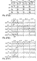
- Figure 2 shows a write operation sequence in a panel in apparatus as illustrated in Figure 1 having a 2-character monitor row (one character in each of display areas 11 and 12) and a 4-character display row capacity (2 rows of two characters, one in each of areas 13 and 14).
- a character "E” is keyed in
- the relevant display area (11) is put into a vertical shift operation mode, being driven from Y-side shift drive circuits 71, 72 and X-side shift drive circuits 75, 76, corresponding to the first display area 11 which has been previously selected by the area selection circuit 60 (in response to signal LGS).
- seven (7) write electrodes W11 1 to W17 corresponding to seven (7) shift channels extending through area 11 are repeatedly selected nine times in succession, in synchronization with shift operation periods, and thereby a character "E" is written into the panel area 11 with a 7 x 9 dot (picture element) configuration, as shown in Figure 2 (1-1) to (1-2). Each time the write electrodes W11 to W17 are selected discharge spots of one seven-dot line making up character "E" are written into the panel.
- Figure 3 illustrates in detail the electrode arrangement of a self-shift PDP, and an example of driving circuitry therefor. It will be appreciated that forms of self-shift PDP other than the self-shift PDP having a meander electrode configuration as shown in the Figure can be employed.
- shift electrodes of two different groups y1 and y2 are arranged in a plurality of vertical lines on one substrate of the panel. Along each line shift electrodes from the two different groups y1 and y2 alternate with one another. Shift electrodes of two further different groups x1 and x2 are arranged in a plurality of vertical lines on the other substrate of the panel, which opposes the one substrate of the panel. Along each line shift electrodes from the two different groups x1 and x2 alternate with one another.
- the respective vertical lines of electrodes on the one substrate of the PDP correspond to respective vertical lines of electrodes on the other substrate of the PDP in such a manner that each electrode in a vertical line on the one substrate overlaps two consecutive electrodes in the corresponding vertical line on the other substrate and such that each electrode in that corresponding vertical line on the other substrate overlaps two consecutive electrodes in the vertical line on the one substrate.
- discharge cells are formed where electrodes on opposite substrates overlap (as viewed in a direction perpendicular to the substrates).
- the electrodes on the two substrates of the panel have dielectric layer coatings, and between the two substrates a discharge space filled with discharge gas is provided.
- Each vertical line of electrodes on the one substrate, together with the corresponding vertical line of overlapping electrodes on the other substrate, provides an individual shift channel.
- a cyclically repeating pattern of discharge cells of four different phases or groups, A to D is provided in accordance with the sequence in which electrodes belonging to the different electrode groups occur along the shift channel.
- a plurality of character display columns are formed by the vertical shift channels.
- each character display column is shown, for simplicity of explanation, each constituted by seven vertical shift channels SC1 to SC7.
- in each shift channel four consecutive discharge cells, one from each of phases A to D are employed for displaying one picture element.
- respective write electrodes are provided, as explained above, overlapping the first shift electrode of group y1 in each shift channel.
- W11 to W17 are provided, and in the second character display column write electrodes W21 to W27 are provided.
- the four shift electrode groups y1, y2 and x1, x2 are connected to the terminals YL1, YL2, YR1, YR2, XL1, XL2, XU1, XU2 by means of busses as shown in the Figure.
- electrodes of group x1 located in display areas 11 and 12 are connected in common to terminal XL1
- electrodes of group x2 located in display areas 11 and 12 are connected in common to terminal XL2
- electrodes of group x1 in display areas 13 and 14 are connected in common to terminal XU1
- electrodes of group x2 in display areas 13 and 14 are connected in common to terminal XU2.
- Electrodes of group y1 located in display areas 11 and 13 are connected in common to terminal YL1, and electrodes of group y2 in display areas 11 and 13 are connected in common to terminal YL2, whereas electrodes of group y1 in display areas 12 and 14 are connected in common to terminal YR1, and electrodes of group y2 in display areas 12 and 14 are connected in common to terminal YR2.
- shift drive circuits 71 to 78 each comprising a pair of transistors Q1 and Q2 (which act as a shift pulser) connected in series between a shift voltage source VS and ground, are connected.
- the write electrodes W11 to W17, W21 to W27 are connected to write drivers 91 to 97, as shown, each of which write drivers comprises a pair of transistors Q3 and Q4 (which act as a write pulser) connected in series between a write voltage source VW and ground. Each write driver is connected in common to two write electrodes, one from each of the two character display columns.
- Figures 4(A) to 4(H) show examples of drive voltage waveforms applied to the panel of Figure 3.
- the waveforms of Figures 4 relate to a case in which the first display area 11 is selected whilst changing operation mode from display mode to shift operation mode, the second and third display areas 12 and 13 are in a half-selected condition, and the fourth display area 14 is in a not-selected condition, as mentioned with reference to Figure 2.
- Figures 4(A), 4(B), 4(C) and 4(D) illustrate electrode voltage waveforms applied to the electrodes of each of the electrode groups x1, x2 and y1, y2 in the selected, half-selected and not-selected display areas respectively.
- the waveforms are applied to the electrodes of the groups concerned, in each display area, via the electrode terminals noted against the waveforms.
- each of the electrode voltage waveforms is made up of four basic pulse trains, labelled (1) to @ in Figures 4, each of unit period duration.
- Figures 4(E), 4(F), 4(G) and 4(H) illustrate cell voltage waveforms which are applied to the discharge cells of each of the four different phases, A to D, in the selected, half-selected and not-selected display areas respectively, as the resultants of the combinations of the voltage waveforms applied to the electrodes making up the cells.
- the cell phase e.g. ai
- Write voltage waveforms, applied to write electrodes for write operations, are omitted from Figures 4.
- the display areas 11 to 14 are all in the display mode (DISPLAY) during period from t0 to t2 shown in Figures 4.
- an overlap pulse OP for controlled firing effect
- shift pulse SP are supplied from the relevant shift drive circuits as indicated in Figures 4, in order to activate discharge cells of phase A (in each of the display areas) and at unit period T1 (t1 to t2), an overlap pulse and a shift pulse are supplied from the relevant shift drive circuits, as indicated in Figures 4, in order to activate the discharge cells of the phase D.
- the discharge cells of phase B and phase C which do not require activation, have applied thereto narrow erase pulses EP as indicated in Figures 4.
- a discharge spot present in a display area is sustained by sway shifting of the spot between two adjacent discharge cells, of phase A and phase D respectively, in accordance with the application of pulses as illustrated. If display mode was to be maintained sway shift operations would be repeated continuously. That is to say, in display mode, waveforms as applied in unit periods To, T1 of Figures 4 are continually repeated over the desired display period and discharge spots in the panel are displayed by being reciprocally shifted between discharge cells of phases A and D.
- FIGs 5(A) to 5(D) illustrate the behaviour of discharge spots in respective shift channels, belonging to display areas 11 to 14 respectively, as caused by the application of waveforms as illustrated in Figure 4 to the panel of Figure 3.
- FIG. 5(A) to 5(D) relating to respective display areas, the behaviour of a discharge spot in a shift channel in the display area concerned through the successive unit periods (steps) TO to T5 of Figures 4 is shown.
- the shift channels are shown horizontally, for ease of understanding, and are schematically indicated by means of electrodes (x1, x2) of the two x-electrode groups formed on one substrate of the panel, and the electrodes (y1, y2) of the two y-electrode groups formed on the other substrate of the panel (and the write electrode W).
- the cells formed between overlapping electrodes are labelled according to the phase to which they belong (e.g. cells a1, a2, a3 belong to phase A, and cells b1, b2, b3 belong to phase B, etc).
- the four basic pulse trains (D to @ are applied to the electrodes of the four electrode groups x1, x2 and y1, y2 in area 11 (from the relevant electrode terminals XL1, XL2 and YL1, YL2) in respective cyclically repeating sequences, so that in each successive unit period the basic pulse trains are applied to the electrodes of the respective different electrode groups in such a manner as to cause progressive forward shifting of a discharge spot.
- each basic pulse train is applied to each electrode group in turn, so that there is a sequential rotation of application of basic pulse trains, from electrode group to electrode group, through the four electrode groups. By repeating such rotation progressive forward shifting is provided.
- FIG. 4(A) One cycle of rotation is illustrated in Figure 4(A), in the four consecutive unit periods T2 (t2 to t3), T3 (t3 to t4), T4 (t4 to t5) and T5 (t5 to t6), in which each basic pulse train is applied for one unit period to each electrode terminal (and hence to each electrode group in area 11).
- a write pulse (not illustrated) can be applied to a selected write electrode in each unit period, corresponding to period T5, in which discharge cells of phase D are activated, and thereby data writing can be effected (a discharge spot written, in period T5, in the write discharge cell W formed by write electrode W and electrode y1, in Figures 5, being thereafter shifted into the shift channel concerned).
- an erase pulse EP is applied to each discharge cell from which the discharge spot has just been shifted, and thereby an erase operation is provided in respect of the discharge spot at that discharge cell.
- the x-electrode groups in each shift channel are connected to the terminals XL1, XL2 in common with the x-electrode groups in the first display area 11, as explained above, and thus the basic pulse trains applied to the x-electrodes in area 12 in successive unit periods are the same as those applied to the x-electrodes in display area 11.
- the y-electrode groups in display area 12 (connected to terminals YR1 and YR2) can receive the basic pulse trains in different sequences (through successive unit periods) from the y-electrode groups in display area 11 (which are connected to terminals YL1 and YL2). Thereby sway shift operations can be provided.
- Figure 4(B) shows the electrode voltage waveforms applied to the different electrode groups in display area 12
- Figure 4(F) shows the resultant cell voltage waveforms applied to discharge cells in shift channels in display area 12.
- step 1 forward shift is effected in the second display area 12 as it is in the first display area so that a discharge spot shifts to a cell of phase A for example, but in the second step, since shift pulses SP are supplied from the terminals YR1 and XL1 (see Figure 4(B)) with respectively inverted phases as compared with the phases in which they are supplied from those terminals in the first step, the discharge spot is maintained at the discharge cell of phase A.
- the basic pulse trains are supplied to the electrode groups in area 12 in the same way as they are during unit period T1 of the display mode as described above, the discharge spot is shifted backwards from the discharge cell phase A to a discharge cell of phase D.
- Figure 5(B) illustrates such shift operations in display area 12, in which a discharge spot shifted in the first step to cell a2 from cell d 1, and thereafter is shifted as follows:- thus executing sway shifting.
- the y-electrode groups in each shift channel are connected to terminals YL1, YL2 in common with the y-electrode groups in the first display area 11, as explained above, and thus the basic pulse trains applied to the y-electrodes in area 13 in successive unit periods are the same as those applied to the y-electrodes in area 11.
- the x-electrode groups in display area 13 (connected to terminals XU1 and XU2) can receive basic pulse trains in different sequences (through successive unit periods) from the x-electrode groups in display area 11 (which are connected to terminals XL1 and XL2). Thereby sway shift operations can be provided.
- FIG. 13 illustrates shifting effected in area 13 over steps 1 to 4, in which a discharge spot is shifted as follows:-
- a discharge spot in a half-selected display area is sustained by reciprocation over a 2- group 2-phase spacial discharge cell arrangement period by means of a sway shift operation.
- shift pulses SP are applied only to one y-electrode group and to one x-electrode group, from terminals YR1 and XU2 respectively, over all the unit periods T2 to T5 and therefore a discharge spot is, for example, maintained in a discharge cell of phase D is a so called stationary display condition.
- Figure 5(D) illustrates such a discharge condition in which a discharge spot is sustained in discharge cell d 1.
- display information (data characters) in a half-selected display area is sustained by a sway shift operation so that each discharge spot stays within a specified spatial discharge cell arrangement, through which it reciprocates periodically, whilst ordinary forward shift operation is being effected in a selected display area, and simultaneously information (data characters) in a not-selected display area is sustained in a stationary display condition within a specified spatial cell arrangement.
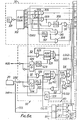
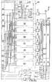
- Figures 6a to 6c make up a block diagram illustrating particularly driving circuitry for use in apparatus embodying this aspect of the present invention for realizing selective data write/shift operations in each display area of the above- described self shift PDP 10 and for realizing sustaining operations therein.
- basic timing signal generator circuit 30 which controls the generation timing of the four basic pulse trains 1, 2, 0) and @ mentioned above, has as its main component a binary 6-bit counter 302 which counts up clock pulses sent from a clock pulse generator 301 and supplies 6-bit outputs b1 to b6.
- the first and second bit outputs b1 and b2 are inverted in inverters 303 and 304 respectively and then delivered to respective inputs of AND gate 305 which outputs a 1 st timing signal corresponding to the abovementioned basic pulse train 1, including shift pulse SP, to a conductor line (1) over every count of four clock pulses.
- the inverted first bit output b1 and the second bit output b2 are supplied to AND gate 306 which outputs a 2nd timing signal corresponding to the abovementioned basic pulse train @, including shift pulse SP, to a conductor line (2).
- the inverted first bit output b is supplied to a monostable circuit 307, to provide for generation of erase pulses EP, and the inverted second bit output b2 is supplied to one input of AND gate 308, to another input of which the output of circuit 307 is supplied, and thereby a 3rd timing signal corresponding to the abovementioned pulse train h is output to a conductor line (3) from the output of AND gate 308.
- the logical AND product of the inverted third bit output b3 and the output of the AND gate 306 is supplied to monostable circuit 309, to provide for generation of overlap pulses OP.
- the output of the monostable circuit 309 is supplied to one input of OR-gate 311.
- the output of monostable circuit 307 (providing for erase pulses) is applied to one input of AND gate 310, to respective further inputs of which the second and third bit outputs b2 and b3 are supplied.
- the output of AND gate 310 is supplied to a second input of OR gate 311.
- the output of the OR gate 311 delivers pulses from monostable 309 (for overlap pulses) and (when bit outputs b2 and b3 open AND gate 310) pulses from monostable 307 (for erase pulses).
- the output of OR gate 311 provides a 4th timing signal corresponding to the abovementioned basic pulse train @, which is output along conductor line (4).
- this generator circuit 30 outputs a signal indicating the number of times that shift operation is carried out, as explained in more detail below.
- the discharge cells are divided between 4-groups and 4-phases in a cyclically periodic arrangement, four unit periods form a shift operation cycle and, in relation to the circuitry of Figure 6, one unit period corresponds to the time over which 16 successive clock pulses are counted.
- the 6th bit output of counter 302 indicates the counting of 64 successive clock pulses by the 6-bit counter 302 and thus corresponds to signal (SNS) (shift operation number signal) which indicates the end of one shift operation cycle.
- the control signal generator circuit 50 comprises an ordinary write/shift control command circuit 51, a roll-up control command circuit 52, an area selection command circuit 53, and an operation change-over control circuit 54.
- the ordinary write/shift control circuit 51 issues a command to cause writing of data characters, corresponding to character data keyed in from the keyboard (20 in Figure 1), into the lower display areas (monitor rows) 11 and 12.
- the roll-up control command circuit 52 issues a command to cause roll up of data characters displayed in the display areas 11 and 12 into the upper display areas (display rows) 13 and 14. These two command circuits are very similar.
- the character pattern (fount) is made up of 7 x 9 dot patterns as described previously, and a 7- dot inter-character spacing is provided.
- Each character is made up of a 7 x 9 pattern of dots, or picture elements, thus, considering a rectangular 7 x 9 array of dots or picture elements, by causing discharge spots at some dot locations in the rectangle, and not at others, the appearance of a data character can be given by the discharge spots.
- each character is built up of nine horizontal lines, each of seven dots, vertically above one another. Between characters which are displayed vertically one above another a spacing corresponding to seven picture element heights (i.e. seven successive horizontal lines of picture elements) is provided.
- the circuits 51 and 52 are so configurated that after sixteen shift operation cycles (corresponding to the writing of nine lines, each of seven dots (to make up a character), in respective successive shift operation cycles, and a character spacing of seven lines (taking a further seven shift operation cycles), a new character writing timing signal appears (in response to which a further character can be written).
- the circuits 51 and 52 have as their main components 4-bit counters 51 and 521 which are reset to an initial condition after every sixteen shift operation number signals SNS are counted in those counters, NAND gates 512 and 522 which each have four inputs that are connected to respective outputs of the four-bit counter associated with the NAND gate (counter 521 is associated with NAND gate 522, and counter 511 is associated with NAND gate 512), and which each output (after the associated counter has been reset) a shift operation command output "1" until the associated counter is counted up to sixteen (all outputs 1) indicating that sixteen SNS signals have been received since the last reset, monostable circuits 513 and 523 which output reset signals for resetting the counters to their initial conditions after a sixteen count has been reached, flip-flip circuits 514 and 524 which control monostable circuits 513, 523 in response to the abovementioned write command signal STB and roll up command signal RUS which are delivered selectively thereto, and AND gates 515 and 525 which supply said signals
- the 4-bit counters 51 and 521 count SNS signals from the 6th bit output of 6-bit counter 302.
- a 4-bit counter 51 or 521 counts up to sixteen and its outputs all become “1” the application of counting inputs (SNS) signals to the counter is blocked at AND gate 515 or 525, respectively, when the output of NAND gate 512 or 522, respectively, becomes "0".
- the counter 511 or 521 is reset by means of an output from monostable circuit 513 or 523, respectively, controlled by outputs of flip-flops 514 and 524 respectively.
- the flip-flops 514 and 524 receive the SNS signals and, respectively, write command signal STB and roll-up command signal RUS.
- the flip-flops 514 and 524 are operated to cause the monostable circuits 513 and 523, respectively, to generate an output to reset counters 511 and 521 respectively, in response to command signals STB and RUS indicating a new character writing or roll-up period is to begin.
- the outputs of NAND gates 512 and 513 are employed, via an inverting OR gate, to provide next character write command MR.
- the area selection command circuit 53 issues commands for selecting ordinary write/shift operations for the first display area 11 and for the second display area 12.
- areas 11 and 12 are selected alternately when write command signals STB are input.
- the circuit 53 comprises a flip-flop 531 which switches between its two output conditions in response to the input of command signals STB.
- the operation change-over control circuit 54 controls change-over between ordinary shift operations and roll up operations for the display areas selected in response to the command signal sent from said command circuit 53.
- the circuit 54 comprises a pair of AND gates 541 and 542 which are opened alternately, with alternation of the output conditions of flip-flop 531, and which pass the output of NAND gate 512 (the ordinary shift operation command output) to OR-gate 544 or to OR-gate 543 in dependence upon which of AND gates 541 and 542 is opened.
- AND gate 541 generates logic output "1" (when it is opened)
- the first display area 11 is selected for ordinary shift operation
- AND gate 542 generates logic output "1" (when it is opened) the second display area 12 is selected for ordinary shift operation.
- the OR gates 543 and 544 both receive the output of NAND gate 522, and thus in the circuitry of Figure 6 roll up operations for the left-hand display area and the right display area are performed together, simultaneously.
- the timing selection circuit 40 has two circuit blocks 41-1, 41-2, each of which comprises four pairs of AND gates 411-412; 413--414; 415--416; and 417 ⁇ 418: and OR gates 421, 422, 423, and 424 each of which has two inputs connected to the outputs of respective AND gates of a respective pair.
- One input of one AND gate of each AND gate pair (one input of each of AND gates 411, 413, 415 and 417) as connected to receive the 5th bit output of the abovementioned 6-bit counter 302 in inverted form, whilst one input of the other AND gate of each AND gate pair (one input of each of AND gates 412, 414, 416 and 418 receives the 5th bit output of said counter 302 in uninverted form.
- Each of the other inputs of the AND gates of the pairs is connected to a conductor line (1), (2), (3), (4) to receive basic pulse trains (D to @, in the pattern shown in Figures 6.
- the circuit blocks 41-1 and 41-2 each output respectively, along output conductor lines (A) to (D), and (I) to (L), respectively, different selections of basic pulse trains and switching between those selections takes place in dependence upon the 5th bit output of counter 302. That is to say the two different selections are output in alternate unit periods.
- the selection circuit 40 also comprises four circuit blocks 42-1, 42-2, 42-3, and 42-4, as is clearly shown in Figures 6, each comprising four pairs of AND gates 431 to 434 each of which is composed of four gates, an OR gate 451 and a 4-line decoder 461 which is connected to decode the fifth and sixth bit outputs of 6-bit counter 302.
- circuit blocks 42-1 to 42-4 are provided for outputting the basic pulse trains one by one along output conductor lines (E) to (H) respectively in respective predetermined sequences in dependence upon the conditions of the fifth and sixth bit outputs of counter 302.
- the area selection circuit 60 in the circuitry of Figures 6, is the circuit which selects between the four display areas 11 to 14 of the panel 10.
- This circuit 60 comprises eight circuit blocks 61 to 68 which are inserted between the output conductor lines (A) to (L) of the timing selection circuit 40 and the eight shift drive circuits 71 to 78 mentioned previously.
- the circuit blocks 61 to 68 all have the same circuit configuration excepting that they are connected to different combinations of the output conductor lines (A) to (L) at their inputs.
- each of circuits 61 to 68 comprises four pairs of AND gates 611 to 614 each of which is composed of four gates, an OR gate 615 and a 4-line decoder 616 for decoding logic signals LGS1, LGS2 delivered from said control signal generator circuit 50.
- AND gates 611 to 614 respective output lines of the 4-line decoder 616 are connected, whilst to the other inputs of each of the AND gates 611 to 614, output conductor lines are respectively connected in the combinations as shown in the Figure.
- OR gate 615 has four inputs connected respectively to the outputs of respective AND gates 611 to 614, and the output of the OR gate is connected to a shift drive circuit 71 to 78.
- the write signal generator circuit 80 comprises a character generator 81 which outputs a sequence of character pattern signals IF1 to IF7, for building up character patterns of 7 x 9 dots, 7 dots at a time (7 dots, making up one line of a character in every four unit periods).
- the sequence of character pattern signals, and hence the character pattern is selected in dependence upon character code signal CCS (delivered from keyboard 20).
- the signals IF1 to IF7 are passed to respective NAND gates 821 to 827, which also receive basic pulse train @, to ensure synchronization of the signals with write timing.
- Write driver circuit 90 comprises write drivers 91 to 97, inputs of which are connected to the outputs of respective NAND gates 821 to 827, and the outputs of which are connected to write electrodes in the panel 10 in the manner described previously.
- Figure 7 is a tabular diagram illustrating sequences of basic pulse trains to be applied to the electrode terminals supplying electrodes in the different display areas (11 to 14) in the panel 10 for respective single cycles of respective operation modes, i.e. display mode, forward shift and roll up.
- the logic signals LGS1, LGS2 output from said control signal generator circuit 50 are all "0" and therefore the decoders 616 in each of the circuit blocks 61 to 68 of the area selection circuit 60 each give a first bit output with a logic level "1".
- AND gates 611 in the respective circuit blocks 61 to 68 are opened to allow four basic pulse trains sent from the circuit blocks of said timing selection circuit 40 to pass in parallel in each step in such a manner that they are applied to the terminals YL1, YL2, YR1, YR2, XL1, XL2, XU1, XU2, in successive steps in the four steps of a display operation cycle, in the sequences shown in Figure 7 for the DISPLAY mode.
- the basic pulse trains passed by the AND gates 611 1 are sent to the corresponding OR gates 615 in the respective circuit blocks 61 to 68 and are then supplied in parallel to the shift drive circuits 71 to 78.
- discharge spots are sustained by sway shifting between two discharge cells, of phase D and phase A, respectively, in accordance with the sequence of the basic pulse trains applied in each operation step.
- LGS1 takes a "1" level
- LGS2 takes a "0” level in response to the output from the flip-flop 531 when a write command signal STB is issued when data is keyed in from keyboard 20.
- the second bit outputs of decoders 616 in circuit blocks 61 to 68 become “1".
- AND gates 612 are opened to pass in parallel in each step basic pulse trains output from circuit blocks 41-1, 41-2, and 42-1 to 42-4 of the timing selection circuit 40 in the sequences shown in Figure 7 for FIRST AREA (FORWARD SHIFT).
- each write driver in the write driver circuit 90 is connected in common to write electrodes in the same pos - ition in each of the first and second display areas, but in respect of the half-selected area (area 12 in the present example) in which sway shifting is effected, write discharges are generated at the timing of activation of cells of phase D as they are in respect of area 11 in which forward shifting is effected, but in area 12 such written in discharges disappear in the course of the backward shift part of sway shifting and thereby such written in discharges are invalidated so that writing is validly effected only in area 11.
- the output condition of the flip-flip 531 is changed in response to a write command signal STB which is generated by data keying at keyboard 20 and thereby the logic signal LGS1 becomes “0", while logic signal LGS2 becomes “1".
- the 3rd bit outputs of the decoders 616 in the circuit blocks 61 to 68 become “1" and corresponding AND gates 613 are thereby opened.
- both the logic signal LGS1 and LGS2 become “1" in response to a roll up command signal RUS which is generated by an operator's command and thereby the 4th bit outputs of the decoders 616 in the circuit blocks 61 to 68 become “1".
- corresponding AND gates 614 are opened and as a result the basic pulse trains sent from the corresponding circuit blocks 42-1 to 42-4 of the timing selection circuit 40 are delivered to the shift drive circuits 71 to 78 via the AND gates 614 and the OR gates 615.
- the basic pulse trains are delivered to the shift drive circuits in the sequences as shown in Figure 7 in ROLL UP.
- all of the display areas 11 to 14 are set in a forward shift operation mode, and data in the first and second display areas 11 and 12 is shifted up into the upper, third and fourth display areas 13 and 14, and is thereby rolled up.
- gas discharge display apparatus embodying the first aspect of the present invention including a setf shift PDP and driving circuitry therefor, display functions can be enhanced by the employment of partially selective shift operations as described above.
- the display screen provided by the self shift PDP has, for the sake of simplicity and clarity, been considered as being divided into four display areas only.
- the panel is divided parallel to and perpendicular to the shift channels of the panel.
- the display screen may be divided into more than four areas.
- a first data character is written into a first display area (by driving write drive circuits which supply electrodes which make up write discharge cells through which discharge spots are written into the first display area), and when the first data character has been written, a second data character is then written into a second display area, and so on, complete character by complete character.
- This problem may be more acute when the apparatus operates such that characters already being display in each of the lower display areas (that is the areas into which data characters are initially written in the arrangements described above with reference to the Figures) are rolled up into corresponding upper display areas simultaneously with the writing of a next data character into the lower display area concerned.
- a self-shift PDP in apparatus embodying the second apparatus aspect of the present invention in which there are provided a plurality of parallel shift channels, the panel is divided as in the apparatus of Figure 1, between different display areas, in parallel with the shift channels, and the driving circuitry of the apparatus is such that when writing data characters into each of a plurality of display areas, the characters are written into all those display areas substantially simultaneously.
- data specifying data characters to be written is input in units of picture element (dots) by alternately selecting a pair of display area in the vertical direction of plural pairs and corresponding write discharge cell.
- each data character as having a 7 x 9 picture element structure, that is each character comprising nine horizontal lines of seven picture elements each, one line above another
- first one line of seven picture elements relating to the character to be written in area 11 is written into area 11, then one line of seven picture elements is written into area 12, then a next line of picture elements is written into area 11, and so on, until the characters in areas 11 and 12 are both complete.
- the characters seem to appear substantially simultaneous in areas 11 and 12.
- shift or roll up operations can be performed for the left-hand and right-hand display areas alternately, so that characters therein are shifted or rolled up picture element line by picture element line alternately.
- FIG 8 is a schematic block diagram of apparatus embodying this second aspect of this invention wherein display area selection and data character writing can be effected as explained above.
- the self-shift PDP is divided into four display areas, parallel to and perpendicular to the shift channels thereof.
- the roll up command signal RUS of the control signal generator circuit 50 is so changed that the left and right-hand sides of the display screen can be set into a selective shift operation mode alternately, so that picture element lines are written into the two sides of the screen alternately.
- the distribution sequence of the four basic pulse trains of the area selection circuit 60 is so changed that operations, particularly roll up operations, can alternately and selectively performed so that data characters in the left and right-hand sides of the display screen can be rolled-up, picture element by picture element, with roll up on one side of the screen alternating with roll up on the other side of the screen.
- the write signal generator circuit 80 is so changed that character pattern signals IF1 to IF7 are generated in dependence upon pattern generation selection signals PGS as well as in dependence upon a particular basic pulse train (the timing of pulse train @).
- the pattern generation selection signals PGS correspond to the shift operation number signal SNS for ordinary write operations, and to two such shift operation number signals during a roll up operation period.
- display area memory circuit 100 in the case of the apparatus shown in Figure 8, comprises two display area memories 100A, 100B which correspond respectively to the left and right-hand parts of the display screen, and it reads the single character data keyed in simultaneously with writing the code signal CCS1 of said character in response to said write command signal STB, while it once stores the code signal CCS2 for the character data of plural rows structures sent from the not illustrated computer terminal and sequentially reads said data in replay to said roll up command signal RUS.
- the display area memory circuit is operable to read keyed-in single character data, simultaneously writing the code signal CCS1 designating the character in response to the write command signal STB.
- the circuit also stores code signal CCS2, sent from a computer terminal (not shown), for designating a format or structure (for example a table format) for display of characters in a plurality of rows.
- the circuit is operable to sequentially read out stored data in response to roll up command signals RUS.
- Memory 100 also stores a display screen selection signal MSS, which will be explained later, and thereby any desired one of the two display memories 1 OOA, 1 OOB can be caused to function selectively.
- row selection control circuit 110 selects left-hand or right-hand display area memory 100A or 100B, corresponding to the left-hand or right-hand display screen, for data writing, and also selects a display row of the selected display area memory.
- the circuit 110 selectively receives the write command signal STB and the roll up command signal RUS and generates a display screen selection signal (for selecting between the left-hand and right-hand parts of the display screen) MSS and a row selection signal RSS.
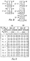
- Figure 9 illustrates a write operation sequence in the panel 10, of the apparatus of Figure 8, having a 2-character monitor row and a 4-character display row capacity.
- a code signal CCS1 corresponding to that character is written into the previously selected left-hand display area memory 100A and simultaneously is read out therefrom.
- the readout character code signal CCS is input to the write signal generator 80 and converted therein into the character pattern signals IF1 to IF7, which are then supplied to write drive circuit 90.
- the relevant area is set into a vertical shift operation mode by the Y-electrode shift drive circuits 71, 72 and the X-electrode shift drive circuits 75, 76 corresponding to that first display area 11 which has already been selected by operations of the area selection circuit 60.
- the second display area 12 and the third display area 13 are in a half-selected condition and thereby previously displayed characters "F” and "S” are sustained therein by means of sway shift operations, as shown in Figure 9 (1-1) and (1-2).
- the fourth display area 14 is in a not-selected condition and thereby previously displayed character "L” is sustained therein in a stationary display mode as shown in Figure 9 (1-1) and (1-2).
- each character in the left-hand display areas are first shifted upwards by one picture element spacing, that is each discharge spot is shifted up into the position previously occupied by the discharge spot above it in the character concerned, then the characters in the right-hand display area are shifted upwards by one picture element spacing, and on on).
- the characters in the left-hand and right-hand display areas are shifted upwards alternately, picture element line by picture element line.
- each character comprises nine lines, each of seven picture elements, and in the apparatus of Figure 8 the characters are shifted upward line by line, alternating line by line between characters in the left-hand display areas and characters in the right-hand display area.
- Such operations are effected as explained below by issuing a roll up command.
- the left-hand and right-hand display areas 11, 13 and 12, 14 are alternately set into a vertical shift operation mode, picture element by picture element (line by line), in response to the roll up command signal RUS and the left-hand and right-hand display area memories 100A, 100B are alternately placed in a read out operation mode, picture element by picture element (line by line), for reading out character data relating to data characters to be displayed in a desired display row, by means of display area selection signal MSS and row selection signal RSS sent from row selection control circuit 110.
- stored character data relating to a first display row, from the two display area memories 100A, 100B, is employed to write characters into the corresponding first and second display areas 11, 12 in such a manner that the write driver circuits used in common for writing into the first and second display areas 11, 12 are driven alternately by character data from the memories 100A and 100B, so that characters to be displayed in the area 11, 12 are written in alternately, picture element by picture element (so that one character line of seven dots is written into the first display area, then one character line is written into the second display area, and so on).
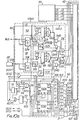
- Figures 10a and 10b make up a block diagram illustrating in detail particularly driving circuitry for use in apparatus conforming to the configuration shown in Figure 8.
- Control signal generator circuit 50 of Figures 10 differs from the circuit 50 of Figures 6 only in relation to roll up control command circuit 52 and operation selection control circuit 54. Thus, a description relating to these latter circuits will be given.
- flip-flop circuit 525 is newly added as compared with Figures 6, and the inputs applied to one input terminal of AND gate 526 (corresponding to AND gate 525 in Figure 6) and to clock terminals of the flip-flop circuit 524 (corresponding to flip-flop 524 in Figure 6) are modified as compared with Figures 6.
- the flip-flop 525 enables shift operations to take place for the first and second display areas alternately, picture element line by picture element line, during roll-up operation. Moreover, flip-flop 525 receives at an input thereof the shift operation number signal SNS (from line 15 in Figures 10) and the logical level "1" appears at each of its two output terminals alternately.
- AND gate 526 in Figure 10 receives at one input the output SNS1 from one output terminal of flip-flop circuit 525 and delivers it to the 4-bit counter 521. Thus, since SNS1 has logic level "1" for every other shift operation, logical level "1" is delivered to 4-bit counter 521 for every other shift operation (of one picture element line).
- NAND gate 522 generates a shift operation command output "1" over the whole of a period during which 32 shift operation number signals SNS are output from basic timing signal generator circuit 30. Also, the signals SNS1 are applied to the clock terminal of flip-flop 524, an output of which controls monostable 523 and constitutes LGS3.
- a pair of AND gates 545 and 546 for providing a command output to cause shift operations for roll up, is newly added as compared with Figures 6.
- One input of each of AND gates 545 and 546 is connected to the output terminal of NAND gate 522, while the other inputs of the AND gates 545 and 546 are connected to respective output terminals of flip-flop 525.
- the area selection circuit 60 of Figures 10 is modified significantly as compared with Figures 6, as explained below in more detail.
- circuit blocks 61 to 68 each comprise of five pairs of AND gates 611 to 615 each of which is composed of five gates, an OR gate 616 and a 7-line decoder 617 for decoding three logic signals LGS1 to LGS3 supplied thereto from control signal generator circuit 50.
- the 1 st, 2nd, 3rd, 6th and 7th line outputs of the decoder 617 are connected to inputs of respective different ones of the five AND gates of the circuit block, AND gates 611 to 615.
- Each AND gate 611 to 615 has connected to its other input an output conductor line of circuit 40.
- the connection arrangement being as shown in Figure 10.
- the output of OR gate 616 which receives the outputs of the AND gates 611 to 615 is connected to a shift drive circuit 71 to 78.
- Display area memory circuit 100 comprises a first display area memory 100A and a second display area memory 100B which respectively correspond to left and right screens divided vertically.
- These memories 100A, 1008 are not limited to the particular configuration illustrated, but are taken, for simplicity, to have in this case a 4 row memory capacity, and are therefore provided each with 2-bit address terminals AO and A1. These memories are also provided each with a display screen selection terminal Cs and a write/read terminal W/R, and thereby a desired display area memory can be subject to selective write and read operations in dependence upon the display screen selection signal MSS which will be described later, and the outputs of write command circuit 51 and monostable circuits 513 and 523 or roll up command circuit 52. These memories are furthermore provided with data input terminals Di1 to Di6 for receiving character code signals CCS1 and CCS2 of a 6-bit configuration sent from keyboard 20 and a computer (not illustrated), and 6-bit data output terminals D01 to D06.
- Row selection control circuit 110 is provided for automatically performing line feed and selection between display area memories (100A, 100B) when writing a single character and when writing characters to be displayed in different display rows, character data relating to which has been previously stored in display area memory circuit 100 by means of keyboard 20.
- the circuit 110 includes a binary counter 111; a 4-step counter 112; AND gates 113, 114; OR gates 115 and 116; and inverter 117.
- the binary counter 111 is used for counting the number of input characters, which it counts in response to the falling edges of output pulses from NAND gate 512 of write command circuit 51.
- the 4-step counter 112 is provided for counting the number of rows on which characters are to be displayed. This counter is connected to receive the output of binary counter 111 via OR gate 115 and to receive the output of NAND gate 522 of said roll up command circuit 52 via OR gate 115, and selectively counts those outputs. A count of those outputs is used as row selection signal RSS.
- the pair of AND gates 113 and 144, and OR gate 116, are provided for controlling the display area memories 100A, 100B.
- AND gate 113 is connected to receive at respective inputs thereof outputs of NAND gate 522 and flip-flop 525 of the roll-up command circuit 52 and generates an output of logical level "1" when a roll-up command is issued.
- AND gate 114 is connected to receive at respective inputs thereof outputs of NAND gate 522 (received via inverter 117) and binary counter 111, and generates an output of logical level "1" when an ordinary write command is issued.
- OR gate 116 which receives the outputs of AND gates 113 and 114, outputs display screen selection signal MSS which can take either of logical levels "1" and "0" in dependence upon the logical levels of the outputs of the AND gates. For example, when MSS is "0", the left-hand display area memory 100A is selected, and when MSS is "1 ", the right-hand display area memory 100B is selected.
- pattern generation selection circuit 83 is newly added as compared with Figures 6. This circuit 83 is provided for controlling write operations, so that writing can take place picture element line by picture element line, when the ordinary write command and roll up command are issued, and has the following configuration.
- the circuit 83 includes a first group of AND gates 832, 834, 836, 838 which gates are opened to pass the outputs (e, f, g, h) of counter 521, when a roll up command is issued, in response to the output of the NAND gate 522 of roll up command circuit 52 having logical level "1", a second group of AND gates 831, 833, 835, 837 which are opened to pass the outputs (a, b, c, d) of counter 511 of write command circuit 51 when no roll up command is issued, that is when no ordinary write command is issued, and a group of OR gates 839 to 842 each of which is connected to receive the outputs of two AND gates, one from each of the first and second groups.
- the outputs of the OR gates are input to character generator 81 as pattern generation selection signals PGS, and thereby the generator can generate the selected character pattern signals IF1 to IF7, for developing characters of a 7 x 9 dot form.
- Figure 11 is a tabular diagram, of a form similar to that of Figure 7, illustrating sequences of basic pulse trains applied to electrode terminals supplying electrodes in the different display areas of the self-shift PDP of the apparatus of Figure 10 for respective single cycles (four unit period steps) of respective operation modes ROLL UP (LEFT SCREEN) and ROLL UP (RIGHT SCREEN).
- Figure 11 relates to a case in which character data relating to two display rows, stored previously in the display area memory circuit 100, is to be used to generate data characters in the self shift PDP. Circuitry operation in the apparatus of Figures 10 will be explained with reference to Figure 11.
- flip-flop 524 When an operator issues a roll up command, flip-flop 524 operates in response to the roll up command signal RUS and generates an output signal of logical level "1". This signal drives monostable circuit 523, resetting the outputs of counter 521, and is also applied to area selection circuit 60 as logical signal LGS3. At this time, the flip-flop 525 receives shift operation number signal SNS and outputs a "0" signal from its Q output terminal and a "1" " signal from its Q output terminal. When counter 521 is reset, NAND gate 522 outputs a "1” signal, and therefore the output "1" of the output terminal of flip-flop 525 is passed through AND gate 546 and enters OR gate 543. Thus, the logical signals LGS1, LGS2 generated from the OR gates 543, 544 becomes “1", "0” respectively.
- character generator 81 output signals IF1 to IF7 designating the character pattern only of a first line of nine lines which are selected by the character code signal CCS and which together make up the designated character (That is to say, a 9 x 7 dot form character is made up of nine lines each of seven dots, and initially character generator 81 outputs signals IF1 to IF7 relating only to the first line of seven dots).
- the output pattern signals relating to the first character line are passed through NAND gates 821 to 827 in synchronization with the generation timing of basic pulse train @ and are supplied to the corresponding write drive circuits 91 to 97. Thereby these write drive circuits apply write pulses PW to selected write electrodes as mentioned previously and generates discharge spots at the selected write discharge cells in areas 11 and 12.
- the discharge spots generated at the selected write discharge cells in area 11 are then shifted through a sequence of discharge cells of phases A - B ⁇ C in accordance with the vertical shift operation mode effective for the first display area 11, but in area 12 the discharge spots generated are sway-shifted through a sequence of discharge cells of phases A ⁇ A ⁇ D (write cell W) in accordance with the half-selected operation mode effective for the second display area 12 and thereby disappear. Therefore, only in the first display area 11 is the stored character data read out from the left-hand display area memory 100A effective to write in one line of dots going to make up a character. (That line of dots corresponds to a picture element.)
- the second and fourth display areas 12, 14 on the right-hand side are put in a vertical shift operation mode and the first and third display areas 11, 13 on the left-hand side are put in a half-selected operation mode.
- the display screen selection signal MSS becomes "1 ", designating the right display area memory 100B for operation.
- row selection signal RSS continues to designate a first display row as in the case described above. Therefore, stored character data relating to a first display row on the right-hand display area 12 is read out from display area memory 1 OOB and input to character generator 81.
- the pattern generation selection signals PGS designate the first line also, as in the case given above, character pattern signals IF1 to IF7 relating to a first line of a character to be displayed in the first row are supplied to the write drive circuits 91 to 97 as in the case described above.
- discharge spots are generated at selected write discharge cells relating to a first line of a character.
- Discharge spots generated in second display area 12 are sequentially shifted through a sequence of discharge cells of phases A ⁇ B ⁇ C in accordance with the vertical shift operation mode effective in the second display area 12, but discharge spots generated in the first display area 11 are caused to disappear in the manner described above, by the sway shift operation mode effective in the first display area.
- a discharge spot which has been previously written into the first display area 11 and which is present in a discharge cell of phase A spaced by one picture element spacing from the write cells is sway-shifted through a sequence of discharge cells of phases and is thereby sustained by reciprocating between that discharge cell of phase A and the first discharge cell of phase D (nearest the write discharge cells).
- stored data read out from the right-hand display area memory 100B is employed for writing one line of discharge spots (a picture element) going to make up a data character in second display area 12.
- shift operation number signal SNS is generated again, inverting the output condition of flip-flop 525.
- the left-hand display area memory 100A is selected and the left-hand display areas 11, 13 are put into the write/shift operation mode.
- the counter 521 performs a counting operation in response to the falling edge of the Q output of flip-flop 525 and the 1 st bit output thereof takes a logical level "I".
- the logical value of the pattern generation selection signals PGS becomes "0001", designating character patterns relating to a second line of the first display row. Therefore, write operations for writing discharge spots in accordance with the character pattern signals relating to that second line are carried out. Thereby the operations relating to the writing of the first line of the first display row in the left-hand display areas 11, 13 are repeated in respect of the second line, then the second line of the first display row in the right-hand display areas 12, 14 is written, and so on until writing for the first display rows in the left-hand and right-hand display areas is complete.
- line feed is performed automatically by means of the following operations and thereafter stored data relating to second display rows can be employed for writing.
- characters of the first display rows which are already being displayed in the lower, first and second display areas 11, 12 are rolled up alternately, picture element line by picture element line, by means of the vertical shift operation mode effective in the upper, third and fourth, display areas 13, 14 which vertical shift operations are carried out in those areas alternately and repeatedly for each successive picture element line.
- characters of a second display row are being written into the lower display areas
- characters of the first display row, already being displayed are rolled up into the upper display areas.
- operation margins can be increased by employing in the apparatus a method embodying this invention such that whilst data characters are being written into a selected display area (section of the display screen) and are being shifted into that area, data display in a half-selected display area is sustained by a sway shift operation and, simultaneously, in a not-selected display area, data display is sustained in a stationary display mode.
- a double cell activation driving method can be employed, to obtain high display intensity, wherein adjacent discharge cells are activated in pairs, instead of the single cell activation method employed in the embodiments of this invention described above.
- Figures 12(A) to 12(H) illustrate driving voltage waveforms which can be used, with apparatus comprising a self-shift PDP as shown in Figure 3, to put such a double cell activation method into effect.
- the waveforms of Figures 12 they are those which are applied when the first display area 11 is selected, the second and third display areas 12, 13 are half-selected and the fourth display area 14 is not-selected, respectively.
- write pulses WP are applied simultaneously to the write electrodes W11 to W17 (relating to first display area 11) and W21 to W27 (relating to second display area 12), write voltage waveforms Was shown in Figures 12(E) and 12(F) are applied to write discharges cell W relating to the first and second display areas respectively.
- each discharge spot generated at a discharge cell a1 is shifted to a pair of adjacent discharge cells a1, b1 of phases A and B in accordance with the switching over of the application of the basic pulse trains which takes place.
- these discharge spots in the case of the selected first display area 11, are shifted sequentially in the following unit periods T2, T3 along the relevant shift channels SC1j in such a manner that they are held in successive pairs of adjacent discharge cells (e.g. b1, c1 and c1, d1 and so on) in accordance with sequences of application of the basic pulse trains as shown in Figures 12.
- erase pulses EP are effectively applied to discharge cells from which a discharge spot has just been shifted, as a result of a small phase difference ze provided between pulses applied to overlapping electrodes forming discharge cells, and thereby erase operation in respect of the just shifted discharge spot is performed at the distance cell just left.
- Figure 13(A) illustrates shift operation in the selected first display area 11 in a manner similar to the illustration given in Figures 5.
- write discharge spots generated in area 12 together with write discharge spots generated in the selected area 11 in course of write operations are at the timing of unit period T3 erased when an erase pulse EP is applied to discharge cell a1 as shown in Figure 13(B).
- discharge spots are truly written into selected area 11 only.
- discharge spots are present, at the beginning of unit period T0, in discharge cells d1 and a2 in shift channels of the half-selected area 12, those discharge spots are sustained by a reciprocating or sway shifting movement between adjacent pairs of adjacent discharge cells, through the sequence of discharge cells by the application of pulse trains in sequences in accordance with the abovementioned sway shift operation mode.
- a sway shift operation as shown in Figure 13(D) is carried out by means of driving voltages as shown in Figures 12(D) and 12(H).
- the double cell activation system can ensure high display intensity in each display area and can provide for increased operation margin in a display area which is in a not-selected condition.
- any of various kinds of self shift PDPs for example, having a crossing electrode configuration, a parallel electrode configuration or a meander channel configuration, can be employed in place of a self-shift PDP having a meander electrode configuration as described above.
- a selective partial erasing method embodying this invention, can be employed, wherein erasing operations can be effected in respect of each display area individually in order to prevent the overlap of display data at the boundaries between upper display areas and lower display areas.
- the area 11 when writing new data into the first display area 11 when data has already been written into and is being displayed in the display areas 11, 13, the area 11 must be set into the shift operation mode in order to bring the discharge spots relating to the new data into the appropriate positions in area 11 and, therefore, discharge spots corresponding to the previously written display data in area 11 are also shifted in the forward direction (vertically, to area 13) as explained above.
- the discharge spots of the previously written display data are shifted into the third display area 13 as discharge spots relating to new data are shifted into area 11.
- those discharge spots relating to previously written data, which are shifted towards area 13 from area 11 may come to overlap with discharge spots corresponding to the previously displayed data in area 13.
- Such overlap occurs only at the common boundary of the display areas 11 and 13 since the third display area 13 is in a sway shift operation mode, but as a result of the overlap, a faulty data display may be induced.
- a shift (sustain) pulse used for conditioning discharge cells for erasure, is applied to the electrodes of one y- (or x-) electrode group in the display area selected for erasing data and thereafter a narrow erase pulse is applied to the electrodes of the other x- (or y-) electrode groups.
- a narrow erase pulse is applied to the electrodes of the other x- (or y-) electrode groups.
- Figures 14 shows driving voltage waveforms which can be employed to enable such selective partial erasing operations, in relation to a case in which the first display area 11 is selected (switched) to erasing operation mode from a display mode.
- driving voltage waveforms the same as the voltage waveforms in step 1 of Figure 11 are applied to the electrode terminals supplying the display areas in the period t11 1 to t12, and therefore all display areas 11 to 14 display data in a condition such that discharge cells of phase D and phase A are activated in all areas.
- the erase pulses EP applied to the X-electrode terminals XL1, XL2 of the first display area are also manifest in the second display area, but since in relation to the second display area each erase pulse is of the same polarity as that of an immediately proceeding shift pulse applied to a discharge cell (of phase A or D), as is clear from the cell voltage waveforms shown in Figure 14(D), such erase pulses do not have any effect on the activated discharge cells in the relevant display area 12 and resultingly discharge spots in those cells are sustained.
- the selective partial erasing system is operable to erase displayed data only from the selected first display area 11 and displayed data can be sustained in the other, second to fourth display areas 12 to 14. Therefore, problems of overlap of data at the boundaries between vertically adjacent display areas can be prevented.
- erase pulse timing can be set as desired after generation of the shift pulse.
- apparatus embodying aspects of this invention a self shift type gas discharge panel and driving circuitry therefor are employed which can significantly enhance display functions and improve operationability.
- apparatus embodying aspects of this invention may be of great utility when adopted in the field of monitor display for terminals of computer systems.
- gas discharge display apparatus comprising a self shift type gas discharge panel, in which there are provided a plurality of parallel, vertical shift channels, and driving circuitry therefor.
- the display screen provided by the self shift PDP is divided by horizontal and vertical divisions, into a plurality of display areas, and the driving circuitry is such that shift operations can be performed, in accordance with a method embodying the invention, independently in each of the display areas. More particularly, whilst a forward shift operation is being effected in a selected display area, the reciprocating or sway shift operations (forward shift and backward shift alternately) are effected in the remaining not-selected, display areas. That is, the configurations of the panel and circuitry are such that the sway shift operations can be performed in the not-selected areas.
- areas 11 and 12 having a capacity of one character each. It will be appreciated (see for example the write electrodes in Figures 1 and 8) that areas 11 and 12 can each have a capacity for many characters side by side, so that the left-hand (areas 11, 13) and right-hand (areas 12, 14) sides of panel 10 can each display many columns of characters.
Landscapes
- Engineering & Computer Science (AREA)
- Physics & Mathematics (AREA)
- Plasma & Fusion (AREA)
- Power Engineering (AREA)
- Computer Hardware Design (AREA)
- General Physics & Mathematics (AREA)
- Theoretical Computer Science (AREA)
- Control Of Indicators Other Than Cathode Ray Tubes (AREA)
Claims (9)
caractérisé en ce que les canaux de décalage s'étendent "verticalement" sur le panneau, et en ce que le panneau comporte des première, seconde, troisième et quatrième zones d'affichage qui comprennent respectivement
caractérisé en ce que les circuits d'attaque de décalage peuvent appliquer:
et appliquer (e) et (f) alternativement, en synchronisme avec l'application respective de (a) et (b),
grâce à quoi des points de décharge peuvent être introduits respectivement dans les canaux des premier et second jeux, à partir de cellules de décharge d'écriture, et décalés le long des canaux, en passant respectivement dans les première et seconde zones d'affichage, et déplacés vers le haut pour passer respectivement dans les troisième et quatrième zones d'affichage.
caractérisé en ce qu'on applique alternativement:
de façon que les points de décharge créés par des signaux d'attaque d'écriture dans des cellules de décharge d'écriture des canaux du jeu auquel ces signaux d'attaque d'écriture se rapportent soient décalés dans ces canaux, tandis que les points de décharge créés par ces signaux d'attaque d'écriture dans des cellules de décharge d'écriture des canaux du jeu auquel ces signaux d'attaque d'écriture ne se rapportent pas disparaissent du panneau.
Applications Claiming Priority (4)
| Application Number | Priority Date | Filing Date | Title |
|---|---|---|---|
| JP17199/78 | 1978-02-16 | ||
| JP1719978A JPS54109759A (en) | 1978-02-16 | 1978-02-16 | Self-shift type gas discharge panel and its driving system |
| JP9858878A JPS5525088A (en) | 1978-08-12 | 1978-08-12 | Self shift type gas discharge panel writing system |
| JP98588/78 | 1978-08-12 |
Publications (2)
| Publication Number | Publication Date |
|---|---|
| EP0003886A1 EP0003886A1 (fr) | 1979-09-05 |
| EP0003886B1 true EP0003886B1 (fr) | 1982-01-06 |
Family
ID=26353680
Family Applications (1)
| Application Number | Title | Priority Date | Filing Date |
|---|---|---|---|
| EP79300226A Expired EP0003886B1 (fr) | 1978-02-16 | 1979-02-14 | Dispositif d'affichage à plasma à balayage automatique et méthodes de commande dudit dispositif |
Country Status (3)
| Country | Link |
|---|---|
| US (1) | US4426646A (fr) |
| EP (1) | EP0003886B1 (fr) |
| DE (1) | DE2961731D1 (fr) |
Families Citing this family (5)
| Publication number | Priority date | Publication date | Assignee | Title |
|---|---|---|---|---|
| JP3688055B2 (ja) * | 1996-04-03 | 2005-08-24 | 富士通株式会社 | 面放電型pdp |
| JP3346730B2 (ja) * | 1996-11-12 | 2002-11-18 | エルジー電子株式会社 | 交流形プラズマ表示装置の駆動方法及びそのシステム |
| JP2000509846A (ja) * | 1997-03-07 | 2000-08-02 | コーニンクレッカ フィリップス エレクトロニクス エヌ ヴィ | フラットパネルディスプレイをサブフィールドモードにおいて駆動する回路および方法と、このような回路を有するフラットパネルディスプレイ |
| KR101022116B1 (ko) * | 2004-03-05 | 2011-03-17 | 엘지전자 주식회사 | 플라즈마 디스플레이 패널 구동 방법 |
| CN105448226B (zh) * | 2016-01-12 | 2018-03-16 | 京东方科技集团股份有限公司 | 一种栅极驱动电路和显示装置 |
Family Cites Families (5)
| Publication number | Priority date | Publication date | Assignee | Title |
|---|---|---|---|---|
| JPS5431651B2 (fr) | 1972-06-22 | 1979-10-08 | ||
| US4125830A (en) | 1974-02-02 | 1978-11-14 | Texas Instruments Incorporated | Alphanumeric display system |
| US3911422A (en) | 1974-03-04 | 1975-10-07 | Ibm | Gas panel with shifting arrangement with a display having increased light intensity |
| US3958233A (en) | 1974-07-31 | 1976-05-18 | Owens-Illinois, Inc. | Multiphase data shift device |
| NL7712743A (nl) | 1976-11-30 | 1978-06-01 | Fujitsu Ltd | Stelsel voor het besturen van een gasontladings- paneel. |
-
1979
- 1979-02-14 EP EP79300226A patent/EP0003886B1/fr not_active Expired
- 1979-02-14 DE DE7979300226T patent/DE2961731D1/de not_active Expired
-
1980
- 1980-12-17 US US06/217,387 patent/US4426646A/en not_active Expired - Fee Related
Also Published As
| Publication number | Publication date |
|---|---|
| DE2961731D1 (en) | 1982-02-25 |
| US4426646A (en) | 1984-01-17 |
| EP0003886A1 (fr) | 1979-09-05 |
Similar Documents
| Publication | Publication Date | Title |
|---|---|---|
| US6091380A (en) | Plasma display | |
| EP0157248B1 (fr) | Méthode de commande d'un panneau d'affichage à décharge à gaz | |
| US4140945A (en) | Sustainer wave form having enhancement pulse for increased brightness in a gas discharge device | |
| GB1584624A (en) | Gas discharge devices | |
| CN100428296C (zh) | 驱动pdp的方法 | |
| EP0003886B1 (fr) | Dispositif d'affichage à plasma à balayage automatique et méthodes de commande dudit dispositif | |
| EP0002954B1 (fr) | Dispositif d'affichage à décharge gazeuse du type à auto-décalage | |
| JP2003271090A (ja) | プラズマディスプレイパネルの駆動方法及びプラズマディスプレイ装置 | |
| JP3070893B2 (ja) | 液晶駆動装置 | |
| EP0046350B1 (fr) | Méthode pour déclencher un panneau à plasma | |
| US3753038A (en) | Method and apparatus for operating row-column matrix panels and devices | |
| KR100331971B1 (ko) | 플라즈마 표시장치 및 구동 방법 | |
| JPS5917426B2 (ja) | 交流ガス放電表示パネルの選ばれたセルから光を放出させる方法 | |
| US3958233A (en) | Multiphase data shift device | |
| US4190789A (en) | Driving system for a self-shift type gas discharge panel | |
| JPS607487A (ja) | 交流プラズマパネルの制御方法と装置 | |
| GB1589685A (en) | Driving circuitry for example for self-shift gas discharge panels | |
| CN100487769C (zh) | 等离子显示设备及其驱动方法 | |
| KR20010090944A (ko) | 델타형 화소 구조의 플라즈마 디스플레이 패널의 구동방법및 구동장치 | |
| US4458244A (en) | Self shift type gas discharge panel driving system | |
| KR20040057370A (ko) | 디스플레이 패널의 프로그래머블 구동 신호 발생 장치 및방법 | |
| KR890002511B1 (ko) | 가스 방전 판넬 구동방법 | |
| JPS6242510B2 (fr) | ||
| JPS6242509B2 (fr) | ||
| JP2005250318A (ja) | プラズマディスプレイパネルの駆動方法 |
Legal Events
| Date | Code | Title | Description |
|---|---|---|---|
| PUAI | Public reference made under article 153(3) epc to a published international application that has entered the european phase |
Free format text: ORIGINAL CODE: 0009012 |
|
| AK | Designated contracting states |
Designated state(s): DE FR GB IT NL |
|
| 17P | Request for examination filed | ||
| ITF | It: translation for a ep patent filed | ||
| GRAA | (expected) grant |
Free format text: ORIGINAL CODE: 0009210 |
|
| AK | Designated contracting states |
Designated state(s): DE FR GB IT NL |
|
| REF | Corresponds to: |
Ref document number: 2961731 Country of ref document: DE Date of ref document: 19820225 |
|
| PGFP | Annual fee paid to national office [announced via postgrant information from national office to epo] |
Ref country code: FR Payment date: 19840131 Year of fee payment: 6 |
|
| PGFP | Annual fee paid to national office [announced via postgrant information from national office to epo] |
Ref country code: DE Payment date: 19850329 Year of fee payment: 7 |
|
| PGFP | Annual fee paid to national office [announced via postgrant information from national office to epo] |
Ref country code: NL Payment date: 19870228 Year of fee payment: 9 |
|
| PG25 | Lapsed in a contracting state [announced via postgrant information from national office to epo] |
Ref country code: NL Effective date: 19880901 |
|
| NLV4 | Nl: lapsed or anulled due to non-payment of the annual fee | ||
| PG25 | Lapsed in a contracting state [announced via postgrant information from national office to epo] |
Ref country code: FR Free format text: LAPSE BECAUSE OF NON-PAYMENT OF DUE FEES Effective date: 19881028 |
|
| PG25 | Lapsed in a contracting state [announced via postgrant information from national office to epo] |
Ref country code: DE Effective date: 19881101 |
|
| GBPC | Gb: european patent ceased through non-payment of renewal fee | ||
| PG25 | Lapsed in a contracting state [announced via postgrant information from national office to epo] |
Ref country code: GB Free format text: LAPSE BECAUSE OF NON-PAYMENT OF DUE FEES Effective date: 19881117 |
|
| REG | Reference to a national code |
Ref country code: FR Ref legal event code: ST |
|
| PLBE | No opposition filed within time limit |
Free format text: ORIGINAL CODE: 0009261 |
|
| STAA | Information on the status of an ep patent application or granted ep patent |
Free format text: STATUS: NO OPPOSITION FILED WITHIN TIME LIMIT |