EP0005462A2 - Procédé pour positionner deux objets à ajuster l'un sur l'autre - Google Patents
Procédé pour positionner deux objets à ajuster l'un sur l'autre Download PDFInfo
- Publication number
- EP0005462A2 EP0005462A2 EP79101241A EP79101241A EP0005462A2 EP 0005462 A2 EP0005462 A2 EP 0005462A2 EP 79101241 A EP79101241 A EP 79101241A EP 79101241 A EP79101241 A EP 79101241A EP 0005462 A2 EP0005462 A2 EP 0005462A2
- Authority
- EP
- European Patent Office
- Prior art keywords
- line
- mask
- adjustment
- lines
- integration
- Prior art date
- Legal status (The legal status is an assumption and is not a legal conclusion. Google has not performed a legal analysis and makes no representation as to the accuracy of the status listed.)
- Granted
Links
Images


Classifications
-
- G—PHYSICS
- G03—PHOTOGRAPHY; CINEMATOGRAPHY; ANALOGOUS TECHNIQUES USING WAVES OTHER THAN OPTICAL WAVES; ELECTROGRAPHY; HOLOGRAPHY
- G03F—PHOTOMECHANICAL PRODUCTION OF TEXTURED OR PATTERNED SURFACES, e.g. FOR PRINTING, FOR PROCESSING OF SEMICONDUCTOR DEVICES; MATERIALS THEREFOR; ORIGINALS THEREFOR; APPARATUS SPECIALLY ADAPTED THEREFOR
- G03F9/00—Registration or positioning of originals, masks, frames, photographic sheets or textured or patterned surfaces, e.g. automatically
- G03F9/70—Registration or positioning of originals, masks, frames, photographic sheets or textured or patterned surfaces, e.g. automatically for microlithography
- G03F9/7088—Alignment mark detection, e.g. TTR, TTL, off-axis detection, array detector, video detection
-
- G—PHYSICS
- G03—PHOTOGRAPHY; CINEMATOGRAPHY; ANALOGOUS TECHNIQUES USING WAVES OTHER THAN OPTICAL WAVES; ELECTROGRAPHY; HOLOGRAPHY
- G03F—PHOTOMECHANICAL PRODUCTION OF TEXTURED OR PATTERNED SURFACES, e.g. FOR PRINTING, FOR PROCESSING OF SEMICONDUCTOR DEVICES; MATERIALS THEREFOR; ORIGINALS THEREFOR; APPARATUS SPECIALLY ADAPTED THEREFOR
- G03F9/00—Registration or positioning of originals, masks, frames, photographic sheets or textured or patterned surfaces, e.g. automatically
- G03F9/70—Registration or positioning of originals, masks, frames, photographic sheets or textured or patterned surfaces, e.g. automatically for microlithography
- G03F9/7092—Signal processing
Definitions
- the invention relates to a method for the automatic alignment of two objects to be adjusted to one another, in particular for automating the mask adjustment, in order to precisely position the structure of the mask relative to the structure on the pane during wafer exposure in semiconductor production.
- a semiconductor wafer that already has a surface on it carries the first pattern and is coated there with a light-sensitive lacquer, a second pattern contained in a mask can be transferred in a position precisely adjusted to the first pattern.
- the transmission can take place by contact exposure, distance exposure or projection exposure.
- the z. Z. belongs to the most important, there is between the mask and wafer to avoid mask damage, a distance of about 20 / um. This is difficult for the visual adjustment of mask structures to pane structures, since only one structure can be depicted sharply, or the plane of focus lies between the two structures.
- DE-PS 1 919 991 an arrangement is described and shown in which the automatic alignment of two plates provided with structures to one another is possible with only three or even only two measuring systems.
- the object of the invention is to adjust fully automatically in a short time with very high accuracy with the slightest optical contrasts and unsharp mapping of the structures on the mask to the structures on the pane.
- the method should be able to be implemented with the least possible outlay on equipment and the adjustment result should be largely unaffected by fluctuations in the optical properties of the structures and by disturbances in the course thereof.
- This object is achieved in that ver different orthogonal straight lines on the disk and mask by means of line-by-line opto-electronic scanning (e.g. by TV camera, laser scanner), the intensity of the brightness values in the area or sub-area of the animal structures is integrated line by line or line by line in such a way that the resulting values are stored and the difference is formed from the result of successive lines and that from the resulting course are formed in the areas of focus that have arisen due to the change in brightness, and that the positions of the different areas of focus thus obtained are further combined to form an average be assigned to the position of the central axis of a line on the disk or mask and that this process is carried out for both directions (x, y) on the basis of the corresponding adjustment structures on the mask and disk.
- line-by-line opto-electronic scanning e.g. by TV camera, laser scanner
- the line-by-line difference formation makes you largely independent of lighting and receiver inhomogeneities.
- the area center of gravity also makes the results largely independent of fluctuations in the lighting intensity and the reflection properties of the surface.
- the detection of the maximum values from the difference signal can also be used. By averaging from different lines of gravity or the position of the different maxima, much higher accuracy is achieved than is given by the systematic resolution of the line spacing.
- the large integration length suppresses disturbances, such as indentations in edges or isolated points, provided that their size is small in relation to the integer length, or their edge orientation clearly deviate from the line directions, which is usually the case.
- the method is carried out in at least two steps, namely a rough adjustment and a fine adjustment, wherein for the rough adjustment in the edge region of the field of vision is integrated line by line to detect the lines on the pane and then the pane or mask is moved and for the fine adjustment in another integration area, e.g. B. in the middle, the position of the then closely adjacent adjustment lines from mask to disc to each other is determined.
- the two-stage or multi-stage adjustment ensures that the alignment marks of the mask and lens in the last adjustment step are very close to each other, even with a large initial capture area, so that distortion errors that can result either from the optics or the image converter are hardly any longer in the measurement result come in.
- the adjustment lines of the disk lie between those of the mask or vice versa, e.g. B. disc stroke mask stroke disc stroke or vice versa, so that a symmetry examination can be carried out.
- the advantage of considering symmetry is that the adjustment does not have to be carried out with absolute values, so that any minor calibration errors in the system are hardly included in the adjustment result.
- the visual adjustment accuracy is often no longer sufficient.
- the invention is intended to ensure a fully automatic adjustment process, the accuracy of which meets the requirements, e.g. B. also corresponds to the method just specified.
- the solution is that by multiple arrangement of the combination slice line-mask line-slice line or vice versa, the symmetrical consideration from the previous evaluation is carried out and the individual results are combined to form a final result.
- the accuracy is increased in accordance with the statistical laws and increases with the number of individual elements. Furthermore, due to the multiple arrangement, the influence of changing edge configurations, in particular on the pane, is largely eliminated from the adjustment accuracy.
- the integration is preferably carried out in the outer areas of the field of view of an image converter that works line by line, while the adjustment structure for the fine adjustment is preferably outside this area in the middle of the field of view. This creates a clear distinction between lines on the mask and the pane. It also ensures that the fine adjustment in the field of optical Axis is made.
- the line-by-line integration of the brightness values is carried out analogously via operational amplifiers, the difference between the successive integrals is also implemented analogously, and the voltage values available per line are then converted analog / digital and stored in a computing unit, preferably a microprocessor, and stored there Surface center of gravity determination, the combination of several gravity lines to form center lines and the monitoring of the individual surfaces with regard to number, shape and distribution, and from this the control variables for the adjustment process are determined and output.
- Analog image preprocessing integration and difference formation means that there is no loss of information in the image content. In addition, this processing takes place in real time and contributes significantly to the fact that the entire image evaluation can be carried out in a relatively short time.
- FIG. 1 shows how this disadvantage can be remedied for straight edges with an approximately known angular orientation.
- a line-type image converter e.g. TV camera, laser scanner, semiconductor image converter
- the video signal is integrated over a certain distance 1.
- FIG. 1a shows a low-contrast edge 1, the position of the lines n, n + 1 and the integration length 1.
- 1b shows the voltage curve within lines n and n + 1, line n lying in front of the edge searched for and line n + 1 in the edge searched for. The contrast stroke is less than the noise amplitude and therefore the edge cannot be directly detected electronically.
- FIG. 1c shows the result of an integration over length 1 for lines n and n + 1. This integration provides a clear, repeatable voltage difference ßU, which is sufficient for reliable electronic edge detection.
- FIG. 2 shows the basic method for recognizing and determining the position of the lines on the mask (e.g. chrome structure) or disc (e.g. oxide structure).
- the result of the analog integration is shown in FIG. 2c.
- the weak contrast lines 6 appear in this signal only as weak indentations.
- the asymmetrical overall distribution is supposed to represent a not completely homogeneous illumination or a receiver inhomogeneity.
- the consecutive television lines at this stage of processing have the consecutive numbers 1, 2, 3 and so on.
- Figure 2d shows the line-by-line difference from signal 2c.
- the difference between lines with a certain distance can be formed, e.g. B. lines 1 minus 3, lines 2 minus 4 etc. Furthermore, it is advisable to smooth the curve at this point with circuitry means for reasons of time.
- the television lines have the consecutive numbers 1 ', 2', 3 'etc. One way of doing this would be, for example, to combine and merge the difference signal over several lines, for example by operation 1' + 2 '+ 3 '; 2 '+ 3' + 4 '; 3 '+ 4' + 5 t etc. is indicated.
- the pre-compressed analog image signal is digitized line by line and processed in a computing unit, e.g. B. a microprocessor stored.
- a computing unit e.g. B. a microprocessor stored.
- the signal in the area of the zero line is separated by a symmetrical threshold. This creates an isolated surface F for each light and dark transition, which represents the change in the brightness integrals in the respective areas.
- the centroids of the individual lines are now determined in the computer.
- the area center of gravity has the advantage that the results are independent of the level of the contrast and its sharpness.
- the position determination is not or only insignificantly influenced by unevenly pronounced lines within a line.
- FIG. 2f The results of the area gravity line determination are shown in FIG. 2f.
- the mean value is formed between S1 and S2 or S3 and S4 (FIG. 2g) and the central axis is again calculated from this (FIG. 2g), which represents the physical axis Ss of the line 2 sought.
- the area determination and the repeated averaging achieve accuracies that are far greater than the systematic resolution specified by the line spacing.
- This effect can be enhanced by designing the adjustment lines so that more than two dark lines are created per line.
- FIG. 3 shows a possible adjustment structure with the corresponding evaluation areas in the event that the pane is moved to the mask during the adjustment process.
- FIG. 3a shows the grid 7 of two line-to-line image converters, the scanning direction of which are arranged perpendicular to one another, in the middle of which the adjustment structure 8 is located on the mask.
- the adjustment structure on the mask represents a square or a structure similar to a square.
- the adjustment structure on the disk 9 is a cross, which can also consist of several lines. For the rough position detection of this cross is now integrated line by line in the edge areas A of the grid and the position of the lines is determined according to Figure 2. This arrangement of mask and disk ensures that only adjustment structures of the disk can be located within the integration areas A.
- the disc is made according to determined storage moved into the center of the grid between the two parallel adjustment masks of the mask ( Figure 3b).
- line-by-line integration is now carried out in area B of the grid and this signal is evaluated in order to determine the position of the adjustment structure on the mask and disk using the method in FIG. 2.
- the differentiation between structures on the mask and disk is possible due to their inevitable local order. Three areas can be clearly defined, in which only masks or pane structures can be present. Since the contrasts on the mask are generally very clear and constant, while these conditions on the disk are subject to strong fluctuations, a different amplification in the difference signal is expediently carried out in the three areas for mask signals and disk signals in order to obtain approximately the same amplitudes. This can be done automatically by electronically determining the maximum value of the difference signal in the pane area in connection with a subsequent adjustment of the gain.
- the position deviations from disk to mask for the fine adjustment are determined by corresponding further averaging and symmetrical considerations.
- the result is the generation of the mutually perpendicular scanning grids and the In principle, the following options are available for the two fields of view required for mask adjustment (FIG. 4):
- the two fields of view 10 with the corresponding alignment marks are located on the disk 3. These are imaged on two television cameras 12 via lenses 11.
- the image is rotated by dividing the respective beam and rotating it through 90 ° via rotating prisms 13 and then reflecting it back into the original beam input.
- the fade-in and fade-out takes place electromechanically via swivel panels (not shown).
- FIG. 4b Optical image rotation is avoided in FIG. 4b.
- the two optical channels of the two fields of view are combined in a channel 14 and then again divided into two television cameras, the scanning direction of which is arranged perpendicular to one another.
- the respective channels are also shown and hidden electromechanically.
- FIG. 4cL An image converter (FIG. 4cL. Is also sufficient if the image rotation is carried out optically and the two channels are also combined optically.
- the image rotation device can either be carried out in the combined position gear (FIG. 4c) or before that for each individual channel (FIG. 4d).
- a corresponding semiconductor image camera can also be used instead of television cameras.
- 16 denotes a mask which has a chrome line 18 on the side facing a pane 17.
- the disc 17, which in a certain. Distance can be arranged z. B. of silicon 19, on which there are two lines 20, which can originate from recesses of silicon oxide 21.
- the structure transfer of a photoresist layer 22 is located above it. With parallel incident light illumination 23, the lines on the pane appear as dark double lines due to the light reflected from the imaging lens at the embankment.
- FIG. 5b shows the results of the line-by-line integration above the location of the mask-disk arrangement, the indentations in the line drawing being assigned to the dark lines which are caused by the embankments or by the chrome line.
- FIG. 5c shows the difference between the integration values of adjacent lines and the clear assignment to the areas of pane S, mask M and pane S.
- FIG. 6 shows the multiple arrangement in the form of a two-dimensional grid with the corresponding parallel integration areas, as well as the evaluation for the different individual arrangements.
- 1 denotes the width of an integration area and I1 to I3 or I1 'to 13' individual integration areas.
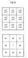
- the reference symbols ⁇ y11 ... ⁇ y33 denote the individual results in the y direction and ⁇ x11 ... ⁇ x33 the results in the x direction.
- three columns are integrated in the x and y directions in accordance with the number of grid elements. This creates nine grid elements, each with nine pairs of values ⁇ x m , ⁇ y m . The mean value from this then provides the final filing ⁇ x and ⁇ y.
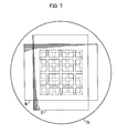
- FIG. 7 shows the two-dimensional grid on mask 16 and disk 17 centrally in a field of view 24 of the imaging optics, as well as two orthogonally arranged line-by-line scanning fields of two electronic image converters, for example, for realizing the parallel and orthogonal integration areas .
- the distance from the optical axis of the individual arrangement was used as the individual criterion.
- the results ⁇ x m , ⁇ y n from the individual grating elements can be weighted such that the results from the elements which are further away from the optical axis are weighted less. Due to the shifting of the grids on the mask and pane and into one another and as a result of the evaluation for ⁇ x m , ⁇ y n initially related to the individual grid elements, the accuracy with which a single line is detected can only be related to the small area of a grid element.
- the achievable overall accuracy results from the accuracy of the individual lines in connection with the number of limits per lattice element and the number of lattice elements according to statistical laws.
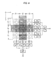
- FIG. 9 in turn shows the two-dimensional grid with the integration areas I and I ', as well as an arrangement of parallel processors ⁇ P1 to ⁇ P3 or, ⁇ P1' to ⁇ P3 'as well as the processors ⁇ P4' and ⁇ P4 for combination Formulation or averaging of the individual results in the x and y directions.
- the matrix structure for calculating the ⁇ x m , ⁇ y n in the individual elements offers the use of parallel processors ⁇ P, each of which is assigned an analog part for line-by-line integration and difference formation is. Further microprocessors take over the averaging of the results from the individual grid elements.
- FIG. 9 shows image processing of the two-dimensional grid that is as parallel as possible.
- An analog evaluation device (A1 to A3 or A1 'to A3') is provided for each column in the x and y directions, by means of which the integration and the difference formation are carried out.
- a microprocessor ( / üP1 to / uP3 or ⁇ P1 'to ⁇ P3') is again provided for each column in the x- and y-directions for the further digitized processing (center of gravity formation, averaging, summary and symmetry analysis) according to FIG. 1.
- the summary of the individual results from the individual arrangements in the x and y directions is carried out by the processors / uP4 or ⁇ P4 '.
- the arrows in the directions ⁇ x and ⁇ y indicate the output of the result of the position detection for the control elements.
- the rapid parallel information processing offers multiple repetitions of the measurement run and averaging from the individual results ( ⁇ x, ⁇ y).
Landscapes
- Engineering & Computer Science (AREA)
- Physics & Mathematics (AREA)
- General Physics & Mathematics (AREA)
- Multimedia (AREA)
- Signal Processing (AREA)
- Length Measuring Devices By Optical Means (AREA)
Applications Claiming Priority (4)
| Application Number | Priority Date | Filing Date | Title |
|---|---|---|---|
| DE2822269 | 1978-05-22 | ||
| DE19782822269 DE2822269C2 (de) | 1978-05-22 | 1978-05-22 | Verfahren zur automatischen Ausrichtung von zwei aufeinander einzujustierenden Objekten |
| DE19782846316 DE2846316A1 (de) | 1978-10-24 | 1978-10-24 | Verfahren und vorrichtung zur automatischen ausrichtung von zwei aufeinander einzujustierenden objekten |
| DE2846316 | 1978-10-24 |
Publications (3)
| Publication Number | Publication Date |
|---|---|
| EP0005462A2 true EP0005462A2 (fr) | 1979-11-28 |
| EP0005462A3 EP0005462A3 (en) | 1979-12-12 |
| EP0005462B1 EP0005462B1 (fr) | 1983-06-08 |
Family
ID=25774530
Family Applications (1)
| Application Number | Title | Priority Date | Filing Date |
|---|---|---|---|
| EP79101241A Expired EP0005462B1 (fr) | 1978-05-22 | 1979-04-24 | Procédé pour positionner deux objets à ajuster l'un sur l'autre |
Country Status (2)
| Country | Link |
|---|---|
| US (1) | US4253112A (fr) |
| EP (1) | EP0005462B1 (fr) |
Cited By (8)
| Publication number | Priority date | Publication date | Assignee | Title |
|---|---|---|---|---|
| DE3006578A1 (de) * | 1979-03-12 | 1980-09-25 | Perkin Elmer Corp | Bezugsbild zum ausrichten von masken fuer die herstellung von mikroschaltungen, verfahren zum ausrichten einer maske mit einer mikroschaltungsscheibe und verfahren und vorrichtung zum wahrnehmen und ausrichten von derartigen bezugsbildern |
| EP0051567A1 (fr) * | 1980-11-03 | 1982-05-12 | Jenoptik Jena G.m.b.H. | Dispositif pour l'ajustement automatique d'au moins un objet |
| EP0079070A1 (fr) * | 1981-11-09 | 1983-05-18 | American Semiconductor Equipment Technologies | Procédé d'alignement automatique des disques semi-conducteurs, procédé pour déterminer la place des bords et système d'alignement pour ces disques |
| EP0069529A3 (en) * | 1981-06-29 | 1983-11-16 | Fujitsu Limited | Chip alignment method |
| EP0096224A1 (fr) * | 1982-06-07 | 1983-12-21 | International Business Machines Corporation | Procédé de positionnement d'une série de masques utilisés dans la production IC |
| EP0226893A1 (fr) * | 1985-12-13 | 1987-07-01 | Siemens Aktiengesellschaft | Procédé de haute précision de mesure pour structures bidimensionnelles ainsi que masque de référence pour l'utilisation de ce procédé |
| EP0163199A3 (fr) * | 1984-05-29 | 1988-09-14 | Siemens Aktiengesellschaft | Procédé et appareil pour déterminer des défauts de recouvrement entre des structures qui sont appliquées successivement sur un substrat semi-conducteur |
| DE3911357A1 (de) * | 1989-04-07 | 1990-10-18 | Nokia Unterhaltungselektronik | Verfahren zum gegenseitigen justieren zweier bauteile einer anzeigeeinrichtung |
Families Citing this family (23)
| Publication number | Priority date | Publication date | Assignee | Title |
|---|---|---|---|---|
| US4327292A (en) * | 1980-05-13 | 1982-04-27 | Hughes Aircraft Company | Alignment process using serial detection of repetitively patterned alignment marks |
| US4431923A (en) * | 1980-05-13 | 1984-02-14 | Hughes Aircraft Company | Alignment process using serial detection of repetitively patterned alignment marks |
| US4580900A (en) * | 1982-04-02 | 1986-04-08 | Eaton Corporation | Auto focus alignment and measurement system and method |
| US4615621A (en) * | 1982-04-02 | 1986-10-07 | Eaton Corporation | Auto-focus alignment and measurement system and method |
| DE3319241A1 (de) * | 1983-04-30 | 1984-11-15 | Thomas Josef Heimbach GmbH & Co, 5160 Düren | Verfahren zum herstellen eines endlosen schlauchfilzes sowie vorrichtung zum durchfuehren dieses verfahrens |
| DE3372673D1 (en) * | 1983-09-23 | 1987-08-27 | Ibm Deutschland | Process and device for mutually aligning objects |
| US4593406A (en) * | 1984-01-16 | 1986-06-03 | The United States Of America As Represented By The United States Department Of Energy | Automatic image acquisition processor and method |
| US4860374A (en) * | 1984-04-19 | 1989-08-22 | Nikon Corporation | Apparatus for detecting position of reference pattern |
| US4688088A (en) * | 1984-04-20 | 1987-08-18 | Canon Kabushiki Kaisha | Position detecting device and method |
| US4703185A (en) * | 1984-12-20 | 1987-10-27 | Siemens Aktiengesellschaft | Arrangement for optical imaging of two subjects located in different object planes |
| EP0253283A3 (fr) * | 1986-07-15 | 1988-07-20 | Siemens Aktiengesellschaft | Dispositif d'exposition de plaques de semi-conducteur au moyen de radiation synchrotron dans un appareil de lithographie |
| DE3623891A1 (de) * | 1986-07-15 | 1988-01-28 | Siemens Ag | Anordnung zur genauen gegenseitigen ausrichtung einer maske und einer halbleiterscheibe in einem lithographiegeraet und verfahren zu ihrem betrieb |
| US5022089A (en) * | 1990-01-19 | 1991-06-04 | Wilson Monti R | Method and apparatus for fast registration using crosshair register marks |
| US5621813A (en) * | 1993-01-14 | 1997-04-15 | Ultratech Stepper, Inc. | Pattern recognition alignment system |
| US5742701A (en) * | 1994-02-15 | 1998-04-21 | Matsushita Electric Industrial Co., Ltd. | Alignment detection apparatus |
| ITBO940153A1 (it) * | 1994-04-12 | 1995-10-12 | Gd Spa | Metodo per il controllo ottico di prodotti. |
| DE19545721C2 (de) * | 1995-12-07 | 2003-02-20 | Deutsche Telekom Ag | Verfahren und Vorrichtung zum Herstellen und präzisen Positionieren von optischen Mikrokomponenten auf einer über einer optischen Einrichtung |
| US7106895B1 (en) * | 1999-05-05 | 2006-09-12 | Kla-Tencor | Method and apparatus for inspecting reticles implementing parallel processing |
| US6889162B1 (en) * | 2000-03-07 | 2005-05-03 | Koninklijke Philips Electronics N.V. | Wafer target design and method for determining centroid of wafer target |
| US6783320B2 (en) * | 2001-03-21 | 2004-08-31 | International Automated Systems, Inc. | Pressurized gas turbine engine with electrothermodynamic enhancement |
| JP4307054B2 (ja) * | 2002-11-29 | 2009-08-05 | パナソニック株式会社 | 部品撮像装置 |
| US7215808B2 (en) * | 2004-05-04 | 2007-05-08 | Kla-Tencor Technologies Corporation | High throughout image for processing inspection images |
| JP4449697B2 (ja) * | 2004-10-26 | 2010-04-14 | 株式会社ニコン | 重ね合わせ検査システム |
Family Cites Families (4)
| Publication number | Priority date | Publication date | Assignee | Title |
|---|---|---|---|---|
| DE1919991C3 (de) | 1969-04-19 | 1973-11-29 | Licentia Patent-Verwaltungs-Gmbh, 6000 Frankfurt | Anordnung zur automatischen Aus richtung von zwei aufeinander einzu justierenden Objekten |
| JPS51140488A (en) * | 1975-05-30 | 1976-12-03 | Hitachi Ltd | Mask alignment device |
| US3988535A (en) * | 1975-11-04 | 1976-10-26 | Western Electric Company, Inc. | Automated positioning |
| US4097750A (en) * | 1977-03-18 | 1978-06-27 | General Motors Corporation | Method of orienting objects using optically smeared images |
-
1979
- 1979-04-24 EP EP79101241A patent/EP0005462B1/fr not_active Expired
- 1979-05-21 US US06/040,540 patent/US4253112A/en not_active Expired - Lifetime
Cited By (10)
| Publication number | Priority date | Publication date | Assignee | Title |
|---|---|---|---|---|
| DE3006578A1 (de) * | 1979-03-12 | 1980-09-25 | Perkin Elmer Corp | Bezugsbild zum ausrichten von masken fuer die herstellung von mikroschaltungen, verfahren zum ausrichten einer maske mit einer mikroschaltungsscheibe und verfahren und vorrichtung zum wahrnehmen und ausrichten von derartigen bezugsbildern |
| EP0051567A1 (fr) * | 1980-11-03 | 1982-05-12 | Jenoptik Jena G.m.b.H. | Dispositif pour l'ajustement automatique d'au moins un objet |
| EP0069529A3 (en) * | 1981-06-29 | 1983-11-16 | Fujitsu Limited | Chip alignment method |
| EP0079070A1 (fr) * | 1981-11-09 | 1983-05-18 | American Semiconductor Equipment Technologies | Procédé d'alignement automatique des disques semi-conducteurs, procédé pour déterminer la place des bords et système d'alignement pour ces disques |
| US4475122A (en) * | 1981-11-09 | 1984-10-02 | Tre Semiconductor Equipment Corporation | Automatic wafer alignment technique |
| EP0143893A1 (fr) * | 1981-11-09 | 1985-06-12 | American Semiconductor Equipment Technologies | Procédé d'alignement automatique de tranches de semi-conducteur, procédé pour déterminer la position des bords et système d'alignement pour ces tranches |
| EP0096224A1 (fr) * | 1982-06-07 | 1983-12-21 | International Business Machines Corporation | Procédé de positionnement d'une série de masques utilisés dans la production IC |
| EP0163199A3 (fr) * | 1984-05-29 | 1988-09-14 | Siemens Aktiengesellschaft | Procédé et appareil pour déterminer des défauts de recouvrement entre des structures qui sont appliquées successivement sur un substrat semi-conducteur |
| EP0226893A1 (fr) * | 1985-12-13 | 1987-07-01 | Siemens Aktiengesellschaft | Procédé de haute précision de mesure pour structures bidimensionnelles ainsi que masque de référence pour l'utilisation de ce procédé |
| DE3911357A1 (de) * | 1989-04-07 | 1990-10-18 | Nokia Unterhaltungselektronik | Verfahren zum gegenseitigen justieren zweier bauteile einer anzeigeeinrichtung |
Also Published As
| Publication number | Publication date |
|---|---|
| US4253112A (en) | 1981-02-24 |
| EP0005462B1 (fr) | 1983-06-08 |
| EP0005462A3 (en) | 1979-12-12 |
Similar Documents
| Publication | Publication Date | Title |
|---|---|---|
| EP0005462B1 (fr) | Procédé pour positionner deux objets à ajuster l'un sur l'autre | |
| DE69610023T2 (de) | Analog hochauflösender Laserstrahlungsdetektor | |
| DE68926664T2 (de) | Detektoranordnung und Beleuchtungssystem für einen Strichkode-Abtaster mit grosser Tiefenschärfe | |
| DE69737862T2 (de) | Automatische justierung eines energiefiltrierenden transmissionselektronenmikroskops | |
| EP0689700B1 (fr) | Procede d'acquisition de codes a barres | |
| DE3785891T2 (de) | Umgekehrtes dunkelfeld-ausrichtsystem fuer einen lithographischen ausrichtscanner. | |
| DE3410421C2 (de) | Verfahren und Vorrichtung zum Erfassen einer linienförmigen ersten Markierung und einer linienförmigen zweiten Markierung | |
| DE2939044A1 (de) | Einrichtung fuer elektronenstrahllithographie | |
| CH656743A5 (de) | Verfahren und vorrichtung zum ausrichten einer maske bei der herstellung von mikroschaltungen. | |
| EP2929332B1 (fr) | Dispositif d'inspection | |
| DE2549905C3 (de) | Vorrichtung zur Scharfeinstellung eines Objektivs | |
| DE2917253C2 (fr) | ||
| DE2822269C2 (de) | Verfahren zur automatischen Ausrichtung von zwei aufeinander einzujustierenden Objekten | |
| DE69128667T2 (de) | Positionsbestimmungsmethode | |
| DE69803044T2 (de) | Optisches gerät zur kontaktlosen messung des abstandes zu einer lichtquelle | |
| DE10323088A1 (de) | Positionsmesseinrichtung | |
| DE3312203C2 (fr) | ||
| DE3323836A1 (de) | Verfahren zur festlegung einer koordinate auf einer oberflaeche eines festkoerpers und vorrichtung zur durchfuehrung eines solchen verfahrens | |
| DE2526110C3 (de) | Vorrichtung zum Messen kleiner Auslenkungen eines Lichtbündels | |
| EP0218865B1 (fr) | Dispositif pour la détection sans contact de défauts dans des surfaces non structurées | |
| DE3413605C2 (fr) | ||
| DE2921857A1 (de) | Optisches empfangssystem | |
| DE1447286A1 (de) | Digitale Strahlablenkeinrichtung | |
| DE2937741C2 (de) | Verfahren und Vorrichtung zur opto-elektronischen Vermessung von Mikrostrukturen, insbesondere auf Masken und Scheiben der Halbleitertechnik | |
| DE2846316A1 (de) | Verfahren und vorrichtung zur automatischen ausrichtung von zwei aufeinander einzujustierenden objekten |
Legal Events
| Date | Code | Title | Description |
|---|---|---|---|
| PUAI | Public reference made under article 153(3) epc to a published international application that has entered the european phase |
Free format text: ORIGINAL CODE: 0009012 |
|
| PUAL | Search report despatched |
Free format text: ORIGINAL CODE: 0009013 |
|
| AK | Designated contracting states |
Designated state(s): CH FR GB NL |
|
| AK | Designated contracting states |
Designated state(s): CH FR GB NL |
|
| 17P | Request for examination filed | ||
| GRAA | (expected) grant |
Free format text: ORIGINAL CODE: 0009210 |
|
| AK | Designated contracting states |
Designated state(s): CH FR GB NL |
|
| ET | Fr: translation filed | ||
| PLBE | No opposition filed within time limit |
Free format text: ORIGINAL CODE: 0009261 |
|
| STAA | Information on the status of an ep patent application or granted ep patent |
Free format text: STATUS: NO OPPOSITION FILED WITHIN TIME LIMIT |
|
| 26N | No opposition filed | ||
| PGFP | Annual fee paid to national office [announced via postgrant information from national office to epo] |
Ref country code: GB Payment date: 19980310 Year of fee payment: 20 |
|
| PGFP | Annual fee paid to national office [announced via postgrant information from national office to epo] |
Ref country code: NL Payment date: 19980420 Year of fee payment: 20 Ref country code: FR Payment date: 19980420 Year of fee payment: 20 |
|
| PGFP | Annual fee paid to national office [announced via postgrant information from national office to epo] |
Ref country code: CH Payment date: 19980709 Year of fee payment: 20 |
|
| PG25 | Lapsed in a contracting state [announced via postgrant information from national office to epo] |
Ref country code: GB Free format text: LAPSE BECAUSE OF NON-PAYMENT OF DUE FEES Effective date: 19990423 Ref country code: CH Free format text: LAPSE BECAUSE OF EXPIRATION OF PROTECTION Effective date: 19990423 |
|
| PG25 | Lapsed in a contracting state [announced via postgrant information from national office to epo] |
Ref country code: NL Free format text: LAPSE BECAUSE OF EXPIRATION OF PROTECTION Effective date: 19990424 |
|
| REG | Reference to a national code |
Ref country code: CH Ref legal event code: PL |
|
| REG | Reference to a national code |
Ref country code: GB Ref legal event code: PE20 Effective date: 19990423 |
|
| NLV7 | Nl: ceased due to reaching the maximum lifetime of a patent |
Effective date: 19990424 |