EP0096224A1 - Procédé de positionnement d'une série de masques utilisés dans la production IC - Google Patents
Procédé de positionnement d'une série de masques utilisés dans la production IC Download PDFInfo
- Publication number
- EP0096224A1 EP0096224A1 EP83104481A EP83104481A EP0096224A1 EP 0096224 A1 EP0096224 A1 EP 0096224A1 EP 83104481 A EP83104481 A EP 83104481A EP 83104481 A EP83104481 A EP 83104481A EP 0096224 A1 EP0096224 A1 EP 0096224A1
- Authority
- EP
- European Patent Office
- Prior art keywords
- mask
- alignment
- fields
- masks
- positioning method
- Prior art date
- Legal status (The legal status is an assumption and is not a legal conclusion. Google has not performed a legal analysis and makes no representation as to the accuracy of the status listed.)
- Granted
Links
- 238000000034 method Methods 0.000 title claims abstract description 18
- 238000004519 manufacturing process Methods 0.000 title description 2
- 238000013461 design Methods 0.000 claims description 7
- 235000012431 wafers Nutrition 0.000 description 7
- 238000005259 measurement Methods 0.000 description 4
- 239000004065 semiconductor Substances 0.000 description 4
- 238000012937 correction Methods 0.000 description 3
- 229920002120 photoresistant polymer Polymers 0.000 description 2
- 230000009286 beneficial effect Effects 0.000 description 1
- 230000007423 decrease Effects 0.000 description 1
- 230000000694 effects Effects 0.000 description 1
- 239000011521 glass Substances 0.000 description 1
- 238000004377 microelectronic Methods 0.000 description 1
- 238000012544 monitoring process Methods 0.000 description 1
- 238000002161 passivation Methods 0.000 description 1
- 238000012163 sequencing technique Methods 0.000 description 1
Images


Classifications
-
- G—PHYSICS
- G03—PHOTOGRAPHY; CINEMATOGRAPHY; ANALOGOUS TECHNIQUES USING WAVES OTHER THAN OPTICAL WAVES; ELECTROGRAPHY; HOLOGRAPHY
- G03F—PHOTOMECHANICAL PRODUCTION OF TEXTURED OR PATTERNED SURFACES, e.g. FOR PRINTING, FOR PROCESSING OF SEMICONDUCTOR DEVICES; MATERIALS THEREFOR; ORIGINALS THEREFOR; APPARATUS SPECIALLY ADAPTED THEREFOR
- G03F9/00—Registration or positioning of originals, masks, frames, photographic sheets or textured or patterned surfaces, e.g. automatically
- G03F9/70—Registration or positioning of originals, masks, frames, photographic sheets or textured or patterned surfaces, e.g. automatically for microlithography
- G03F9/7073—Alignment marks and their environment
- G03F9/7076—Mark details, e.g. phase grating mark, temporary mark
-
- G—PHYSICS
- G03—PHOTOGRAPHY; CINEMATOGRAPHY; ANALOGOUS TECHNIQUES USING WAVES OTHER THAN OPTICAL WAVES; ELECTROGRAPHY; HOLOGRAPHY
- G03F—PHOTOMECHANICAL PRODUCTION OF TEXTURED OR PATTERNED SURFACES, e.g. FOR PRINTING, FOR PROCESSING OF SEMICONDUCTOR DEVICES; MATERIALS THEREFOR; ORIGINALS THEREFOR; APPARATUS SPECIALLY ADAPTED THEREFOR
- G03F1/00—Originals for photomechanical production of textured or patterned surfaces, e.g., masks, photo-masks, reticles; Mask blanks or pellicles therefor; Containers specially adapted therefor; Preparation thereof
- G03F1/38—Masks having auxiliary features, e.g. special coatings or marks for alignment or testing; Preparation thereof
- G03F1/42—Alignment or registration features, e.g. alignment marks on the mask substrates
-
- G—PHYSICS
- G03—PHOTOGRAPHY; CINEMATOGRAPHY; ANALOGOUS TECHNIQUES USING WAVES OTHER THAN OPTICAL WAVES; ELECTROGRAPHY; HOLOGRAPHY
- G03F—PHOTOMECHANICAL PRODUCTION OF TEXTURED OR PATTERNED SURFACES, e.g. FOR PRINTING, FOR PROCESSING OF SEMICONDUCTOR DEVICES; MATERIALS THEREFOR; ORIGINALS THEREFOR; APPARATUS SPECIALLY ADAPTED THEREFOR
- G03F1/00—Originals for photomechanical production of textured or patterned surfaces, e.g., masks, photo-masks, reticles; Mask blanks or pellicles therefor; Containers specially adapted therefor; Preparation thereof
- G03F1/68—Preparation processes not covered by groups G03F1/20 - G03F1/50
- G03F1/70—Adapting basic layout or design of masks to lithographic process requirements, e.g., second iteration correction of mask patterns for imaging
Definitions
- This invention relates generally to integrated circuit fabrication and and more particularly to the mark and mask sets used to produce such integrated circuits.
- photo-lithographic techniques are widely used to produce integrated circuits or fields of circuits in semiconductor wafers. These wafers can contain upwards of two hundred distinct fields.
- the used photo techniques require that the devices forming the circuits in each field be created by using a series or set of masks. Each mask is used to form a portion of the circuit or field. By the proper sequencing of the masks the circuit or field is ultimately formed.
- a first mask is used to define the transistor's collector region, the second mask to define its base region, a third mask to define its emitter region, a fourth mask to define via openings in any passivation layer overlying these regions and a fifth mask to define the contacts to the various regions.
- These or other masks may be used to define other circuit elements such as sources or claims for FET devices or resistors.
- each mask is provided with two separate symmetrical alignment areas each containing one or more alignment marks.
- the wafer is exposed to the first mask in the set to define on. the surface of the wafer the alignment marks of the first mask.
- Each subsequent mask is then aligned with respect to this first established mask.
- each field on the mask is independently created
- corresponding fields on each mask in the set can be slightly misaligned with respect to each other. This misalignment is, in the present art, compensated for by making the circuit elements in each mask larger than is necessitated by electrical requirements.
- the invention as claimed is intended to remedy the above drawbacks. It is the primary goal of the present invention to produce photolithographic mask sets for creating integrated circuits which will have minimum mismatch between the respective fields on the various masks in the sets. This is basically achieved by aligning each mask as formed to a known standard, forming an alignment indicator in the form of a scale on each mask and forming a vernier scale on each subsequent mask which indicates which element on the vernier scale must be aligned with the scale on the previous mask to minimize mismatch between each of the fields on the mask being aligned with respect to the fields of any previously used mask.
- FIG. 1 shows a typical mask used in the producticn of semiconductor integrated circuits.
- Each mask is made on a square glass plate 10 with an image area defined by a circle 11 of a size substantially identical to the size of the semiconductor wafer being treated.
- Such masks have a number of image fields 12 which contain the images to be produced in the photoresist layer deposited on the semiconductor body being exposed through the mask.
- the images on the mask can be either positive or negative depending on the type of photoresist used.
- In addition to the image fields 12 there is, within image area 11, at least two alignment fields 13a and 13b.
- Such masks are normally produced using so-called step and repeat cameras which are designed to precisely position the image fields in very precise locations with repeat to the left edge and the bottom edge of the chip.
- step and repeat cameras which are designed to precisely position the image fields in very precise locations with repeat to the left edge and the bottom edge of the chip.
- the plate 10 is 8 inches by 8 inches (203 x 203 mm) and that each field has a centrally located alignment mark. This is ideally positioned on the mask everywhere the inch grid coordinates cross.
- these field centers can be positioned as much as twenty or more microinches (0,5 urn or more) in any direction from its desired position. It is thus the purpose of this invention to attempt to minimize the effect of these positioning inaccuracies especially when arranging the mask in sets.
- Each of these alignment fields 13a and 13b contain at least one alignment mark and usually contains at least one mark for each mask in the final set. These marks can take many forms.
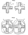
- Fig. 2 illustrates one such set of such alignment marks 14a and 14b as might be found in the respective alignment fields 13a and 13b of a first mask. Alignment mark 14a would be in field 13a and mark 14b would be found in field 13b.
- Each mark is a mirror image of the other and is shown comprised of several nested, greek crosses 15, 16 and 17 with a number of parallel bars 18 in an arm, each equally spaced from the adjacent marks in the arm.
- Fig. 3 illustrates one such set of alignment marks 19a and 19b as might be found in the respective alignment fields 13a and l3b of a second mask (not shown) that is to be aligned to the first mask of Fig. 1.
- These alignment marks comprises a series of generally L-shaped lines 20.
- the alignment marks of the second mask should have a periodicity either increasing or declining spacing different from the spacing of the marks 14a and 14b of the first mask.
- the most central marks on such mask set represented the zero position, thus when these sets were to be precisely aligned with each other, the central marks 22a, 22b, 22c, 22d of set 19a would be centered on the respective marks 21a, 21b, 21c, and 21d of mask 14a.
- the present invention treats the second set of alignment marks 19a and 19b to indicate which mark of the vernier must be centered on the corresponding mark of the first set as to minimize mismatch between the masks. For example in Fig. 6, the fourth vernier mark 23a of the right arm and the sixth vernier mark 23b of the lower arm is centered on the corresponding mark 24a and 24b of the first mask set. This will become clearer as the detailed description of the preferred procedures is explained below.
- the actual position of the center of each field and the centroid of all the fields on each mark must be determined.
- the first mask must be placed in an X-Y coordinate measuring system such as is sold by Nikon Corporation under the model name 2I.
- an X-Y coordinate measuring system such as is sold by Nikon Corporation under the model name 2I.
- Another similar X-Y coordinate measuring system is described in detail in an article by P. H. Coffy, entitled “An X-Y Measurement System", which appears on pages 1-14 in the Kodak Microelectronics Seminar Proceedings, dated October 1-3, 1978, San Diego, California.
- a first mask 38 is placed in the stage 39 of a measuring system. Since such measuring systems are well known and commercially available, its details are not shown.
- the mask 38 is shown as slightly mispositioned and skewed on the stage 39.
- the lower left corner 40 of the mask 38 is shown spaced apart from the internal corner 41 of the stage 39, into which the corner 40 should fit snugly.
- the X and Y coordinates of the center of alignment mark of the alignment field 42 are precisely located and measured by the machine and indicated below as X' and Y' with respect to the machine zero position 41, i.e., in terms of the machine coordinates.
- the center of the alignment mark appearing in the other alignment fields 43 is also measured in these machine coordinates.
- the angle which is the angle between edge of mask 38 and the edge of the stage 39.
- the position of the center line between the two alignment fields 42 and 43 can be established in mask coordinates indicated below as X and Y in accordance with the following equations.
- the center of each of the other fields on the mask 38 is measured and established with respect to the mask zero position.
- centroid of this data i. e., the actual center of the mass of all the measured fields, is established with respect to the design center of the plate.
- This delta is now added to the measured values of the alignment fields 42 and 43 to reset the alignment fields so that the measured centroid will align with the design centroid.
- next mask in the mask set is now treated in a similar way so that again the actual position of the center of each field and the centroid of all the fields on the mask can be determined.
- This second mask is also placed in the X-Y coordinate measuring system.
- the second mask 58 is placed in the stage 39 of the measuring system.
- mask 58 is shown as properly fitted on the stage 39.
- the lower left corner 40 of the plate 58 is shown as snugly fitted in the internal corner 41 of the stage 39.
- the machine coordinates of the center of alignment mark of the alignment field 59 is precisely located and measured by the machine with respect to the machine zero position 41, i. e., in terms of the machine coordinates.
- the center of the alignment mask appearing in the other alignment field 60 is also measured in the machine coordinates.
- the angle between the edge of the mask 58 and the edge of the stage 39 in this case is zero.
- the center of each of the alignment fields is not only related to the corner 40 of the mask on which the fields appear, but also are the same with respect to the mask zero position.
- This delta is now added to the measured values of the alignment fields 59 and 60 to shift these alignment fields so that the measured centroid will align with the design centroid.
- the customization process is to mark the alignment vernier to indicate which vernier to align.
- the ver- niers thus marked are superimposed on the alignment marks of the first mask as shown in Fig. 6.
- the alignment mark in field 59 of the second mask is superimposed over the alignment mark 42 of the first mask such that the treated mark 23a is centrally positioned over the fourth mark 24a in alignment field 42 and the treated mark 23b is positioned over the sixth mark 24b of alignment field 42.
- the mark in field 60 is positioned over the mark in field 43.
- the vernier 73 of the mark in field 60 is aligned with the vernier 77 of the mark in field 43.
- vernier 74 is aligned with the vernier 78.
- the overall average error of the mask fields on each mask set is brought to zero and the overall mismatch between the fields is minimized and a best overlay achieved.
Landscapes
- Physics & Mathematics (AREA)
- General Physics & Mathematics (AREA)
- Exposure And Positioning Against Photoresist Photosensitive Materials (AREA)
- Exposure Of Semiconductors, Excluding Electron Or Ion Beam Exposure (AREA)
- Preparing Plates And Mask In Photomechanical Process (AREA)
- Control Of Position Or Direction (AREA)
Applications Claiming Priority (2)
| Application Number | Priority Date | Filing Date | Title |
|---|---|---|---|
| US06/385,591 US4388386A (en) | 1982-06-07 | 1982-06-07 | Mask set mismatch |
| US385591 | 1982-06-07 |
Publications (2)
| Publication Number | Publication Date |
|---|---|
| EP0096224A1 true EP0096224A1 (fr) | 1983-12-21 |
| EP0096224B1 EP0096224B1 (fr) | 1986-10-29 |
Family
ID=23522055
Family Applications (1)
| Application Number | Title | Priority Date | Filing Date |
|---|---|---|---|
| EP83104481A Expired EP0096224B1 (fr) | 1982-06-07 | 1983-05-06 | Procédé de positionnement d'une série de masques utilisés dans la production IC |
Country Status (4)
| Country | Link |
|---|---|
| US (1) | US4388386A (fr) |
| EP (1) | EP0096224B1 (fr) |
| JP (1) | JPS58216422A (fr) |
| DE (1) | DE3367286D1 (fr) |
Cited By (1)
| Publication number | Priority date | Publication date | Assignee | Title |
|---|---|---|---|---|
| EP0550173A1 (fr) * | 1991-12-30 | 1993-07-07 | AT&T Corp. | Circuits intégrés |
Families Citing this family (25)
| Publication number | Priority date | Publication date | Assignee | Title |
|---|---|---|---|---|
| US4474465A (en) * | 1982-09-07 | 1984-10-02 | International Business Machines Corporation | Method and apparatus for making a mask conforming to a ceramic substrate metallization pattern |
| US4606643A (en) * | 1983-06-20 | 1986-08-19 | The Perkin-Elmer Corporation | Fine alignment system |
| JPS6083328A (ja) * | 1983-10-13 | 1985-05-11 | Fujitsu Ltd | フオトマスクの検査方法 |
| JPS6085523A (ja) * | 1983-10-17 | 1985-05-15 | Fujitsu Ltd | マスク形成方法 |
| US4527333A (en) * | 1984-01-23 | 1985-07-09 | Graphic Arts Technical Foundation | Device for indicating a quantitative change in dot area of an image in a printing process and the method of making the same |
| JPH0712194B2 (ja) * | 1984-07-13 | 1995-02-08 | キヤノン株式会社 | 画像処理装置 |
| JPS633416A (ja) * | 1986-06-24 | 1988-01-08 | Sony Corp | 半導体装置 |
| US4750836A (en) * | 1986-09-18 | 1988-06-14 | Rca Corporation | Method of measuring misalignment between superimposed patterns |
| US4768883A (en) * | 1986-11-07 | 1988-09-06 | Motorola Inc. | Alignment reticle for a semiconductor wafer stepper system and method of use |
| DE3911357A1 (de) * | 1989-04-07 | 1990-10-18 | Nokia Unterhaltungselektronik | Verfahren zum gegenseitigen justieren zweier bauteile einer anzeigeeinrichtung |
| JPH0444307A (ja) * | 1990-06-12 | 1992-02-14 | Nec Corp | 半導体装置の製造方法 |
| US5280437A (en) * | 1991-06-28 | 1994-01-18 | Digital Equipment Corporation | Structure and method for direct calibration of registration measurement systems to actual semiconductor wafer process topography |
| US5747200A (en) * | 1995-08-23 | 1998-05-05 | Micrel, Incorporated | Mask structure having offset patterns for alignment |
| JP3518097B2 (ja) * | 1995-09-29 | 2004-04-12 | 株式会社ニコン | 荷電粒子線転写装置,パターン分割方法,マスクおよび荷電粒子線転写方法 |
| JPH10122817A (ja) * | 1996-10-16 | 1998-05-15 | Nec Corp | レーザマスクリペアでのマスクの位置合せ方法 |
| JP3287321B2 (ja) | 1998-12-03 | 2002-06-04 | 日本電気株式会社 | 半導体装置の製造方法 |
| DE19817714C5 (de) * | 1998-04-21 | 2011-06-30 | Vistec Semiconductor Systems GmbH, 35781 | Verfahren zur Messung der Lage von Strukturen auf einer Maskenoberfläche |
| JP3761357B2 (ja) * | 1999-02-22 | 2006-03-29 | 株式会社東芝 | 露光量モニタマスク、露光量調整方法及び半導体装置の製造方法 |
| JP5180419B2 (ja) * | 2000-08-30 | 2013-04-10 | ケーエルエー−テンカー・コーポレーション | 重ね合わせマーク、重ね合わせマークの設計方法および重ね合わせ測定の方法 |
| US6737205B2 (en) * | 2002-04-30 | 2004-05-18 | Motorola, Inc. | Arrangement and method for transferring a pattern from a mask to a wafer |
| FR2875624A1 (fr) * | 2004-09-23 | 2006-03-24 | St Microelectronics Sa | Generation deterministe d'un numero d'identifiant d'un circuit integre |
| CN100552543C (zh) * | 2006-07-18 | 2009-10-21 | 友达光电股份有限公司 | 用于彩色滤光片工艺的光掩模 |
| DE102007049100B4 (de) * | 2007-10-11 | 2009-07-16 | Vistec Semiconductor Systems Gmbh | Verfahren zur Bestimmung der Centrality von Masken |
| TWI401529B (zh) * | 2008-06-27 | 2013-07-11 | Au Optronics Corp | 光罩上的對位標尺及應用對位標尺的遮蔽件位置確認方法 |
| US9230050B1 (en) | 2014-09-11 | 2016-01-05 | The United States Of America, As Represented By The Secretary Of The Air Force | System and method for identifying electrical properties of integrate circuits |
Citations (2)
| Publication number | Priority date | Publication date | Assignee | Title |
|---|---|---|---|---|
| EP0005462A2 (fr) * | 1978-05-22 | 1979-11-28 | Siemens Aktiengesellschaft | Procédé pour positionner deux objets à ajuster l'un sur l'autre |
| EP0030878A1 (fr) * | 1979-12-18 | 1981-06-24 | Thomson-Csf | Système optique d'alignement de deux motifs et photorépéteur mettant en oeuvre un tel système |
Family Cites Families (6)
| Publication number | Priority date | Publication date | Assignee | Title |
|---|---|---|---|---|
| US4070117A (en) * | 1972-06-12 | 1978-01-24 | Kasper Instruments, Inc. | Apparatus for the automatic alignment of two superimposed objects, e.g. a semiconductor wafer and mask |
| JPS5212577A (en) * | 1975-07-21 | 1977-01-31 | Nippon Kogaku Kk <Nikon> | Automatic location device |
| DE2622283A1 (de) * | 1976-05-19 | 1977-12-08 | Bosch Gmbh Robert | Verfahren zur lokalisierung eines festkoerperplaettchens und festkoerperplaettchen zur durchfuehrung des verfahrens |
| NL7606548A (nl) * | 1976-06-17 | 1977-12-20 | Philips Nv | Werkwijze en inrichting voor het uitrichten van een i.c.-patroon ten opzichte van een halfgelei- dend substraat. |
| US4134066A (en) * | 1977-03-24 | 1979-01-09 | International Business Machines Corporation | Wafer indexing system using a grid pattern and coding and orientation marks in each grid cell |
| US4193687A (en) * | 1978-06-05 | 1980-03-18 | Rockwell International Corporation | High resolution alignment technique and apparatus |
-
1982
- 1982-06-07 US US06/385,591 patent/US4388386A/en not_active Expired - Lifetime
-
1983
- 1983-03-29 JP JP58051712A patent/JPS58216422A/ja active Granted
- 1983-05-06 EP EP83104481A patent/EP0096224B1/fr not_active Expired
- 1983-05-06 DE DE8383104481T patent/DE3367286D1/de not_active Expired
Patent Citations (2)
| Publication number | Priority date | Publication date | Assignee | Title |
|---|---|---|---|---|
| EP0005462A2 (fr) * | 1978-05-22 | 1979-11-28 | Siemens Aktiengesellschaft | Procédé pour positionner deux objets à ajuster l'un sur l'autre |
| EP0030878A1 (fr) * | 1979-12-18 | 1981-06-24 | Thomson-Csf | Système optique d'alignement de deux motifs et photorépéteur mettant en oeuvre un tel système |
Non-Patent Citations (4)
| Title |
|---|
| ELECTRONICS, 15th February 1979, pages 68,70 * |
| IBM TECHNICAL DISCLOSURE BULLETIN, vol. 13, no. 4, September 1970, pages 955-956, New York, USA * |
| IEEE TRANSACTIONS ON ELECTRON DEVICES, vol. ED-27, no. 12, December 1980, pages 2304-2312, IEEE, New York, USA * |
| SOLID-STATE TECHNOLOGY, vol. 25, no. 5, May 1982, pages 111-115, New York, USA * |
Cited By (1)
| Publication number | Priority date | Publication date | Assignee | Title |
|---|---|---|---|---|
| EP0550173A1 (fr) * | 1991-12-30 | 1993-07-07 | AT&T Corp. | Circuits intégrés |
Also Published As
| Publication number | Publication date |
|---|---|
| JPS6227729B2 (fr) | 1987-06-16 |
| JPS58216422A (ja) | 1983-12-16 |
| US4388386A (en) | 1983-06-14 |
| DE3367286D1 (en) | 1986-12-04 |
| EP0096224B1 (fr) | 1986-10-29 |
Similar Documents
| Publication | Publication Date | Title |
|---|---|---|
| US4388386A (en) | Mask set mismatch | |
| EP0061536B1 (fr) | Procédé de fabrication d'un dispositif semiconducteur à repères d'alignement améliorés et repères d'alignment pour ledit procédé | |
| US5877861A (en) | Method for overlay control system | |
| US5783341A (en) | Alignment for layer formation through determination of target values for translation, rotation and magnification | |
| KR950003892B1 (ko) | 웨이퍼 묘화장치 | |
| US6239858B1 (en) | Exposure method, exposure apparatus and semiconductor device manufactured by using the exposure apparatus | |
| JP2000182934A (ja) | 半導体ウエハの位置合わせ方法 | |
| JPS62145103A (ja) | 二次元パタ−ンの高精密位置測定方法および基準マスク | |
| CN101533229B (zh) | 用于投影曝光装置的标线以及使用它的曝光方法 | |
| US4343878A (en) | System for providing photomask alignment keys in semiconductor integrated circuit processing | |
| EP1128215A2 (fr) | Jeu de marques d'alignement et méthode de mesure de la précision d'alignement | |
| JPH08274004A (ja) | 半導体装置 | |
| JP2003257828A (ja) | 半導体装置の製造方法 | |
| US6309944B1 (en) | Overlay matching method which eliminates alignment induced errors and optimizes lens matching | |
| TWI302348B (fr) | ||
| JP2002134397A (ja) | フォトマスク、半導体装置、半導体チップパターンの露光方法、チップアライメント精度検査装置 | |
| US7136520B2 (en) | Method of checking alignment accuracy of patterns on stacked semiconductor layers | |
| JPH0620909A (ja) | 露光方法及び薄膜多層基板 | |
| US5665645A (en) | Method of manufacturing a semiconductor device using reticles | |
| JPH0831404B2 (ja) | 半導体装置の製造方法 | |
| JPH0547621A (ja) | 半導体製造プロセスにおけるマスク合わせ方法 | |
| KR0116281Y1 (ko) | 반도체 체조장치의 개량 마스크 | |
| JP2617613B2 (ja) | 縮小投影露光装置用レチクル | |
| JPS59161033A (ja) | フオトマスク | |
| JPH0770575B2 (ja) | 半導体装置 |
Legal Events
| Date | Code | Title | Description |
|---|---|---|---|
| PUAI | Public reference made under article 153(3) epc to a published international application that has entered the european phase |
Free format text: ORIGINAL CODE: 0009012 |
|
| AK | Designated contracting states |
Designated state(s): DE FR GB IT |
|
| 17P | Request for examination filed |
Effective date: 19840426 |
|
| GRAA | (expected) grant |
Free format text: ORIGINAL CODE: 0009210 |
|
| AK | Designated contracting states |
Kind code of ref document: B1 Designated state(s): DE FR GB IT |
|
| REF | Corresponds to: |
Ref document number: 3367286 Country of ref document: DE Date of ref document: 19861204 |
|
| ET | Fr: translation filed | ||
| ITF | It: translation for a ep patent filed | ||
| PLBE | No opposition filed within time limit |
Free format text: ORIGINAL CODE: 0009261 |
|
| STAA | Information on the status of an ep patent application or granted ep patent |
Free format text: STATUS: NO OPPOSITION FILED WITHIN TIME LIMIT |
|
| 26N | No opposition filed | ||
| ITTA | It: last paid annual fee | ||
| PGFP | Annual fee paid to national office [announced via postgrant information from national office to epo] |
Ref country code: GB Payment date: 19930427 Year of fee payment: 11 Ref country code: FR Payment date: 19930427 Year of fee payment: 11 |
|
| PGFP | Annual fee paid to national office [announced via postgrant information from national office to epo] |
Ref country code: DE Payment date: 19930525 Year of fee payment: 11 |
|
| PG25 | Lapsed in a contracting state [announced via postgrant information from national office to epo] |
Ref country code: GB Effective date: 19940506 |
|
| GBPC | Gb: european patent ceased through non-payment of renewal fee |
Effective date: 19940506 |
|
| PG25 | Lapsed in a contracting state [announced via postgrant information from national office to epo] |
Ref country code: FR Effective date: 19950131 |
|
| PG25 | Lapsed in a contracting state [announced via postgrant information from national office to epo] |
Ref country code: DE Effective date: 19950201 |
|
| REG | Reference to a national code |
Ref country code: FR Ref legal event code: ST |