EP0006702A1 - Circuit intégré semiconducteur à mémoire - Google Patents
Circuit intégré semiconducteur à mémoire Download PDFInfo
- Publication number
- EP0006702A1 EP0006702A1 EP79301092A EP79301092A EP0006702A1 EP 0006702 A1 EP0006702 A1 EP 0006702A1 EP 79301092 A EP79301092 A EP 79301092A EP 79301092 A EP79301092 A EP 79301092A EP 0006702 A1 EP0006702 A1 EP 0006702A1
- Authority
- EP
- European Patent Office
- Prior art keywords
- transistors
- transistor
- path
- collector
- memory cell
- Prior art date
- Legal status (The legal status is an assumption and is not a legal conclusion. Google has not performed a legal analysis and makes no representation as to the accuracy of the status listed.)
- Granted
Links
Images


Classifications
-
- H—ELECTRICITY
- H10—SEMICONDUCTOR DEVICES; ELECTRIC SOLID-STATE DEVICES NOT OTHERWISE PROVIDED FOR
- H10B—ELECTRONIC MEMORY DEVICES
- H10B10/00—Static random access memory [SRAM] devices
- H10B10/10—SRAM devices comprising bipolar components
-
- G—PHYSICS
- G11—INFORMATION STORAGE
- G11C—STATIC STORES
- G11C11/00—Digital stores characterised by the use of particular electric or magnetic storage elements; Storage elements therefor
- G11C11/21—Digital stores characterised by the use of particular electric or magnetic storage elements; Storage elements therefor using electric elements
- G11C11/34—Digital stores characterised by the use of particular electric or magnetic storage elements; Storage elements therefor using electric elements using semiconductor devices
- G11C11/40—Digital stores characterised by the use of particular electric or magnetic storage elements; Storage elements therefor using electric elements using semiconductor devices using transistors
- G11C11/41—Digital stores characterised by the use of particular electric or magnetic storage elements; Storage elements therefor using electric elements using semiconductor devices using transistors forming static cells with positive feedback, i.e. cells not needing refreshing or charge regeneration, e.g. bistable multivibrator or Schmitt trigger
- G11C11/411—Digital stores characterised by the use of particular electric or magnetic storage elements; Storage elements therefor using electric elements using semiconductor devices using transistors forming static cells with positive feedback, i.e. cells not needing refreshing or charge regeneration, e.g. bistable multivibrator or Schmitt trigger using bipolar transistors only
- G11C11/4113—Digital stores characterised by the use of particular electric or magnetic storage elements; Storage elements therefor using electric elements using semiconductor devices using transistors forming static cells with positive feedback, i.e. cells not needing refreshing or charge regeneration, e.g. bistable multivibrator or Schmitt trigger using bipolar transistors only with at least one cell access to base or collector of at least one of said transistors, e.g. via access diodes, access transistors
-
- G—PHYSICS
- G11—INFORMATION STORAGE
- G11C—STATIC STORES
- G11C11/00—Digital stores characterised by the use of particular electric or magnetic storage elements; Storage elements therefor
- G11C11/21—Digital stores characterised by the use of particular electric or magnetic storage elements; Storage elements therefor using electric elements
- G11C11/34—Digital stores characterised by the use of particular electric or magnetic storage elements; Storage elements therefor using electric elements using semiconductor devices
- G11C11/40—Digital stores characterised by the use of particular electric or magnetic storage elements; Storage elements therefor using electric elements using semiconductor devices using transistors
- G11C11/41—Digital stores characterised by the use of particular electric or magnetic storage elements; Storage elements therefor using electric elements using semiconductor devices using transistors forming static cells with positive feedback, i.e. cells not needing refreshing or charge regeneration, e.g. bistable multivibrator or Schmitt trigger
- G11C11/413—Auxiliary circuits, e.g. for addressing, decoding, driving, writing, sensing, timing or power reduction
- G11C11/414—Auxiliary circuits, e.g. for addressing, decoding, driving, writing, sensing, timing or power reduction for memory cells of the bipolar type
- G11C11/415—Address circuits
-
- G—PHYSICS
- G11—INFORMATION STORAGE
- G11C—STATIC STORES
- G11C5/00—Details of stores covered by group G11C11/00
- G11C5/06—Arrangements for interconnecting storage elements electrically, e.g. by wiring
- G11C5/063—Voltage and signal distribution in integrated semi-conductor memory access lines, e.g. word-line, bit-line, cross-over resistance, propagation delay
Definitions
- the present invention relates to an improvement in a semiconductor integrated circuit memory device in which memory cells formed by integrated injection logic are arranged in an array.
- resistors are used as load impedances of flip- flop transistors used in the memory cells, and also, an insulation between transistors is required, so that the conventional memory cells are large in size. Therefore, a memory chip is also large in size and the packing density of the memory cells which are included in one wafer can not be increased, so that the cost of a bit of semiconductor memory is relatively expensive.
- memory cells using integrated injection logic are used.
- memory cells formed by integrated injection logic are a considerable advance because such memory cells can be formed with high packing density.
- Such memory cells are disclosed, for example, in the articles "Write Current Control and Self Powering in a Low Power Memory Cell", IEEE,SCC,Jun., 1973, and “Superintegrated Memory Shares Functions on Diffused Islands", Electronics, February 14, 1972, p 83-p 86.
- the former discloses a method of controlling a write current to an integrated injection logic memory cell and the latter discloses the basic idea of an integrated injection logic memory cell.
- the integrated injection logic memory cell comprises a pair of first and second transistors which have emitters forming an injector which is connected to a word line W+, first and second transistors having a first polarity, a pair of third and fourth transistors which have a second polarity and which have a collector connected to the collector of the first or the second transistor, the base of the third transistor connected to the collector of the fourth transistor and the base of the fourth transistor connected to the collector of the third transistor, and a bulk which forms a word line W- which is connected to the bases of the first and second transistors and to the emitters of the third and fourth transistors.
- the integrated injection logic memory cells are arranged in an array with each line of the array having a common word line.
- the word line W- is formed as the bulk, and the bulk usually consists of two n-type layers , an epitaxial layer and a buried layer.
- the epitaxial layer is formed on the buried layer which has higher density of the impurity than the epitaxial layer. Therefore, the bulk, that is, the word line W-has a larger resistance than a metal wire, and this resistance exists between each cell in the array.
- the characterisitcs of the individual cells differ in accordance with their position along the path of an array.
- a hold current source is provided at only one end of a path containing a number of cells. Therefore, injection currents which are supplied to the cells vary with their position along the path so that a uniform distribution of the injection currents to the memory cells can not be obtained. Therefore, in the memory cell arranged near the end of the path has an increased write threshold current Iwth and, also, has an increased width of the write pulse.
- a semiconductor integrated circuit device for use as a memory cell array and including a number of integrated injection logic memory cells arranged along a path has current sources connected to both ends of the path.
- Figure 1A is an illustration of an equivalent circuit corresponding to one memory cell which is formed by integrated injection logic.
- Q 1 to Q 6 designate transistors, W+ and W- designate word lines, and B 1 and B ⁇ designate bit lines, respectively.
- Figure 2 illustrates a cross section through the memory cell array formed by the integrated memory cells illustrated in Figure 1.
- symbols which are the same as in Figure 1 designate corresponding parts to those illustrated in Figure 1.
- a p type conduction region which is connected to the word line W+ is an injector, and the p type conduction region is actuated as common emitters of lateral pnp transistors Q 1 , Q 2 .
- the transistors Q 1 and Q 2 are used as loads, the usual collector regions of npn transistors Q 3 and Q 4 which are connected to a word line W- are used as emitters, and the usual emitter regions of npn transistors Q 3 and Q 4 are used as collectors.
- a bulk that is, an n-type conduction region, which is commonly used as the bases of the pnp transistors Q 1 and Q 2 , and as the emitters of the npn transistors Q 3 and Q 4 , can be used as a buried word line W-, so that the cells can be formed in a high density.
- transistors Q 3 and Q 4 are placed in the on and off state alternately. That is, for example, when the transistor Q 3 is placed in the on state, the transistor Q 4 is placed in the off state.
- Fig. 1B illustrates an equivalent circuit of Fig. 1A when the transistor Q 3 is placed in the on state.
- An injection current Iinj supplies a base current of the on state transistor Q 3 .
- the on state transistor Q 3 should be changed to the off state. This is done by supplying an emitter current larger than the write threshold current Iwth to the transistor Q 5 and by bypassing the base current of the transistor Q 3 to the base current of the transistor Q 5 .
- Fig. 1C illustrates the fact that an equivalent circuit of a memory cell which is not selected is replaced to an equivalent diode.
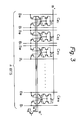
- Fig. 3 illustrates an array which forms n bits by using the memory cells illustrated in Figs. 1A and 2, which array provides a hold circuit.
- Ce 1 , Ce 2 , ... Ce n designate a first, a second, ... , an n'th cell, respectively.
- a common emitter n type conduction region of a column wire W- is used, as already mentioned, as an underpass connection.
- a transistor Q 7 is provided for supplying injection currents i l , i 2 , ... in to the cells Ce 1 , Ce 2 , ... , Ce n in the array, and the transistor Q 7 is used as the current source for supplying the hold current I H . Therefore, the following equation can be established.
- the common emitter n type region of the word line W- consists of two n type layers, an epitaxial layer and a burried layer.
- the epitaxial layer is formed on the burried layer which has higher density of the impurity than the epitaxial layer. Therefore, the word line W-has a larger resistance than a metalic layer, and this resistance is due to the bulk resistance and exists between each cell. This resistance deteriorates the characteristics of the semiconductor memory which utilizes integrated injection logic memory cells. This is due to the following reason.
- Fig. 4A As the cells Ce 1 ; Ce 2 , ... Ce n are illustrated as equivalent diodes which are connected between the word line W+ and the word line W-, the circuit illustrated in Fig. 3 can be illustrated as the equivalent circuit in Fig. 4A.
- "D" designates the equivalent diode
- R 0 designates a series resistance which is due to the afore-mentioned n type epitaxial layer
- “R H” designates a resistance component between the memory cells
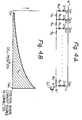
- the injection current supplied to each memory cell exponentially decreases from the cell Ce n to the cell Ce 1 as shown in Fig. 4B, due to the resistance R H , which exists in the word line W- between each cell. That is, the injection current which is supplied to the cell Ce 1 ), which is at an opposite end to the transistor Q 7 has a minimum value.
- the injection current which can assure the function of the memory cells has a lower limit which is determined by the current amplification factor h FE of the transistor. Further, as it is required that all memory cells in the memory array be assured, the hold current I H in the memory array must be determined taking into the consideration the minimum injection current supplied to the memory cell Ce l . Therefore, surplus injection currents must be supplied in the cell Ce 2 , ... , Ce n , and the excessive electrical power must be disipated in the memory array. Further, as the injection current to each cell is exponentially distributed, as shown in Fig. 4B, in accordance with the position of the cells, the read and write characteristics of the memory cells are also different in accordance with the position of the cells.
- Fig. 5 illustrates a circuit of one embodiment of the present invention.
- the circuit illustrated in Fig. 5 is formed as an n bits array and the same symbols as used in Fig. 3 indicate the same elements as in Fig. 3.
- the transistor Q 7 is connected to one end of the word line W-, at a position near the memory cell Ce n , and the current is supplied to the transistor Q 7 .
- a transistor Q 8 is connected to the other end of the word line W-, at a position near the memory cell Ce 1 , and the current is supplied to the transistor Q 8 . That is, in the present invention, the transistors Q 7 and Q 8 are connected respectively to each end of the word line W- and the hold current I H is equally distributed to the transistors Q 7 and Q 8 .
- a broken line Q 7 shows the distribution of the injection currents when only the transistor Q 7 is provided
- the borken line Q 8 shows the distribution of the injection currents when only the transistor Q 8 is provided.
- the value of the injection current has a maximum value at the side where the transistor is connected and the values of the injection current decrease exponentially.
- the distribution of the injection current which is shown by the full line Q 7 + Q8 can be obtained. That is, by the combination of the characteristics shown by the broken lines Q 7 and Q 8 , the injection current supplied to each cell can be equalized.
- Fig. 7A is a plan view of the essential part of the circuit illustrated in Fig. 5 and Fig. 7B illustrates a cross sectional view of the circuit near the transistor Q 8 in Fig. 7A.
- the dimensions of the word lines W+, W-, and "n" and "p" type diffusion regions are not proportional to the actual circuit.
- the word line W- that is, the common "n" type conduction region of the bulk, is commonly used in the collectors of the transistor Q 7 and Q 8 .
- the areas of emitters E 7 and E 8 of the transistors Q 7 and Q 8 are equal and each emitter of the transistors Q 7 and Q 8 is connected via a connection wire to a terminal V E .
- bases B 7 and B 8 of the transistors Q 7 and Q 8 are connected via a connection wire to a terminal V B .
- the scope of the present invention is not limitted to the above-mentioned embodiment, and many modifications thereof are possible.
- the "npn" type integrated injection memory is used in the memory cell, however, the present invention can be used regardless of the conduction type of the memory cell when the resistance exists in the word line (for example W-).
- the transistors used as the current source are provided at both ends of the word line, however, for the purpose of more uniformly distributing, the current source can be provided at the middle point of the word line, as illustrated in Fig. 8.
- Fig. 9 shows the distribution of the injection currents supplied to each cell in the circuit illustrated in Fig. 8.
- curves Q 7 , Q 8 , Q 9 respectively show the distribution of the injection current when only the transistor Q 7 , Q 8 or Q 9 is provided.
- a curve Q 7 + Q8 shows the distribution of the injection currents when the transistors Q 7 and Q 8 are connected to both ends of the word line, and this curve Q 7 + Q 8 corresponds to the full line Q 7 + Q 8 shown in Fig. 6.
- a flatter distribution curve Q 7 + Q 8 + Q 9 than that of Fig. 5 can be obtained.
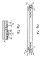
- Fig. 10A is a plan view of the essential part of the circuit illustrated in Fig. 8 and in Fig. 10A, the distribution ratio of the hold currents is selected to be 1:2:1.
- Fig. 10B is a cross sectional view of the circuit near the transistor Q 9 at the middle point of the word line in Fig. 10A.
- Figs. 10A and 10B, the dimensions of the word lines W+ and W-, and the "n" and "p" type diffusion regions is not proportional to the actual circuit.
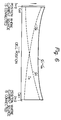
- Fig. 11A shows examples of the result of the simulation of the injection current to each Cell Ce 1 , Ce 2 , ... , Ce in the circuit illustrated in Fig. 8.
- Fig. 11A shows the variation of the distribution of the injection currents when the ratio of the hold current I 1 , I 2 and 1 3 in the equivalent circuit of Fig. 11B is changed.
- the value of the vertical axis is magnified in order to distinguish the differences between the cases.
- a designates a curve obtained when the ratio of the hold currents is selected to be 2:1:2,
- b designates a curve obtained when the ratio of the hold currents is selected to be 1:1:1,
- c designates a curve obtained when the ratio of the hold currents is selected to be 1:2:1, and
- d designates a curve when the ratio of the hold currents is selected to be 1:3:1.
- Figs. 11A and 11B it is assumed that the sum of the hold currents I 1 , 12 and 1 3 is constant and that the value of the resistance R H is in the range of from 20 to 100 ⁇ . As illustrated in Fig.
- the flattest distribution curve of the injection currents of the cells can be obtained when the dividing ratio of the hold current I H is selected to be 1:2:1.
- the embodiment illustrated in Fig. 10A is based on this flattest distribution curve. Further, a flatter distribution curve can be obtained by providing further current sources and by selecting a suitable ratio of the hold currents.
- the semiconductor bulk is used as the word line, however, it should be understood that the the semiconductor bulk can be used as the bit line.
- the distribution of the injection currents to each cell can be equalized by providing current sources at both ends of the memory cell array or by further providing a current source at a middle portion of the memory cell array. Therefore, the surplus current which flows in each memory cell can be removed so that no excessive power of the memory cell array is dissipated. Further, the value of a minimum injection current to each cell can be increased as compared with the conventional memory cell array, so that the design margin of the action of the memory cell array can be increased. In additoin, as the injection current to each cell is not influenced by the position of the cell, the write and read characteristics of the memory cells can be equalized.
Landscapes
- Engineering & Computer Science (AREA)
- Microelectronics & Electronic Packaging (AREA)
- Computer Hardware Design (AREA)
- Static Random-Access Memory (AREA)
- Semiconductor Memories (AREA)
- Internal Circuitry In Semiconductor Integrated Circuit Devices (AREA)
- Semiconductor Integrated Circuits (AREA)
- Bipolar Integrated Circuits (AREA)
Applications Claiming Priority (2)
| Application Number | Priority Date | Filing Date | Title |
|---|---|---|---|
| JP53071666A JPS5826179B2 (ja) | 1978-06-14 | 1978-06-14 | 半導体集積回路装置 |
| JP71666/78 | 1978-06-14 |
Publications (2)
| Publication Number | Publication Date |
|---|---|
| EP0006702A1 true EP0006702A1 (fr) | 1980-01-09 |
| EP0006702B1 EP0006702B1 (fr) | 1982-01-27 |
Family
ID=13467142
Family Applications (1)
| Application Number | Title | Priority Date | Filing Date |
|---|---|---|---|
| EP79301092A Expired EP0006702B1 (fr) | 1978-06-14 | 1979-06-08 | Circuit intégré semiconducteur à mémoire |
Country Status (4)
| Country | Link |
|---|---|
| US (1) | US4231108A (fr) |
| EP (1) | EP0006702B1 (fr) |
| JP (1) | JPS5826179B2 (fr) |
| DE (1) | DE2961954D1 (fr) |
Cited By (2)
| Publication number | Priority date | Publication date | Assignee | Title |
|---|---|---|---|---|
| EP0028306A1 (fr) * | 1979-11-02 | 1981-05-13 | International Business Machines Corporation | Dispositif de mémoire à semi-conducteurs à cellules de mémoire du type I2L |
| EP0454061A3 (en) * | 1990-04-27 | 1993-01-27 | Nec Corporation | Dynamic random access memory device with improved power supply system for speed-up of rewriting operation on data bits read-out from memory cells |
Families Citing this family (7)
| Publication number | Priority date | Publication date | Assignee | Title |
|---|---|---|---|---|
| JPS5842556B2 (ja) * | 1979-08-30 | 1983-09-20 | 富士通株式会社 | 半導体記憶装置 |
| US9190144B2 (en) | 2012-10-12 | 2015-11-17 | Micron Technology, Inc. | Memory device architecture |
| US8891280B2 (en) | 2012-10-12 | 2014-11-18 | Micron Technology, Inc. | Interconnection for memory electrodes |
| US9025398B2 (en) | 2012-10-12 | 2015-05-05 | Micron Technology, Inc. | Metallization scheme for integrated circuit |
| US9224635B2 (en) | 2013-02-26 | 2015-12-29 | Micron Technology, Inc. | Connections for memory electrode lines |
| US10074693B2 (en) | 2015-03-03 | 2018-09-11 | Micron Technology, Inc | Connections for memory electrode lines |
| JP6708158B2 (ja) | 2017-04-14 | 2020-06-10 | 信越化学工業株式会社 | 粘着剤組成物およびこの組成物を用いてなるフィルム |
Citations (2)
| Publication number | Priority date | Publication date | Assignee | Title |
|---|---|---|---|---|
| US3815106A (en) * | 1972-05-11 | 1974-06-04 | S Wiedmann | Flip-flop memory cell arrangement |
| FR2338546A1 (fr) * | 1976-01-15 | 1977-08-12 | Itt | Cellule de memoire bipolaire en logique a injection integree a injecteurs lateraux et verticaux |
Family Cites Families (1)
| Publication number | Priority date | Publication date | Assignee | Title |
|---|---|---|---|---|
| US3959781A (en) * | 1974-11-04 | 1976-05-25 | Intel Corporation | Semiconductor random access memory |
-
1978
- 1978-06-14 JP JP53071666A patent/JPS5826179B2/ja not_active Expired
-
1979
- 1979-06-08 EP EP79301092A patent/EP0006702B1/fr not_active Expired
- 1979-06-08 DE DE7979301092T patent/DE2961954D1/de not_active Expired
- 1979-06-13 US US06/048,256 patent/US4231108A/en not_active Expired - Lifetime
Patent Citations (3)
| Publication number | Priority date | Publication date | Assignee | Title |
|---|---|---|---|---|
| US3815106A (en) * | 1972-05-11 | 1974-06-04 | S Wiedmann | Flip-flop memory cell arrangement |
| FR2338546A1 (fr) * | 1976-01-15 | 1977-08-12 | Itt | Cellule de memoire bipolaire en logique a injection integree a injecteurs lateraux et verticaux |
| US4144586A (en) * | 1976-01-15 | 1979-03-13 | International Telephone & Telegraph Corp. | Substrate-fed injection-coupled memory |
Non-Patent Citations (1)
| Title |
|---|
| IBM TECHNICAL DISCLOSURE BULLETIN, Vol. 18, March 1976, New York M.A. BATTISTA et al. "Lateral pnp structure for memory cell" pages 3254-3255. * Pages 3254-3255 * * |
Cited By (2)
| Publication number | Priority date | Publication date | Assignee | Title |
|---|---|---|---|---|
| EP0028306A1 (fr) * | 1979-11-02 | 1981-05-13 | International Business Machines Corporation | Dispositif de mémoire à semi-conducteurs à cellules de mémoire du type I2L |
| EP0454061A3 (en) * | 1990-04-27 | 1993-01-27 | Nec Corporation | Dynamic random access memory device with improved power supply system for speed-up of rewriting operation on data bits read-out from memory cells |
Also Published As
| Publication number | Publication date |
|---|---|
| DE2961954D1 (en) | 1982-03-11 |
| JPS54162981A (en) | 1979-12-25 |
| EP0006702B1 (fr) | 1982-01-27 |
| US4231108A (en) | 1980-10-28 |
| JPS5826179B2 (ja) | 1983-06-01 |
Similar Documents
| Publication | Publication Date | Title |
|---|---|---|
| EP0008946B1 (fr) | Dispositif de mémoire à semi-conducteur | |
| EP0090665B1 (fr) | Dispositif semi-conducteur à mémoire | |
| US3643235A (en) | Monolithic semiconductor memory | |
| US4480319A (en) | Emitter coupled flip flop memory with complementary bipolar loads | |
| US4021786A (en) | Memory cell circuit and semiconductor structure therefore | |
| CA1152646A (fr) | Cellule de memoire pour memoire statique et memoire statique comprenant une telle cellule | |
| EP0006702B1 (fr) | Circuit intégré semiconducteur à mémoire | |
| US4419745A (en) | Semiconductor memory device | |
| EP0005601B1 (fr) | Circuit semiconducteur intégré à mémoire | |
| US5065216A (en) | Semiconductor integrated circuit having interconnection with improved design flexibility, and method of production | |
| EP0028157B1 (fr) | Circuit intégré semiconducteur à mémoire à logique d'injection intégrée | |
| US4231109A (en) | Semiconductor integrated circuit device | |
| EP0078222A2 (fr) | Cellule de mémoire bipolaire à circuit intégré | |
| US4812891A (en) | Bipolar lateral pass-transistor for CMOS circuits | |
| US4069428A (en) | Transistor-transistor-logic circuit | |
| US4388636A (en) | Static memory cell and memory constructed from such cells | |
| EP0084000A2 (fr) | Dispositif CMOS | |
| US4622575A (en) | Integrated circuit bipolar memory cell | |
| US4170017A (en) | Highly integrated semiconductor structure providing a diode-resistor circuit configuration | |
| US3725881A (en) | Two terminal bipolar memory cell | |
| US4656495A (en) | Bipolar ram cell and process | |
| EP0182718B1 (fr) | Dispositif de mémoire semi-conductrice | |
| US5014243A (en) | Programmable read only memory (PROM) having circular shaped emitter regions | |
| CA1259135A (fr) | Memoire a acces selectif a charge active | |
| JPH061819B2 (ja) | 半導体記憶装置 |
Legal Events
| Date | Code | Title | Description |
|---|---|---|---|
| PUAI | Public reference made under article 153(3) epc to a published international application that has entered the european phase |
Free format text: ORIGINAL CODE: 0009012 |
|
| AK | Designated contracting states |
Designated state(s): DE GB NL |
|
| 17P | Request for examination filed | ||
| GRAA | (expected) grant |
Free format text: ORIGINAL CODE: 0009210 |
|
| AK | Designated contracting states |
Designated state(s): DE GB NL |
|
| REF | Corresponds to: |
Ref document number: 2961954 Country of ref document: DE Date of ref document: 19820311 |
|
| REG | Reference to a national code |
Ref country code: GB Ref legal event code: 732 |
|
| NLS | Nl: assignments of ep-patents |
Owner name: NIPPON TELEGRAPH AND TELEPHONE CORPORATION TE TOKI |
|
| PGFP | Annual fee paid to national office [announced via postgrant information from national office to epo] |
Ref country code: GB Payment date: 19980601 Year of fee payment: 20 |
|
| PGFP | Annual fee paid to national office [announced via postgrant information from national office to epo] |
Ref country code: DE Payment date: 19980612 Year of fee payment: 20 |
|
| PGFP | Annual fee paid to national office [announced via postgrant information from national office to epo] |
Ref country code: NL Payment date: 19980629 Year of fee payment: 20 |
|
| PG25 | Lapsed in a contracting state [announced via postgrant information from national office to epo] |
Ref country code: GB Free format text: LAPSE BECAUSE OF NON-PAYMENT OF DUE FEES Effective date: 19990607 |
|
| PG25 | Lapsed in a contracting state [announced via postgrant information from national office to epo] |
Ref country code: NL Free format text: LAPSE BECAUSE OF EXPIRATION OF PROTECTION Effective date: 19990608 |
|
| REG | Reference to a national code |
Ref country code: GB Ref legal event code: PE20 Effective date: 19990607 |
|
| NLV7 | Nl: ceased due to reaching the maximum lifetime of a patent |
Effective date: 19990608 |
|
| PLBE | No opposition filed within time limit |
Free format text: ORIGINAL CODE: 0009261 |
|
| STAA | Information on the status of an ep patent application or granted ep patent |
Free format text: STATUS: NO OPPOSITION FILED WITHIN TIME LIMIT |