EP0015548A2 - Procédé et appareil pour juger d'un revêtement par traitement non électrique - Google Patents
Procédé et appareil pour juger d'un revêtement par traitement non électrique Download PDFInfo
- Publication number
- EP0015548A2 EP0015548A2 EP80101116A EP80101116A EP0015548A2 EP 0015548 A2 EP0015548 A2 EP 0015548A2 EP 80101116 A EP80101116 A EP 80101116A EP 80101116 A EP80101116 A EP 80101116A EP 0015548 A2 EP0015548 A2 EP 0015548A2
- Authority
- EP
- European Patent Office
- Prior art keywords
- test piece
- potential
- elp
- charge
- polarization potential
- Prior art date
- Legal status (The legal status is an assumption and is not a legal conclusion. Google has not performed a legal analysis and makes no representation as to the accuracy of the status listed.)
- Granted
Links
Images


Classifications
-
- G—PHYSICS
- G01—MEASURING; TESTING
- G01N—INVESTIGATING OR ANALYSING MATERIALS BY DETERMINING THEIR CHEMICAL OR PHYSICAL PROPERTIES
- G01N17/00—Investigating resistance of materials to the weather, to corrosion, or to light
- G01N17/02—Electrochemical measuring systems for weathering, corrosion or corrosion-protection measurement
Definitions
- This invention relates to a method and apparatus for evaluating electroless plating, more specifically the rate of electroless plating, the weight of a metal layer formed by the plating (or thickness thereof), the surface condition of the metal layer, the chemical composition of a plating bath used, the adhesion of the metal film, and so forth.
- the invention relates to a method and apparatus for detecting the speed of electroless plating, using coulostatic method.
- Methods which detect the rate of electroless plating or chemical plating. Methods for measuring the thickness of a metal film formed by such plating are also known. Further, various methods for detecting the chemical property of a plating bath are known.
- a micrometer is used to measure the thickness of a metal layer formed by electroless plating or chemical plating.
- a metal layer weight formed by electroless plating is obtained based on the difference between the weight of a substrate before the plating and the weight of the substrate after the plating. With both methods it takes a long time to detect the thickness of a metal layer. Further, with these methods it is difficult to measure other factor of electroless plating, such as the change of rate of plating.
- a method which detects pH, temperature and metal ion concentration of a plating bath.
- it is difficult with this method to detect an accurate rate of plating.
- the method is therefore not effective in controlling the chemical property of a plating bath.
- This method does not directly measure the plating rate, and the measured potential is affected by other factors. In some cases it is difficult with the method to estimate the plating rate accurately.
- Izumi Ohno "kinzoku Hyomen Gijutsu", 29, 600, 1978 discloses a method for estimating a plating rate.
- a slight polarization is caused on a metal test piece immersed in a plating bath, and a deposition resistance R ELP of the test piece is obtained based on the relationship between the polarization potential of the test piece and the current.
- current must flow through the test piece for a relatively long time. This would destroy the natural plating condition.
- the reaction resistance is not sufficiently large to neglect the solution resistance of the plating bath. The solution resistance of the plating bath, can not therefore be negligible in comparison with the reaction resistance and will probably lead to estimate an incorrect plating rate.
- An object of this invention is to provide a method and apparatus for evaluating electroless plating, both accurately and quickly.
- This invention provides a method of evaluating electroless plating, comprising a step of determining the reaction resistance R ELP of a test piece having a surface area S and disposed in a electroless plating bath, said step comprising:
- This invention further provides an apparatus for evaluating the electroless plating comprising:
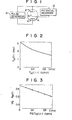
- a method of measuring the rate of electroless plating according to this invention is an application of coulostatic method, wherein the rate of electroless plating is analyzed based on the measurements obtained by such a measuring apparatus as illustrated in Fig. 1.
- the interface between an electrode and a solution acts as a leaky capacitor.
- An electrical double layer at the interface is instantaneously charged with a given amount of charge.
- the process of consuming the given charge by the electrode reaction is recorded as a variation of electrode potential with respect to time.
- the rate of the electrode reaction is calculated based on the recorded data.
- the measuring apparatus'shown in Fig. 1 is designed to detect how the polarization potential n R (t) and time t is recorded by a potential recorder 12 three times under different conditions, thereby obtaining the three n R (t)-t curves.
- the n R (t)-t curves are analyzed to obtain the reaction resistance R ELP of the test piece 2, a Tafel slope ⁇ a of anodic reaction and a Tafel slope ⁇ c of cathodic reaction, respectively.
- an electroless plating current density I ELP is calculated by the following formula: where
- M denotes the atomic weight of metal deposited on the test piece 2
- n the valence of the deposited metal ion
- F the Faraday constant
- the quantity of charges Q ELP consumed by the plating is expressed by the following formula: Further, the weight W ELP of metal deposited is expressed by the following formula:
- W ELP is of course weight of metal per unit surface area of the test piece 2, whose surface area is S.
- the thickness d ELP of the metal film deposited on the test piece 2 can therefore be obtained by the following formula:
- Equation (5) denotes the specific gravity of the metal deposited on the test piece 2.
- the surface area S of the test piece 2 is measured, and the test piece 2 is put into a cell 4 filled with a plating bath.
- the test piece 2 functions as a working electrode.
- it is a piece of metal to be plated. It may be a piece of nonmetallic material, e.g. plastics.
- an electrode terminal (not shown) is attached to the test piece 2 so that is may be electrically connected to a metal layer to be deposited on the test piece 2. In this case, the metal layer deposited on the test piece 2 functions as a working electrode.
- a counter electrode 6 is disposed in the cell 4. Between the test piece 2 and the counter electrode 6 a reference electrode 8 is arranged.
- the reference electrode 8 is made of copper (Cu), nickel (Ni), platinum (Pt), palladium (Pd), chromium (Cr), rhodium (Rh), iridium (Ir) or the like. Preferably, it is made of the same material as the test piece 2. If the electrodes 8 and the test piece 2 are made of the same material, their natural potentials, i.e. electroless deposition potentials E ELP are substantially equal, thus rendering it unnecessary to apply a bias voltage to cancel their natural potentials.
- the counter electrode 6 is made of copper (Cu), nickel (Ni), platinum (Pt), palladium (Pd) or the like. These electrodes 2, 6 and 8 may be shaped in various ways. For example, they are shaped like rods or plates.
- a pulse generator 10 to apply a predetermined charge.
- a potential recorder 12 to detect the polarization potential ⁇ R (t) of the test piece 2.
- the recorder 12 has a high input impedance.
- the potential recorder 12 records three n R (t)-t curves under different conditions, so that the reaction resistance R ELP , anodic Tafel slope ⁇ a and cathodic Tafel slope B c may be obtained.
- a first n R (t)-t curve is analyzed to obtain the reaction resistance R EL p, a second n R (t)-t curve to obtain anodic Tafel slope B a , and the third n R (t)-t curve to obtain cathodic Tafel slope B c .
- reaction resistance R ELP Via the counter electrode 6 a predetermined charge q R is applied to the test piece 2 for such a short time as several microseconds to a few milliseconds, thus charging instantaneously the electrical double layer of the test piece 2.
- the charge q R is of such a positive value or negative value as to arise the polarization potential n R (t) of the test piece 2 by not more than 30 millivolts, preferably by 10 millivolts or less.
- the charge q R on the electrical double layer is consumed by an electroless plating reaction of the test piece 2.
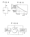
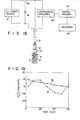
- the potential n R (t) of the test piece 2 varies with time to the natural potential, electroless deposition potential E EL p. This potential variation is detected by using the reference electrode 8 and recorded by the potential recorder 12, thereby obtaining such n R (t)-t curve as shown in Fig..2 and also such log ⁇ R (t)-t curve as shown in Fig. 3.
- the potential recorder 12 Since the potential recorder 12 has a high input impedance, the current flowing from the test piece 2 ti the recorder 12 via the reference electrode 8 can be neglected.
- the polarization potential n R (t) of the test piece 2 can therefore be considered to be measured by an open circuit, and the decay of the polarization potential n R (t) can be regarded as having been caused by the electroless plating reaction of the test piece 2 alone.
- n R (t)-t curve illustrated in Fig. 2 is analyzed to obtain the reaction resistance R ELP of the test piece 2 in the following manner.
- the potential of the test piece 2 in the plating bath is first at the electroless deposition potential E ELP .
- E ELP electroless deposition potential
- the initial polarization potential n R (0) of the test piece 2 is then expressed as follows:
- the initial polarization potential n R (0) cannot be measured directly by the potential recorder 12 because the ohmic drop of the resistance R s of the test plating bath gives incorrect measurement.
- the variation of the polarization potential n R (t) with respect to time recorded by the recorder 12 is theoretically given by the following formula:
- Equation (7) may be transformed into the following logarithmic equation:
- C D is the differential capacitance of the test piece 2.
- the values of both C D and R EL p are given per unit surface area of the test piece 2.
- the differential capacitance C D may be expressed as follows:
- ⁇ q R q R/ S.
- q R denotes a charge
- S denotes the surface area of the test piece 2.
- the differential capacitance C D varies depending on the potential of the test piece 2. But it is considered substantially constant within a small potential domain.
- the reaction resistance R ELP is calculated from the data recorded by the recorder 12 and by equations (8) and (9).
- Equation (8) represents a rectilinear line and the log n R (t)-t curve is linearly plotted on a semi- logarithmic graph shown in Fig. 3.
- the differential capacitance C D is obtained by substituting the initial polarization potential n R (0) into equation (9). Based on the slope of the rectilinear line in Fig. 3 and the differential capacitance C D the reaction resistance R ELP can be therefore obtained.
- the electroless plating reaction of the test piece 2 in the plating bath may be electrically represented in the form of such an equivalent circuit shown in Fig. 4.
- the resistance R s of the plating bath serves as a resistor to the electric current which flows when the differential capacitance C D is charged up.
- the polarization potential n R (t) is detected by substantially an open circuit.
- the measured value of the reaction resistance R ELP is therefore never affected by the bath resistance R s . If the measured value of the resistance R EL p is affected slightly by the bath resistance R s , the initial polarization potential n R (0) can be obtained correctly by extrapolation. If the equivalent circuit of Fig.
- the electroless plating reaction can be electrically detected in the form of a transient phenomenon in a closed circuit consisting of the capacitor C D and the resistor R ELP . That is, the electroless plating reaction can be said to be a phenomenon in which the charge density ⁇ q R of the charged capacitor C D is consumed in the resistor R ELP ⁇
- electroless plating is known as a kind of electrochemical reaction, a combination of the anodic oxidation of a reducing agent and the cathodic reduction of metal ion. That is, the electroless plating is believed to take place when the anodic oxidation (Red ⁇ Ox + ne) of a reducing agent and the cathodic reduction (M n+ + ne ⁇ M) of metal ion proceed at the same time, with the same current and thus developing at the same speed.
- the current during the electroless plating is called “electroless deposition current density I EL p", and the potential built up during the plating is called “electroless deposition potential E ELP ".
- the potential is elevated from the electroless deposition potential E ELP , such relationship as expressed by the following equation (10) will be established between the polarization potential n(t) and the external current I(t), i.e. Faradaic current density:
- equation (10) represents electroless plating reaction.
- R denotes gas constant
- T the absolute temperature
- ⁇ a 2.3 ⁇ RT/ a nF
- ⁇ c 2.3 ⁇ RT/ ⁇ c nF.
- equation (1) can be transformed into the following equation:
- Equation (7) is derived from equation (11) in the following manner.
- the charge density ⁇ q R consumed by the electroless plating reaction from time 0 to time t can be expressed as follows:
- the polarization resistance R ELP can be calculated based on the slope of the rectilinear line in Fig. 3 and the differential capacitance C D , which has been calculated based on the charge density ⁇ q R and the initial polarization potential ⁇ R (0).
- the second ⁇ ⁇ a (t)-t curve from which to obtain anodic Tafel slope S a .
- a predetermined charge q ⁇ a is applied to the test piece 2 for a short time for example, several microseconds to a few milliseconds, thus charging instantaneously the electrical double layer of the test piece 2.
- the charge q ⁇ a is larger than the charge q R applied to the test piece in order to obtain the reaction resistance R ELP . More specifically, the charge q ⁇ a is of such a value as to elevate the polarization potential n Sa (t) of the test piece 2 to 30 millivolts or more, preferably to 50 millivolts or more.
- the charge q ⁇ a is used up by the electroless reaction of the test piece 2, and the potential of the test piece 2 gradually varies with time. This potential variation is detected by using the reference electrode 8 and recorded by the potential recorder 12, thereby obtaining such a ⁇ ⁇ a (t)-t curve shown in Fig. 5.
- the third ⁇ ⁇ c (t)-t curve from which to obtain cathodic Tafel slope ⁇ c is recorded.
- a predetermined charge q ⁇ c of the opposite polarity to the charge q ⁇ c is applied through the counter electrode 6 to the test metal piece for such a short time as several microseconds to a few milli seconds.
- the charge qs c is of such a value as to lower the polarization potential ⁇ ⁇ c (t) of the test piece 2 to tens of minus millivolts, preferably to -50 millivolts or less.
- the three ⁇ ⁇ a (t)-t curves need not be obtained in the above-mentioned order. But it is desired that a charge should not be applied to the test piece 2 until the potential of the test metal 2 returns to the natural potential, i.e. electroless deposition potential E ELP . To bring the potential of the test piece 2 quickly back to the electroless deposition potential E EL p, a backward bias may be applied to the test piece 2.
- charge q ⁇ a which satisfies equation (17), is applied to the test piece 2 at the electroless deposition potential E ELP and that the polarization potential of the test piece 2 arises to n m . Then, the polarization potential varies as time elapses.
- a specific polarization potential ni is selected, which is represented as: 0 ⁇ i ⁇ m .
- the time count is started again. If the differential capacitance C D remains constant over the period of time t in which the polarization potential varies from ni to n sa (t), then the charge consumed during the period ⁇ q ⁇ a can be represented as follows:
- Faradaic current density I in equation (17) corresponds to the current which has flown during the electroless plating reaction.
- this current I is integrated over time t, the consumed charge q a is equal to the integrated value of the current I. That is:
- Equations (18) and (19) are differentiated into the following equation:
- Equation (27) shows that Tafel Slope ⁇ a of anodic reaction can be obtained if the polarization potential ⁇ ⁇ a (t 1 ), ⁇ ⁇ a (t 2 ) and ⁇ ⁇ a (t 3 ) at three different times t l , t 2 and t 3 are read.
- Equation (28) shows that anodic Tafel slope ⁇ a can be easily calculated by reading from the ⁇ ⁇ a (t)-t curve ⁇ ⁇ a (t)>>0 the time t 2 at which the potential ⁇ ⁇ a (t 2 ) is recorded, the time t 1 at which the potential ⁇ ⁇ a (t 1 ) higher than ⁇ ⁇ a (t 2 ) by ⁇ ⁇ a is recorded and the time t 3 at which the potential ⁇ ⁇ a (t 3 ) lower than ⁇ ⁇ a (t 2 ) by ⁇ ⁇ a is recorded.
- Tafel slope ⁇ a is calculated based on only ⁇ ⁇ a , t l , t 2 and t 3 .
- Tafel slope ⁇ a is calculated accurately in the following way.
- ⁇ ⁇ a (t)-t curve as shown in Fig. 5 is obtained, wherein ⁇ ⁇ a (t) is more than 50 millivolts.
- Equation (28) is rewritten into the following equation using the average ⁇ ;
- the polarization potential ⁇ ⁇ c (t) is changed to not more than -30 millivolts, preferably -60 to -50 millivolts or lower. Then the following equation will be established:
- Equation (31) is similar to equation (17). Thus, similar equations to equations (18), (19) and (20) are established. And the following equation, which is similar to equation (21), is also established:
- cathodic Tafel slope ⁇ c is expressed as follows:
- the quantity of electricity Q ELP consumed by the electroless plating is obtained as expressed by equation (3). Further, the weight W ELP of metal deposited is obtained as shown in equation (4).
- the surface condition of the metal layer deposited and the condition of the plating bath can be evaluated in accordance with a variation of the differential capacitance C D as shown in equation (9). Further, the adhesion of the metal layer deposited on the metal piece 2 can be evaluated according to a variation of the reaction resistance R EL p which is read from the log n R (t)-t curve which in turn is obtained from equation (8).
- Tafel slopes S a and ⁇ c may be regarded as constants, and the rate of plating V EL p may be obtained based only on the reaction resistance R ELP .
- the apparatus shown in Fig. 1 is a three-electrode type. It has three electrodes, i.e. the test piece 2 (working electrode), the counter electrode 6 and the reference electrode 8. This three-electrode type apparatus may be replaced by such a two-electrode type as illustrated in Fig. 6.
- the apparatus shown in Fig. 6 comprises a test piece (or working electrode) 2 and a reference electrode 8 which acts as a counter electrode for supplying charge to the test piece 2, too.
- the reference electrode 8 functions to detect the polarization potential of the test piece 2.
- the reference electrode 8 should keep its potential constant during measurement.
- a pulse generator 10 and a potential recorder 12 are connected as shown in Fig. 6.
- test piece 2 and the electrode 8 of the apparatus shown in Fig. 6 are made of the same material, electroless plating reaction takes place on the reference electrode 8 in the same manner as the test piece 2.
- the potential recorder 12 detects the difference in polarization potential between the test piece 2 and the reference electrode 8.
- S 1 denotes the area of the first test metal piece 2
- S 2 the area of the second test metal piece 8.
- Equation (36) is formulated in the following way.
- the charge q l between the solution and the electrical double layer of the first test piece 2 has the opposite polarity to the charge q 2 between the solution and the electrical double layer of the second test piece 8. Both charge q 1 and q 2 are of the same absolute value.
- the surface charge density ⁇ q 1 of the first piece 2 and the surface charge density Aq 2 of the second piece 64 are represented by the following equations (37) and (38), respectively:
- ⁇ 1 (0) denotes the initial polarization potential of the first test piece 2
- ⁇ 2 (0) the initial polarization potential of the second test piece 8.
- these initial polarization potentials can be represented by the following equations:
- equations (38) and (39) are transformed as follows:
- equation (43) is transformed into equation (36):
- differential capacitance C D can easily be obtained by equation (36) or (44), just as easily as by equation (9).
- the electrodes of the apparatus should better be arranged as shown in Fig. 7.
- An electroless plating bath is generally stirred by means of an air blower so that it is made stable enough to form a metal layer of a uniform thickness.
- the plating bath is stirred, however, it flows along unsteady courses. Such random flow of liquid would in some case create noise in the measured potential.
- th test piece 2 and the reference electrode 8 are connected to the potential recorder 12 by wires. If these wires are not electrically shielded, the noise is likely to sneak into the measured potential through the wires. The noise thus reduce the accuracy of the measurement.
- a hollow cylinder which is made of a net or which has many apertures is used as a counter electrode 6, and the test piece 2 and the reference electrode 8 are disposed within the counter electrode 6.
- the counter electrode 6 protects the test piece 2 and the electrode 8 against a random flow of plating bath.
- wires 13 which connect the test piece 2, the counter electrode 6 and the reference electrode 8 to the pulse generator 10 and the potential recorder 12 extend through a shield sheath 15, which is attached to a shield case 17 shielding the pulse generator 10 and the potential difference recorder 12.
- test piece 2 and the reference electrode 8 are disposed in the hollow cylindrical counter electrode 6, the noise created by the stirring of the plating bath and that induced by AC lines are prohibited from reaching the test piece 2 and the reference electrode 8. Further, since the wires 13 are protected by the shield sheath 15, the noise is prevented from reaching the potential difference recorder 12. As a result, the accuracy of measurement will be enhanced.
- the hollow cylindrical counter electrode 6 may be disposed within a hollow cylindrical shield electrode 19 which is made of a net or which has many apertures, as illustrated in Fig. 8. It is preferred that the shield electrode 19 should be connected to the shield sheath 15. It is also preferred that the shield electrode 19 should be made of the same material as the counter electrode 6. Of course, it is sufficient if the electrodes 6 and 19 are made of such material as is electrically conductive and as would not emit ions in the plating bath to impede the electroless plating reaction. Further, the shield electrode 19 may be coated with a resin, glass or the like so that a metal may not be deposited on it.
- the apparatus shown in Fig. 9 comprises a metal test piece 2, a cell 4 filled with test liquid, a counter electrode 6, a reference electrode 8, a pulse generator 10 and a potential recorder 12.
- the potential recorder 12 may include a bias voltage source (not shown) which applies a bias voltage to the detected potential, thereby to detect only the variation of polarization potential n(t). In other words, the bias voltage source cancells out the electroless deposition potential from the output signal of the potential recorder 12.
- the pulse generator 10 is constituted by a power source 16, four capacitors 18-1 to 18-4 for accumulating charge from the power source 16, a rotary switch 20 for selecting one of the capacitors and a first switching circuit 22 for instantaneously applying charge from the selected capacitor to the metal test piece 2.
- the capacitors 18-1 to 18-4 have different capacitances C l to C 4 , respectively.
- One end of each capacitors is connected to the corresponding fixed contact of the rotary switch 20, and the other end to the power source 16 and the counter electrode 6.
- the movable contact of the switch 20 is connected to the power source 16 through the first switching circuit 22.
- the capacitors 18-1 to 18-4 and the rotary switch 20 constitute a series circuit.
- the pulse generator 10 is provided with a voltage measuring unit 25.
- the voltage measuring unit 25 is comprised of an operational amplifier 24 and a voltmeter 26, which are connected in series. This unit 25 is connected in parallel to the series circuit of the capacitors 18-1 to 18-4 and the rotary switch 20.
- the first switching circuit 22 connects the selected capacitor to the power source 16 so that the capacitor is charged. It connects any one of the capacitors 18-1 to 18-4 between the metal test piece 2 and the counter electrode 6 so that the electrical double layer of the test piece 2 is charged. As will be described later, the first switching circuit 22 is constituted by a timer and a relay.
- the measuring apparatus of Fig. 9 further comprises a second switching circuit 28 and a third switching circuit 30.
- the second switching circuit 28 is connected between the test piece 2 and the first switching circuit 22.
- the second switching circuit 28 disconnects the test piece 2 from the first switching circuit 22 upon completion of the necessary charge supply from the selected capacitor to the test piece 2 through the first switching circuit 22.
- the second switching circuit 28 is provided for detecting an accurated polarization potential of the test piece 2. That is, without the circuit 28, the selected capacitor would keep applying charge to the test piece 2 even while the recorder 12 is detecting the polarization potential of the test piece 2. As result, the recorder 12 would unnecessarily detect an ohmic drop. If the detected potential of the test piece 2 contains an ohmic drop, it is impossible to obtain a correct n(t)-t curve.
- the second switching circuit 28 opens upon lapse of a specific period of time from the start of charge supply to the test piece 2, thereby stopping the charge supply.
- the reference electrode 8 can detect exclusively the varying potential n(t) of the test piece 2, never an ohmic drop after the circuit 28 has opened. Consequently, a correct n(t)-t curve containing no error due to the solution resistance R s etc. is obtained.
- Said specific period is so long as to apply charge the test piece 2 to the predetermined polarization potential n(t) of -30 to 30 millivolts, preferably -10 to 10 millivolts, in order to obtain the reaction resistance R ELP , which is 30 millivolts or more, preferably 50 millivolts or more in order to obtain Tafel slope S a and which is -30 millivolts or less, preferably -50 millivolts or less in order to obtain Tafel slope S c . If the solution resistance R s is not so high, the second switching circuit 28 is unnecessary.
- the third switching circuit 30 is required particularly when one of the capacitors 18-1 to 18-4 which is connected to the test piece 2 and the counter electrode 6 can be charged to a voltage higher than the maximum voltage which the potential recorder 12 can measure. Thus, the third switching circuit 30 is unnecessary if the potential recorder 12 can measure a sufficiently high voltage.
- a data analyzing unit 32 is connected to the potential recorder 12 .
- the data analyzing unit 32 analyzes the charge q R applied to the test piece 2, initial polarization potential n(0) and differential capacitance C D in accordance with the capacitance of the selected capacitor, the potential change of the selected capacitor which has been detected by the voltmeter 26 and the change of polarization potential n(t) which has been detected by the recorder 12.
- the unit 32 calculates the reaction resistance R ELP and Tafel slopes ⁇ a and ⁇ c . Further it calculates the electroless plating current density I ELP .
- the unit 32 is connected to an integrating circuit 33.
- the integrating circuit 33 integrates the electroless plating current density I ELP , using a time parameter, thus obtaining the weight W ELP of the metal deposited on the test piece 2.
- a display unit 34 which can display the initial polarization potential n(0), the differential capacitance C D , the reaction resistance R ELP , Tafel slopes ⁇ a and B c , the electroless plating current density I ELP , plating weight W ELP , plating rate V ELP and so on.
- a synchroscope 35 is connected to the potential recorder 12. The synchroscope 35 can monitor the curve which shows the relationship between time and the polarization potential n(t) measured by the recorder 12.
- the measuring apparatus shown in Fig. 10 differs from the apparatus of Fig. 9 only in that a single switching circuit 37 is provided in place of the first switching circuit 22 and the second switching circuit 28.
- the switching circuit 37 connects the selected capacitor to the power source 16 so that the capacitor is charged. It connects the selected capacitor between the test piece 2 and the counter electrode 6 so that the charge is applied from the capacitor to the test piece 2. It disconnect the selected capacitor from the test piece 2 while the polarization potential of the test piece 2 is detected.
- the measuring apparatus shown in Fig. 9 is more fully illustrated in Fig. 11.
- the power source 16 is constituted by a battery 39, a pair of polarity changeover switches 36 and 38 ganged to each other, a variable resistor 40 and a switch 42.
- the variable resistor 40 and the switch 42 form a series circuit, which is connected between the movable contacts of the polarity changeover switches 36 and 38.
- the polarity changeover switches 36 and 38 are so connected to the battery 39 as to apply a positive charge or a negative charge to the test piece 2, thereby obtaining Tafel slope S a of the anodic reaction of the test piece 2 and Tafel slope S c of cathodic reaction of the test piece 2 and also obtaining reaction resistance R ELP , if necessary.
- the variable resistor 40 is provided to control the voltage applied to the selected capacitor.
- the first switching circuit 22 is constituted by a relay 44, a resistor 46, a battery 48 and a starting switch 50 for energizing the relay 44.
- the relay 44 has a first fixed contact connected to the movable contact of the variable resistor 40, a second fixed contact is connected to the test piece through the second switching circuit 28 and a movable contact connected to the rotary switch 20.
- the movable contact of the relay 44 is nor- 'mally in contact with the first fixed contact and is brought into contact with the second fixed contact when the relay 44 is energized.
- the second switching circuit 28 is constituted by a relay 54, a start switch 52 connected to the relay 54, a capacitor 56 connected in parallel to the series connected starting switch 52, and a resistor 58, and a battery 60.
- the relay 54 has a normally closed contact connected between the test piece 2 and the second fixed contact of the relay 44.
- the start switch 52 is ganged with the start switch 50 of the first switching circuit 22.
- the third switching circuit 30, which is connected between the test piece 2 and the potential difference recorder 12, is constituted by a relay 62 which is connected in parallel to the capacitor 56 of the second switching circuit 28.
- the relay 62 has a first fixed contact connected to the test piece 2, a movable contact and a second fixed contact connected to the reference electrode 8.
- the potential recorder 12 is provided with an operational amplifier 64 which acts as a voltage follower.
- the movable contact of the relay 62 is connected to the operational amplifier 64 and is normally- in contact with the second fixed contact and is put into contact with the first fixed contact when the relay 62 is energized.
- the operational amplifier 64 is connected to the recorder 12.
- Another operational amplifier 66 is connected between the voltmeter 26 and the switch 24.
- the switch 20 is operated to select one of the capacitors 18-1 to 18-4.
- the polarity changeover switches 36 and 38 are set to apply a positive or negative charge to the test piece 2. This done, the movable contact of the variable resistor 40 is so moved as to apply a specific voltage on the selected capacitor. Thereafter the switch 42 is closed thereby to charge the selected capacitor.
- the voltmeter 26 measures the voltage applied on the selected capacitor, and the voltage change of the selected capacitor is supplied to the data analyzing unit 32.
- Both start switches 50 and 52 are closed to start supplying charge to the electrical double layer of the test piece 2.
- a relay 54 is energized to open its normally closed contact.
- a relay 62 is energized to have its movable contact brought into contact with its first fixed contact.
- the recorded decay of the potential n(t) is monitored by the synchroscope 34 and analyzed by the data analyzing unit 32, thereby to obtain a reaction resistance R ELP , anodic Tafel slope ⁇ a , cathodic Tafel slope S c and electroless plating current density I ELP .
- the integrating circuit 33 calculates the weight W ELP of the metal deposited on the test piece, based on the electroless plating current density I EL p.
- the weight W EL p and the data obtained by the data analyzing unit 32 are displayed by the display unit 34.
- the measuring apparatus of Fig. 11 may be modified as shown in Fig. 12.
- the modified apparatus differs in that it is provided with a voltmeter 68 and a bias circuit 70 and its second switching circuit 28 is designed somewhat different.
- Voltmeter 68 is provided to detect the electroless deposition potential E ELP of the test piece 2
- the bias circuit 70 is provided to apply a bias voltage on the test piece 2 to forcibly bring the potential thereof back to the electroless deposition potential E ELP upon completion of recording of a polarization variation.
- the appartus shown in Fig. 12 is further provided with a fourth switching circuit 72 for connecting the test piece 2 to the bias circuit 70.
- the second switching circuit 28 of the apparatus of Fig. 10 includes a timer 74 and an FET (field effect transistor) 76.
- the timer is connected to a series circuit constituted by a starting switch 50 and a battery 48.
- the FET 76 has its source and drain connected to the second fixed contact of relay 44 and the fourth switching circuit 72, respectively.
- One output of the timer 74 is connected to the base and emitter of a transistor 78, the collector of which is connected to the gate of the FET 76 through diode 80.
- battery 82 and resistor 84 are connected to form a series circuit.
- the emitter of the transistor 78 is connected to the counter electrode 6.
- the fourth switching circuit 72 is constituted by a timer 86 and a relay 88.
- the timer 86 is connected in parallel to the series circuit of starting switch 50 and battery 48.
- the relay 88 is connected to the output of the timer 86.
- the relay 88 has a first fixed contact connected to the drain of the FET 76, a second fixed contact connected to the bias circuit 70 and a movable contact connected to the test piece 2.
- the movable contact of the relay 88 is kept connected to the first fixed contact so long as the relay 88 is not energized.
- the output of the timer 74 of the second switching circuit 28 is connected to the relay 62 of a third switching circuit 30.
- the bias circuit 70 is constituted by an operational amplifier 94, variable resistor 96, a pair of polarity changeover switches 98 and 100 and a battery 102.
- the operational amplifier 94 acts as a voltage restricting circuit and has its output connected to the counter electrode 6 through a resistor 95.
- One input terminal of the operational amplifier 94 is connected to the reference electrode 8..
- Variable resistor 96 has its movable contact conneted to the other input terminal of the operational amplifier 94.
- Battery 102 is connected between the polarity changeover switches 98 and 100.
- the potential applied to the test piece 2 by the bias circuit 70 is the difference between the polarization potential of the test piece 2 and the electroless deposition potential E ELP detected by the voltmeter 68. This potential,is controlled by the variable resistor 96. Voltmeter 68 is connected between the reference electrode 8 and the first fixed contact of the relay 88 of the fourth switching circuit 72, through operational amplifier 106 and switch 104.
- the movable contact of switch 104 is connected to the input terminal of the operational amplifier, one of the fixed contacts of the switch 104 is connected to the voltmeter and the other fixed contact is connected to the first fixed contat of relay 88.
- the switch 104 is changed over, whereby the electroless deposition potential E EL p of the metal test piece 2 is measured by the voltmeter 68.
- the variable resistor 96 of the bias circuit 70 is adjusted so that its movable contact may receive the same potential as the electroless deposition potential E ELP of the test piece 2.
- the relay 44 of the first switching circuit 22 is energized to bring the movable contact of the relay 44 into contact with the second fixed contact.
- the timer 74 is operated to turn on the transistor 78.
- the timer 74 turns off the transistor 74, whereby conduction between the source and drain of the FET 76 is no longer achieved and the relay 62 is energized.
- the movable contact of the relay 62 of the third switching circuit 30 is put into contact with the first fixed contact of the relay 62. Then, the potential recorder 12 starts recording the variation of the polarization potential n(t).
- the timer 86 Upon lapse of a predetermined time the timer 86 energizes the relay 88, thereby bringing the movable contact thereof into contact with the second fixed contact thereof. Consequently, the bias circuit 70 applies a prescribed potential on the test piece 2, thus bringing the test piece 2 back to the electroless deposition potential E ELP . Namely, the potential of the test piece 2 detected by the reference electrode 8 is compared with the same potential as the electroless deposition potential E ELP appearing at the movable contact of the variable resistor 96, and the voltage corresponding to the potential difference is applied between the counter electrode 6 and the test piece 2 by the operational amplifier 94.
- the electrodes 2, 6 and 8 were kept immersed in the plating bath. For the first five hours of the electroless plating, it was detected and recorded how the reaction resistance R ELP and Tafel slopes ⁇ a and B c varied.
- the differential capacitance C D was at first over 250 ⁇ F/cm 2 . This value is believed to be approximately equal to the differential capacitance of the platinum electrode 2. As time elapsed, more and more copper was deposited, and the differential capacitance C D grew smaller. This means that the platinum electrode 2 was covered with a copper layer to have its surface rendered increasingly smooth. About three hours later the platinum electrode 2 was covered so thick with a copper layer that its surface became sufficiently smooth. According to this invention, it is possible to monitor the surface condition of the copper layer as well as the plating rate V EL P ⁇
- the plating rate V ELP measured by this invention was analyzed to see how similar it is to the actual plating rate.
- I ELP the variation of I ELP shown in Fig. 14 and according to equation (3) there was obtained by integration the quantity of charges Q ELP which had been used by five hours of electroless plating.
- the weight W ELP thus obtained turned out to be 12.7 mg.
- the weight of the platinum electrode 2 plated with copper by the five fours of plating was found to be 13.4 mg heavier than the weight of the platinum electrode 2 before the plating.
- the measured weight W ELP proved quite similar to the weight of copper actually deposited on the platinum electrode 2. Hence it was ascertained that the plating rate V ELP measured by this invention corresponded to the actual plating rate.
- the adhesion of the copper layer to the platinum electrode 2 could be evaluated by this invention. Use was made of a plating bath which had been heated to 40°C and whose chemical composition was as follows:
- Fig. 17 shows the relationship between the rate V EL p at which a metal was deposited on a working electrode and which was measured by the apparatus of this invention and the rate V EL p at which the metal was deposited on the working electrode and which was detected by weight loss method, that is, comparing the weight of the working electrode before plating and that of the working electrode after plating.
- Black dots in Fig. 17 indicate the copper deposition rates obtained when use was made of plating baths of different concentration and different temperatures, each containing NaOH, copper sulfate, EDTA and Formaldehyde.
- FIG. 17 indicate the nickel deposition rates obtained when use was made of plating baths of different concentration and different temperatures, each containing nickel sulfate, sodium citrate, sodium acetate and ammonium chloride.
- Fig. 17 shows, the metal deposition rates measured by the apparatus of this invention well correspond to the actually measured metal deposition rate. Hence the method according to this invention is proved to measure the electroless plating rate accurately.
- the apparatus of Fig. 18 used two oxygen free copper rods 6 mm in diameter and 30 mm long as a test piece 2 and a reference electrode 8, respectively.
- the test piece 2 and the reference electrode 8 were connected to a detector circuit by two lead wires sheathed with epoxy resin through a terminal 110 and a two-core shield connector 112.
- the apparatus used a counter electrode 6 which was a hollow cylindrical net constituted by oxygen free copper wires 0.3 mm in diameter.
- the hollow cylindrical net was of 80 mesh and had a diameter of 30 mm.
- the counter electrode 6, i.e. the hollow cylindrical net was closed at both ends with covers.
- the upper cover had two holes, through which the lead wires extended, and is connected to the outer core of a two-core shield cable 113 through the two-core connector 112 and thus to the detector circuit.
- the detector circuit is constituted by a D.C. power source 10, a relay switch 20, a differential amplifier 114, a digital memory l16 and a recorder 118.
- a plating bath which had been heated to 40°C, whose pH value was adjusted 12 with sodium hydroxide and which contained 0.03 mol/l of copper sulfate, 0.08 mol/l of EDTA and 0.20 mol/l of formaldehyde.
- the plating bath was poured into a basin made of polyvinyl chloride, 40 cm long, 20 cm wide and 20 cm deep. In the basin the plating bath was stirred by an air flow blown into it.
- the test piece 2 and the electrodes 6 and 8 were etched for 30 seconds in a solution of ammonium persulfate, washed with water, and dried. Further they were kept immersed in a 5% sulfuric acid for 20 seconds and were then washed with water, before they were put into the plating bath.
- the D.C. power source 10 applied voltage of 11V to a capacitor 18 having a capacitance of 0.33 ⁇ F, thus applying charge of 3.63 coulombs to the capacitor 18.
- the capacitor 18 was then connected to the test piece 2, thus applying the charge to the test piece 2 until its voltage was reduced to IV and thus applying charge of 3.3 microcoulombs to the test piece 2.
- the D.C. power source 10 applied voltage of 15V to a capacitor 18 having a capacitance of 3.3 ⁇ F, thus applying charge of 49.5 microcoulombs to this capacitor 18.
- This capacitor 18 was then connected to the test piece 2, thus applying the charge to the test piece 2 until its voltage was reduced to 1V and thus applying charge of 46.2 microcoulombs to the test piece 2.
- the D.C. power source 10 applied a voltage of -15V to a capacitor 18 having a capacitance of 3.3 to 10 ⁇ F, thus applying charge of 49.5 microcoulombs to this capacitor 18.
- the capacitor 18 was then connected to the test piece 2, thus applying the charge to the test piece 2 until its voltage was reduced to 1V and thus applying charge of -46.2 microcoulombs to the test piece 2.
- Curve IX in Fig. 19 was subjected to graphical integration, thus obtaining the average I ELP of the electroless deposition current density I ELP .
- the average I ELP turned out to be 1.32 mA/cm 2 .
- the valence of the deposited copper ion, i.e. 2 the weight W EL p of the copper deposited on the test piece 2 was calculated according to equation (4).
- the result was 1.56 mg/cm 2 . This means that 9.6 mg of copper had been deposited on the test piece 2.
- the difference between the weight of the test piece 2 before the plating and the weight of the test piece 2 after the plating was 9.4 mg.
- the weight W ELP obtained by this invention was thus proved to be nearly equal to the actual weight of the copper film deposited on the test piece 2.
- apparatus shown in Fig. 18 detected electroless deposition current density very accurately.
- Curve X was also subjected to graphical integration, thereby obtaining the average of electroless deposition current density and finally obtaining the weight of the copper film deposited on the test piece.
- the weight turned out to be 8.7 mg, whereas the actual weight of the copper film was 9.5 mg. The difference between the measured weight and the actual weight was alarmingly large.
- the embodiment of this invention shown in Fig. 7 can evaluate electroless plating rate accurately and can therefore effectively used for a large scale plating process.
- the method according to this invention can quickly and accurately obtain an electroless reaction resistance R ELP , a differential capacitance C D and Tafel slopes S a and ⁇ c . Based on these data it is possible to detect the plating rate, the thickness of a metal layer deposited, the surface condition of the deposited metal layer, the chemical condition of the plating bath used and the adhesion of the metal layer to the working electrode. Thus, the method of this invention can evaluate electroless plating, both quickly and accurately.
- the method according to this invention is not affected by the electric resistance of the plating bath. Even if the reaction resistance is very low and the resistance of the plating bath is too high to neglect, the method can therefore evaluate electroless plating accurately.
- the method is also advantageous in that electrodes can be arranged in various patterns.
Landscapes
- Life Sciences & Earth Sciences (AREA)
- Analytical Chemistry (AREA)
- General Health & Medical Sciences (AREA)
- Environmental & Geological Engineering (AREA)
- Environmental Sciences (AREA)
- Physics & Mathematics (AREA)
- Health & Medical Sciences (AREA)
- Ecology (AREA)
- Chemical & Material Sciences (AREA)
- Biochemistry (AREA)
- Biodiversity & Conservation Biology (AREA)
- General Physics & Mathematics (AREA)
- Immunology (AREA)
- Pathology (AREA)
- Chemically Coating (AREA)
- Investigating Or Analyzing Materials By The Use Of Electric Means (AREA)
- Testing Resistance To Weather, Investigating Materials By Mechanical Methods (AREA)
Applications Claiming Priority (2)
| Application Number | Priority Date | Filing Date | Title |
|---|---|---|---|
| JP54025670A JPS5926660B2 (ja) | 1979-03-07 | 1979-03-07 | 無電解メツキ反応の測定方法 |
| JP25670/79 | 1979-03-07 |
Publications (3)
| Publication Number | Publication Date |
|---|---|
| EP0015548A2 true EP0015548A2 (fr) | 1980-09-17 |
| EP0015548A3 EP0015548A3 (en) | 1982-05-19 |
| EP0015548B1 EP0015548B1 (fr) | 1985-07-03 |
Family
ID=12172212
Family Applications (1)
| Application Number | Title | Priority Date | Filing Date |
|---|---|---|---|
| EP80101116A Expired EP0015548B1 (fr) | 1979-03-07 | 1980-03-05 | Procédé et appareil pour juger d'un revêtement par traitement non électrique |
Country Status (5)
| Country | Link |
|---|---|
| US (1) | US4331699A (fr) |
| EP (1) | EP0015548B1 (fr) |
| JP (1) | JPS5926660B2 (fr) |
| CA (1) | CA1136218A (fr) |
| DE (1) | DE3070824D1 (fr) |
Cited By (3)
| Publication number | Priority date | Publication date | Assignee | Title |
|---|---|---|---|---|
| GB2250095A (en) * | 1990-10-17 | 1992-05-27 | Hitachi Chemical Co Ltd | Measuring electroless plating deposition speed |
| EP2838152B1 (fr) * | 2012-04-12 | 2019-08-21 | Mitsubishi Electric Corporation | Dispositif de décharge pour dispositif de stockage d'énergie électrique |
| EP4354590A4 (fr) * | 2021-11-04 | 2025-10-29 | Contemporary Amperex Technology Hong Kong Ltd | Batterie, dispositif électrique, procédé de détection et module de détection |
Families Citing this family (16)
| Publication number | Priority date | Publication date | Assignee | Title |
|---|---|---|---|---|
| US5200047A (en) * | 1985-02-28 | 1993-04-06 | C. Uyemura & Co., Ltd. | Plating solution automatic control |
| JPS61199069A (ja) * | 1985-02-28 | 1986-09-03 | C Uyemura & Co Ltd | めっき液濃度自動連続管理装置 |
| US4623554A (en) * | 1985-03-08 | 1986-11-18 | International Business Machines Corp. | Method for controlling plating rate in an electroless plating system |
| US4626446A (en) * | 1985-06-03 | 1986-12-02 | International Business Machines Corporation | Electroless plating bath monitor |
| US4755744A (en) * | 1986-01-21 | 1988-07-05 | Rohrback Corporation | Plated sensor for monitoring corrosion or electroplating |
| US4692346A (en) * | 1986-04-21 | 1987-09-08 | International Business Machines Corporation | Method and apparatus for controlling the surface chemistry on objects plated in an electroless plating bath |
| US4707378A (en) * | 1986-07-11 | 1987-11-17 | International Business Machines Corporation | Method and apparatus for controlling the organic contamination level in an electroless plating bath |
| US4908242A (en) * | 1986-10-31 | 1990-03-13 | Kollmorgen Corporation | Method of consistently producing a copper deposit on a substrate by electroless deposition which deposit is essentially free of fissures |
| ES2039403T3 (es) * | 1986-10-31 | 1993-10-01 | Amp-Akzo Corporation (A Delaware Corp.) | Metodo para depositar sin electricidad cobre de alta calidad. |
| US4814197A (en) * | 1986-10-31 | 1989-03-21 | Kollmorgen Corporation | Control of electroless plating baths |
| US4882537A (en) * | 1988-05-09 | 1989-11-21 | Rohrback Cosasco Systems, Inc. | Method and apparatus for reducing interference in an electrical resistance probe during electrolytic plating |
| US5993892A (en) * | 1996-09-12 | 1999-11-30 | Wasserman; Arthur | Method of monitoring and controlling electroless plating in real time |
| EP1649538B1 (fr) * | 2003-07-02 | 2012-08-15 | Eaton Power Quality Limited | Gestion d'annonciation de batterie |
| TWI451110B (zh) * | 2010-10-19 | 2014-09-01 | Himax Analogic Inc | 具有測試電路之直流轉換器及其測試方法 |
| JP5759231B2 (ja) * | 2011-04-04 | 2015-08-05 | 日東電工株式会社 | めっき装置、めっき方法および配線回路基板の製造方法 |
| RS57470B1 (sr) | 2013-07-02 | 2018-09-28 | Ancosys Gmbh | In-situ stvaranje otiska za elektrohemijsko taloženje i/ili elektrohemijsku obradu |
Family Cites Families (5)
| Publication number | Priority date | Publication date | Assignee | Title |
|---|---|---|---|---|
| US4056445A (en) * | 1975-10-10 | 1977-11-01 | Gauntt Wayne M | Determination of corrosion rates by an electrochemical method |
| US4130464A (en) * | 1976-05-18 | 1978-12-19 | Tokyo Shibaura Electric Co., Ltd. | Method of evaluating the corrosion rates of metals |
| US4049525A (en) * | 1976-10-14 | 1977-09-20 | Basf Wyandotte Corporation | Corrosion test cell |
| US4125642A (en) * | 1977-08-25 | 1978-11-14 | The United States Of America As Represented By The United States Department Of Energy | Method for conducting electroless metal-plating processes |
| US4229264A (en) * | 1978-11-06 | 1980-10-21 | The Boeing Company | Method for measuring the relative etching or stripping rate of a solution |
-
1979
- 1979-03-07 JP JP54025670A patent/JPS5926660B2/ja not_active Expired
-
1980
- 1980-02-28 US US06/125,567 patent/US4331699A/en not_active Expired - Lifetime
- 1980-03-05 DE DE8080101116T patent/DE3070824D1/de not_active Expired
- 1980-03-05 EP EP80101116A patent/EP0015548B1/fr not_active Expired
- 1980-03-07 CA CA000347282A patent/CA1136218A/fr not_active Expired
Cited By (5)
| Publication number | Priority date | Publication date | Assignee | Title |
|---|---|---|---|---|
| GB2250095A (en) * | 1990-10-17 | 1992-05-27 | Hitachi Chemical Co Ltd | Measuring electroless plating deposition speed |
| US5270659A (en) * | 1990-10-17 | 1993-12-14 | Hitachi Chemical Company, Ltd. | Apparatus for measuring deposition speed of electroless plating |
| GB2250095B (en) * | 1990-10-17 | 1994-10-26 | Hitachi Chemical Co Ltd | Apparatus for measuring deposition speed of electroless plating |
| EP2838152B1 (fr) * | 2012-04-12 | 2019-08-21 | Mitsubishi Electric Corporation | Dispositif de décharge pour dispositif de stockage d'énergie électrique |
| EP4354590A4 (fr) * | 2021-11-04 | 2025-10-29 | Contemporary Amperex Technology Hong Kong Ltd | Batterie, dispositif électrique, procédé de détection et module de détection |
Also Published As
| Publication number | Publication date |
|---|---|
| EP0015548A3 (en) | 1982-05-19 |
| EP0015548B1 (fr) | 1985-07-03 |
| CA1136218A (fr) | 1982-11-23 |
| US4331699A (en) | 1982-05-25 |
| DE3070824D1 (en) | 1985-08-08 |
| JPS55119162A (en) | 1980-09-12 |
| JPS5926660B2 (ja) | 1984-06-29 |
Similar Documents
| Publication | Publication Date | Title |
|---|---|---|
| EP0015548B1 (fr) | Procédé et appareil pour juger d'un revêtement par traitement non électrique | |
| EP0242530B1 (fr) | Procédé d'analyse de la concentration d'un additif | |
| LaBrecque et al. | Assessment of measurement errors for galvanic-resistivity electrodes of different composition | |
| US4132605A (en) | Method for evaluating the quality of electroplating baths | |
| Bartlett et al. | Conducting polymer gas sensors part I: fabrication and characterization | |
| US4917777A (en) | Method for analyzing additive concentration | |
| EP0258170A2 (fr) | Capteur de corrosion et méthode pour mesurer des vitesses de corrosion | |
| US4863572A (en) | Corrosion probe and method for measuring corrosion rates | |
| US4056445A (en) | Determination of corrosion rates by an electrochemical method | |
| US4130464A (en) | Method of evaluating the corrosion rates of metals | |
| US3925168A (en) | Method of monitoring the active roughening agent in a copper plating bath | |
| Laitinen et al. | Chronopotentiometry in fused lithium chloride-potassium chloride | |
| US4840719A (en) | Corrosion probe and method for measuring corrosion rates | |
| GB1580229A (en) | Method and means for determining the immersed surface area of an electrode of an electrochemical bath | |
| Sebar et al. | An op amp-less electrochemical impedance spectroscopy system | |
| US5698085A (en) | Coating analysis apparatus | |
| US4336111A (en) | Method for determining the strength of a metal processing solution | |
| US3684679A (en) | Apparatus for testing the corrosion resistance of tinplate | |
| US4881037A (en) | Apparatus and method for measuring the interfacial impedance in an electrochemical cell | |
| EP0597475B1 (fr) | Méthode pour déterminer des constituants principaux dans des bancs de placage contenant d'autres constituants pouvant se déposer simultanément | |
| US4190502A (en) | Method of evaluating the corrosion rate of metal | |
| JPH07146276A (ja) | メッキバスにおける金属イオン内容の監視方法 | |
| GB2006437A (en) | Method of evaluating the corrosion rate of metal and apparatus for evaluating the same | |
| Blood et al. | An electrochemical technique for state of charge (SOC) probing of positive lead–acid battery plates | |
| EP0315386A1 (fr) | Procédé et appareil de dépôt chimique |
Legal Events
| Date | Code | Title | Description |
|---|---|---|---|
| PUAI | Public reference made under article 153(3) epc to a published international application that has entered the european phase |
Free format text: ORIGINAL CODE: 0009012 |
|
| 17P | Request for examination filed | ||
| AK | Designated contracting states |
Designated state(s): DE FR GB IT NL |
|
| PUAL | Search report despatched |
Free format text: ORIGINAL CODE: 0009013 |
|
| AK | Designated contracting states |
Designated state(s): DE FR GB IT NL |
|
| RAP1 | Party data changed (applicant data changed or rights of an application transferred) |
Owner name: KABUSHIKI KAISHA TOSHIBA |
|
| ITF | It: translation for a ep patent filed | ||
| GRAA | (expected) grant |
Free format text: ORIGINAL CODE: 0009210 |
|
| AK | Designated contracting states |
Designated state(s): DE FR GB IT NL |
|
| REF | Corresponds to: |
Ref document number: 3070824 Country of ref document: DE Date of ref document: 19850808 |
|
| ET | Fr: translation filed | ||
| PLBE | No opposition filed within time limit |
Free format text: ORIGINAL CODE: 0009261 |
|
| STAA | Information on the status of an ep patent application or granted ep patent |
Free format text: STATUS: NO OPPOSITION FILED WITHIN TIME LIMIT |
|
| 26N | No opposition filed | ||
| ITTA | It: last paid annual fee | ||
| PGFP | Annual fee paid to national office [announced via postgrant information from national office to epo] |
Ref country code: GB Payment date: 19950223 Year of fee payment: 16 |
|
| PGFP | Annual fee paid to national office [announced via postgrant information from national office to epo] |
Ref country code: FR Payment date: 19950309 Year of fee payment: 16 Ref country code: DE Payment date: 19950309 Year of fee payment: 16 |
|
| PGFP | Annual fee paid to national office [announced via postgrant information from national office to epo] |
Ref country code: NL Payment date: 19950331 Year of fee payment: 16 |
|
| PG25 | Lapsed in a contracting state [announced via postgrant information from national office to epo] |
Ref country code: GB Effective date: 19960305 |
|
| PG25 | Lapsed in a contracting state [announced via postgrant information from national office to epo] |
Ref country code: NL Effective date: 19961001 |
|
| GBPC | Gb: european patent ceased through non-payment of renewal fee |
Effective date: 19960305 |
|
| PG25 | Lapsed in a contracting state [announced via postgrant information from national office to epo] |
Ref country code: FR Effective date: 19961129 |
|
| NLV4 | Nl: lapsed or anulled due to non-payment of the annual fee |
Effective date: 19961001 |
|
| PG25 | Lapsed in a contracting state [announced via postgrant information from national office to epo] |
Ref country code: DE Effective date: 19961203 |
|
| REG | Reference to a national code |
Ref country code: FR Ref legal event code: ST |