EP0015730B1 - Système de transmission de données et procédé pour faire passer des données à travers un système de transmission de données - Google Patents
Système de transmission de données et procédé pour faire passer des données à travers un système de transmission de données Download PDFInfo
- Publication number
- EP0015730B1 EP0015730B1 EP80300612A EP80300612A EP0015730B1 EP 0015730 B1 EP0015730 B1 EP 0015730B1 EP 80300612 A EP80300612 A EP 80300612A EP 80300612 A EP80300612 A EP 80300612A EP 0015730 B1 EP0015730 B1 EP 0015730B1
- Authority
- EP
- European Patent Office
- Prior art keywords
- data
- sending
- effective
- operable
- bits
- Prior art date
- Legal status (The legal status is an assumption and is not a legal conclusion. Google has not performed a legal analysis and makes no representation as to the accuracy of the status listed.)
- Expired
Links
Images

Classifications
-
- H—ELECTRICITY
- H04—ELECTRIC COMMUNICATION TECHNIQUE
- H04L—TRANSMISSION OF DIGITAL INFORMATION, e.g. TELEGRAPHIC COMMUNICATION
- H04L1/00—Arrangements for detecting or preventing errors in the information received
- H04L1/0078—Avoidance of errors by organising the transmitted data in a format specifically designed to deal with errors, e.g. location
- H04L1/0083—Formatting with frames or packets; Protocol or part of protocol for error control
-
- H—ELECTRICITY
- H04—ELECTRIC COMMUNICATION TECHNIQUE
- H04L—TRANSMISSION OF DIGITAL INFORMATION, e.g. TELEGRAPHIC COMMUNICATION
- H04L25/00—Baseband systems
- H04L25/38—Synchronous or start-stop systems, e.g. for Baudot code
- H04L25/40—Transmitting circuits; Receiving circuits
- H04L25/49—Transmitting circuits; Receiving circuits using code conversion at the transmitter; using predistortion; using insertion of idle bits for obtaining a desired frequency spectrum; using three or more amplitude levels ; Baseband coding techniques specific to data transmission systems
- H04L25/4906—Transmitting circuits; Receiving circuits using code conversion at the transmitter; using predistortion; using insertion of idle bits for obtaining a desired frequency spectrum; using three or more amplitude levels ; Baseband coding techniques specific to data transmission systems using binary codes
-
- H—ELECTRICITY
- H04—ELECTRIC COMMUNICATION TECHNIQUE
- H04L—TRANSMISSION OF DIGITAL INFORMATION, e.g. TELEGRAPHIC COMMUNICATION
- H04L27/00—Modulated-carrier systems
- H04L27/02—Amplitude-modulated carrier systems, e.g. using on-off keying; Single sideband or vestigial sideband modulation
- H04L27/06—Demodulator circuits; Receiver circuits
- H04L27/066—Carrier recovery circuits
-
- H—ELECTRICITY
- H04—ELECTRIC COMMUNICATION TECHNIQUE
- H04L—TRANSMISSION OF DIGITAL INFORMATION, e.g. TELEGRAPHIC COMMUNICATION
- H04L5/00—Arrangements affording multiple use of the transmission path
- H04L5/14—Two-way operation using the same type of signal, i.e. duplex
- H04L5/143—Two-way operation using the same type of signal, i.e. duplex for modulated signals
Definitions
- Such a data transmission system involves the use of transmitting terminal equipment, a modulator, a demodulator and receiving terminal equipment, in a configuration such that the transmitting terminal equipment is connected to the modulator, whilst the receiving terminal equipment is connected to the demodulator, and the modulator and demodulator are connected by a data transmission line, for example a telephone line.
- Signal sending and receiving conventions observed by the transmitting and receiving terminal equipments in such a data transmission system are commonly those specified in the CCITT (The International Brass and Telephone Consultative Committee) Recommendation V. 29.
- the demodulator when the transmitting terminal equipment issues a transmission request signal to the modulator (indicating that it desires to send data), the demodulator should provide, in response to such request signal, a carrier detection signal which indicates to the receiving terminal equipment that data is to be sent from the transmitter to that receiving terminal equipment.
- a demodulator has had carrier detection means which provides an output carrier detection signal in accordance with the presence of a carrier extracted in the demodulator from a received signal.
- a data transmission system should always be in a condition in which carrier is being transmitted.
- the data transmission, system is required to discriminate accurately, in the presence of a continuous carrier, between periods in which there exists useful data corresponding to predetermined information which must be transmitted to the receiving terminal equipment from the transmitting terminal equipment and periods where such data does not exist.
- a data transmission system has only detected presence of carrier signal and therefore has a disadvantage in that discrimination of effective data periods when useful data to be transmitted exists is not possible with a continuously present carrier.
- IBM Technical Disclosure Bulletin, Vol. 18, No. 1, June 1975, discloses a line control with idle time fill by inserting a special idle character. Steps are taken to prevent the special idle character from occurring inadvertently across character boundaries within received message information. These steps involve the insertion of a bit in message information, before transmission, when the special idle character inadvertently occurs, to suppress that character. Upon reception the receiver deletes the inserted bit from received message information.
- US-A 3 633 168 discloses the selective alteration of chance data resembling control characters into non-control characters when in a transmit mode. Such a chance character is altered by masking and bit insertion.
- a data transmission system including
- a method of passing data through a data transmission system having a transmitter comprising transmitting terminal equipment operable to generate sending data, consisting of a series of data bits comprising a succession of words, and operable to generate a sending request signal for indicating that effective sending data is to be sent, and a modulator for modulating the sending data onto a carrier for transmission when the sending request signal indicates that effective data is to be sent, and a receiver, arranged to receive transmissions from the transmitter, comprising a demodulator operable to demodulate such transmissions to provide demodulated data corresponding to the sending data,
- Embodiments of the two aspects of this invention can provide for effective discrimination between periods wherein useful data to be transmitted exists and periods wherein such data does not exist.
- Such discrimination can be effected without decreasing the number of data patterns available for use between transmitting terminal equipment and receiving terminal equipment.
- an encoding procedure can be provided which can effectively prevent occurrence of errors in discrimination between periods wherein useful data to be transmitted exists and periods wherein such data does not exist.
- a system embodying this invention can have a plurality of transmitting terminal equipments, and a plurality of receiving terminal equipments, between which data can be passed along a line, from respective transmitting terminal equipments to respective receiving terminal equipments, by a time division method.
- the system can provide for the discrimination of periods in which useful data exists for each receiving terminal equipment. Data from all the transmitting terminal equipments is sent through one modulator to the line, and is received by one demodulator which distributes the data as appropriate, through receiving ports to each of the receiving terminal equipments.
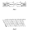
- a data transmission system includes transmitting terminal equipment 1, a modulator 2, a data transmission (e.g. telephone) line 3, a demodulator 4, and receiving terminal equipment 5.
- the transmitting terminal equipment 1 It has been normal practice for the transmitting terminal equipment 1 to send signals to the modulator 2 via a sending request signal line RS and sending data line SD. According to a rule governing interactions between the transmitting terminal equipment 1 and the modulator 2, the transmitting terminal equipment 1 supplies mark polarity data (equivalent to data of level "1") to the sending data line SD when there is no information to be sent from the transmitting terminal equipment to the receiving terminal equipment 5. (At this time the transmitting terminal equipment also supplies a "0" level to sending request signal line RS).
- transmitting terminal equipment 1 When information to be given and a data pattern to be sent are determined in the transmitting terminal equipment 1, transmitting terminal equipment 1 changes the sending request signal line RS from the "0" level (earth level, for example), to a "1" level (+12 volts or 5 volts, for example).
- the modulator 2 modulates carrier with the mark polarity data and data including the data pattern to be sent and then sends the carrier to the line 3.
- the demodulator 4 first detects the carrier of a signal received from line 3 and informs the receiving terminal equipment 5 that there is incoming data by changing the level of a carrier detection signal line CD from a "0" level to a "1" level.
- the demodulator 4 regenerates the transmitted data from the received signal and sends it to the receiving terminal equipment 5 via a receiving data line RD.
- periods wherein effective data exists are made known to the receiver by the expedient of converting data input to the modulator for such periods into specified formate. It is then sufficient to provide in the system, for discrimination of periods when effective data exists, a data converter, a decoder and a circuit for detecting data conversion.
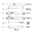
- waveform (a) illustrates a carrier as mentioned above
- waveform (b) illustrates the sending request signal mentioned above
- waveform (c) illustrates sending data to be supplied to the modulator
- waveform (d) illustrates data demodulated by the demodulator
- waveform (e) illustrates a detection signal indicating an effective data sending period
- waveform (f) illustrates received data which the receiving terminal equipment obtains from the demodulator.
- Condition 1 - when the sending request signal of waveform (b) is at a level "0";
- the modulator modulates the carrier with a continuous mark signal (All Mark) which is continuously supplied from the transmitting terminal station to the sending data signal line SD during this period and sends the modulated carrier along the line (e.g. telephone line) 3 of Figure 1.
- the demodulator on the receiving side of the system embodying this invention demodulates only the continuous mark signal and sends a detection signal to the receiving terminal equipment at a level "0".
- this detection signal takes the place of the carrier detection signal of the previous system mentioned above and, for convenience, may still be referred to as a "carrier detection signal”.
- the transmitting terminal equipment When the sending request signal is at level "1", the transmitting terminal equipment is requesting signal sending. In response the modulator encodes data (see waveform (c)), being supplied from the transmitting terminal equipment via line SD in accordance with rules A, B as explained below, after the rise time t, at which the sending request signal rises to level ".1” .
- the modulator modulates the carrier of waveform (a) with the data as illustrated in waveform (d) which has been subjected to the abovementioned conversion in accordance with A and B and sends the carrier so modulated to the line.
- the data as illustrated in (d) is demodulated from the carrier at the receiving side.
- demodulator side means are provided for detecting and decoding the data of waveform (d) consistent with rules A, B as will be explained later.
- the data bit of space polarity (provided in accordance with rule A) is detected in the demodulated data, and the detection signal (i.e. the carrier detection signal) of waveform (e) is to set level "1" consistently with the said rule A.
- the relevant data bit of space polarity is encoded (re-inverted) to mark polarity and sent to the receiving terminal equipment.
- the demodulator changes the level of carrier detection signal (e) from “0" to "1" at a delay At 2 after t 2 , for example corresponding to a period in which bit data of mark polarity has continued for a predetermined number of bits, for example 48 bits.
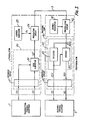
- 21 is an interface circuit
- 22 is a sending code converter
- 23 is a carrier generator used for modulation
- 24 is a modulating circuit
- 41 is a carrier generator used for demodulation
- 42 is a demodulating circuit
- 43 is a receiving unit
- 45 is a detector
- 44 is a decoder
- 46 is an interface circuit.
- the interface circuits 21 and 46 are respectively connected with plurality of interface signal lines in accordance with the above mentioned CCITT (The International Brass and Telephone Consultative Committee) Recommendation V 29.
- CCITT The International Brass and Telephone Consultative Committee
- Figure 3 shows only sending request signal line RS, sending data signal line SD, carrier detection signal line CD and receiving data signal line RD.
- Sending request signal line RS and sending data signal line SD are connected to the sending code converter 22 via the interface circuit 21.
- the sending code converter 22 carries out code conversion for signals supplied to the sending data signal line SD from the terminal equipment 1 in dependence upon the signal level supplied to the sending request signal line RS, and outputs converted sending data signals along an output line SD'.
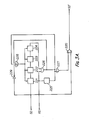
- Figure 3A shows in detail a possible configuration of the sending code converter 22.
- Fig. 3A 221, 222, 223, 224 are respective 1-bit registers, together forming a shift register by series connection.
- 225 is a differentiation circuit;
- 226 is an AND gate;
- 227, 228 are OR gates;
- 229 is an inverter; and
- 220 is an exclusive OR gate.
- An output from the AND gate 226 is at a level "0" and an output of the differentiation circuit 225 is brought to a level "0".
- mark polarity data on the sending data signal line SD is output directly onto the output line SD'.
- the differentiation circuit 225 provides an output pulse of a level "1" when the level of the sending request signal line RS changes from “0" to 11 1 ".
- mark polarity data is inverted to space polarity data by exclusive OR gate 220.
- the 1-bit registers 221, 222, 223, 224 are cleared and placed in a level "0" condition by the pulse output of differentiation circuit 225 supplied to the registers via OR gate 228.
- AND gate 226 is set in the open state.
- the sending code converter 22 executes processing in accordance with aforementioned rule A.
- the mark polarity data is supplied bit by bit to the register 221 and is sequentially shifted through the registers 222, 223, 224.
- the sending data is also concurrently input to exclusive OR gate 220 and inverter 229.
- the inverter 229 output is at a level "1" when space polarity data is fed to its input and this clears registers 221, 222, 223, 224 via the OR gate 228.
- inverter 229 output is at a "0" level when mark polarity data is fed to its input, and the registers are not cleared by such mark polarity data.
- an output of level "1" cannot be obtained from the register 224 forming the final shift register stage unless mark polarity data is supplied as sending data continuously for at least 4 bits. Namely, whilst 4 bits of mark polarity data are being shifted into the registers 221, 222, 223, 224, this sending data is output unchanged to the output line SD' via the exclusive OR gate 220. When 4 consecutive bits of mark polarity data have been received from line SD, the output signal of the register 224 attains the level "1" and is supplied to exclusive OR gate 220 via AND gate 226 and OR gate 227.
- exclusive OR gate 220 outputs 5th bit of sending data following the last space polarity data which cleared registers 221 to 224 after converting that 5th bit to space polarity if it was originally of mark polarity or after converting it to mark polarity if it was originally of space polarity.
- the modulating circuit 24 always receives a signal of specified frequency from the carrier generator 23.
- the modulating circuit 24 is, for example, so structured that it can modulate the carrier in such a way that 16 kinds of data can be indicated in accordance with amplitude and phase of the carrier. Therefore, the modulating circuit 24 firstly separates the data output from the sending code converter 22 into 4-bit sections. Then, for each four-bit section the modulating circuit 24 modulates the carrier into a signal having phase and amplitude corresponding to the data pattern carried by the relevant four bits and sends that signal to the line 3.
- the demodulating circuit 42 in the demodulator 4 receives a signal transmitted along the line 3. Moreover, the demodulating circuit 42 is supplied with a carrier, from carrier generator 41, which is similar to the carrier generated by the carrier generator 23 on the modulator side.
- the carrier generator 41 is adjusted by a carrier automatic phase controller, which is not illustrated, by well known means. On account of this adjustment, the carrier on the line can be equalized.
- the demodulating circuit 42 discriminates the phase and amplitude of a received signal with reference to the standard carrier signal sent from the abovementioned carrier generator 41, and outputs along output line RDO a data signal the same as the data signal which passed along the sending data output line SD'.
- the demodulator 42 outputs a receiving timing signal, namely timing pulses for discriminating data bits in the data output along line RDO.
- Signals on the two lines RDO and RT are supplied to the receiving unit 43 and input to detector 45, decoder 44, respectively.
- the detector 45 in the receiving unit 43 sets its carrier detection signal line CD1 to a level "1".
- the decoder 44 decodes the demodulated data in dependence upon the level of the carrier detection signal line CD1.
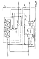
- Figure 3B shows in detail a possible configuration for the receiving unit 43.
- Blocks in Figure 3B corresponding to blocks in Fig. 3 are given the same reference numerals as in Fig. 3 and lines in Figure 3B corresponding to lines in Fig. 3 are given the same references as in Fig. 3.
- Fig. 3B 441, 442, 443, 444 are respective 1-bit registers, forming a shift register by series connection.
- 452 is a counter; 456 is a JK type flip-flop; 445, 454, 455, 457 are AND gates; 446, 447 are OR gates; 440 is an exclusive OR gate; and 451, 453 are inverters.
- AND gate 454 of detector 45 is opened by demodulated mark polarity data on line RDO.
- AND gates 455, 457 are closed via the inverters 453, 451.
- a timing pulse on receiving timing signal line RT is supplied to a counter terminal C of the counter 452 via the AND gate 454.
- the counter 454 counts the number of consecutive mark polarity data bits which occur by counting the number of timing pulses which are supplied to terminal C.
- the counter 452 When the counter 452 reaches a specified count value, for example, 48, corresponding to 48 consecutive mark polarity data bits, it provides an output signal of level "1" along a line CR. This output signal is input to the terminal K of the JK flip-flop 456 for resetting that flip-flop. Thus, the Q output of flip-flop 456 is brought to level "1", whilst the Q output is brought to level "0".
- a specified count value for example, 48, corresponding to 48 consecutive mark polarity data bits
- the level of carrier detection signal line CD1 is set to "0" when mark polarity data has continued for 48 consecutive bits.
- AND gate 445 of decoder 44 is closed. Thereby, AND gate 445 has an output of the level "0". As explained above, AND gate 457 is also closed, keeping its output at level "0".
- one input terminal of exclusive OR gate 440 is set to level "0", and data on the demodulation data line RDO is transmitted unaltered to the line RD1.
- the AND gates 455, 457 are opened by the space polarity data bit which is inverted to level "1" by the inverters 453, 451.
- the flip-flop 456 makes effective an input of terminal K with the timing pulse next to that where the counter 452 is reset as will be explained later and the counter 452 keeps the line CR at the level "0".
- the Q output of flip-flop 456 is at level "1" when this space polarity data bit appears.
- the result is that the space polarity data bit is inverted by the inverter 451, and the AND gate 457 is opened, so that during the period when a signal of level_"1" is supplied to the AND gate 457 from the Q output of 456 the output of the AND gate 457 is a signal of level "1".
- OR gate 446 the signal of level "1" from AND gate 457 causes the exclusive OR gate 440 to invert space polarity data bit to mark polarity and output that mark polarity data bit along line RD1.
- the AND gate 454 is closed and AND gate 455 is opened in response to a space polarity data bit on line RDO, and then a timing pulse from line RT is input, via 455, to terminal R of counter 452 for resetting the counter. After reset the counter keeps line CR at level "0". This results in the Q output of flip flop 456 going to "1".
- the receiving unit 43 carries out a decoding operation corresponding to coding as prescribed by abovementioned rule A.
- the Q output of flip-flop 456 is set to level "1" by space polarity data bit. Thereby, AND gate 445 is opened. Moreover, the registers 441, 442, 443, 444 are reset by an output signal of level "1" from inverter 451, through OR gate 447.
- the four mark polarity data bits are sequentially shifted, in accordance with receiving timing (by means of timing pulses supplied to the registers from line RT), through registers 441, 442, 443 and 444.
- receiving timing by means of timing pulses supplied to the registers from line RT
- registers 441, 442, 443 and 444 When a mark polarity data bit has been shifted through to register 444, an output signal of level "1" from the register 444 causes the polarity of a 5th data bit (i.e. the bit immediately following the four bits shifted into the registers) to be inverted by action of exclusive OR gate 440 controlled via AND gate 445 and OR gate 446.
- the receiving unit 43 executes a decoding operation corresponding to coding as prescribed by abovementioned rule B.
- the output signal of level "1" from 445 clears registers 441 to 444 through OR gate 447. If a further four consecutive mark polarity data bits are received after the 5th bit the next bit following the further four bits is inverted, and so on.
- the transmitting terminal equipment In a period when only mark polarity data exists the transmitting terminal equipment has set the sending request signal line RS to the level "0" as explained previously; namely it does not require data transmission.
- the number of consecutively received bits of mark polarity data are counted by the counter 452 as mentioned previously.
- counter 452 is never reset, therefore in a period when only mark polarity data exists, the counter 452 is never reset by space polarity data.
- the counter 452 counts, for example, 48 consecutive bits of mark polarity and then supplies an output signal of level "1" to the output line CR.
- the flip-flop 456 is reset and its Q output is then kept at level "0".
- the signal level of the carrier detection signal supplied line CD1 is changed from “1" " to "0".
- the receiving unit 43 outputs signals in dependence upon the signals appearing on sending request signal line RS and sending data signal line SD from the transmitting terminal equipment 1 to carrier detection signal line CD1 and data signal line RD1.
- Interface circuit 46 sends the signals on lines CD1 and RD1 to the receiving terminal equipment 5 via lines CD and RD.
- Figure 4 shows a block diagram of the system for realizing data transmission between a plurality of transmitting terminal equipments and a corresponding plurality of receiving terminal equipments on a time division multiplex basis.
- 11 to 14 are transmitting terminals; 2A1 to 2A4 are input ports; 25 and 47 are multiplexers; 4A1 to 4A4 are output ports; 51 to 54 are receiving terminals.
- Each of the input ports 2A1 to 2A4 has a structure the same as that of part 2a indicated by a broken line rectangle in Figure 3.
- each input port includes an interface circuit and a code converter operable as described above. Detailed explanation of the input ports will therefore be omitted.
- each of the output ports 4A1 to 4A4 has a structure same as that of part 4a indicated by a broken line rectangle in Fig. 3.
- each output port includes a detector and a decoder operable as described above. Detailed explanation of the output ports will therefore be omitted.
- the transmission rate of each port is, for example, 2400 BPS and transmission on the line 3 may be effected at a rate of, for example, 9600 BPS.
- Each of the transmitting terminals 11 to 14 has sending data and sending request signal lines, as provided for the transmission terminal equipment 1 of Figure 3, connected to the corresponding input port 2A1 to 2A4.
- the sending data signal lines are shown as 1 SD to 4SD in Fig. 4 and the sending request signal lines are shown as 1 RS to 4RS in Fig. 4.
- the receiving terminals 51 to 54 have receiving data lines (1RD to 4RD) and carrier detection signal lines (1CD to 4CD), as provided for the receiving terminal equipment 5 of Figure 3, connected to the corresponding output ports 4A 1 to 4A4.
- the multiplexer 25 in the modulator 2 of Figure 4 multiplexes data #1 SD, #2SD, #3SD, #4SD which is supplied to each port 2A1 to 2A4 from terminals 11 to 14 via sending data lines 1SD, 2SD, 3SD, 4SD.
- the modulator 24 modulates the multiplexed data at the rate, for example, of 9600 BPS and sends it to the line 3.
- the demodulating circuit 42 in the demodulator 4 on the receiving side regenerates received data and develops receiving timing pulses from the signal received from line 3 as explained previously.
- the data is sent along a line RD to multiplexer 47 and receiving timing pulses are sent along a line RT to multiplexer 47.
- the multiplexer (demultiplexer) 47 distributes data and receiving timing pulses to the ports 4A1 to 4A4 by counting the receiving timing pulses.
- Each port 4A1 to 4A4 receives data along a line corresponding to line RDO of Figure 3 and receives timing pulses along a line . corresponding to line RT of Figure 3.
- the regenerated received data sent to the corresponding port 4A1 to 4A4 has been subjected to inversion of bits as compared with the original sending data from the transmission terminal concerned.
- the inversion is effected in the port 2A1 to 2A4 concerned, so long as a sending request signal is supplied to that port 2A1 to 2A4 from the corresponding transmission terminal. If such a sending request signal is not being supplied, the distributed received data is all of mark polarity.
- timing pulses for respective ports 4A1 to 4A4 are only those timing pulses corresponding to the distributed receiving data for those respective ports.
- the level of the carrier detection signal line going from the port to the receiving terminal corresponding to the port changes in accordance with changes in level of the sending request signal line of the relevant remote transmitting terminal.
- the receiving side upon demodulation the level of the signal (carrier detection signal) indicating whether a data sending period is or is not an effective data sending period is changed to "0", from "1", when receiving data of continuous mark polarity continues for a predetermined number, for example, forty eight bits or more.
- the receiving side recognizes a change of value of a sending request signal on the transmitting side.
- the sending code converter 22 in Fig. 3 is provided to give the necessary guarantee by carrying out bit inversion of sending data bits, i.e. every fifth bit of mark polarity data, for example, is inverted before transmission so long as the level of the sending request signal is "1".
- sending data is, so long as it is effective data, in a format composed of data words each containing seven bits of data and one parity bit.
- such effective sending data comprises data bits and, for example, parity bits generated on an odd parity basis (generation on an even parity basis is also allowable), organised in units (words) of 8 bits.
- theoretical sending data as shown at the top of Figure 5 involves a contradiction of parity bit values.
- Chart levels I to VII in Figure 5 represent respectively the eight different phases in which the sending data at the top of Figure 5 could be taken and divided into 8-bit words. For any phase a parity bit contradiction will arise within 48 bits of data.
- the sending data is effective data, it should never have a pattern as shown at the top of Fig. 5 and it is therefore very rare for the carrier detection signal to change erroneously to level "0" on the receiving side.
- the transmission rate of sending data is 2400 BPS and a timer for counting the mark polarity data in the demodulator on the receiving side has to detect continuous mark bits for more than 48 consecutive bits before the carrier detection signal changes from level "1" to level "0"
- the probability of erroneous detection of forty eight consecutive bits of all mark data is such that this event should occur once in every 2 48 x48/2400 (sec), considering the sending data as random data and taking the number of times that sequences of forty-eight bits can be received during a second as 2400/48.
- Such a probability means that such an error occurs once in about every 6x 10 5 years and therefore the risk of carrier erroneously being dropped is almost perfectly eliminated.
- the detection of 48 consecutive mark polarity bits is used on the receiving side to determine when an effective data sending period has ended.
- effective data consists of eight bit words, each word of seven data bits and one parity bit, and that bit inversion is carried out on the transmitting side after every sequence of four mark polarity bits, parity considerations ensure that 48 consecutive mark polarity bits cannot (without error) be received on the receiving side as effective data.
- a transmitter continuously transmits a carrier to a receiver and modulates the carrier with sending data and wherein a receiver demodulates the data.
- the transmitter converts the specified bits of the sending data and then transmits the converted data and the receiver discriminates effective sending data in dependence upon detection of such conversion in received data.
Landscapes
- Engineering & Computer Science (AREA)
- Signal Processing (AREA)
- Computer Networks & Wireless Communication (AREA)
- Physics & Mathematics (AREA)
- Spectroscopy & Molecular Physics (AREA)
- Communication Control (AREA)
- Time-Division Multiplex Systems (AREA)
Claims (5)
Applications Claiming Priority (2)
| Application Number | Priority Date | Filing Date | Title |
|---|---|---|---|
| JP24257/79 | 1979-03-02 | ||
| JP54024257A JPS6030460B2 (ja) | 1979-03-02 | 1979-03-02 | キヤリヤ検出信号制御方式 |
Publications (2)
| Publication Number | Publication Date |
|---|---|
| EP0015730A1 EP0015730A1 (fr) | 1980-09-17 |
| EP0015730B1 true EP0015730B1 (fr) | 1984-12-27 |
Family
ID=12133182
Family Applications (1)
| Application Number | Title | Priority Date | Filing Date |
|---|---|---|---|
| EP80300612A Expired EP0015730B1 (fr) | 1979-03-02 | 1980-02-29 | Système de transmission de données et procédé pour faire passer des données à travers un système de transmission de données |
Country Status (5)
| Country | Link |
|---|---|
| US (1) | US4317207A (fr) |
| EP (1) | EP0015730B1 (fr) |
| JP (1) | JPS6030460B2 (fr) |
| CA (1) | CA1134447A (fr) |
| DE (1) | DE3069852D1 (fr) |
Families Citing this family (17)
| Publication number | Priority date | Publication date | Assignee | Title |
|---|---|---|---|---|
| US4498186A (en) * | 1980-10-10 | 1985-02-05 | At&T Bell Laboratories | Data set diagnostic system |
| US4398297A (en) * | 1980-10-10 | 1983-08-09 | Bell Telephone Laboratories, Incorporated | Data set diagnostic system |
| US4622685A (en) * | 1982-03-29 | 1986-11-11 | Racal Data Communications Inc. | RTS/DCD simulator |
| DE3311346A1 (de) * | 1982-03-29 | 1983-09-29 | Racal-Data Communication, Inc., 33166 Miami, Fla. | Simulator fuer sendebereitschafts- /datenempfangsbereitschaftssignale |
| JPS59112748A (ja) * | 1982-12-06 | 1984-06-29 | Fujitsu Ltd | デ−タ送受信システム |
| JPS59182648A (ja) * | 1983-03-31 | 1984-10-17 | Mitsubishi Electric Corp | 双方向信号連絡装置 |
| JPS61118032A (ja) * | 1984-11-14 | 1986-06-05 | Iwatsu Electric Co Ltd | デ−タ伝送方式 |
| US4703486A (en) * | 1984-12-18 | 1987-10-27 | Advanced Micro Devices, Inc. | Communication data encoder/decoder component system architecture |
| IT1184933B (it) * | 1985-03-28 | 1987-10-28 | Olivetti & Co Spa | Circuito di integrazione per la trasmissione e la ricezione di dati |
| US4700358A (en) * | 1985-11-18 | 1987-10-13 | Hayes Microcomputer Products, Inc. | Synchronous/asynchronous modem |
| US4738227A (en) * | 1986-02-21 | 1988-04-19 | Adiabatics, Inc. | Thermal ignition combustion system |
| EP0306585B1 (fr) * | 1987-09-10 | 1992-07-22 | International Business Machines Corporation | Système de transmission de données avec dispositif d'alarme numérique |
| EP0385042A1 (fr) * | 1989-02-28 | 1990-09-05 | International Business Machines Corporation | Méthode pour ajuster la fin de transmission dans un modem |
| US5025454A (en) * | 1989-07-17 | 1991-06-18 | The Johns Hopkins University | Pulse to zero digital (PZ) modulation |
| US5673130A (en) * | 1996-01-02 | 1997-09-30 | Motorola, Inc. | Circuit and method of encoding and decoding digital data transmitted along optical fibers |
| WO2009155006A2 (fr) * | 2008-05-27 | 2009-12-23 | Viasat, Inc . | Redondance pour modem insensible aux défaillances |
| USD903268S1 (en) | 2019-02-06 | 2020-12-01 | S. C. Johnson & Son, Inc. | Insole |
Family Cites Families (10)
| Publication number | Priority date | Publication date | Assignee | Title |
|---|---|---|---|---|
| US1901642A (en) * | 1929-12-23 | 1933-03-14 | Rca Corp | Signaling |
| DE958390C (de) * | 1954-09-01 | 1957-02-21 | Philips Nv | Schaltungsanordnung zum UEbertragen eines Dienstzeichens bei rhythmischen Telegraphensystemen |
| US3457550A (en) * | 1967-07-11 | 1969-07-22 | Bell Telephone Labor Inc | Automatic handshaking method and apparatus for data transmission systems |
| GB1156279A (en) * | 1967-12-20 | 1969-06-25 | Standard Telephones Cables Ltd | Data Transmission Terminal |
| US3633168A (en) * | 1971-03-09 | 1972-01-04 | Ibm | Line control adapter for a synchronous digital-formatted message-communications system |
| IT1021004B (it) * | 1973-11-09 | 1978-01-30 | Honeywell Inf Systems | Apparecchiatura elettronica di co mando di periferica per il collega mento locale e remoto della stessa ad un sistema di elaborazione dati |
| US3898388A (en) * | 1974-06-21 | 1975-08-05 | United Aircraft Corp | Phase inversion synchronization |
| US4161719A (en) * | 1977-10-04 | 1979-07-17 | Ncr Corporation | System for controlling synchronization in a digital communication system |
| US4208650A (en) * | 1978-01-30 | 1980-06-17 | Forney Engineering Company | Data transmission system |
| DE2809775C2 (de) * | 1978-03-07 | 1985-10-10 | Siemens AG, 1000 Berlin und 8000 München | Elektrische Fernbedienungsanlage |
-
1979
- 1979-03-02 JP JP54024257A patent/JPS6030460B2/ja not_active Expired
-
1980
- 1980-02-29 DE DE8080300612T patent/DE3069852D1/de not_active Expired
- 1980-02-29 EP EP80300612A patent/EP0015730B1/fr not_active Expired
- 1980-03-03 US US06/126,527 patent/US4317207A/en not_active Expired - Lifetime
- 1980-03-03 CA CA000346849A patent/CA1134447A/fr not_active Expired
Also Published As
| Publication number | Publication date |
|---|---|
| JPS55117355A (en) | 1980-09-09 |
| DE3069852D1 (en) | 1985-02-07 |
| US4317207A (en) | 1982-02-23 |
| EP0015730A1 (fr) | 1980-09-17 |
| CA1134447A (fr) | 1982-10-26 |
| JPS6030460B2 (ja) | 1985-07-16 |
Similar Documents
| Publication | Publication Date | Title |
|---|---|---|
| EP0015730A1 (fr) | Système de transmission de données et procédé pour faire passer des données à travers un système de transmission de données | |
| CA1172331A (fr) | Systeme de transmission de donnees a auto- synchronisation | |
| AU583033B2 (en) | Data and voice communications system | |
| US3310631A (en) | Communication system for the selective transmission of speech and data | |
| JPH0691520B2 (ja) | フレ−ム同期はずれ検出方式 | |
| US4011511A (en) | Frequency-shift digital data link and digital frequency detection system | |
| US3936609A (en) | Submultiplex transmission of alarm status signals for a time division multiplex system | |
| EP0306585B1 (fr) | Système de transmission de données avec dispositif d'alarme numérique | |
| US4864617A (en) | System and method for reducing deadlock conditions caused by repeated transmission of data sequences equivalent to those used for inter-device signalling | |
| US3969582A (en) | System for automatic synchronization of blocks transmitting a series of bits | |
| GB2131656A (en) | Dc cancellation in ternary-coded data systems | |
| JP2973722B2 (ja) | 遠隔監視方式 | |
| JP2767107B2 (ja) | フレームフォーマット変換方法 | |
| JPH03219745A (ja) | 極性判定回路 | |
| US4952070A (en) | Digital data coding technique | |
| JPS59172871A (ja) | 受信用多チヤネル分離装置に適用されるチヤネル同期回路 | |
| GB1597835A (en) | Error detection arrangements for line transmission systems | |
| US3963867A (en) | Method for indicating a free-line state in a binary data communication system | |
| GB2243056A (en) | Repeater supervision | |
| WO1995009496A1 (fr) | Procede de transmission numerique semi-duplex | |
| SU563734A1 (ru) | Устройство дл контрол многоканальной системы св зи с временным разделением каналов | |
| JPS63151131A (ja) | 時分割多重伝送方式 | |
| JPS6282835A (ja) | 時分割多方向多重通信方式 | |
| JPS60189353A (ja) | ステ−タス情報伝送方法およびその装置 | |
| JPS6272240A (ja) | ステ−タス信号伝送装置 |
Legal Events
| Date | Code | Title | Description |
|---|---|---|---|
| PUAI | Public reference made under article 153(3) epc to a published international application that has entered the european phase |
Free format text: ORIGINAL CODE: 0009012 |
|
| AK | Designated contracting states |
Designated state(s): DE FR GB NL SE |
|
| 17P | Request for examination filed |
Effective date: 19810227 |
|
| GRAA | (expected) grant |
Free format text: ORIGINAL CODE: 0009210 |
|
| AK | Designated contracting states |
Designated state(s): DE FR GB NL SE |
|
| REF | Corresponds to: |
Ref document number: 3069852 Country of ref document: DE Date of ref document: 19850207 |
|
| ET | Fr: translation filed | ||
| PLBE | No opposition filed within time limit |
Free format text: ORIGINAL CODE: 0009261 |
|
| STAA | Information on the status of an ep patent application or granted ep patent |
Free format text: STATUS: NO OPPOSITION FILED WITHIN TIME LIMIT |
|
| REG | Reference to a national code |
Ref country code: GB Ref legal event code: 732 |
|
| 26N | No opposition filed | ||
| REG | Reference to a national code |
Ref country code: FR Ref legal event code: TP |
|
| NLS | Nl: assignments of ep-patents |
Owner name: NIPPON TELEGRAPH AND TELEPHONE CORPORATION TE TOKI |
|
| EAL | Se: european patent in force in sweden |
Ref document number: 80300612.1 |
|
| PGFP | Annual fee paid to national office [announced via postgrant information from national office to epo] |
Ref country code: SE Payment date: 19990204 Year of fee payment: 20 |
|
| PGFP | Annual fee paid to national office [announced via postgrant information from national office to epo] |
Ref country code: FR Payment date: 19990209 Year of fee payment: 20 |
|
| PGFP | Annual fee paid to national office [announced via postgrant information from national office to epo] |
Ref country code: NL Payment date: 19990224 Year of fee payment: 20 |
|
| PGFP | Annual fee paid to national office [announced via postgrant information from national office to epo] |
Ref country code: GB Payment date: 19990304 Year of fee payment: 20 |
|
| PGFP | Annual fee paid to national office [announced via postgrant information from national office to epo] |
Ref country code: DE Payment date: 19990305 Year of fee payment: 20 |
|
| PG25 | Lapsed in a contracting state [announced via postgrant information from national office to epo] |
Ref country code: SE Free format text: THE PATENT HAS BEEN ANNULLED BY A DECISION OF A NATIONAL AUTHORITY Effective date: 20000227 |
|
| PG25 | Lapsed in a contracting state [announced via postgrant information from national office to epo] |
Ref country code: GB Free format text: LAPSE BECAUSE OF EXPIRATION OF PROTECTION Effective date: 20000228 |
|
| PG25 | Lapsed in a contracting state [announced via postgrant information from national office to epo] |
Ref country code: NL Free format text: LAPSE BECAUSE OF EXPIRATION OF PROTECTION Effective date: 20000229 |
|
| REG | Reference to a national code |
Ref country code: GB Ref legal event code: PE20 Effective date: 20000228 |
|
| NLV7 | Nl: ceased due to reaching the maximum lifetime of a patent |
Effective date: 20000229 |
|
| EUG | Se: european patent has lapsed |
Ref document number: 80300612.1 |