EP0017032A2 - Procédé de fabrication d'un dispositif à l'état solide par décapage différentiel par plasma des couches résistantes - Google Patents
Procédé de fabrication d'un dispositif à l'état solide par décapage différentiel par plasma des couches résistantes Download PDFInfo
- Publication number
- EP0017032A2 EP0017032A2 EP80101269A EP80101269A EP0017032A2 EP 0017032 A2 EP0017032 A2 EP 0017032A2 EP 80101269 A EP80101269 A EP 80101269A EP 80101269 A EP80101269 A EP 80101269A EP 0017032 A2 EP0017032 A2 EP 0017032A2
- Authority
- EP
- European Patent Office
- Prior art keywords
- film
- monomer
- polymer
- monomers
- nanometers
- Prior art date
- Legal status (The legal status is an assumption and is not a legal conclusion. Google has not performed a legal analysis and makes no representation as to the accuracy of the status listed.)
- Granted
Links
Images
Classifications
-
- G—PHYSICS
- G03—PHOTOGRAPHY; CINEMATOGRAPHY; ANALOGOUS TECHNIQUES USING WAVES OTHER THAN OPTICAL WAVES; ELECTROGRAPHY; HOLOGRAPHY
- G03F—PHOTOMECHANICAL PRODUCTION OF TEXTURED OR PATTERNED SURFACES, e.g. FOR PRINTING, FOR PROCESSING OF SEMICONDUCTOR DEVICES; MATERIALS THEREFOR; ORIGINALS THEREFOR; APPARATUS SPECIALLY ADAPTED THEREFOR
- G03F7/00—Photomechanical, e.g. photolithographic, production of textured or patterned surfaces, e.g. printing surfaces; Materials therefor, e.g. comprising photoresists; Apparatus specially adapted therefor
- G03F7/26—Processing photosensitive materials; Apparatus therefor
- G03F7/36—Imagewise removal not covered by groups G03F7/30 - G03F7/34, e.g. using gas streams, using plasma
-
- G—PHYSICS
- G03—PHOTOGRAPHY; CINEMATOGRAPHY; ANALOGOUS TECHNIQUES USING WAVES OTHER THAN OPTICAL WAVES; ELECTROGRAPHY; HOLOGRAPHY
- G03F—PHOTOMECHANICAL PRODUCTION OF TEXTURED OR PATTERNED SURFACES, e.g. FOR PRINTING, FOR PROCESSING OF SEMICONDUCTOR DEVICES; MATERIALS THEREFOR; ORIGINALS THEREFOR; APPARATUS SPECIALLY ADAPTED THEREFOR
- G03F7/00—Photomechanical, e.g. photolithographic, production of textured or patterned surfaces, e.g. printing surfaces; Materials therefor, e.g. comprising photoresists; Apparatus specially adapted therefor
- G03F7/004—Photosensitive materials
- G03F7/027—Non-macromolecular photopolymerisable compounds having carbon-to-carbon double bonds, e.g. ethylenic compounds
- G03F7/032—Non-macromolecular photopolymerisable compounds having carbon-to-carbon double bonds, e.g. ethylenic compounds with binders
- G03F7/033—Non-macromolecular photopolymerisable compounds having carbon-to-carbon double bonds, e.g. ethylenic compounds with binders the binders being polymers obtained by reactions only involving carbon-to-carbon unsaturated bonds, e.g. vinyl polymers
-
- H—ELECTRICITY
- H10—SEMICONDUCTOR DEVICES; ELECTRIC SOLID-STATE DEVICES NOT OTHERWISE PROVIDED FOR
- H10P—GENERIC PROCESSES OR APPARATUS FOR THE MANUFACTURE OR TREATMENT OF DEVICES COVERED BY CLASS H10
- H10P50/00—Etching of wafers, substrates or parts of devices
- H10P50/20—Dry etching; Plasma etching; Reactive-ion etching
- H10P50/28—Dry etching; Plasma etching; Reactive-ion etching of insulating materials
- H10P50/286—Dry etching; Plasma etching; Reactive-ion etching of insulating materials of organic materials
- H10P50/287—Dry etching; Plasma etching; Reactive-ion etching of insulating materials of organic materials by chemical means
-
- Y—GENERAL TAGGING OF NEW TECHNOLOGICAL DEVELOPMENTS; GENERAL TAGGING OF CROSS-SECTIONAL TECHNOLOGIES SPANNING OVER SEVERAL SECTIONS OF THE IPC; TECHNICAL SUBJECTS COVERED BY FORMER USPC CROSS-REFERENCE ART COLLECTIONS [XRACs] AND DIGESTS
- Y10—TECHNICAL SUBJECTS COVERED BY FORMER USPC
- Y10S—TECHNICAL SUBJECTS COVERED BY FORMER USPC CROSS-REFERENCE ART COLLECTIONS [XRACs] AND DIGESTS
- Y10S430/00—Radiation imagery chemistry: process, composition, or product thereof
- Y10S430/167—X-ray
- Y10S430/168—X-ray exposure process
Definitions
- This invention relates to producing solid state devices by a plasma processing technique for feature delineation. More particularly, the invention relates to plasma etching of an irradiated resist film having at least one type of monomer locked into a host polymer to produce the desired negative resist pattern.
- Plasmas have been used for several years to etch substrate materials, or for stripping away photoresists after a conventional liquid etch. They have also been used for selective etching when the pattern to be etched has first been defined by conventional means; see U. S. Patents 3,816,196; 3,816,198. However, the use of plasmas to etch the pattern in the first instance is known by the present inventor in only one previous publication, German patent (Offen) 27 26 813.
- This invention relates to a new technique for producing negative resist patterns in the process of producing solid state devices. It makes use of a plasma having a differential rate of etch in the irradiated and unirradiated regions of the resist. Since it is a dry etching process, the resolution is not limited by swelling of the resist due to absorption of developing solution.
- the pattern may be formed directly on a wafer or an intermediate layer on a wafer for making semiconductor devices such as large scale integrated circuits, or other solid state devices, such as bubble memories. Alternately, the pattern may be used to form a master mask that is separate from the device being produced.
- a polymer host material is mixed with one or more types of monomer, said monomer or monomers forming a "monomer material" that is sensitive to electromagnetic radiation in said polymer.
- the resulting material usually dissolved in a liquid solvent, is coated onto a substrate and the solvent is allowed to evaporate.
- the resulting film is selectively irradiated by the proper wavelength radiation, such as visible or ultraviolet light, or X-rays, either directly or through a mask that delineates the desired pattern on the resist film.
- the resist film is then etched by means of a plasma, which preferentially removes material from the host-polymer-only portion of the film. Although the monomer-retained portion of the film is also attacked by the plasma, it is removed at a slower rate than the polymer-only portion. When the polymer-only portion has been removed down to the substrate, a resist pattern is obtained which corresponds to the radiation pattern, hence yielding a negative tone resist pattern.
- the following description covers new negative resist material and a dry etch development process.
- the materials are mixtures of a host polymer of low volatility and one or more moderately volatile monomers which are locked into the host polymer by electromagnetic radiation.
- the unlocked monomer material is then substantially removed from the film by heating, or a vacuum, or both. Pattern development is accomplished by exposure to a plasma.
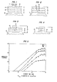
- FIG. 1 a resist layer 12, comprising a mixture of monomer 13 and host polymer 14 molecules, is shown formed on substrate 15, the layer being of suitable thickness 16.
- the resist layer is selectively irradiated by a beam of electromagnetic radiation 11, either directly or through a mask (not shown).
- FIG. 2 shows how the monomer material may form links 21 and 22 in the irradiated region.
- Link 21 is between two monomers, which may be of the same or different monomer types, while link 22 is between a monomer and a host polymer.
- the linking of the two monomers, whether of the same or different types, is hereafter referred to as dimerization.
- the linking of more than two monomers in a chain is referred to hereafter as polymerization, whether the monomers in the chain are of the same or different types.
- the linking of a monomer to a host polymer is referred to hereafter as attachment, and the attachment of a monomer followed by the linking of one or more monomers to the attached monomer is referred to as grafting, again whether the monomers are of the same or different types.
- the monomers outside the irradiated region remain unlinked.
- the thickness 16 of the irradiated region 31 may become less than that of the resist film prior to the fixing step
- the thickness 37 of the unirradiated region 32 from which the monomers have been removed may be slightly thinner than the thickness of the irradiated region, typically on the order of 1000 Angstroms (100 nanometers) thinner and typically 700 Angstroms (70 nanometers) thinner with the examples given below. This is due to the greater loss of monomer material from the unirradiated region.
- the final resist relief pattern of a thickness 47 is shown after etching in a plasma, usually at an elevated temperature. The plasma etched the host- polymer-only region at a faster rate than the region containing the linked monomers. This leaves resist pattern 41 in the irradiated region and bare portion 42 of substrate 15 in the unirradiated region, thus creating a negative tone resist pattern.
- the "differential etch ratio" as used herein means the ratio of the thicknesses of material removed in a given amount of time by plasma etching in the unirradiated versus the irradiated regions of the resist. For example starting with a 10,000 Angstrom (lu m) thick resist material on a substrate, which after radiation and fixing is 9500 Angstroms (950 nanometers) thick in the irradiated region and 8800 Angstroms (880 nanometers) thick in the unirradiated region, plasma etching proceeds until all the material is just removed from the unirradiated region down to the substrate. At this point, 1500 Angstroms (150 nanometers) of material is left in the radiated region. The differential etch ratio is then:
- the differential plasma etch phenomenon has been observed by the present inventor thus far for monomers containing aromatic functionality, herein also referred to as aromatic monomers, and various chlorinated polymers.
- aromatic monomers herein also referred to as aromatic monomers
- various chlorinated polymers have been obtained with the chlorinated polymer poly(2,3-dichloro-1-propyl acrylate), herein also referred to as DCPA.
- the radiation source used for obtaining the results herein is an X-ray source emitting at approximately 4.4. Angstroms (0.44 nanometers).
- All heating mixtures were developed after irradiation and heating for 1 hour at 90 degrees C and 0.1 torr (133.32 microbar) by treatment with an unshielded rf-generated oxygen plasma in an International Plasma Corporation 2005T-1813SCA Etcher. Samples were held horizontally on an Al or quartz table at the bottom of the reactor. Etching was conducted using a power of 100 watts at a pressure of 0.60 torr (799.92 microbar) and a temperature range from 25-60 degrees C as measured by a temperature probe mounted in the etch chamber.
- polymerizable aromatic monomers are suitable as the monomer material with a host nonaromatic polymer.
- aromatic monomers can be locked into polymeric hosts by radiation techniques; see E. A. Chandross, C. A. Pryde, W. J. Tomlinson and H. P. Weber, "Photolocking - a New Technique for Fabricating Optical Waveguide Circuits", Appl. Phys. Lett., Vol. 24, No. 2, pp. 72-74 (1974). This work formed the basis for U. S. Patent No. 3,809,732.
- An additional advantage which aids in the achievement of high aspect ratios, is that if the fixing temperature is not too high, polymerization of the above- named aromatic monomers is not thermally initiated by the heating required to remove unreacted monomer from the unirradiated region.
- the aromatic monomers given above have moderate volatility. It is necessary that the volatility not be too high, or else the monomer material will evaporate from the host polymer before, and while, being locked in place by radiation. On the other hand, volatility should not be too low, or the heating time necessary to drive the unlocked, unirradiated monomer material out of the host polymer will be so long, or the heating temperature so high, as to thermally lock the monomer material in place. Such thermal locking reduces the differential etch ratio.
- polymeric host is also important, for it should have a high-plasma removal rate and be capable of initiating polymerization upon absorption of X-radiation. Unlike the photolocking experiments of Chandross and coworkers above, in which all the irradiating light was absorbed by the monomer, the PD La X-radiation here is absorbed primarily by the host polymer. Thus far, poly(2,3-dichloro-l-propyl acrylate) appears to be the preferred host for it has a very high removal rate in an 0 2 plasma, a high absorption to Pd La X-rays, and a favorable initiation rate, especially for cationically initiated polymerizations. In addition many monomers are highly soluble in DCPA and it can be prepared in quantity.
- the high etch rate is apparantly due to the presence of chlorine atoms in the side chains of DCPA. These chlorine atoms act as a catalyst that aids in breaking the backbone of the polymer chain. It is this combination of an anomalously high etch rate in an oxygen plasma and a high rate of initiating polymerization of irradiated monomers that makes the chlorinated polymers, and inparticular DCPA, the best host polymer materials found thus far.
- Other chlorinated polymers have been tested with NVC as the sole monomer, with results indicated in Table III. To show the relative rates of removal of each polymer in an oxygen plasma, poly(styrene) has been chosen as a reference, with an arbitrary assignment of its removal rate as 1.0. To obtain a high differential etch ratio, the polymer should not be an aromatic polymer, if an aromatic monomer or monomers are used.
- brominated polymers may be very useful as the host material, as they absorb relatively well the X-ray wavelengths around 4.6 Angstroms (0.46 nanometers) and 5.4 Angstroms (0.54 nanometers), among others. These wavelengths are produced by electron bombardment of rhodium and molybdenum targets, respectively. These are preferred targets in many cases due to their ability to withstand greater power densities and thus produce higher X-ray output powers than most other targets. Also, brominated polymers are removed by an oxygen plasma, although not as rapidly as chlorinated polymers tested thus far.
- the characteristics of the oxygen plasma have an important effect on the etching process. Firstly, the etching process proceeds more rapidly the higher the temperature of the etching system. However, too high a temperature leads to disadvantageous formation of particulate deposits of organic material on the film. Further, the rate of removal may become too high for precise control of the stop time if the temperature is too high. Temperatures in the range of 20 degrees C (ambient room temperature) to 60 degrees C have been found suitable for the DCPA-NVC combination, with even higher temperatures possible. Secondly, the oxygen plasma used for the examples given herein was obtained in a "barrel" type plasma reactor of the type previously noted, but improved uniformity has been found in many cases when a reactive ion etcher was employed.
- the plasma referred to herein may be produced by either type apparatus, with still others being possible.
- the reactive ion etcher imparts an electrical bias to the substrate and accelerates the ions across a "dark space".
- the removal of resist material is still primarily due to chemical reaction, in turn dependent upon reactant species in the oxygen plasma.
- plasma etching is to be distinguished from procedures, such as ion milling, where momentum exchange is the primary removal mechanism. It is, of course, inherent that some momentum exchange occurs due to the plasma field itself. Accordingly, whereas resist removal is not primarily due to momentum exchange, momentum exchange does occur and, in fact, may be responsible in part for initiating or enhancing chemical activity.
- the step of fixing the pattern after irradiation varies with the specific monomer or monomers and polymer material used. This depends on such factors as volatility of the monomer material and the degree to which the monomer-polymer film can withstand high temperatures without thermal locking of the monomer material in the host polymer.
- the fixing temperature and vacuum conditions can be varied to yield various tradeoffs in terms of differential etch.ratio versus processing speed.
- a solution containing by weight 93 parts chlorobenzene, 7 parts poly(2,3-dichloro-l-propyl acrylate) having an intrinsic viscosity [n] 2.00 dl/g in ethyl acetate at 30 degrees C and 1.64 parts N-vinylcarbazole was spincoated onto a silicon substrate at 3,500 rpm to give a 1 ⁇ m thick coating. It was selectively irradiated for 1 minute by Pd La X-radiation in an X-ray radiation system. The X-ray flux incident on the resist coating was 2.9 mj/cm 2 /min. After irradiation, the substrate was placed in a vacuum oven for 1 hour.
- the difference in removal rates for the irradiated and unirradiated regions was 320 Angstroms/min. (32 nanometers/min.).
- the differential etch ratio was 1.11. Submicrometer features were resolved.
- N-vinylcarbazole A solution containing by weight 90 parts chlorobenzene, 10 parts poly(2-chloroethyl acrylate), and 1.11 parts N-vinylcarbazole was spincoated onto a silicon substrate at 2000 rpm to give a 1.07pm thick uniform coating. Samples containing 2.5 parts N-vinylcarbazole gave nonuniform, splotchy films upon spincoating. This indicated phase separation had occurred at the higher N-vinylcarbazole concentration.
- a solution containing by weight 88 parts of chlorobenzene, 12 parts of poly(2,3-dichloro-l-propyl acrylate) and 0.63 parts N-phenylmaleimide was spincoated onto a silicon substrate at 4000 rpm to give a 1.0 ⁇ m thick coating.
- the [n] of the polymeric component was 0.80 dl/g in ethyl acetate at 30 degrees C.
- the sample was selectively irradiated as in the above examples by 2.0 minutes of X-radiation. The sample was placed in vacuum at 30 degrees C for 2 hours and then overnight at 90 degrees C also in vacuum.
- the difference in removal rates in the unirradiated and irradiated regions was 245 Angstroms/min. (24.5 nanometers/min.).
- the differential etch ratio was 1.13.
- a solution containing by weight 88 parts of chlorobenzene, 12 parts of poly(2,3-dichloro-l-propyl acrylate) and 0.63 parts diphenyldivinylsilane was spincoated onto a silicon substrate at 2000 rpm to give a 1.01 ⁇ m thick coating.
- the differential etch ratio was 1.30. Features having submicrometer dimensions were resolved.
- the difference in plasma removal rates was 380 Angstroms/min. (38 nanometers/min.).
- the differential etch ratio was 1.11. Features having submicrometer dimensions were resolved. Nearly identical results were obtained when the 2-(1 -naphthyl)ethyl acrylate was replaced with 2-(1 -napthhyl)ethyl methacrylate.
- the silane was not itself soluble in the poly(2,3-dichloro-l-propyl acrylate); the addition of N-vinylcarbazole enabled solubilization in the host polymeric material.
- the difference in removal rates was 560 Angstroms/min. (56 nanometers/min.).
- the differential etch ratio was 1.28.
- a solution containing by weight 93 parts chlorobenzene, 12 parts poly(2,3-dichloro-l-propyl acrylate), 3 parts N-phenylmaleimide, and 3 parts dimethylphenyl-4-vinylphenylsilane described in Example 8 was spincoated onto a silicon substrate at 7300 rpm to give a 1.0 m thick coating.
- the sample was selectively irradiated with X-radiation as above for 1 minute and placed under vacuum for 2 hours at 30 degrees C.
- the difference in plasma removal rates was 560 Angstroms/min. (56 nanometers/min.).
- the differential etch ratio was 1.22. Features with submicrometer dimensions were resolved.
- a solution containing by weight 88 parts chlorobenzene, 12 parts poly (2,3-dichloro-l-propyl acrylate), 2.3 parts N-vinylcarbazole, and 7.5 parts diphenyldivinylsilane was spincoated onto a silicon substrate at 6000 rpm to give a 1.0 m thick coating.
Landscapes
- Physics & Mathematics (AREA)
- General Physics & Mathematics (AREA)
- Chemical & Material Sciences (AREA)
- Chemical Kinetics & Catalysis (AREA)
- Spectroscopy & Molecular Physics (AREA)
- Drying Of Semiconductors (AREA)
- Photosensitive Polymer And Photoresist Processing (AREA)
- Exposure Of Semiconductors, Excluding Electron Or Ion Beam Exposure (AREA)
- Exposure And Positioning Against Photoresist Photosensitive Materials (AREA)
- Polymerisation Methods In General (AREA)
Applications Claiming Priority (2)
| Application Number | Priority Date | Filing Date | Title |
|---|---|---|---|
| US06/019,711 US4232110A (en) | 1979-03-12 | 1979-03-12 | Solid state devices formed by differential plasma etching of resists |
| US19711 | 1979-03-12 |
Publications (3)
| Publication Number | Publication Date |
|---|---|
| EP0017032A2 true EP0017032A2 (fr) | 1980-10-15 |
| EP0017032A3 EP0017032A3 (en) | 1981-07-15 |
| EP0017032B1 EP0017032B1 (fr) | 1984-02-15 |
Family
ID=21794629
Family Applications (1)
| Application Number | Title | Priority Date | Filing Date |
|---|---|---|---|
| EP80101269A Expired EP0017032B1 (fr) | 1979-03-12 | 1980-03-12 | Procédé de fabrication d'un dispositif à l'état solide par décapage différentiel par plasma des couches résistantes |
Country Status (7)
| Country | Link |
|---|---|
| US (1) | US4232110A (fr) |
| EP (1) | EP0017032B1 (fr) |
| JP (1) | JPS56500097A (fr) |
| CA (1) | CA1134953A (fr) |
| DE (1) | DE3066537D1 (fr) |
| ES (1) | ES8103476A1 (fr) |
| WO (1) | WO1980001978A1 (fr) |
Cited By (4)
| Publication number | Priority date | Publication date | Assignee | Title |
|---|---|---|---|---|
| EP0091651A3 (en) * | 1982-04-12 | 1984-10-17 | Nippon Telegraph And Telephone Public Corporation | Method for forming micropattern |
| WO1985002030A1 (fr) * | 1983-11-02 | 1985-05-09 | Hughes Aircraft Company | MASQUES LITHOGRAPHIQUES EN SiO2 POLYMERISES PAR GREFFAGE |
| EP0184567A1 (fr) * | 1984-10-26 | 1986-06-11 | UCB Electronics, S.A. | Procédé de formation de motifs négatifs dans une couche de photorésist |
| EP0186798A3 (en) * | 1984-12-07 | 1988-09-21 | International Business Machines Corporation | Top imaged plasma developable resists |
Families Citing this family (16)
| Publication number | Priority date | Publication date | Assignee | Title |
|---|---|---|---|---|
| US4345021A (en) * | 1979-09-25 | 1982-08-17 | Matsushita Electric Industrial Co., Ltd. | Solid-state image pickup element and process for fabricating the same |
| JPS5744143A (en) * | 1980-08-29 | 1982-03-12 | Tokyo Ohka Kogyo Co Ltd | Composition and method for forming micropattern |
| JPS57157523A (en) * | 1981-03-25 | 1982-09-29 | Hitachi Ltd | Forming method for pattern |
| US4396704A (en) * | 1981-04-22 | 1983-08-02 | Bell Telephone Laboratories, Incorporated | Solid state devices produced by organometallic plasma developed resists |
| US4500628A (en) * | 1981-04-22 | 1985-02-19 | At&T Bell Laboratories | Process of making solid state devices using silicon containing organometallic plasma developed resists |
| JPS57202534A (en) * | 1981-06-09 | 1982-12-11 | Fujitsu Ltd | Negative type resist composition |
| JPS57202537A (en) * | 1981-06-09 | 1982-12-11 | Fujitsu Ltd | Resist composition for dry development |
| US4400235A (en) * | 1982-03-25 | 1983-08-23 | Bell Telephone Laboratories, Incorporated | Etching apparatus and method |
| US4665541A (en) * | 1983-06-06 | 1987-05-12 | The University Of Rochester | X-ray lithography |
| US5215867A (en) * | 1983-09-16 | 1993-06-01 | At&T Bell Laboratories | Method with gas functionalized plasma developed layer |
| US4596761A (en) * | 1983-11-02 | 1986-06-24 | Hughes Aircraft Company | Graft polymerized SiO2 lithographic masks |
| USH102H (en) | 1984-11-09 | 1986-08-05 | At&T Bell Laboratories | Controlling resolution of exposed resist in device lithography |
| US4751170A (en) * | 1985-07-26 | 1988-06-14 | Nippon Telegraph And Telephone Corporation | Silylation method onto surface of polymer membrane and pattern formation process by the utilization of silylation method |
| US5094936A (en) * | 1988-09-16 | 1992-03-10 | Texas Instruments Incorporated | High pressure photoresist silylation process and apparatus |
| KR0140472B1 (ko) * | 1994-10-12 | 1998-06-15 | 김주용 | 감광막 패턴 형성방법 |
| US7742672B2 (en) * | 2005-08-24 | 2010-06-22 | General Electric Company | Composition, optical device article, and associated method |
Family Cites Families (9)
| Publication number | Priority date | Publication date | Assignee | Title |
|---|---|---|---|---|
| BE560986A (fr) * | 1956-09-21 | |||
| US3816198A (en) * | 1969-09-22 | 1974-06-11 | G Babcock | Selective plasma etching of organic materials employing photolithographic techniques |
| US3871885A (en) * | 1971-05-18 | 1975-03-18 | Du Pont | Crystalline photo-polymerizable composition |
| US3816196A (en) * | 1971-06-07 | 1974-06-11 | Gen Electric | Passivation of photoresist materials used in selective plasma etching |
| US3809732A (en) * | 1972-12-18 | 1974-05-07 | Bell Telephone Labor Inc | Photo-locking technique for producing integrated optical circuits |
| US3916035A (en) * | 1973-11-05 | 1975-10-28 | Texas Instruments Inc | Epoxy-polymer electron beam resists |
| US3953620A (en) * | 1974-12-06 | 1976-04-27 | Bell Telephone Laboratories, Incorporated | Producing integrated optical circuits |
| DE2726813C2 (de) | 1976-06-17 | 1984-02-23 | Motorola, Inc., 60196 Schaumburg, Ill. | Verfahren zur Herstellung eines mit einem Muster versehenen Substrats |
| FR2389922B1 (fr) * | 1977-05-03 | 1981-08-28 | Thomson Csf |
-
1979
- 1979-03-12 US US06/019,711 patent/US4232110A/en not_active Expired - Lifetime
-
1980
- 1980-02-28 WO PCT/US1980/000200 patent/WO1980001978A1/fr not_active Ceased
- 1980-02-28 JP JP50069080A patent/JPS56500097A/ja active Pending
- 1980-03-11 CA CA000347419A patent/CA1134953A/fr not_active Expired
- 1980-03-11 ES ES489416A patent/ES8103476A1/es not_active Expired
- 1980-03-12 DE DE8080101269T patent/DE3066537D1/de not_active Expired
- 1980-03-12 EP EP80101269A patent/EP0017032B1/fr not_active Expired
Cited By (4)
| Publication number | Priority date | Publication date | Assignee | Title |
|---|---|---|---|---|
| EP0091651A3 (en) * | 1982-04-12 | 1984-10-17 | Nippon Telegraph And Telephone Public Corporation | Method for forming micropattern |
| WO1985002030A1 (fr) * | 1983-11-02 | 1985-05-09 | Hughes Aircraft Company | MASQUES LITHOGRAPHIQUES EN SiO2 POLYMERISES PAR GREFFAGE |
| EP0184567A1 (fr) * | 1984-10-26 | 1986-06-11 | UCB Electronics, S.A. | Procédé de formation de motifs négatifs dans une couche de photorésist |
| EP0186798A3 (en) * | 1984-12-07 | 1988-09-21 | International Business Machines Corporation | Top imaged plasma developable resists |
Also Published As
| Publication number | Publication date |
|---|---|
| ES489416A0 (es) | 1981-02-16 |
| JPS56500097A (fr) | 1981-01-29 |
| WO1980001978A1 (fr) | 1980-09-18 |
| EP0017032B1 (fr) | 1984-02-15 |
| CA1134953A (fr) | 1982-11-02 |
| ES8103476A1 (es) | 1981-02-16 |
| US4232110A (en) | 1980-11-04 |
| EP0017032A3 (en) | 1981-07-15 |
| DE3066537D1 (en) | 1984-03-22 |
Similar Documents
| Publication | Publication Date | Title |
|---|---|---|
| EP0017032B1 (fr) | Procédé de fabrication d'un dispositif à l'état solide par décapage différentiel par plasma des couches résistantes | |
| EP0161476B1 (fr) | Procédé pour obtenir des images réserves négatives | |
| CA1250177A (fr) | Methode de generation d'images en relief negatives | |
| Taylor et al. | Plasma‐Developed X‐Ray Resists | |
| CA1088737A (fr) | Mode de fabrication d'une matiere de protection durcie par rayonnement energetique eleve | |
| EP0060585B1 (fr) | Procédé pour réaliser une configuration résistante sur un substrat et matériau résistant | |
| JP3748596B2 (ja) | レジスト材料及びレジストパターンの形成方法 | |
| EP0067066B1 (fr) | Composition résistive développable à sec | |
| CA1166061A (fr) | Methode pour former un resist negatif en exposant a la reticulation croisee un copolymere contenant des unites styreniques a substitution par un halomethyle ou un acrylmethyle | |
| US4433044A (en) | Dry developable positive photoresists | |
| US4764247A (en) | Silicon containing resists | |
| US4389482A (en) | Process for forming photoresists with strong resistance to reactive ion etching and high sensitivity to mid- and deep UV-light | |
| JP2811124B2 (ja) | パターン形成方法およびフォトマスクの製造方法 | |
| JPS6341047B2 (fr) | ||
| KR940002549B1 (ko) | 레지스트 조성물과 패턴 형성방법 | |
| KR920004176B1 (ko) | 레지스트 패턴 형성 공정 | |
| US5068169A (en) | Process for production of semiconductor device | |
| EP0465064B1 (fr) | Procédé de formation d'image | |
| EP0093202B1 (fr) | Poly-(halostyrène) pour compositions de réserve négatives | |
| Taylor et al. | A Negative‐Working Plasma‐Developed Photoresist | |
| EP0186798B1 (fr) | Réserves développables au plasma imagées en surface | |
| US4268607A (en) | Method of patterning a resist layer for manufacture of a semiconductor element | |
| JPS6219051B2 (fr) | ||
| Hori et al. | H2 plasma development of X-ray imaged patterns on plasma-polymerized resists | |
| US4954424A (en) | Pattern fabrication by radiation-induced graft copolymerization |
Legal Events
| Date | Code | Title | Description |
|---|---|---|---|
| PUAI | Public reference made under article 153(3) epc to a published international application that has entered the european phase |
Free format text: ORIGINAL CODE: 0009012 |
|
| AK | Designated contracting states |
Designated state(s): BE DE FR GB IT NL SE |
|
| PUAL | Search report despatched |
Free format text: ORIGINAL CODE: 0009013 |
|
| AK | Designated contracting states |
Designated state(s): BE DE FR GB IT NL SE |
|
| 17P | Request for examination filed |
Effective date: 19811030 |
|
| ITF | It: translation for a ep patent filed | ||
| GRAA | (expected) grant |
Free format text: ORIGINAL CODE: 0009210 |
|
| PGFP | Annual fee paid to national office [announced via postgrant information from national office to epo] |
Ref country code: DE Payment date: 19840107 Year of fee payment: 5 |
|
| AK | Designated contracting states |
Designated state(s): BE DE FR GB IT NL SE |
|
| PGFP | Annual fee paid to national office [announced via postgrant information from national office to epo] |
Ref country code: FR Payment date: 19840321 Year of fee payment: 5 |
|
| REF | Corresponds to: |
Ref document number: 3066537 Country of ref document: DE Date of ref document: 19840322 |
|
| PGFP | Annual fee paid to national office [announced via postgrant information from national office to epo] |
Ref country code: SE Payment date: 19840331 Year of fee payment: 5 |
|
| ET | Fr: translation filed | ||
| PGFP | Annual fee paid to national office [announced via postgrant information from national office to epo] |
Ref country code: BE Payment date: 19840630 Year of fee payment: 5 |
|
| PLBE | No opposition filed within time limit |
Free format text: ORIGINAL CODE: 0009261 |
|
| STAA | Information on the status of an ep patent application or granted ep patent |
Free format text: STATUS: NO OPPOSITION FILED WITHIN TIME LIMIT |
|
| 26N | No opposition filed | ||
| PGFP | Annual fee paid to national office [announced via postgrant information from national office to epo] |
Ref country code: NL Payment date: 19860331 Year of fee payment: 7 |
|
| PG25 | Lapsed in a contracting state [announced via postgrant information from national office to epo] |
Ref country code: DE Effective date: 19870217 |
|
| BERE | Be: lapsed |
Owner name: WESTERN ELECTRIC CY INC. Effective date: 19870331 |
|
| PG25 | Lapsed in a contracting state [announced via postgrant information from national office to epo] |
Ref country code: NL Effective date: 19871001 |
|
| NLV4 | Nl: lapsed or anulled due to non-payment of the annual fee | ||
| GBPC | Gb: european patent ceased through non-payment of renewal fee | ||
| PG25 | Lapsed in a contracting state [announced via postgrant information from national office to epo] |
Ref country code: FR Free format text: LAPSE BECAUSE OF NON-PAYMENT OF DUE FEES Effective date: 19871130 |
|
| REG | Reference to a national code |
Ref country code: FR Ref legal event code: ST |
|
| PG25 | Lapsed in a contracting state [announced via postgrant information from national office to epo] |
Ref country code: SE Effective date: 19880313 |
|
| PG25 | Lapsed in a contracting state [announced via postgrant information from national office to epo] |
Ref country code: GB Effective date: 19881118 |
|
| PG25 | Lapsed in a contracting state [announced via postgrant information from national office to epo] |
Ref country code: BE Effective date: 19890331 |
|
| EUG | Se: european patent has lapsed |
Ref document number: 80101269.1 Effective date: 19881201 |