EP0017730A1 - Amplificateur différentiel contre-réactionné - Google Patents
Amplificateur différentiel contre-réactionné Download PDFInfo
- Publication number
- EP0017730A1 EP0017730A1 EP80100857A EP80100857A EP0017730A1 EP 0017730 A1 EP0017730 A1 EP 0017730A1 EP 80100857 A EP80100857 A EP 80100857A EP 80100857 A EP80100857 A EP 80100857A EP 0017730 A1 EP0017730 A1 EP 0017730A1
- Authority
- EP
- European Patent Office
- Prior art keywords
- input
- coupled
- output
- emitter
- transistors
- Prior art date
- Legal status (The legal status is an assumption and is not a legal conclusion. Google has not performed a legal analysis and makes no representation as to the accuracy of the status listed.)
- Granted
Links
- 230000003321 amplification Effects 0.000 description 5
- 238000003199 nucleic acid amplification method Methods 0.000 description 5
- 230000008878 coupling Effects 0.000 description 2
- 238000010168 coupling process Methods 0.000 description 2
- 238000005859 coupling reaction Methods 0.000 description 2
- 230000007423 decrease Effects 0.000 description 2
- 230000000694 effects Effects 0.000 description 2
- 238000006880 cross-coupling reaction Methods 0.000 description 1
- 230000004048 modification Effects 0.000 description 1
- 238000012986 modification Methods 0.000 description 1
Images
Classifications
-
- H—ELECTRICITY
- H03—ELECTRONIC CIRCUITRY
- H03K—PULSE TECHNIQUE
- H03K5/00—Manipulating of pulses not covered by one of the other main groups of this subclass
- H03K5/01—Shaping pulses
- H03K5/02—Shaping pulses by amplifying
Definitions
- the invention relates to a self-holding, negative feedback differential amplifier with a self-holding feedback after the input of the amplifier, which thus locks the input of the amplifier and thus the amplification of the amplifier.
- Negative-feedback differential amplifiers are generally known. IBM Technical Disclosure Bulletin, Vol. 12, No. 12 from May 1970 shows the basic circuit for a negative feedback differential amplifier. Such an amplifier consists essentially of two current sense amplifiers connected together as differential amplifiers with feedback circuits connected in parallel, the two amplifiers being connected together in such a way that incoming current input signals are amplified via the sense line and are fed to the output of the circuit via the negative feedback transistor. The feedback resistors between the output and input of the amplifier are selected so that the gain in the feedback amplifier is sufficient to switch on a detector circuit when a signal occurs at one of the inputs. Modifications to this basic circuit of a negative feedback differential amplifier are also shown in U.S. Patent 3,899,777. U.S. Patent No. 3,745,539 also shows a latching negative feedback amplifier.
- US Pat. No. 4,027,176 shows a sensing circuit in which the output signal is determined by a differential amplifier which controls a latch circuit with feedback.
- U.S. Patent 3,621,301 shows a particular negative latch circuit used in positive feedback
- Error signals generally occur in sense differential amplifiers because the amplifiers coupled to one another have structural differences.
- differential amplifiers result in an asymmetry which is unavoidable, so that a differential current flows regardless of the current actually flowing at the input of the sense amplifier and the output signal of such an amplifier is not only a function of the amplified input signals but also of the amplified error signal is. Since such amplifiers are generally used in cascade (ie that the output of a first amplifier is coupled to the input of a second amplifier), the error signal is not only amplified within the amplifier itself, but is also in the subsequent amplifiers, which the error signal passes through, further intensified.
- Such a feedback amplifier with parallel feedback circuits which is suitable for a differential, reciprocal steepness on the input side are emitter-coupled, have a very low differential input impedance and a very high impedance in common operation.
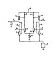
- the feedback differential sense amplifier consists of two current sense amplifiers T1 and T2 or T3 and T4, which are connected together as a differential amplifier.
- the input transistors T1 and T2 are an emitter-coupled pair of transistor switches with corresponding input lines 11 and 12.
- the transistor T1 is connected with its base to the input line 11, while its emitter electrode is connected to the emitter electrode of the transistor T2 and to a common current source 10 and its collector electrode to the Base electrode of a transistor T3 connected as an emitter follower and connected to a positive voltage source 15 via a resistor 13.
- the transistor T2 is not only connected via emitter coupling to the transistor T1 and to the current source 10, but is connected at its base electrode to the input line 12 and its collector electrode is at the base electrode of a transistor T4 connected as an emitter follower and via a resistor 14 to the positive voltage source 15 connected.
- the transistor T3 connected as an emitter follower is connected with its collector electrode to the voltage source 15 and its emitter electrode is connected with the output line 17 and is connected to the input line 11 via a resistor 19.
- the emitter electrode of transistor T3 is also connected to the base electrode of a latch transistor T5.
- the transistor T4 connected as an emitter follower is connected with its collector electrode to the voltage source 15 and coupled with its emitter electrode to an output line 18 and connected to the input line 12 via a resistor 20.
- the emitter electrode of transistor T4 is also coupled to the base of a second latch transistor T6.
- the locking transistor T5 is coupled with its collector electrode to the input sensing line 11 and is connected with its emitter electrode to a pulsed current source 16.
- the locking transistor T6 is connected with its collector electrode to the input line 12 and its emitter electrode is coupled to the emitter electrode of the transistor T5 and with the pulse-operated power source 16 connected.
- This sense amplifier works as follows: Differential input signals sensed on the input lines 11 and 12 are sensed by the input transistors T1 and T2 and emitted to the output lines 17 and 18 via transistors T3 and T4 connected as emitter followers.
- the feedback resistors 19 and 20 are selected so that the gain of the feedback amplifier is just sufficient to turn on the detector circuit by the voltage difference between the output lines 17 and 18 when a differential signal occurs on the input lines. For example, let's start with taken that the differential input signal is such that the input line 11 has a low potential and -ieie input line 12 has a higher potential.
- the potential of the base electrode of the transistor T1 is also lowered, so that the transistor T1 begins to switch off, as a result of which the current flowing through this transistor T1 drops.
- the base of the transistor T3 With the decrease in the current flowing through the transistor T1, the base of the transistor T3 becomes more positive, so that the transistor T3 turns on and thus raises the output line 17 and the base electrode of the locking transistor T5 to a higher potential.
- the input line 12 is brought to a higher potential, ie positive with respect to the input line 11, as a result of which the transistor T2 switches on and draws a higher current from the voltage source 15 via the resistor 14 and at the same time thus lowers the base voltage of the transistor T4 connected as an emitter follower .
- the potential on output line 18 and on the base of transistor T6 also decreases.
- this feedback effects an amplification of the input signals occurring on the input lines 11 and 12. If the current difference of the currents lying on the input lines 11 and 12 is 1 microampere, and if the current source is a current sink for 200 microampere, for example, as soon as the feedback locking circuit via the transistors T5 and T6 comes into operation, a differential input signal of obviously becomes 201 microamperes are fed to the base electrodes of the input transistors T1 and T2.
- the basic circuit of the feedback amplifier consisting of the transistors T1, T3 and T2, T4 inverts the input signal with respect to the associated output line, i. H. that when the input line 11 is negative, the output line 17 has a positive potential.
- the locking transistors T5 and T6 need not be cross-coupled, but should only be coupled directly to the corresponding input and output lines.
- the latch transistors T5 and T6 not only latch the input signal but also amplify it, so that the transistors T1 and T2 are kept even more in the operating state in which they were originally set by the incoming input signal.
- the input signal and the gain of the amplifier need not be large. If the locking transistors T5 and T6 hold themselves, then the current of the pulsed current source 16 is added to the signal and is therefore in phase. Because the size of the current supplied by the pulsed current source 16 is an independent parameter and is unrelated to the gain of the amplifier or the input signal, this current can be adjusted in itself so that the desired logic output signal is one of the gain of the amplifier or the amplitude of the input signal has independent output amplitude.
- latch transistors T5 and T6 provide the output potential and not the amplitude of the input signal by adding a pseudo signal to the input signal.
- this makes it possible to use an amplifier with a lower degree of amplification, which inherently has a larger bandwidth and less asymmetry.
- the pulsed current source is only used when the input transistors T1 and T2 are not inherently balanced. If all the transistors are matched to one another, then a normal current source can be used instead of the current source 16 operated in pulsed fashion.
- the invention requires a DC amplifier in which the output voltage amplitude differs only slightly from the input amplitude.
- inverting and non-inverting amplifiers can be used by simply adjusting the phase position at the base electrodes of T5, T6 by cross coupling or direct coupling accordingly.
Landscapes
- Physics & Mathematics (AREA)
- Nonlinear Science (AREA)
- Amplifiers (AREA)
- Manipulation Of Pulses (AREA)
- Static Random-Access Memory (AREA)
Applications Claiming Priority (2)
| Application Number | Priority Date | Filing Date | Title |
|---|---|---|---|
| US06/029,590 US4264832A (en) | 1979-04-12 | 1979-04-12 | Feedback amplifier |
| US29590 | 1979-04-12 |
Publications (2)
| Publication Number | Publication Date |
|---|---|
| EP0017730A1 true EP0017730A1 (fr) | 1980-10-29 |
| EP0017730B1 EP0017730B1 (fr) | 1983-02-16 |
Family
ID=21849831
Family Applications (1)
| Application Number | Title | Priority Date | Filing Date |
|---|---|---|---|
| EP80100857A Expired EP0017730B1 (fr) | 1979-04-12 | 1980-02-21 | Amplificateur différentiel contre-réactionné |
Country Status (5)
| Country | Link |
|---|---|
| US (1) | US4264832A (fr) |
| EP (1) | EP0017730B1 (fr) |
| JP (1) | JPS5843837B2 (fr) |
| DE (1) | DE3061954D1 (fr) |
| IT (1) | IT1150088B (fr) |
Cited By (2)
| Publication number | Priority date | Publication date | Assignee | Title |
|---|---|---|---|---|
| EP0082403A3 (fr) * | 1981-12-21 | 1984-07-04 | International Business Machines Corporation | Amplificateur transistorisé d'écriture/lecture destiné à une mémoire magnétique |
| EP0441200A3 (en) * | 1990-02-08 | 1993-05-26 | Texas Instruments Incorporated | Sense amplifier and method for sensing the outputs of static random access memory cells |
Families Citing this family (5)
| Publication number | Priority date | Publication date | Assignee | Title |
|---|---|---|---|---|
| US4547685A (en) * | 1983-10-21 | 1985-10-15 | Advanced Micro Devices, Inc. | Sense amplifier circuit for semiconductor memories |
| US4622475A (en) * | 1984-03-05 | 1986-11-11 | Tektronix, Inc. | Data storage element having input and output ports isolated from regenerative circuit |
| JPS6410339U (fr) * | 1987-07-03 | 1989-01-19 | ||
| US5182560A (en) * | 1989-12-22 | 1993-01-26 | Texas Instruments Incorporated | Analog-to-digital converter for high speed low power applications |
| GB2459865B (en) * | 2008-05-07 | 2011-03-16 | Wolfson Microelectronics Plc | Amplifier Circuit |
Citations (1)
| Publication number | Priority date | Publication date | Assignee | Title |
|---|---|---|---|---|
| DE2226471A1 (de) * | 1971-06-03 | 1973-01-25 | Motorola Inc | Differential-stromverstaerker |
Family Cites Families (4)
| Publication number | Priority date | Publication date | Assignee | Title |
|---|---|---|---|---|
| US3621301A (en) * | 1969-12-31 | 1971-11-16 | Ibm | Threshold-responsive regenerative latching circuit |
| US3745539A (en) * | 1972-03-20 | 1973-07-10 | Ibm | Latch type regenerative circuit for reading a dynamic memory cell |
| GB1401262A (en) * | 1973-02-23 | 1975-07-16 | Ibm | Data storage apparatus |
| DE2460146C3 (de) * | 1974-12-19 | 1981-11-05 | Ibm Deutschland Gmbh, 7000 Stuttgart | Bipolare Leseschaltung für integrierte Speichermatrix |
-
1979
- 1979-04-12 US US06/029,590 patent/US4264832A/en not_active Expired - Lifetime
-
1980
- 1980-02-21 EP EP80100857A patent/EP0017730B1/fr not_active Expired
- 1980-02-21 DE DE8080100857T patent/DE3061954D1/de not_active Expired
- 1980-03-07 IT IT20406/80A patent/IT1150088B/it active
- 1980-03-10 JP JP55029280A patent/JPS5843837B2/ja not_active Expired
Patent Citations (1)
| Publication number | Priority date | Publication date | Assignee | Title |
|---|---|---|---|---|
| DE2226471A1 (de) * | 1971-06-03 | 1973-01-25 | Motorola Inc | Differential-stromverstaerker |
Non-Patent Citations (4)
| Title |
|---|
| IBM TECHNICAL DISCLOSURE BULLETIN, Band 10, Nr. 5, Oktober 1967, Seiten 672-673 New York, U.S.A. P.D. BELLAMY et al.: "Nonsaturating, low source impedance, complementary driver" * Figur; Seite 672, Absatz 2 - Seite 673, Zeile 1 * * |
| IBM TECHNICAL DISCLOSURE BULLETIN, Band 12, Nr. 12, Mai 1970, Seite 2123 New York, U.S.A. N.M. DONOFRIO et al.: "Differential shunt feedback sense amplifier" * Figur * * |
| IBM TECHNICAL DISCLOSURE BULLETIN, Band 16, Nr. 5, Oktober 1973, Seiten 1600-16001 New York, U.S.A. P.R. EPLEY et al.: "Schmitt trigger circuit" * Seite 1600, Figur und Zeile 17 - Seite 1601 * * |
| IBM TECHNICAL DISCLOSURE BULLETIN, Band 19, Nr. 1, Juni 1976, Seite 137 New York, U.S.A. P. DEBORD et al.: "High-speed comparator" * Figur und zwei letzte Absatze * * |
Cited By (2)
| Publication number | Priority date | Publication date | Assignee | Title |
|---|---|---|---|---|
| EP0082403A3 (fr) * | 1981-12-21 | 1984-07-04 | International Business Machines Corporation | Amplificateur transistorisé d'écriture/lecture destiné à une mémoire magnétique |
| EP0441200A3 (en) * | 1990-02-08 | 1993-05-26 | Texas Instruments Incorporated | Sense amplifier and method for sensing the outputs of static random access memory cells |
Also Published As
| Publication number | Publication date |
|---|---|
| US4264832A (en) | 1981-04-28 |
| DE3061954D1 (en) | 1983-03-24 |
| JPS5843837B2 (ja) | 1983-09-29 |
| IT1150088B (it) | 1986-12-10 |
| JPS55138908A (en) | 1980-10-30 |
| IT8020406A0 (it) | 1980-03-07 |
| EP0017730B1 (fr) | 1983-02-16 |
Similar Documents
| Publication | Publication Date | Title |
|---|---|---|
| EP0096944B1 (fr) | Circuit avec plusieurs chemins de signaux formés par des composants actifs | |
| DE69210305T2 (de) | Mehrstufiger Differenzverstärker | |
| DE3120979A1 (de) | Spannungsvergleicher | |
| DE68928959T2 (de) | Logik-Schaltungsanordnungen | |
| DE2425218A1 (de) | Schaltkreis | |
| EP0529119A1 (fr) | Amplificateur intégré monolithique avec commande de gain | |
| DE69807592T2 (de) | Chopper-Komparator für Spannungen | |
| DE3012965C2 (fr) | ||
| DE3432510C2 (fr) | ||
| DE69424985T2 (de) | Transimpedanzverstärkerschaltung mit variablen Rückkopplungs- und Lastwiderstandsschaltungen | |
| DE2501288A1 (de) | Anordnung zum verstaerken elektrischer signale | |
| DE1812292C3 (de) | Schaltungsanordnung zur Verstärkungsregelung | |
| DE2213484C3 (de) | Hochfrequenter Breitbandverstärker | |
| EP0017730B1 (fr) | Amplificateur différentiel contre-réactionné | |
| DE3036764A1 (en) | Gain control circuit | |
| DE3310978C2 (de) | Verstärkerschaltung | |
| DE3602551C2 (de) | Operationsverstärker | |
| DE4209858C2 (de) | Transferleitwert-Verstärker | |
| DE2053888A1 (de) | Schaltungsanordnung zur Umformung bipolarer Eingangssignale in unipolare Signale | |
| DE69024711T2 (de) | Verstärkerschaltung | |
| DE2322466C3 (de) | Operationsverstärker | |
| DE3854047T2 (de) | Asymetrischer verstärker mit zwei eingängen. | |
| DE1116724B (de) | Leseverstaerker fuer Matrixspeicher | |
| DE1293860B (de) | Transistorbestueckter Differentialverstaerker mit drei in Kaskade geschalteten Verstaerkerstufen | |
| DE3109441A1 (de) | Operationsverstaerker mit erhoehter einschwinggeschwindigkeit |
Legal Events
| Date | Code | Title | Description |
|---|---|---|---|
| PUAI | Public reference made under article 153(3) epc to a published international application that has entered the european phase |
Free format text: ORIGINAL CODE: 0009012 |
|
| AK | Designated contracting states |
Designated state(s): DE FR GB NL SE |
|
| 17P | Request for examination filed |
Effective date: 19801203 |
|
| GRAA | (expected) grant |
Free format text: ORIGINAL CODE: 0009210 |
|
| AK | Designated contracting states |
Designated state(s): DE FR GB NL SE |
|
| PG25 | Lapsed in a contracting state [announced via postgrant information from national office to epo] |
Ref country code: NL Effective date: 19830216 |
|
| REF | Corresponds to: |
Ref document number: 3061954 Country of ref document: DE Date of ref document: 19830324 |
|
| ET | Fr: translation filed | ||
| NLV1 | Nl: lapsed or annulled due to failure to fulfill the requirements of art. 29p and 29m of the patents act | ||
| PGFP | Annual fee paid to national office [announced via postgrant information from national office to epo] |
Ref country code: SE Payment date: 19840331 Year of fee payment: 5 |
|
| PG25 | Lapsed in a contracting state [announced via postgrant information from national office to epo] |
Ref country code: SE Effective date: 19860222 |
|
| PGFP | Annual fee paid to national office [announced via postgrant information from national office to epo] |
Ref country code: GB Payment date: 19910118 Year of fee payment: 12 |
|
| PGFP | Annual fee paid to national office [announced via postgrant information from national office to epo] |
Ref country code: FR Payment date: 19910123 Year of fee payment: 12 |
|
| PGFP | Annual fee paid to national office [announced via postgrant information from national office to epo] |
Ref country code: DE Payment date: 19910204 Year of fee payment: 12 |
|
| PG25 | Lapsed in a contracting state [announced via postgrant information from national office to epo] |
Ref country code: GB Effective date: 19920221 |
|
| GBPC | Gb: european patent ceased through non-payment of renewal fee | ||
| PG25 | Lapsed in a contracting state [announced via postgrant information from national office to epo] |
Ref country code: FR Effective date: 19921030 |
|
| PG25 | Lapsed in a contracting state [announced via postgrant information from national office to epo] |
Ref country code: DE Effective date: 19921103 |
|
| REG | Reference to a national code |
Ref country code: FR Ref legal event code: ST |
|
| EUG | Se: european patent has lapsed |
Ref document number: 80100857.4 Effective date: 19861022 |
|
| PLBE | No opposition filed within time limit |
Free format text: ORIGINAL CODE: 0009261 |
|
| STAA | Information on the status of an ep patent application or granted ep patent |
Free format text: STATUS: NO OPPOSITION FILED WITHIN TIME LIMIT |