EP0019630B1 - Empfindlichkeitsschaltung für zwischenfrequenz - Google Patents
Empfindlichkeitsschaltung für zwischenfrequenz Download PDFInfo
- Publication number
- EP0019630B1 EP0019630B1 EP79900437A EP79900437A EP0019630B1 EP 0019630 B1 EP0019630 B1 EP 0019630B1 EP 79900437 A EP79900437 A EP 79900437A EP 79900437 A EP79900437 A EP 79900437A EP 0019630 B1 EP0019630 B1 EP 0019630B1
- Authority
- EP
- European Patent Office
- Prior art keywords
- circuit
- output
- voltage
- intermediate frequency
- detection
- Prior art date
- Legal status (The legal status is an assumption and is not a legal conclusion. Google has not performed a legal analysis and makes no representation as to the accuracy of the status listed.)
- Expired
Links
- 238000001514 detection method Methods 0.000 claims description 40
- 238000009877 rendering Methods 0.000 claims 1
- 230000007257 malfunction Effects 0.000 abstract 1
- 239000003990 capacitor Substances 0.000 description 11
- 238000010586 diagram Methods 0.000 description 4
- 230000008901 benefit Effects 0.000 description 2
- 230000008859 change Effects 0.000 description 2
- 230000007423 decrease Effects 0.000 description 2
- 230000004048 modification Effects 0.000 description 2
- 238000012986 modification Methods 0.000 description 2
- 238000010408 sweeping Methods 0.000 description 2
- 230000002159 abnormal effect Effects 0.000 description 1
- 230000009471 action Effects 0.000 description 1
- 238000006243 chemical reaction Methods 0.000 description 1
- 230000008878 coupling Effects 0.000 description 1
- 238000010168 coupling process Methods 0.000 description 1
- 238000005859 coupling reaction Methods 0.000 description 1
- 230000001419 dependent effect Effects 0.000 description 1
- 238000009499 grossing Methods 0.000 description 1
- 230000004044 response Effects 0.000 description 1
- 238000007493 shaping process Methods 0.000 description 1
Images



Classifications
-
- H—ELECTRICITY
- H03—ELECTRONIC CIRCUITRY
- H03J—TUNING RESONANT CIRCUITS; SELECTING RESONANT CIRCUITS
- H03J7/00—Automatic frequency control; Automatic scanning over a band of frequencies
- H03J7/18—Automatic scanning over a band of frequencies
Definitions
- This invention concerns an intermediate frequency sensing or detection circuit of a radio receiver which is ensured to generate an output indicative of the reception for broadcasting waves with no erroneous operations caused by spurious signals or the like.
- Electronically tuning type radio receivers capable of automatic search channel selection recognize the tuning to a broadcasting wave when an intermediate frequency stage generates an output, interrupt then the frequency sweeping and enter into a receiving state.
- the intermediate frequency stage generates its output by the reception not only of broadcasting waves but also of harmonic waves (spurious signals) thereof to interrupt the channel selection operation.
- a circuit for taking out the intermediate frequency output for channel selection (hereinafter referred to as IF detection circuit) is, desirably, designed so that it produces no output upon reception of the harmonic waves or noises.
- the IF detection circuit is adapted to monitor the output from the intermediate frequency stage at a certain threshold level and generates an output when the intermediate frequency output exceeds this level, this system results in a problem that a frequency width exceeding the threshold level changes depending on the level of the input signals. If the frequency width becomes broader exact tuning is of course made difficult. It is, accordingly, desired for the IF detection circuit to output a narrow width pulse at an exact tuning point.
- an object of this invention to provide an IF detection circuit capable of satisfying the aforesaid requirements with a simple circuit structure.
- a first circuit for producing a signal indicating the output level of an intermediate frequency stage of superheterodyne type radio receiver a second circuit for producing a signal indicating the output level of a high frequency stage of the above receiver and a logic circuit to which the outputs from the above first and second circuits are inputted, and the above logic circuit generates a signal indicating the reception of a broadcasting wave when the intermediate frequency output is high and the high frequency output is low.
- the signal indicating the output level of the intermediate frequency stage is, simply, obtained from an AGC circuit. Since a time constant in the AGC circuit is relatively great, particularly, in an AM receiver in this case, a problem arises that the signal indicating the output level of the intermediate frequency can not be obtained rapidly.
- a switching circuit is provided, which decreases the time constant of the AGC circuit during channel selection in this invention.
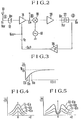
- an antenna 10 a tuning circuit 12, a high frequency amplifier 14, a frequency mixer 16, a local oscillator 18, an intermediate frequency amplifier 20, an intermediate frequency transformer 22, a detector 24 and an AGC circuit 26, which constitute a well known tuner section in a superheterodyne type radio receiver.
- Reference numeral 30 represents an IF detection circuit according to this invention, which consists of detectors 32, 34 for each of the levels of intermediate frequency and high frequency and a logic circuit 36.
- the intermediate frequency transformer 22 produces an IF output. If the IF output is used as it is for the interruption of the frequency sweeping, erroneous operation may possibly result as described previously since the IF output is generated by the reception not only of a broadcasting wave but also of its harmonic waves, as well as noises contained in a broad band area, that is, in the same frequency range as that of the broadcasting wave.
- the IF output if caused by the harmonic waves, has a feature that the output Em produced then from the high frequency stage is abnormally high. This has been specifically described in Japanese Patent Application No. 99766/1977 (Patent No.
- the gain of the high frequency stage is controlled so that the intermediate frequency output becomes approximately constant in an AGC-controlled receiver. Accordingly, assuming the ratio of the amplitude of the harmonic wave to the fundamental wave as 1/K (where K > 1), the gain of the high frequency stage if tuned to the harmonic wave becomes K times as great as the gain when tuned to the fundamental wave. Since the output Em from the high frequency stage also contains the fundamental wave, the fundamental wave is increased by the factor of K as compared with the usual case to render the output Em abnormally high. It is the same when the tuner responds to the noises. Erroneous detection for the broadcasting wave reception caused by the harmonic waves and broad band noises can be inhibited simply by utilizing the above phenomenon.
- the logic circuit 36 is used for this purpose and it has a logic function of generating an IF detection output DI where an IF output E o is high thus causing the intermediate frequency level detector 32 to produce an output and a high frequency stage output Em is low thus causing the high frequency level detector 34 to produce no output, and generating no such IF detection output DI where the detector 32 produces no output or when the detector 32 produces an output but the detector 34 also produces an output.
- the voltage of the AGC circuit may, advantageously be utilized since it has a value depending on the IF output E o .
- the voltage relations in each of the sections are to be detailed with respect to the later case.
- is represented by the equation (1) for the single tuning and by the equation (2) for the double tuning: wherein f o is a center (resonance point) frequency and Q is a quality factor of the resonance circuit.
- f o is a center (resonance point) frequency
- Q is a quality factor of the resonance circuit.
- the tuner output voltage E o to a signal detuned by ⁇ f from the tuning frequency of the tuner is represented by the following equation: where Q RF and Q IF represent Q for the coils in each of the high frequency stage and the intermediate frequency stage respectively and f oRF and f oIF represent center frequencies of the same.
- the gain G 1max is represented as: where R is a conversion constant, the following equation was obtained from the equations (3) and (4).
- the following equation is obtained:
- Fig. 3-Fig. 5 shows the relation of the IF output E o relative to the input voltage Ei
- Fig. 4 and Fig. 5 show the relations of the output voltages E o and Em relative to the detuning degree ⁇ f.
- the AGC voltage waveforms are as shown in Fig. 6. As can be seen from Fig.
- the above difference in the width W 2 , W 3 means the difference in the detection frequency width, which causes a difficulty in the exact tuning.
- detection signal is generated also for the spurious signals.
- the width of the detection signal is rendered constant by utilizing the output Em from the high frequency stage as well in this invention.
- (a) represents the IF detection signals DO 2 , D0 3 and the high frequency detection signals DM 1 -DM 3 relative to' the frequency deviation ⁇ f and (b) represents the IF detection outputs DI 2 , DI 3 obtained through the above logic function.
- outputs are present at the reception of broadcasting waves but absent at the reception of the spurious signals and the broad band noises, and IF detection signal outputs with an approximately constant frequency width are obtainable by obtaining the level information from the AGC voltage V AGC and the frequency information from the high frequency stage output.
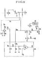
- FIG. 9 Specific embodiments of this invention are to be shown in Fig. 9 and Fig. 10.
- Fig. 9 are shown an amplifying transistor Tr 3 for the high frequency stage 14, a transistor Tr 4 for the mixer 16 and a transistor Tr 5 for the intermediate frequency stage 20.
- the output Em from the high frequency stage is taken out from the input terminal of the mixer 16, amplified through an amplifying circuit consisting of a transistor Tr 2 , resistors R 2 , R 3 and a capacitor C 3 and detected by a capacitor C 2 and a detecting diode D, to produce a DC voltage V EM corresponding to the high frequency stage output Em.
- a capacitor C 6 , a diode D 4 , a'resistor R 4 and a capacitor C 5 form an AGC circuit, which produces the foregoing AGC voltage V AGC .
- Diodes D 2 , D 3 and a resistor R 1 compare the voltage V AGC with the voltage V EM to take out a higher voltage of them.
- a capacitor C 1 is for smoothing use.
- a comparator 38 has applied to one of its terminals a reference voltage Vs for determining the threshold level and to the other of its terminals the voltage V AGC or V EM
- a voltage V AGC -V D3 (V D3 is a forward voltage drop across the diode D 3 ) is usually applied to the input terminal of the comparator 38. Since the voltage is higher than the reference voltage Vs, the comparator 38 produces no output. If the IF output E o becomes higher by the reception of the broadcasting waves or the likes, the voltage V AGC -V D3 goes lower than Vs causing the comparators 38 to generate the output DI.
- the output is, however, generated only when the output Em is low, and the comparator 38 generates no output DI where the high frequency stage output Em is high such as by the input of the spurious signals or the broad band noises and ⁇ f detuning since the voltage V EM -V D2 (V D2 is a voltage drop across the diode D 2 ) is inputted to the comparator 38 and it is not lower than the reference voltage Vs.
- a transistor Tr is used for switching the time constant in the AGC circuit, which is turned ON and OFF upon input to its base of a control signal such as a signal SG that takes an H (high) level during reception and turns to an L (low) level during searching, and connects the capacitor C 4 in parallel with the capacitor C 3 in the ON state to increase the time constant and, while on the other hand, disconnects the capacitor C 4 from the capacitor C 3 in the OFF state to decrease the time constant.
- a control signal such as a signal SG that takes an H (high) level during reception and turns to an L (low) level during searching
- the logic circuit 36 surrounded by a dotted line in Fig. 9 may alternatively be formed as shown in Fig. 10.
- a diode D 5 , resistors R 6 , R 7 and a capacitor C 7 prepare a voltage Va formed by subtracting from the reference voltage Vs a DC voltage corresponding to the level of the output Em, and diodes D 6 , D,, and a resistor R s prepare a voltage Vb usually at a value of V AGC -V D7 and restricted not to be lower than V S -V D6 .
- V D6 , V D7 represent forward voltage drops across the diodes D e , D 7 respectively.
- the IF detection operation is described below.
- the circuit is provided with a diode D6, resistor R s and is applied with voltage Vs as illustrated.
- the reasons are as follows. Since the state in which the voltage Va is lower than the voltage Vs to some extent can be considered abnormal, it is desired in such a case to avoid the generation of the IF detection how the intermediate frequency output is high. Then, the voltage Vb is restricted so as not to be lower than V S -V D6 , by which the IF detection output is kept from generation if the high frequency stage output Em is abnormally high.
Landscapes
- Circuits Of Receivers In General (AREA)
- Superheterodyne Receivers (AREA)
- Channel Selection Circuits, Automatic Tuning Circuits (AREA)
- Control Of Amplification And Gain Control (AREA)
- Input Circuits Of Receivers And Coupling Of Receivers And Audio Equipment (AREA)
- Transmitters (AREA)
Claims (4)
1. Zwischenfrequenz-Demodulatorschaltung zur Erzeugung eines Zwischenfrequenz-Demodulationsausgangs, welcher den Empfang einer Rundfunkwelle in einem Superheterodyn-Radioempfänger anzeigt, dadurch gekennzeichnet, dass die Schaltung eine erste Schaltung (32) zur Erzeugung eines Signals, das den Ausgangspegel einer Zwischenfrequenzstufe (20, 22) in dem Radioempf- äger anzeigt, aufweist, sowie eine zweite Schaltung (34) zur Erzeugung eines Signals, welches den Ausgangspegel einer Hochfrequenzstufe (14) in dem Radioempfänger anzeigt, und eine logische Schaltung (36), an deren Eingänge die Ausgänge der ersten und der zweiten Schaltung angelegt sind, und die den Demodulationsausgang (DI), wenn der Ausgang der Zwischenfrequenzstufe hoch und der Ausgang der Hochfrequenzstufe niedrig ist, erzeugt.
2. Zwischenfrequenz-Demodulatorschaltung nach Anspruch 1, dadurch gekennzeichnet, dass die erste Schaltung aus einer Schaltung (R4, C5, C6, D4) zur Bildung einer AGC-Spannung des Empfängers besteht, die zweite Schaltung aus einer Schaltung (TR2, C2, D1) zur Herausführung und Demodulation des Ausgangs aus dem Hochfrequenzverstärker besteht und dass die logische Schaltung (36) zur Erzeugung des Demodulationsausgangs aus einem Komparator (38) besteht an dessen einem Eingangsanschluss eine Referenzspannung (VS) angelegt ist, sowie aus einer Schaltung (D2, D3, R1) zum Anlegen des höheren der beiden Ausgänge aus der ersten und der zweiten Schaltung an den anderen Eingangsanschluss des Komparators.
3. Zwischenfrequenz-Demodulatorschaltung nach Anspruch 1, dadurch gekennzeichnet, dass die erste Schaltung aus einer Schaltung (R4, C5, C6, D4) zum Herausnehmen einer AGC-Spannung des Empfängers besteht, dass die zweite Schaltung aus einer Schaltung (Tr2, C2, D1) zum Herausnehmen und Demodulieren des Ausgangs aus dem Hochfrequenzverstärker besteht, und dass die logische Schaltung (36) zur Erzeugung des Demodulationsausgangs aus einem Komparator (38) besteht, an dessen einem Eingangsanschluss (Vb) die Ausgangsspannung (Vagc) von der ersten Schaltung angelegt, ist, sowie aus einer Schaltung, die an den anderen Eingangsanschluss (Va) des Komparators eine Spannung anlegt, die durch Subtraktion der Ausgangsspannung (VEM) der zweiten Schaltung von einer Referenzspannung (Vs) gebildet ist.
4. Zwischenfrequenz-Demodulatorschaltung nach Anspruch 2 oder 3, dadurch gekennzeichnet, dass die erste Schaltung zum Herausführen der AGC-Spannung des Empfängers eine Umschalt-Schaltung (TR1, R5, C4, C5) umfasst, welche die Zeitkonstante in der AGC-Schaltung des Empfängers während der Suchkanalauswahl kleiner macht als während des Empfanges.
Applications Claiming Priority (2)
| Application Number | Priority Date | Filing Date | Title |
|---|---|---|---|
| JP53045149A JPS5854682B2 (ja) | 1978-04-17 | 1978-04-17 | 中間周波検出回路 |
| JP45149/78 | 1978-04-17 |
Publications (3)
| Publication Number | Publication Date |
|---|---|
| EP0019630A4 EP0019630A4 (de) | 1980-10-09 |
| EP0019630A1 EP0019630A1 (de) | 1980-12-10 |
| EP0019630B1 true EP0019630B1 (de) | 1983-05-11 |
Family
ID=12711215
Family Applications (1)
| Application Number | Title | Priority Date | Filing Date |
|---|---|---|---|
| EP79900437A Expired EP0019630B1 (de) | 1978-04-17 | 1979-11-19 | Empfindlichkeitsschaltung für zwischenfrequenz |
Country Status (10)
| Country | Link |
|---|---|
| US (1) | US4403349A (de) |
| EP (1) | EP0019630B1 (de) |
| JP (1) | JPS5854682B2 (de) |
| CA (1) | CA1142596A (de) |
| CH (1) | CH647630A5 (de) |
| DE (1) | DE2947101C2 (de) |
| GB (1) | GB2046542B (de) |
| NL (1) | NL185124C (de) |
| SE (1) | SE418439B (de) |
| WO (1) | WO1979000937A1 (de) |
Cited By (1)
| Publication number | Priority date | Publication date | Assignee | Title |
|---|---|---|---|---|
| US10693570B2 (en) | 2018-08-20 | 2020-06-23 | Rohde & Schwarz Gmbh & Co. Kg | Device and method of analyzing a radio frequency signal |
Families Citing this family (1)
| Publication number | Priority date | Publication date | Assignee | Title |
|---|---|---|---|---|
| JP3462772B2 (ja) * | 1998-11-30 | 2003-11-05 | 三洋電機株式会社 | ラジオ受信機 |
Family Cites Families (10)
| Publication number | Priority date | Publication date | Assignee | Title |
|---|---|---|---|---|
| NL76666C (de) * | 1949-07-22 | |||
| US2652486A (en) * | 1949-07-22 | 1953-09-15 | Gen Motors Corp | Signal seeking tuner |
| US2764675A (en) * | 1950-01-28 | 1956-09-25 | Gen Motors Corp | Signal actuated tuner selective over noise level |
| US2843734A (en) * | 1956-02-29 | 1958-07-15 | Bendix Aviat Corp | Signal seeking radio receiver |
| US3569840A (en) * | 1968-10-04 | 1971-03-09 | Collins Radio Co Of Canada Ltd | Carrier squelch scheme |
| JPS5119286A (ja) * | 1974-08-07 | 1976-02-16 | Victor Company Of Japan | Jidoseigyohoshiki |
| US3947771A (en) * | 1975-02-21 | 1976-03-30 | General Motors Corporation | Keyed classical AGC system |
| DE2522382A1 (de) * | 1975-05-21 | 1976-12-02 | Blaupunkt Werke Gmbh | Schaltungsanordnung zum unterdruecken von stoerungen in einem rundfunkempfaenger |
| JPS5317212A (en) * | 1976-07-31 | 1978-02-17 | Torio Kk | Device for eliminating intermodulation disturbance of superheterodyne receiver |
| DE2755221C2 (de) * | 1977-12-10 | 1985-05-30 | Felten & Guilleaume Fernmeldeanlagen GmbH, 8500 Nürnberg | Verfahren zur selbsttätigen Überwachung der HF-Empfindlichkeit und des NF-Ausgangspegels eines Funkempfängers und Schaltungsanordnung zur Durchführung des Verfahrens |
-
1978
- 1978-04-17 JP JP53045149A patent/JPS5854682B2/ja not_active Expired
-
1979
- 1979-04-04 WO PCT/JP1979/000083 patent/WO1979000937A1/ja not_active Ceased
- 1979-04-04 US US06/179,288 patent/US4403349A/en not_active Expired - Lifetime
- 1979-04-04 CH CH11175/79A patent/CH647630A5/de not_active IP Right Cessation
- 1979-04-04 GB GB8013838A patent/GB2046542B/en not_active Expired
- 1979-04-04 DE DE19792947101 patent/DE2947101C2/de not_active Expired
- 1979-04-05 NL NLAANVRAGE7902692,A patent/NL185124C/xx not_active IP Right Cessation
- 1979-04-12 CA CA000325447A patent/CA1142596A/en not_active Expired
- 1979-11-19 EP EP79900437A patent/EP0019630B1/de not_active Expired
-
1980
- 1980-05-12 SE SE8003557A patent/SE418439B/sv not_active IP Right Cessation
Cited By (1)
| Publication number | Priority date | Publication date | Assignee | Title |
|---|---|---|---|---|
| US10693570B2 (en) | 2018-08-20 | 2020-06-23 | Rohde & Schwarz Gmbh & Co. Kg | Device and method of analyzing a radio frequency signal |
Also Published As
| Publication number | Publication date |
|---|---|
| SE418439B (sv) | 1981-05-25 |
| CA1142596A (en) | 1983-03-08 |
| GB2046542B (en) | 1982-10-20 |
| DE2947101T1 (de) | 1980-11-27 |
| US4403349A (en) | 1983-09-06 |
| WO1979000937A1 (fr) | 1979-11-15 |
| NL185124B (nl) | 1989-08-16 |
| CH647630A5 (de) | 1985-01-31 |
| JPS5854682B2 (ja) | 1983-12-06 |
| EP0019630A4 (de) | 1980-10-09 |
| EP0019630A1 (de) | 1980-12-10 |
| JPS54137214A (en) | 1979-10-24 |
| NL185124C (nl) | 1990-01-16 |
| NL7902692A (nl) | 1979-10-19 |
| SE8003557L (sv) | 1980-05-12 |
| DE2947101C2 (de) | 1986-06-12 |
| GB2046542A (en) | 1980-11-12 |
Similar Documents
| Publication | Publication Date | Title |
|---|---|---|
| EP0597905B1 (de) | Intermodulationssteuervorrichtung für einen Rundfunkempfänger | |
| CA1051567A (en) | Tuning system for am/fm receivers | |
| US4580285A (en) | Scanning AM radio with discriminator-driven-scan-stop-circuit | |
| US3072849A (en) | Radio receiver having voltage-controlled resonant circuit coupling means between stages | |
| US3611152A (en) | Stabilized automatic tuning receiver | |
| KR970004618B1 (ko) | 자동 탐색 튜너 | |
| KR0156938B1 (ko) | 자동 선국 회로에 있어서 신호 강도의 피크 검출 회로 | |
| KR970031405A (ko) | 라디오 수신기(Radio Receiver) | |
| EP0060845B1 (de) | Mechanische abstimmvorrichtung mit schaltungsanordnung zur beseitigung der mikrophonie | |
| US4403349A (en) | Intermediate frequency detection circuit | |
| US5487177A (en) | FM receiver comprising a circuit arrangement for determining the field strength of FM transmitters | |
| US4228546A (en) | AM Radio receiver | |
| US3018369A (en) | Transistorized direction finder receiver having a local audio signal modulated on the mixer | |
| US6356302B1 (en) | Apparatus for measuring S/N ratio of composite video signal | |
| US4228540A (en) | Radio receiver | |
| US6215829B1 (en) | Apparatus for selectively receiving carrier wave signals | |
| JPH048675Y2 (de) | ||
| US4499605A (en) | FM-Receiver using a ratio detector with silicon diodes | |
| KR830000365B1 (ko) | Rf 신호 수신기의 중심 주파수 동조 시스템 | |
| US4797636A (en) | Radio receiver | |
| KR960013786B1 (ko) | 라디오 채널 자동 탐색 장치 및 방법 | |
| US4530005A (en) | AFC circuit for television tuner | |
| JPS5818345Y2 (ja) | 受信機 | |
| US3405364A (en) | Reflex quenched superregenerative detector | |
| JPS6143319Y2 (de) |
Legal Events
| Date | Code | Title | Description |
|---|---|---|---|
| PUAI | Public reference made under article 153(3) epc to a published international application that has entered the european phase |
Free format text: ORIGINAL CODE: 0009012 |
|
| 17P | Request for examination filed | ||
| AK | Designated contracting states |
Designated state(s): FR |
|
| GRAA | (expected) grant |
Free format text: ORIGINAL CODE: 0009210 |
|
| AK | Designated contracting states |
Designated state(s): FR |
|
| ET | Fr: translation filed | ||
| PLBE | No opposition filed within time limit |
Free format text: ORIGINAL CODE: 0009261 |
|
| STAA | Information on the status of an ep patent application or granted ep patent |
Free format text: STATUS: NO OPPOSITION FILED WITHIN TIME LIMIT |
|
| 26N | No opposition filed | ||
| PGFP | Annual fee paid to national office [announced via postgrant information from national office to epo] |
Ref country code: FR Payment date: 19980306 Year of fee payment: 20 |