EP0020982A2 - Verfahren und Apparat zum Ausrichten eines Plättchens in eine gewünschte Position auf einem Arbeitsplatz - Google Patents
Verfahren und Apparat zum Ausrichten eines Plättchens in eine gewünschte Position auf einem Arbeitsplatz Download PDFInfo
- Publication number
- EP0020982A2 EP0020982A2 EP80102578A EP80102578A EP0020982A2 EP 0020982 A2 EP0020982 A2 EP 0020982A2 EP 80102578 A EP80102578 A EP 80102578A EP 80102578 A EP80102578 A EP 80102578A EP 0020982 A2 EP0020982 A2 EP 0020982A2
- Authority
- EP
- European Patent Office
- Prior art keywords
- wafer
- registration
- sense means
- edge
- flat
- Prior art date
- Legal status (The legal status is an assumption and is not a legal conclusion. Google has not performed a legal analysis and makes no representation as to the accuracy of the status listed.)
- Granted
Links
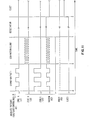
Images


Classifications
-
- H—ELECTRICITY
- H10—SEMICONDUCTOR DEVICES; ELECTRIC SOLID-STATE DEVICES NOT OTHERWISE PROVIDED FOR
- H10P—GENERIC PROCESSES OR APPARATUS FOR THE MANUFACTURE OR TREATMENT OF DEVICES COVERED BY CLASS H10
- H10P72/00—Handling or holding of wafers, substrates or devices during manufacture or treatment thereof
- H10P72/30—Handling or holding of wafers, substrates or devices during manufacture or treatment thereof for conveying, e.g. between different workstations
- H10P72/36—Handling or holding of wafers, substrates or devices during manufacture or treatment thereof for conveying, e.g. between different workstations using air tracks
- H10P72/3602—Handling or holding of wafers, substrates or devices during manufacture or treatment thereof for conveying, e.g. between different workstations using air tracks with angular orientation of the workpieces
Definitions
- This invention relates to an apparatus and method for orienting wafers or the like in a desired rotative position at a work station.
- U.S. Patent 3,890,508 discloses an apparatus for aligning a wafer having one flat registration edge.
- the apparatus comprises two registration blocks providing orthogonally arranged straight registration surfaces. Vacuum sense ports are disposed adjacent one of the registration surfaces. A pair of photocells are so disposed as to be outboard of the wafer periphery except when the wafer is aligned in a desired position defined by contact with a specific one of the straight registration surfaces.
- the wafer is rotated at a relatively fast rate until both photocells are uncovered; whereupon rotation rate is reduced.
- U.S. Patent 3,930,684 likewise discloses an apparatus for prealigning a wafer in a desired position using a fast, then a slower, rate of rotation in one direction.
- this apparatus if a wafer overshoots the proper pre-alignment position, pressure fluid pulses are again initiated to again rapidly, and then more slowly, rotate the wafer for another try at the proper pre-alignment position in which both electro-optical sensors are exposed substantially equal degrees to a light source.
- apparatus for orienting a substantially flat wafer having a flat registration edge
- said apparatus includes means providing a flat surface for supporting the wafer and providing a plurality of fluid jet ports, means extending upwardly from said flat surface and providing two registration surfaces, sense means associated with each of said registration surfaces, means for advancing the wafer toward contact with said registration surfaces, and means controlled by the conditioning of one of said sense means for controlling selective supply of fluid to said jet ports, means for rotating the wafer in one direction until a particular one of said sense means associated with a predetermined one of said registration surfaces is activated and means for rotating the wafer in the opposite direction until sense means in both registration surfaces are concurrently activated for causing wafer motion to be terminated, thereby to prevent overshoot and ensure precision registration of the wafer flat registration edge adjacent said predetermined registration surface.
- a method for orienting a substantially flat wafer or the like in a precise position defined by registration of a substantially flat edge of the wafer with one of two registration surfaces extending upwardly from a flat-surface of a support table characterised in that the method comprises the steps of providing sense means associated with each of said registration surfaces, advancing the wafer toward contact with said surfaces thereby conditioning one of said sense means, controlling selectively supply of fluid to jet ports provided in said support table, rotating the wafer in one direction by supplying fluid to one set of said jet ports until the sense means associated with a predetermined one of said surfaces is activated by contact of said edge portion therewith and thereafter rotating the wafer in.the opposite direction by supplying fluid to different set of said jet ports until the sense means associated with both of said surfaces are concurrently activated causing wafer motion to be terminated and thereby ensuring precision registration of the wafer flat registration edge adjacent said predetermined registration surface.
- the apparatus embodying the invention is adapted to orient, in a desired position, a substantially flat work piece, such as a wafer 10 of garnet material.
- a substantially flat work piece such as a wafer 10 of garnet material.
- wafer 10 is generally circular except for two generally flat, orthogonally related registration edges 11, 12 of unequal length.
- the apparatus embodying the invention comprises a support table 13, preferably of tool steel, having a wafer-supporting surface 14 that is lapped flat except for a series of concentric grooves 15 to which vacuum can be supplied via respective vacuum ports 16.
- Surface 14 is divided into three zones A, B and C.
- Block 17 which is disposed adjacent zone A, has a registration surface 19 with a double taper.
- a double taper At the apex of this double taper is a flat, metal strip-like valve element 20 that is inset in a sense port 21 and biased to project slightly (e.g., about .001") forwardly of the tapered surface 19.
- Block 18 is disposed adjacent zone B. It has a rectilinear non-tapered registration surface 22.
- Two flat metal strip-like valve elements 23, 24 (identical with valve element 20) are inset in respective sense ports 25, 26 and each biased to project slightly (also about .001") forwardly of the straight registration surface 22, as illustrated in FIGS. 8 and 9.
- the valve elements 20, 23 and 24 constitute movable sense elements that are moved when contacted by the periphery of the wafer 10, to cause sense signals to be generated in the manner hereinafter described.
- Adjacent zone C of the supporting surface 14 is an index block 27 that is provided with a set of directional jet ports 28.
- Other sets of directional jet ports 29, 30 and 31 are also provided in zones A and C, respectively.
- the jet ports 28-31 are activated to direct air at an angle of approximately 30° to the horizontal against the undersurface of wafer 10. This may be controlled as illustrated in FIG. 7, wherein air under pressure is supplied from a source 32 via a series of regulator valves 33-36 to respective solenoids 37-40. These solenoids are operative in conventional manner to control supply of air (preferably at the frequencies and amplitudes indicated in the timing diagram of FIG. 11.
- solenoids 37 and 39 operate to provide a series of low frequency pulses to ports 29 and 31 in zones A and C to cause the wafer to rotate clockwise at a fast rate.
- Solenoid 38 operates to provide a series of high frequency pulses to ports 30 in zone B to cause the wafer to rotate counterclockwise at a slow rate.
- Solenoid 40 operates to provide a continuous stream of air at a predetermined amplitude to ports 28 in index block 27.
- air is supplied from the respective solenoid 37-39 via respective manifolds such as 37a, 38a, 39a, (FIG. 1), with 39a being more clearly illustrated in FIG. 7.
- This figure also shows a vacuum manifold 41 via which vacuum is applied to the vacuum ports 16 and grooves 15 as a series of pulses under control of a solenoid 42 connected via a regulator valve 43 to a vacuum source 44.
- each sense means preferably includes, in addition to a strip-like valve element like 23, an electro-pneumatic switch device 45 comprising a bellows 46 and an electrical contact member 47.
- an electro-pneumatic switch device 45 comprising a bellows 46 and an electrical contact member 47.
- port 25 will be progressively restricted.
- absolute pressure in chamber 48 drops due to the increasingly effective influence of vacuum source 44, air at atmospheric pressure acting on the interior of bellows 46 will cause it to progressively elongate until it makes electrical contact with member 47 and thus causes an electrical signal to be supplied to solenoid control device 49.
- valve element 20 each of the valve elements 20, 23 and 24 operates in the manner just described in connection with valve element 23; and that solenoid control device 49-controls selective and concurrent operation of the respective solenoids 37-40 and 42.
- Solenoids 37-40 and 42 will now start to operate sequentially and/or concurrently to provide pulses of air or vacuum or a continuous stream of air, as depicted in the timing diagram of FIG. 11.
- a continuous stream of pressurized air supplied via index ports 28 will initially act on the under surface of wafer 10 for driving the wafer generally rectilinearly in the direction of arrows 50 toward registration surfaces 19, 22.
- solenoid control device 49 will become conditioned as shown at time W (FIG. 11). Pressurized air will thereupon be supplied as pulses via directional jet ports 29 and 31 to rotate wafer 10 clockwise at a relatively fast rate.
- the pressure of air supplied to ports 29 in zone A of surface 14 is, however, less (preferably about one-half) that supplied to ports 31 in zone C to cause the part of wafer 10 nearest the registration surfaces 19, 22 to be tilted downwardly towards support surface 14 to ensure that the wafer will not tend to ride upwardly along the registration surfaces, thereby to ensure proper operation of the sensing valve elements 20, 23, 24.
- Wafer 10 will continue to rotate clockwise through the position illustrated in FIG. 4 (in which longer wafer edge 11 contacts valve element 20) until said long edge attains the position illustrated in FIG. 5, in which it contacts and activates valve element 23.
- solenoid control device 49 will be operated to cause solenoid 38 to supply pressure fluid, as a series of short pulses, via jets 30 in zone B to the undersurface of wafer 10 to impart to it a slow counterclockwise motion. Jet 30a will gently keep the long edge 11 against valve element 23 and short edge 12 against valve element 20, while jet 30b will push wafer edge 11 toward valve element 24.
- valve elements 20, 23, 24 will be activated concurrently.
- wafer 10 will be in precise registered position.
- solenoid control device 49 will cause solenoids 37, 38, 39 and 40 to terminate supply of pressure fluid to jet ports 29, 30 and 31 in zones A, B and C and supply vacuum continuously via manifold 41 to hold the wafer in precise registered position so that a desired work operation may be performed thereon.
- pressure fluid is supplied under control of solenoid control device 49 from air source 32 to directional jet ports 51 via a manifold 51a and a solenoid (not shown) to eject the wafer from the work station in a preferred direction, such as that shown by arrows 52.
- the ports 28 are so located as to be outside the circumference of wafer 10 when it achieves its final registered position at time Y. This enables the wafer to settle down on surface 14 while the air from ports 28 acts on the edge (rather than the underside) of the wafer to hold the wafer registered.
- valve elements 23 and 24 are separated by a distance d (FIG. 1) which is less than the length of long edge 11 of wafer 10 but greater than the length of short edge 12. This is to ensure that valve element 23 will be activated only by the trailing part of long edge 11, and that the curved periphery and short edge 12 will not contact and hence cannot activate valve element 23.
- the surface 19 of registration block 17 has a double taper, as shown in FIG. 1. This is to ensure that in the event of non- orthogonality between the long and short edges 11, 12 neither the leading or trailing part of the short edge 12 can cause excessive separation between valve element 20 and the short edge.
- each edge 11, 12 will not be completely straight or flat, but will have irregularities due to rounding, chamfering, crumbling, or chipping. Therefore, the strip-like valve elements 20, 23, 24 have a width sufficient to span such irregularities to therefore average the irregularities and imperfections in the surface of edges 11, 12. This will ensure that the same part of edge 11 always contacts the valve elements 23, 24.
- the apparatus herein described is especially suited for use in orienting garnet wafers having two flat, generally orthogonally arranged registration edges of different length.
- the apparatus will register with the longer of said edges adjacent a specific registration surface irrespective of imperfections in or variations in angularity of the short flat registration edge with respect to the longer edge.
- the apparatus may be used, however, where the wafer has only one flat registration edge, provided such edge is longer than the dimension d between sensing valve elements 23, 24.
- valve element 20 is so disposed as to be activated by either the periphery of wafer 10 (whether it be the curved portion between flat registration edges or the registration edges themselves). This results from the fact that valve element 20 is disposed on a radial line from the wafer 10 as registered, whereas valve elements 23, 24 are . spaced apart to prevent their being contacted by a curved peripheral surface or even the short flat edge 12.
Landscapes
- Container, Conveyance, Adherence, Positioning, Of Wafer (AREA)
Applications Claiming Priority (2)
| Application Number | Priority Date | Filing Date | Title |
|---|---|---|---|
| US06/053,166 US4242038A (en) | 1979-06-29 | 1979-06-29 | Wafer orienting apparatus |
| US53166 | 1979-06-29 |
Publications (3)
| Publication Number | Publication Date |
|---|---|
| EP0020982A2 true EP0020982A2 (de) | 1981-01-07 |
| EP0020982A3 EP0020982A3 (en) | 1981-01-14 |
| EP0020982B1 EP0020982B1 (de) | 1983-06-15 |
Family
ID=21982351
Family Applications (1)
| Application Number | Title | Priority Date | Filing Date |
|---|---|---|---|
| EP80102578A Expired EP0020982B1 (de) | 1979-06-29 | 1980-05-09 | Verfahren und Apparat zum Ausrichten eines Plättchens in eine gewünschte Position auf einem Arbeitsplatz |
Country Status (5)
| Country | Link |
|---|---|
| US (1) | US4242038A (de) |
| EP (1) | EP0020982B1 (de) |
| JP (1) | JPS581541B2 (de) |
| CA (1) | CA1142276A (de) |
| DE (1) | DE3063754D1 (de) |
Cited By (3)
| Publication number | Priority date | Publication date | Assignee | Title |
|---|---|---|---|---|
| EP0063289A3 (en) * | 1981-04-20 | 1984-12-12 | The Perkin-Elmer Corporation | Apparatus for aligning a wafer |
| WO1997044816A1 (en) * | 1996-05-20 | 1997-11-27 | Holtronic Technologies Ltd. | Method and apparatus for positioning a substrate |
| US7837799B2 (en) | 2003-04-30 | 2010-11-23 | Applied Materials Gmbh & Co. Kg | Arrangement for transporting a flat substrate in a vacuum chamber |
Families Citing this family (29)
| Publication number | Priority date | Publication date | Assignee | Title |
|---|---|---|---|---|
| US4376482A (en) * | 1981-05-19 | 1983-03-15 | Tencor Instruments | Wafer orientation system |
| US4466073A (en) * | 1982-04-26 | 1984-08-14 | The Perkin Elmer Corporation | Wafer prealigner using pulsed vacuum spinners |
| US4498833A (en) * | 1982-05-24 | 1985-02-12 | Varian Associates, Inc. | Wafer orientation system |
| US4600936A (en) * | 1983-07-12 | 1986-07-15 | International Business Machines Corporation | Chip registration mechanism |
| US4600359A (en) * | 1984-12-24 | 1986-07-15 | United Technologies Corporation | Indexing method and apparatus |
| JPS61208841A (ja) * | 1985-03-14 | 1986-09-17 | Sony Corp | 半導体ウエハの位置合せ装置 |
| FR2596070A1 (fr) * | 1986-03-21 | 1987-09-25 | Labo Electronique Physique | Dispositif comprenant un suscepteur plan tournant parallelement a un plan de reference autour d'un axe perpendiculaire a ce plan |
| US4752898A (en) * | 1987-01-28 | 1988-06-21 | Tencor Instruments | Edge finding in wafers |
| US4943148A (en) * | 1988-10-20 | 1990-07-24 | Micron Technology, Inc. | Silicon wafer holder |
| DE3943482C2 (de) * | 1989-05-08 | 1994-07-07 | Balzers Hochvakuum | Werkstückträger für ein scheibenförmiges Werkstück, sowie Vakuumprozeßkammer |
| DE3923405A1 (de) * | 1989-07-14 | 1991-01-24 | Wacker Chemitronic | Vorrichtung zum transportieren und positionieren von scheibenfoermigen werkstuecken, insbesondere halbleiterscheiben, und verfahren zur nasschemischen oberflaechenbehandlung derselben |
| JPH03111207A (ja) * | 1989-09-20 | 1991-05-13 | Showa Alum Corp | 蓋材及びヒートシール方法 |
| JPH04166845A (ja) * | 1990-10-31 | 1992-06-12 | Hitachi Ltd | 基板の位置決め装置及びプロキシミティ露光装置 |
| US5518360A (en) * | 1990-11-16 | 1996-05-21 | Kabushiki-Kaisha Watanabe Shoko | Wafer carrying device and wafer carrying method |
| JP2919158B2 (ja) * | 1992-02-10 | 1999-07-12 | キヤノン株式会社 | 基板保持装置 |
| US6864570B2 (en) | 1993-12-17 | 2005-03-08 | The Regents Of The University Of California | Method and apparatus for fabricating self-assembling microstructures |
| JP3331256B2 (ja) * | 1994-05-10 | 2002-10-07 | バイエルコーポレーション | 試験片表裏判別手段 |
| JP3171072B2 (ja) * | 1995-11-14 | 2001-05-28 | 株式会社村田製作所 | 電子部品の取扱装置、取扱方法および製造方法 |
| JP3245833B2 (ja) * | 1999-07-08 | 2002-01-15 | 日本エー・エス・エム株式会社 | 半導体基板アライナー装置および方法 |
| DE10322772A1 (de) * | 2003-05-19 | 2004-08-19 | Infineon Technologies Ag | Halte- und Positioniervorrichtung sowie Verfahren zum Bearbeiten eines scheibenförmigen Gegenstands |
| FR2870836B1 (fr) * | 2004-05-27 | 2007-08-10 | F2 C2 System Sa | Dispositif autorisant le deplacement de pieces a l'interieur d'une conduite |
| ITMI20042428A1 (it) * | 2004-12-20 | 2005-03-20 | Giacobbe Mazzucchelli | Dispositivo valvolare a depressione particolarmente per l'uso in piani di presa universali |
| KR100689843B1 (ko) * | 2006-01-03 | 2007-03-08 | 삼성전자주식회사 | 웨이퍼 스테이지 및 이를 이용한 웨이퍼 안착방법 |
| JP2008151490A (ja) | 2006-12-20 | 2008-07-03 | Electric Power Dev Co Ltd | 太陽光発電集熱ユニット |
| US20100122456A1 (en) * | 2008-11-17 | 2010-05-20 | Chen-Hua Yu | Integrated Alignment and Bonding System |
| CN102592931B (zh) * | 2011-01-07 | 2016-02-10 | 北京北方微电子基地设备工艺研究中心有限责任公司 | 扫描装置及等离子体加工设备 |
| KR102473562B1 (ko) | 2014-02-24 | 2022-12-06 | 브루커 나노, 인코퍼레이션. | 자동 주사 탐침 현미경 시스템에서의 정밀 프로브 위치 |
| US10373858B2 (en) | 2016-04-06 | 2019-08-06 | Lam Research Corporation | Chuck for edge bevel removal and method for centering a wafer prior to edge bevel removal |
| US10804133B2 (en) * | 2017-11-21 | 2020-10-13 | Taiwan Semiconductor Manufacturing Co., Ltd. | Article transferring method in semiconductor fabrication |
Family Cites Families (6)
| Publication number | Priority date | Publication date | Assignee | Title |
|---|---|---|---|---|
| US3930684A (en) * | 1971-06-22 | 1976-01-06 | Lasch Jr Cecil A | Automatic wafer feeding and pre-alignment apparatus and method |
| US3797889A (en) * | 1971-12-30 | 1974-03-19 | Texas Instruments Inc | Workpiece alignment system |
| US3820647A (en) * | 1973-09-14 | 1974-06-28 | Texas Instruments Inc | Slice pre aligner |
| US3890508A (en) * | 1973-12-28 | 1975-06-17 | Texas Instruments Inc | Workpiece alignment system |
| JPS50122879A (de) * | 1974-03-13 | 1975-09-26 | ||
| US4024944A (en) * | 1975-12-24 | 1977-05-24 | Texas Instruments Incorporated | Semiconductor slice prealignment system |
-
1979
- 1979-06-29 US US06/053,166 patent/US4242038A/en not_active Expired - Lifetime
-
1980
- 1980-04-18 JP JP55050529A patent/JPS581541B2/ja not_active Expired
- 1980-05-09 EP EP80102578A patent/EP0020982B1/de not_active Expired
- 1980-05-09 DE DE8080102578T patent/DE3063754D1/de not_active Expired
- 1980-05-27 CA CA000352819A patent/CA1142276A/en not_active Expired
Cited By (3)
| Publication number | Priority date | Publication date | Assignee | Title |
|---|---|---|---|---|
| EP0063289A3 (en) * | 1981-04-20 | 1984-12-12 | The Perkin-Elmer Corporation | Apparatus for aligning a wafer |
| WO1997044816A1 (en) * | 1996-05-20 | 1997-11-27 | Holtronic Technologies Ltd. | Method and apparatus for positioning a substrate |
| US7837799B2 (en) | 2003-04-30 | 2010-11-23 | Applied Materials Gmbh & Co. Kg | Arrangement for transporting a flat substrate in a vacuum chamber |
Also Published As
| Publication number | Publication date |
|---|---|
| JPS566447A (en) | 1981-01-23 |
| US4242038A (en) | 1980-12-30 |
| CA1142276A (en) | 1983-03-01 |
| EP0020982A3 (en) | 1981-01-14 |
| EP0020982B1 (de) | 1983-06-15 |
| DE3063754D1 (en) | 1983-07-21 |
| JPS581541B2 (ja) | 1983-01-11 |
Similar Documents
| Publication | Publication Date | Title |
|---|---|---|
| EP0020982B1 (de) | Verfahren und Apparat zum Ausrichten eines Plättchens in eine gewünschte Position auf einem Arbeitsplatz | |
| US3982627A (en) | Automatic wafer orienting apparatus | |
| EP0063289B1 (de) | Apparat zum Richten eines Plättchens | |
| US5934984A (en) | Polishing apparatus | |
| US3797889A (en) | Workpiece alignment system | |
| US4024944A (en) | Semiconductor slice prealignment system | |
| US5348142A (en) | Adjustable pallet | |
| EP0686460B1 (de) | Verfahren und Vorrichtung zum Abfasen eines Wafereinschnitts | |
| JPS6442128A (en) | Semiconductor substrate with alignment mark formed thereon | |
| US6261160B1 (en) | Method and apparatus for specular-polishing of work edges | |
| EP0518641B1 (de) | Vorrichtung zum Abschrägen der Kerbe eines Plättchen | |
| EP0633505B1 (de) | Verfahren und Vorrichtung zur Einstellung des Abstandes zwischen einem Werkstück und einer Maske | |
| US20020043444A1 (en) | Ceramic shaped body-positioning system | |
| US3960277A (en) | Mask plate handling apparatus | |
| JPH05200471A (ja) | ディスクの角度位置決め装置及び方法 | |
| US6358132B1 (en) | Apparatus for grinding spherical objects | |
| US5639289A (en) | Installation for the treatment of plates | |
| US5214882A (en) | Vacuum activated tool for the fabrication of optical surfaces | |
| JPS62130925A (ja) | 搬送装置 | |
| EP0518642B1 (de) | Vorrichtung zum Abschrägen der Kerbe eines Plättchen | |
| JP2836313B2 (ja) | 板硝子のコーナカット方法及びその装置 | |
| JPS59124591A (ja) | 薄板物の移送装置 | |
| JP2554894B2 (ja) | 被処理材の固定装置 | |
| US4047627A (en) | Mask plate handling method | |
| RU2131155C1 (ru) | Устройство для ориентации пластин |
Legal Events
| Date | Code | Title | Description |
|---|---|---|---|
| PUAI | Public reference made under article 153(3) epc to a published international application that has entered the european phase |
Free format text: ORIGINAL CODE: 0009012 |
|
| PUAL | Search report despatched |
Free format text: ORIGINAL CODE: 0009013 |
|
| AK | Designated contracting states |
Designated state(s): DE FR GB IT |
|
| AK | Designated contracting states |
Designated state(s): DE FR GB IT |
|
| 17P | Request for examination filed |
Effective date: 19810225 |
|
| GRAA | (expected) grant |
Free format text: ORIGINAL CODE: 0009210 |
|
| AK | Designated contracting states |
Designated state(s): DE FR GB IT |
|
| PG25 | Lapsed in a contracting state [announced via postgrant information from national office to epo] |
Ref country code: IT Free format text: LAPSE BECAUSE OF FAILURE TO SUBMIT A TRANSLATION OF THE DESCRIPTION OR TO PAY THE FEE WITHIN THE PRESCRIBED TIME-LIMIT;WARNING: LAPSES OF ITALIAN PATENTS WITH EFFECTIVE DATE BEFORE 2007 MAY HAVE OCCURRED AT ANY TIME BEFORE 2007. THE CORRECT EFFECTIVE DATE MAY BE DIFFERENT FROM THE ONE RECORDED. Effective date: 19830615 |
|
| REF | Corresponds to: |
Ref document number: 3063754 Country of ref document: DE Date of ref document: 19830721 |
|
| ET | Fr: translation filed | ||
| PLBE | No opposition filed within time limit |
Free format text: ORIGINAL CODE: 0009261 |
|
| STAA | Information on the status of an ep patent application or granted ep patent |
Free format text: STATUS: NO OPPOSITION FILED WITHIN TIME LIMIT |
|
| 26N | No opposition filed | ||
| PGFP | Annual fee paid to national office [announced via postgrant information from national office to epo] |
Ref country code: GB Payment date: 19900404 Year of fee payment: 11 |
|
| PGFP | Annual fee paid to national office [announced via postgrant information from national office to epo] |
Ref country code: FR Payment date: 19900424 Year of fee payment: 11 |
|
| PGFP | Annual fee paid to national office [announced via postgrant information from national office to epo] |
Ref country code: DE Payment date: 19900529 Year of fee payment: 11 |
|
| PG25 | Lapsed in a contracting state [announced via postgrant information from national office to epo] |
Ref country code: GB Effective date: 19910509 |
|
| GBPC | Gb: european patent ceased through non-payment of renewal fee | ||
| PG25 | Lapsed in a contracting state [announced via postgrant information from national office to epo] |
Ref country code: FR Effective date: 19920131 |
|
| PG25 | Lapsed in a contracting state [announced via postgrant information from national office to epo] |
Ref country code: DE Effective date: 19920303 |
|
| REG | Reference to a national code |
Ref country code: FR Ref legal event code: ST |