EP0021147B1 - Procédé pour la fabrication de fossés d'isolation larges et profonds dans un substrat semiconducteur - Google Patents
Procédé pour la fabrication de fossés d'isolation larges et profonds dans un substrat semiconducteur Download PDFInfo
- Publication number
- EP0021147B1 EP0021147B1 EP80103086A EP80103086A EP0021147B1 EP 0021147 B1 EP0021147 B1 EP 0021147B1 EP 80103086 A EP80103086 A EP 80103086A EP 80103086 A EP80103086 A EP 80103086A EP 0021147 B1 EP0021147 B1 EP 0021147B1
- Authority
- EP
- European Patent Office
- Prior art keywords
- trenches
- semiconductor substrate
- sidewalls
- layer
- isolation trenches
- Prior art date
- Legal status (The legal status is an assumption and is not a legal conclusion. Google has not performed a legal analysis and makes no representation as to the accuracy of the status listed.)
- Expired
Links
Images

Classifications
-
- H—ELECTRICITY
- H10—SEMICONDUCTOR DEVICES; ELECTRIC SOLID-STATE DEVICES NOT OTHERWISE PROVIDED FOR
- H10P—GENERIC PROCESSES OR APPARATUS FOR THE MANUFACTURE OR TREATMENT OF DEVICES COVERED BY CLASS H10
- H10P76/00—Manufacture or treatment of masks on semiconductor bodies, e.g. by lithography or photolithography
- H10P76/40—Manufacture or treatment of masks on semiconductor bodies, e.g. by lithography or photolithography of masks comprising inorganic materials
- H10P76/408—Manufacture or treatment of masks on semiconductor bodies, e.g. by lithography or photolithography of masks comprising inorganic materials characterised by their sizes, orientations, dispositions, behaviours or shapes
- H10P76/4085—Manufacture or treatment of masks on semiconductor bodies, e.g. by lithography or photolithography of masks comprising inorganic materials characterised by their sizes, orientations, dispositions, behaviours or shapes characterised by the processes involved to create the masks
-
- H—ELECTRICITY
- H10—SEMICONDUCTOR DEVICES; ELECTRIC SOLID-STATE DEVICES NOT OTHERWISE PROVIDED FOR
- H10P—GENERIC PROCESSES OR APPARATUS FOR THE MANUFACTURE OR TREATMENT OF DEVICES COVERED BY CLASS H10
- H10P50/00—Etching of wafers, substrates or parts of devices
- H10P50/20—Dry etching; Plasma etching; Reactive-ion etching
-
- H—ELECTRICITY
- H10—SEMICONDUCTOR DEVICES; ELECTRIC SOLID-STATE DEVICES NOT OTHERWISE PROVIDED FOR
- H10P—GENERIC PROCESSES OR APPARATUS FOR THE MANUFACTURE OR TREATMENT OF DEVICES COVERED BY CLASS H10
- H10P50/00—Etching of wafers, substrates or parts of devices
- H10P50/20—Dry etching; Plasma etching; Reactive-ion etching
- H10P50/24—Dry etching; Plasma etching; Reactive-ion etching of semiconductor materials
- H10P50/242—Dry etching; Plasma etching; Reactive-ion etching of semiconductor materials of Group IV materials
-
- H—ELECTRICITY
- H10—SEMICONDUCTOR DEVICES; ELECTRIC SOLID-STATE DEVICES NOT OTHERWISE PROVIDED FOR
- H10W—GENERIC PACKAGES, INTERCONNECTIONS, CONNECTORS OR OTHER CONSTRUCTIONAL DETAILS OF DEVICES COVERED BY CLASS H10
- H10W10/00—Isolation regions in semiconductor bodies between components of integrated devices
- H10W10/01—Manufacture or treatment
- H10W10/011—Manufacture or treatment of isolation regions comprising dielectric materials
- H10W10/012—Manufacture or treatment of isolation regions comprising dielectric materials using local oxidation of silicon [LOCOS]
- H10W10/0121—Manufacture or treatment of isolation regions comprising dielectric materials using local oxidation of silicon [LOCOS] in regions recessed from the surface, e.g. in trenches or grooves
- H10W10/0123—Manufacture or treatment of isolation regions comprising dielectric materials using local oxidation of silicon [LOCOS] in regions recessed from the surface, e.g. in trenches or grooves using auxiliary pillars in the regions
-
- H—ELECTRICITY
- H10—SEMICONDUCTOR DEVICES; ELECTRIC SOLID-STATE DEVICES NOT OTHERWISE PROVIDED FOR
- H10W—GENERIC PACKAGES, INTERCONNECTIONS, CONNECTORS OR OTHER CONSTRUCTIONAL DETAILS OF DEVICES COVERED BY CLASS H10
- H10W10/00—Isolation regions in semiconductor bodies between components of integrated devices
- H10W10/01—Manufacture or treatment
- H10W10/011—Manufacture or treatment of isolation regions comprising dielectric materials
- H10W10/014—Manufacture or treatment of isolation regions comprising dielectric materials using trench refilling with dielectric materials, e.g. shallow trench isolations
- H10W10/0143—Manufacture or treatment of isolation regions comprising dielectric materials using trench refilling with dielectric materials, e.g. shallow trench isolations comprising concurrently refilling multiple trenches having different shapes or dimensions
-
- H—ELECTRICITY
- H10—SEMICONDUCTOR DEVICES; ELECTRIC SOLID-STATE DEVICES NOT OTHERWISE PROVIDED FOR
- H10W—GENERIC PACKAGES, INTERCONNECTIONS, CONNECTORS OR OTHER CONSTRUCTIONAL DETAILS OF DEVICES COVERED BY CLASS H10
- H10W10/00—Isolation regions in semiconductor bodies between components of integrated devices
- H10W10/10—Isolation regions comprising dielectric materials
- H10W10/13—Isolation regions comprising dielectric materials formed using local oxidation of silicon [LOCOS], e.g. sealed interface localised oxidation [SILO] or side-wall mask isolation [SWAMI]
-
- H—ELECTRICITY
- H10—SEMICONDUCTOR DEVICES; ELECTRIC SOLID-STATE DEVICES NOT OTHERWISE PROVIDED FOR
- H10W—GENERIC PACKAGES, INTERCONNECTIONS, CONNECTORS OR OTHER CONSTRUCTIONAL DETAILS OF DEVICES COVERED BY CLASS H10
- H10W10/00—Isolation regions in semiconductor bodies between components of integrated devices
- H10W10/10—Isolation regions comprising dielectric materials
- H10W10/17—Isolation regions comprising dielectric materials formed using trench refilling with dielectric materials, e.g. shallow trench isolations
-
- H—ELECTRICITY
- H10—SEMICONDUCTOR DEVICES; ELECTRIC SOLID-STATE DEVICES NOT OTHERWISE PROVIDED FOR
- H10W—GENERIC PACKAGES, INTERCONNECTIONS, CONNECTORS OR OTHER CONSTRUCTIONAL DETAILS OF DEVICES COVERED BY CLASS H10
- H10W20/00—Interconnections in chips, wafers or substrates
- H10W20/01—Manufacture or treatment
-
- H—ELECTRICITY
- H10—SEMICONDUCTOR DEVICES; ELECTRIC SOLID-STATE DEVICES NOT OTHERWISE PROVIDED FOR
- H10W—GENERIC PACKAGES, INTERCONNECTIONS, CONNECTORS OR OTHER CONSTRUCTIONAL DETAILS OF DEVICES COVERED BY CLASS H10
- H10W20/00—Interconnections in chips, wafers or substrates
- H10W20/01—Manufacture or treatment
- H10W20/031—Manufacture or treatment of conductive parts of the interconnections
- H10W20/056—Manufacture or treatment of conductive parts of the interconnections by filling conductive material into holes, grooves or trenches
-
- Y—GENERAL TAGGING OF NEW TECHNOLOGICAL DEVELOPMENTS; GENERAL TAGGING OF CROSS-SECTIONAL TECHNOLOGIES SPANNING OVER SEVERAL SECTIONS OF THE IPC; TECHNICAL SUBJECTS COVERED BY FORMER USPC CROSS-REFERENCE ART COLLECTIONS [XRACs] AND DIGESTS
- Y10—TECHNICAL SUBJECTS COVERED BY FORMER USPC
- Y10S—TECHNICAL SUBJECTS COVERED BY FORMER USPC CROSS-REFERENCE ART COLLECTIONS [XRACs] AND DIGESTS
- Y10S148/00—Metal treatment
- Y10S148/05—Etch and refill
-
- Y—GENERAL TAGGING OF NEW TECHNOLOGICAL DEVELOPMENTS; GENERAL TAGGING OF CROSS-SECTIONAL TECHNOLOGIES SPANNING OVER SEVERAL SECTIONS OF THE IPC; TECHNICAL SUBJECTS COVERED BY FORMER USPC CROSS-REFERENCE ART COLLECTIONS [XRACs] AND DIGESTS
- Y10—TECHNICAL SUBJECTS COVERED BY FORMER USPC
- Y10S—TECHNICAL SUBJECTS COVERED BY FORMER USPC CROSS-REFERENCE ART COLLECTIONS [XRACs] AND DIGESTS
- Y10S148/00—Metal treatment
- Y10S148/051—Etching
-
- Y—GENERAL TAGGING OF NEW TECHNOLOGICAL DEVELOPMENTS; GENERAL TAGGING OF CROSS-SECTIONAL TECHNOLOGIES SPANNING OVER SEVERAL SECTIONS OF THE IPC; TECHNICAL SUBJECTS COVERED BY FORMER USPC CROSS-REFERENCE ART COLLECTIONS [XRACs] AND DIGESTS
- Y10—TECHNICAL SUBJECTS COVERED BY FORMER USPC
- Y10S—TECHNICAL SUBJECTS COVERED BY FORMER USPC CROSS-REFERENCE ART COLLECTIONS [XRACs] AND DIGESTS
- Y10S148/00—Metal treatment
- Y10S148/085—Isolated-integrated
-
- Y—GENERAL TAGGING OF NEW TECHNOLOGICAL DEVELOPMENTS; GENERAL TAGGING OF CROSS-SECTIONAL TECHNOLOGIES SPANNING OVER SEVERAL SECTIONS OF THE IPC; TECHNICAL SUBJECTS COVERED BY FORMER USPC CROSS-REFERENCE ART COLLECTIONS [XRACs] AND DIGESTS
- Y10—TECHNICAL SUBJECTS COVERED BY FORMER USPC
- Y10S—TECHNICAL SUBJECTS COVERED BY FORMER USPC CROSS-REFERENCE ART COLLECTIONS [XRACs] AND DIGESTS
- Y10S148/00—Metal treatment
- Y10S148/106—Masks, special
-
- Y—GENERAL TAGGING OF NEW TECHNOLOGICAL DEVELOPMENTS; GENERAL TAGGING OF CROSS-SECTIONAL TECHNOLOGIES SPANNING OVER SEVERAL SECTIONS OF THE IPC; TECHNICAL SUBJECTS COVERED BY FORMER USPC CROSS-REFERENCE ART COLLECTIONS [XRACs] AND DIGESTS
- Y10—TECHNICAL SUBJECTS COVERED BY FORMER USPC
- Y10S—TECHNICAL SUBJECTS COVERED BY FORMER USPC CROSS-REFERENCE ART COLLECTIONS [XRACs] AND DIGESTS
- Y10S148/00—Metal treatment
- Y10S148/111—Narrow masking
-
- Y—GENERAL TAGGING OF NEW TECHNOLOGICAL DEVELOPMENTS; GENERAL TAGGING OF CROSS-SECTIONAL TECHNOLOGIES SPANNING OVER SEVERAL SECTIONS OF THE IPC; TECHNICAL SUBJECTS COVERED BY FORMER USPC CROSS-REFERENCE ART COLLECTIONS [XRACs] AND DIGESTS
- Y10—TECHNICAL SUBJECTS COVERED BY FORMER USPC
- Y10S—TECHNICAL SUBJECTS COVERED BY FORMER USPC CROSS-REFERENCE ART COLLECTIONS [XRACs] AND DIGESTS
- Y10S148/00—Metal treatment
- Y10S148/131—Reactive ion etching rie
Definitions
- the invention is based on a known method (US Pat. No. 4,139,442) for producing isolation trenches in a semiconductor substrate, which trenches are formed by reactive ion etching.
- the purpose of these isolation trenches is to enable the various active and passive switching elements of a semiconductor arrangement to be connected in such a way that they are effectively isolated from the semiconductor substrate, and to prevent undesired capacitive coupling of the line connections to the semiconductor substrate.
- To produce such isolation trenches on a semiconductor surface it is known (US Pat. No. 4,139,442) to insert channels of very small dimensions into the surface of a semiconductor structure by means of a photolithography process and reactive ion etching.
- the cross-sectional profiles of the channels have different depths, between which intermediate walls made of a semiconductor material are arranged, which have a mesa-shaped cross section at different heights.
- the width of each partition is determined by the thickness of the silicon layer from which the semiconductor material is made.
- the resulting structure of the semiconductor material is then oxidized and the volumes of the connecting channels that are not filled with semiconductor structures are filled with a dielectric material.
- the method according to the invention has the advantage that the thickness of the partition walls can be set precisely, so that the partition walls between the channels have sufficient strength, by means of which mechanical damage to their surface structure is avoided and, on the other hand, the dimensions of the partition walls are not too large to prevent excessive thermal oxidation times.
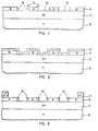
- the structure shown in FIG. 1 consists of a monocrystalline silicon substrate 10, an N + layer 12, which is arranged above the semiconductor substrate 10, and the layer 14 of the negative conductivity N-.
- the layer 12 have a high conductivity, where its associated parts are used as sub-collectors of bipolar transistors.
- the structure shown in Fig. 1 can be manufactured in various ways.
- the preferred technique is to use a P-monocrystalline silicon substrate 10, into which an N + layer is diffused to produce the layer 12 by a diffusion of a known type.
- an ion implantation of an N impurity such as e.g. B. arsenic, antimony or phosphorus to produce an N + layer 12 with a surface concentration between approximately 1 x 10 19 to 1 x 10 21 atoms / cm 3 .
- the layer 14 is then arranged over the layer 12 by epitaxial growth. This can be done by a known technique such as e.g. B.
- the N + layer 12 may have a thickness of approximately 1 to 3 ⁇ m, and the epitaxial layer 14 may have a thickness of approximately 0.5 to 10.
- the structure described could optionally be produced by various combinations of thermal diffusion, ion implantation and / or epitaxial growth, in such a way that the structure has a buried subcollector region if the production of a bipolar transistor is subsequently desired.
- Highly doped buried regions or layers are not necessary in certain semiconductor structures and can therefore be omitted. This applies to FET devices.
- Multi-buried, highly doped regions of differently doped semiconductor types can optionally be produced by a multiple epitaxial and diffusion process. These structures could be used for buried sub-collectors and buried conductors.
- the structure consisting of the substrate 10 of the N + layer 12 and the N layer 14 is produced by a photolithographic technique. This results from selective etching in order to produce narrow, flat channels 16 which have vertical side walls 18 and horizontal base surfaces 20, as shown in FIG. 1. As will be described in more detail later, the flat channels have a width of approximately 2.5 ⁇ or less, so that the channels are filled primarily by deposition on the vertical side walls, ie the channels are starting from the side walls and not filled starting from the base areas. This differs from filling a relatively wide channel, which would require thicker fill layers.
- a uniform layer 22 of a mask material is applied to the surface of the structure shown in FIG. 1. This coating is carried out by a vapor deposition process or by a plasma coating, so that the cover layer is applied in a uniform thickness to the horizontal and vertical surfaces of the etched semiconductor structure.
- the thickness of the layer 22 is equal to the width of one of the semiconductor intermediate walls arranged at intervals and described with reference to FIG. 4.
- the coated semiconductor body is exposed to a reactive ion etching in order to remove the layer 22 from the horizontal surface parts, so that the layer 22 is only retained on the vertical surface parts of the structure as shown in FIG. 3.
- a suitable steam coating method and a reactive ion etching for the removal of the layer 22 from the horizontal surfaces of the structure are described by the European patent application EP 7 910 33 51.7 (EP-A-10596). From this description it emerges that it is important that the etched semiconductor body according to the illustration according to FIG. 1 has vertical side surfaces which have an inclination to the base area of less than 5 °, so that after ion ion etching the one shown in FIG. 3 Structure is achieved.
- the uniform layer 22 may be made from a variety of materials or combinations of materials that include silicon dioxide, silicon nitride, or aluminum oxide.
- FIG. 3 The desired result of the etching process described is shown in FIG. 3, the uniform coating 22 being removed from the horizontal surfaces of the semiconductor body. There is no effect on the vertical surfaces 18 of the layer in the channels 16. The result is the narrow areas 24 of the originally uniform layer 22, as shown in FIG. 3.
- the structure shown in Fig. 3 is subjected to reactive ion etching to achieve the desired width and depth of the channels by using the remaining uniform layer parts 24 as an etching mask. 4 shows the result of this method. It should be noted that all channels extend to the region P 1 of the substrate 10.
- a P region below the dielectric material used to fill the etched channels shown in FIG. 4 is desirable when the substrate is made of a P material according to the present Example.
- the P - area has, so far that its material changes the tendency to change its resistance value to the N-type, when it is subjected to thermal oxidation.
- a P * implantation in the substrate 10 on the bases of the individual etched channels prevents the possibility of such a reversal. This can be done by using a P + ion implantation of a dopant, e.g. B. boron can be prevented. Accordingly, a thin layer of silicon dioxide is applied to the structure shown in FIG. 4, which serves as a protective screen for the boron ion implantation mentioned, and the ion implantation is carried out in order to increase the P + stop thresholds 26 shown in FIG. 5 produce.
- the structure is thermally oxidized in order to convert all of the silicon in the partition walls 28 shown in FIG. 4 into silicon dioxide.
- the thermally grown silicon dioxide of the partition walls fills the regions 30, as shown in FIG. 5.
- 30 unfilled interstices 32 remain in the regions remaining as shown in FIG. 5. These are filled by the vapor deposition or plasma deposition of silicon dioxide or by other dielectric material.
- the applied dielectric material is removed from the surfaces of the semiconductor body in a known manner corresponding to the regions 34 by selective ion etching.
Landscapes
- Element Separation (AREA)
- Local Oxidation Of Silicon (AREA)
- Drying Of Semiconductors (AREA)
Claims (2)
Applications Claiming Priority (2)
| Application Number | Priority Date | Filing Date | Title |
|---|---|---|---|
| US06/052,997 US4211582A (en) | 1979-06-28 | 1979-06-28 | Process for making large area isolation trenches utilizing a two-step selective etching technique |
| SA52997 | 1979-06-28 |
Publications (3)
| Publication Number | Publication Date |
|---|---|
| EP0021147A2 EP0021147A2 (fr) | 1981-01-07 |
| EP0021147A3 EP0021147A3 (en) | 1983-04-06 |
| EP0021147B1 true EP0021147B1 (fr) | 1986-01-29 |
Family
ID=21981249
Family Applications (1)
| Application Number | Title | Priority Date | Filing Date |
|---|---|---|---|
| EP80103086A Expired EP0021147B1 (fr) | 1979-06-28 | 1980-06-03 | Procédé pour la fabrication de fossés d'isolation larges et profonds dans un substrat semiconducteur |
Country Status (6)
| Country | Link |
|---|---|
| US (1) | US4211582A (fr) |
| EP (1) | EP0021147B1 (fr) |
| JP (1) | JPS5837987B2 (fr) |
| CA (1) | CA1139017A (fr) |
| DE (1) | DE3071381D1 (fr) |
| IT (1) | IT1149834B (fr) |
Families Citing this family (67)
| Publication number | Priority date | Publication date | Assignee | Title |
|---|---|---|---|---|
| US4274909A (en) * | 1980-03-17 | 1981-06-23 | International Business Machines Corporation | Method for forming ultra fine deep dielectric isolation |
| US4287661A (en) * | 1980-03-26 | 1981-09-08 | International Business Machines Corporation | Method for making an improved polysilicon conductor structure utilizing reactive-ion etching and thermal oxidation |
| US4378630A (en) * | 1980-05-05 | 1983-04-05 | International Business Machines Corporation | Process for fabricating a high performance PNP and NPN structure |
| US4394196A (en) * | 1980-07-16 | 1983-07-19 | Tokyo Shibaura Denki Kabushiki Kaisha | Method of etching, refilling and etching dielectric grooves for isolating micron size device regions |
| JPS5748237A (en) * | 1980-09-05 | 1982-03-19 | Nec Corp | Manufacture of 2n doubling pattern |
| JPS5758356A (en) * | 1980-09-26 | 1982-04-08 | Toshiba Corp | Manufacture of semiconductor device |
| US4400715A (en) * | 1980-11-19 | 1983-08-23 | International Business Machines Corporation | Thin film semiconductor device and method for manufacture |
| US4415371A (en) * | 1980-12-29 | 1983-11-15 | Rockwell International Corporation | Method of making sub-micron dimensioned NPN lateral transistor |
| DE3102647A1 (de) * | 1981-01-27 | 1982-08-19 | Siemens AG, 1000 Berlin und 8000 München | Strukturierung von metalloxidmasken, insbesondere durch reaktives ionenstrahlaetzen |
| JPS57170533A (en) * | 1981-04-13 | 1982-10-20 | Nec Corp | Forming method for mask pattern |
| DE3279874D1 (en) * | 1981-08-21 | 1989-09-14 | Toshiba Kk | Method of manufacturing dielectric isolation regions for a semiconductor device |
| GB2104287B (en) * | 1981-08-21 | 1985-02-20 | Gen Electric Co Plc | Data storage devices |
| US4491486A (en) * | 1981-09-17 | 1985-01-01 | Tokyo Shibaura Denki Kabushiki Kaisha | Method for manufacturing a semiconductor device |
| US4432132A (en) * | 1981-12-07 | 1984-02-21 | Bell Telephone Laboratories, Incorporated | Formation of sidewall oxide layers by reactive oxygen ion etching to define submicron features |
| US4424621A (en) | 1981-12-30 | 1984-01-10 | International Business Machines Corporation | Method to fabricate stud structure for self-aligned metallization |
| US4430791A (en) * | 1981-12-30 | 1984-02-14 | International Business Machines Corporation | Sub-micrometer channel length field effect transistor process |
| US4385975A (en) * | 1981-12-30 | 1983-05-31 | International Business Machines Corp. | Method of forming wide, deep dielectric filled isolation trenches in the surface of a silicon semiconductor substrate |
| JPS58217499A (ja) * | 1982-06-10 | 1983-12-17 | Toshiba Corp | 薄膜の微細加工方法 |
| US4444605A (en) * | 1982-08-27 | 1984-04-24 | Texas Instruments Incorporated | Planar field oxide for semiconductor devices |
| JPS59132627A (ja) * | 1983-01-20 | 1984-07-30 | Matsushita Electronics Corp | パタ−ン形成方法 |
| US4771328A (en) * | 1983-10-13 | 1988-09-13 | International Business Machine Corporation | Semiconductor device and process |
| USH204H (en) | 1984-11-29 | 1987-02-03 | At&T Bell Laboratories | Method for implanting the sidewalls of isolation trenches |
| US4648173A (en) * | 1985-05-28 | 1987-03-10 | International Business Machines Corporation | Fabrication of stud-defined integrated circuit structure |
| US4753901A (en) * | 1985-11-15 | 1988-06-28 | Ncr Corporation | Two mask technique for planarized trench oxide isolation of integrated devices |
| US4801350A (en) * | 1986-12-29 | 1989-01-31 | Motorola, Inc. | Method for obtaining submicron features from optical lithography technology |
| US5130268A (en) * | 1991-04-05 | 1992-07-14 | Sgs-Thomson Microelectronics, Inc. | Method for forming planarized shallow trench isolation in an integrated circuit and a structure formed thereby |
| US5292689A (en) * | 1992-09-04 | 1994-03-08 | International Business Machines Corporation | Method for planarizing semiconductor structure using subminimum features |
| US5290358A (en) * | 1992-09-30 | 1994-03-01 | International Business Machines Corporation | Apparatus for directional low pressure chemical vapor deposition (DLPCVD) |
| JP3324832B2 (ja) * | 1993-07-28 | 2002-09-17 | 三菱電機株式会社 | 半導体装置およびその製造方法 |
| US5372968A (en) * | 1993-09-27 | 1994-12-13 | United Microelectronics Corporation | Planarized local oxidation by trench-around technology |
| US5366925A (en) * | 1993-09-27 | 1994-11-22 | United Microelectronics Corporation | Local oxidation of silicon by using aluminum spiking technology |
| US5294562A (en) * | 1993-09-27 | 1994-03-15 | United Microelectronics Corporation | Trench isolation with global planarization using flood exposure |
| US5308786A (en) * | 1993-09-27 | 1994-05-03 | United Microelectronics Corporation | Trench isolation for both large and small areas by means of silicon nodules after metal etching |
| KR960014452B1 (ko) * | 1993-12-22 | 1996-10-15 | 금성일렉트론 주식회사 | 반도체 소자분리 방법 |
| US5395790A (en) * | 1994-05-11 | 1995-03-07 | United Microelectronics Corp. | Stress-free isolation layer |
| US5374583A (en) * | 1994-05-24 | 1994-12-20 | United Microelectronic Corporation | Technology for local oxidation of silicon |
| US5904539A (en) * | 1996-03-21 | 1999-05-18 | Advanced Micro Devices, Inc. | Semiconductor trench isolation process resulting in a silicon mesa having enhanced mechanical and electrical properties |
| US5742090A (en) * | 1996-04-04 | 1998-04-21 | Advanced Micro Devices, Inc. | Narrow width trenches for field isolation in integrated circuits |
| WO1997038442A1 (fr) * | 1996-04-10 | 1997-10-16 | Advanced Micro Devices, Inc. | Isolement de tranchee de semi-conducteur associe a une methodologie amelioree de planarisation |
| US5926713A (en) * | 1996-04-17 | 1999-07-20 | Advanced Micro Devices, Inc. | Method for achieving global planarization by forming minimum mesas in large field areas |
| US5899727A (en) * | 1996-05-02 | 1999-05-04 | Advanced Micro Devices, Inc. | Method of making a semiconductor isolation region bounded by a trench and covered with an oxide to improve planarization |
| US6306727B1 (en) * | 1997-08-18 | 2001-10-23 | Micron Technology, Inc. | Advanced isolation process for large memory arrays |
| WO2000003560A2 (fr) | 1998-07-08 | 2000-01-20 | Infineon Technologies Ag | Procede permettant de former une depression remplie dans une couche de materiau, et circuit integre fabrique selon ledit procede |
| US6207534B1 (en) * | 1999-09-03 | 2001-03-27 | Chartered Semiconductor Manufacturing Ltd. | Method to form narrow and wide shallow trench isolations with different trench depths to eliminate isolation oxide dishing |
| US6218244B1 (en) * | 1999-12-10 | 2001-04-17 | Taiwan Semiconductor Mfg Co Ltd | Method of fabricating transistor |
| DE10041084A1 (de) | 2000-08-22 | 2002-03-14 | Infineon Technologies Ag | Verfahren zur Bildung eines dielektrischen Gebiets in einem Halbleitersubstrat |
| US6962831B2 (en) * | 2002-01-16 | 2005-11-08 | The Regents Of The University Of Michigan | Method of making a thick microstructural oxide layer |
| DE10345990B4 (de) * | 2003-10-02 | 2008-08-14 | Infineon Technologies Ag | Verfahren zum Erzeugen einer Oxidschicht |
| US7023069B2 (en) * | 2003-12-19 | 2006-04-04 | Third Dimension (3D) Semiconductor, Inc. | Method for forming thick dielectric regions using etched trenches |
| TWI401749B (zh) * | 2004-12-27 | 2013-07-11 | 3D半導體股份有限公司 | 用於高電壓超接面終止之方法 |
| US7439583B2 (en) * | 2004-12-27 | 2008-10-21 | Third Dimension (3D) Semiconductor, Inc. | Tungsten plug drain extension |
| JP2008538659A (ja) * | 2005-04-22 | 2008-10-30 | アイスモス テクノロジー コーポレイション | 酸化物で内面が覆われた溝を有する超接合素子と酸化物で内面を覆われた溝を有する超接合素子を製造するための方法 |
| US7446018B2 (en) | 2005-08-22 | 2008-11-04 | Icemos Technology Corporation | Bonded-wafer superjunction semiconductor device |
| US7955961B2 (en) * | 2006-03-07 | 2011-06-07 | International Rectifier Corporation | Process for manufacture of trench Schottky |
| US7429772B2 (en) * | 2006-04-27 | 2008-09-30 | Icemos Technology Corporation | Technique for stable processing of thin/fragile substrates |
| US8580651B2 (en) * | 2007-04-23 | 2013-11-12 | Icemos Technology Ltd. | Methods for manufacturing a trench type semiconductor device having a thermally sensitive refill material |
| US7723172B2 (en) * | 2007-04-23 | 2010-05-25 | Icemos Technology Ltd. | Methods for manufacturing a trench type semiconductor device having a thermally sensitive refill material |
| US20080272429A1 (en) * | 2007-05-04 | 2008-11-06 | Icemos Technology Corporation | Superjunction devices having narrow surface layout of terminal structures and methods of manufacturing the devices |
| US20090085148A1 (en) * | 2007-09-28 | 2009-04-02 | Icemos Technology Corporation | Multi-directional trenching of a plurality of dies in manufacturing superjunction devices |
| US7846821B2 (en) * | 2008-02-13 | 2010-12-07 | Icemos Technology Ltd. | Multi-angle rotation for ion implantation of trenches in superjunction devices |
| US8030133B2 (en) * | 2008-03-28 | 2011-10-04 | Icemos Technology Ltd. | Method of fabricating a bonded wafer substrate for use in MEMS structures |
| US8815700B2 (en) * | 2008-12-08 | 2014-08-26 | Texas Instruments Incorporated | Method of forming high lateral voltage isolation structure involving two separate trench fills |
| US9111994B2 (en) * | 2010-11-01 | 2015-08-18 | Magnachip Semiconductor, Ltd. | Semiconductor device and method of fabricating the same |
| US8946814B2 (en) | 2012-04-05 | 2015-02-03 | Icemos Technology Ltd. | Superjunction devices having narrow surface layout of terminal structures, buried contact regions and trench gates |
| US9576842B2 (en) | 2012-12-10 | 2017-02-21 | Icemos Technology, Ltd. | Grass removal in patterned cavity etching |
| US8652934B1 (en) | 2012-12-26 | 2014-02-18 | Micron Technology, Inc. | Semiconductor substrate for photonic and electronic structures and method of manufacture |
| US9006080B2 (en) * | 2013-03-12 | 2015-04-14 | Taiwan Semiconductor Manufacturing Company, Ltd. | Varied STI liners for isolation structures in image sensing devices |
Family Cites Families (10)
| Publication number | Priority date | Publication date | Assignee | Title |
|---|---|---|---|---|
| US3938241A (en) * | 1972-10-24 | 1976-02-17 | Motorola, Inc. | Vertical channel junction field-effect transistors and method of manufacture |
| US3966577A (en) * | 1973-08-27 | 1976-06-29 | Trw Inc. | Dielectrically isolated semiconductor devices |
| JPS5131186A (fr) * | 1974-09-11 | 1976-03-17 | Hitachi Ltd | |
| JPS5146083A (en) * | 1974-10-18 | 1976-04-20 | Hitachi Ltd | Handotaisochino seizohoho |
| GB1485015A (en) * | 1974-10-29 | 1977-09-08 | Mullard Ltd | Semi-conductor device manufacture |
| GB1527894A (en) * | 1975-10-15 | 1978-10-11 | Mullard Ltd | Methods of manufacturing electronic devices |
| US4044452A (en) * | 1976-10-06 | 1977-08-30 | International Business Machines Corporation | Process for making field effect and bipolar transistors on the same semiconductor chip |
| US4104086A (en) * | 1977-08-15 | 1978-08-01 | International Business Machines Corporation | Method for forming isolated regions of silicon utilizing reactive ion etching |
| US4139442A (en) * | 1977-09-13 | 1979-02-13 | International Business Machines Corporation | Reactive ion etching method for producing deep dielectric isolation in silicon |
| US4140558A (en) * | 1978-03-02 | 1979-02-20 | Bell Telephone Laboratories, Incorporated | Isolation of integrated circuits utilizing selective etching and diffusion |
-
1979
- 1979-06-28 US US06/052,997 patent/US4211582A/en not_active Expired - Lifetime
-
1980
- 1980-03-18 JP JP55033494A patent/JPS5837987B2/ja not_active Expired
- 1980-04-14 CA CA000349765A patent/CA1139017A/fr not_active Expired
- 1980-05-13 IT IT21996/80A patent/IT1149834B/it active
- 1980-06-03 DE DE8080103086T patent/DE3071381D1/de not_active Expired
- 1980-06-03 EP EP80103086A patent/EP0021147B1/fr not_active Expired
Also Published As
| Publication number | Publication date |
|---|---|
| IT1149834B (it) | 1986-12-10 |
| US4211582A (en) | 1980-07-08 |
| JPS566450A (en) | 1981-01-23 |
| EP0021147A2 (fr) | 1981-01-07 |
| CA1139017A (fr) | 1983-01-04 |
| EP0021147A3 (en) | 1983-04-06 |
| DE3071381D1 (en) | 1986-03-13 |
| JPS5837987B2 (ja) | 1983-08-19 |
| IT8021996A0 (it) | 1980-05-13 |
Similar Documents
| Publication | Publication Date | Title |
|---|---|---|
| EP0021147B1 (fr) | Procédé pour la fabrication de fossés d'isolation larges et profonds dans un substrat semiconducteur | |
| DE10362334B4 (de) | Halbleitervorrichtung mit epitaktisch gefülltem Graben und Verfahren zur Herstellung einer Halbleitervorrichtung mit epitaktisch gefülltem Graben | |
| DE102005046711B4 (de) | Verfahren zur Herstellung eines vertikalen MOS-Halbleiterbauelementes mit dünner Dielektrikumsschicht und tiefreichenden vertikalen Abschnitten | |
| EP0001574B1 (fr) | Dispositif semiconducteur pour structures de résistance dans des circuits intégrés de haute densité et procédé pour sa fabrication | |
| DE3129558C2 (fr) | ||
| DE102017113864B4 (de) | Verfahren zum Herstellen einer Justiermarke | |
| EP0001100A2 (fr) | Procédé de formation de régions diélectriques d'isolation encastrées dans le silicium au moyen de particules chargées et accélérées | |
| DE2502235A1 (de) | Ladungskopplungs-halbleiteranordnung | |
| DE102017115412A1 (de) | Verfahren zur Herstellung eines Supberjunctionbauelements | |
| DE60032660T2 (de) | Verfahren zur Herstellung einer planaren Heterostruktur | |
| DE2238450A1 (de) | Halbleiterbaugruppe und verfahren zur herstellung derselben | |
| DE10341755A1 (de) | Halbleitervorrichtung | |
| DE2328090A1 (de) | Halbleiterkondensator mit grosser kapazitaet und verfahren zu seiner herstellung | |
| DE2510593C3 (de) | Integrierte Halbleiter-Schaltungsanordnung | |
| DE102018105741B3 (de) | Verfahren zum erzeugen komplementär dotierter halbleitergebiete in einem halbleiterkörper und halbleiteranordnung | |
| DE102018106124B3 (de) | Verfahren zum Erzeugen eines Superjunction-Transistorbauelements | |
| DE1965406A1 (de) | Monolithische integrierte Schaltungen und Verfahren zu ihrer Herstellung | |
| DE2133976B2 (de) | Monolithisch integrierte Halbleiteranordnung | |
| DE3625742C2 (de) | Integrierte CMOS-Schaltung | |
| DE102018130444B4 (de) | Verfahren zum Herstellen eines Superjunction-Transistorbauelements | |
| DE102017118957A1 (de) | Herstellen eines superjunction-transistorbauelements | |
| DE3842749A1 (de) | Verfahren zum herstellen einer integrierten schaltung | |
| DE2904480B2 (de) | Integrierte Halbleiterschaltung und Verfahren zu ihrem Herstellen | |
| DE1965408C3 (de) | Verfahren zum Herstellen eines Halbleiterbauelementes | |
| DE102018132435A1 (de) | Verfahren zum Herstellen eines Superjunction-Transistorbauelements |
Legal Events
| Date | Code | Title | Description |
|---|---|---|---|
| PUAI | Public reference made under article 153(3) epc to a published international application that has entered the european phase |
Free format text: ORIGINAL CODE: 0009012 |
|
| AK | Designated contracting states |
Designated state(s): DE FR GB |
|
| 19U | Interruption of proceedings before grant |
Effective date: 19801017 |
|
| 19U | Interruption of proceedings before grant |
Effective date: 19801017 |
|
| 19W | Proceedings resumed before grant after interruption of proceedings |
Effective date: 19810223 |
|
| 17P | Request for examination filed |
Effective date: 19810909 |
|
| PUAL | Search report despatched |
Free format text: ORIGINAL CODE: 0009013 |
|
| AK | Designated contracting states |
Designated state(s): DE FR GB |
|
| GRAA | (expected) grant |
Free format text: ORIGINAL CODE: 0009210 |
|
| AK | Designated contracting states |
Kind code of ref document: B1 Designated state(s): DE FR GB |
|
| REF | Corresponds to: |
Ref document number: 3071381 Country of ref document: DE Date of ref document: 19860313 |
|
| ET | Fr: translation filed | ||
| PLBE | No opposition filed within time limit |
Free format text: ORIGINAL CODE: 0009261 |
|
| STAA | Information on the status of an ep patent application or granted ep patent |
Free format text: STATUS: NO OPPOSITION FILED WITHIN TIME LIMIT |
|
| 26N | No opposition filed | ||
| PGFP | Annual fee paid to national office [announced via postgrant information from national office to epo] |
Ref country code: FR Payment date: 19900529 Year of fee payment: 11 |
|
| PGFP | Annual fee paid to national office [announced via postgrant information from national office to epo] |
Ref country code: DE Payment date: 19900707 Year of fee payment: 11 |
|
| PGFP | Annual fee paid to national office [announced via postgrant information from national office to epo] |
Ref country code: GB Payment date: 19910523 Year of fee payment: 12 |
|
| PG25 | Lapsed in a contracting state [announced via postgrant information from national office to epo] |
Ref country code: FR Effective date: 19920228 |
|
| PG25 | Lapsed in a contracting state [announced via postgrant information from national office to epo] |
Ref country code: DE Effective date: 19920401 |
|
| REG | Reference to a national code |
Ref country code: FR Ref legal event code: ST |
|
| PG25 | Lapsed in a contracting state [announced via postgrant information from national office to epo] |
Ref country code: GB Effective date: 19920603 |
|
| GBPC | Gb: european patent ceased through non-payment of renewal fee |
Effective date: 19920603 |