EP0022814B1 - Speichersystem für ein datenverarbeitungssystem - Google Patents
Speichersystem für ein datenverarbeitungssystem Download PDFInfo
- Publication number
- EP0022814B1 EP0022814B1 EP80900180A EP80900180A EP0022814B1 EP 0022814 B1 EP0022814 B1 EP 0022814B1 EP 80900180 A EP80900180 A EP 80900180A EP 80900180 A EP80900180 A EP 80900180A EP 0022814 B1 EP0022814 B1 EP 0022814B1
- Authority
- EP
- European Patent Office
- Prior art keywords
- memory
- signal
- data
- buffer
- page
- Prior art date
- Legal status (The legal status is an assumption and is not a legal conclusion. Google has not performed a legal analysis and makes no representation as to the accuracy of the status listed.)
- Expired
Links
Images



Classifications
-
- G—PHYSICS
- G06—COMPUTING OR CALCULATING; COUNTING
- G06F—ELECTRIC DIGITAL DATA PROCESSING
- G06F12/00—Accessing, addressing or allocating within memory systems or architectures
- G06F12/02—Addressing or allocation; Relocation
- G06F12/08—Addressing or allocation; Relocation in hierarchically structured memory systems, e.g. virtual memory systems
- G06F12/0802—Addressing of a memory level in which the access to the desired data or data block requires associative addressing means, e.g. caches
- G06F12/0864—Addressing of a memory level in which the access to the desired data or data block requires associative addressing means, e.g. caches using pseudo-associative means, e.g. set-associative or hashing
Definitions
- the present invention relates to a memory system for use in a data processing system in which processing means is arranged to provide over a memory bus a memory request instruction which includes the address of the memory location to be accessed.
- the invention has application, for example, to a memory system of the kind specified above having a main memory comprising charge-coupled devices (CCD).
- CCD charge-coupled devices
- MOS metal oxide semiconductor
- RAM dynamic random-access memories
- Present CCD memory technology has fabricated CCD memories having four times the density per package at one quarter the cost per bit of dynamic RAM memory.
- one disadvantage of CCD memories systems is their slower access time as compared to random-access memories employing MOS technology.
- a memory system including a main memory having a relatively slow speed of access in which processing means is arranged to provide over a memory bus a memory request instruction which includes the address in the main memory of the memory location to be accessed.
- the system includes a plurality of independently accessible buffer memories coupled to said main memory for storing a portion of the data stored in said main memory, said buffer memories each having a relatively fast speed of access compared with said main memory and said bus being common to said main memory and said buffer memories, an address register for each of said buffer memories for storing an address designating the memory location of the data stored in the associated buffer memory, address comparison means coupled to said bus and each address register for providing an active output signal when said comparison means determines that an addressed memory location is located in a buffer memory, and circuit means coupled to said comparison means and responsive to said active output signal to provide a signal enabling the buffer memory containing the memory location to be accessed by the processing means.
- a problem experienced with memory systems of the kind disclosed in the previously mentioned article in IBM Technical Disclosure Bulletin is that the address of a data word in the main memory is shifted when transferred into a buffer memory due to the difference in speed between the two memories.
- a memory system including a main memory for use in a data processing system in which processing means is arranged to provide over a memory bus a memory request instruction which includes the address in said main memory of the memory location to be accessed, and further including first and second independently accessible buffer memories coupled to said main memory for storing a portion of the data stored in said main memory, said buffer memories each having a relatively fast speed of access compared with said main memory and said bus being common to said main memory and said buffer memories, an address register for each of said buffer memories for storing an address designating the memory location of the data stored in the associated buffer memory, address comparison means coupled to said bus and each address register for providing an active output signal when said comparison means determines that an addressed memory location is located in a buffer memory, and circuit means coupled to said comparison means and responsive to said active output signal to provide an enabling signal enabling the buffer memory containing the memory location to be accessed by the processing means, characterized in that said circuit means is arranged to generate a first control signal to effect the transfer of data from said main memory to
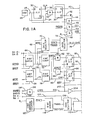
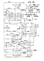
- FIG. 1A and 1B there is disclosed a block diagram of a memory system of a data processing system having a central processing unit (CPU) in which data for the system is stored in a CCD memory device 20 (Fig. 1 B) having a capacity of 65Kx 16 bit words of data.
- a CCD memory device 20 (Fig. 1 B) having a capacity of 65Kx 16 bit words of data.
- An example of such memory device which is presently commercially available is Texas Instruments TMS 3064 based on a 16 bit word size.
- the CCD memory device 20 has stored therein 16 blocks or pages of data with each page comprising 4,096x16 bit words of data.
- Each page address of a 16 bit memory access data request generated by the CPU is a 4 bit field with 12 bits reserved for addressing data within a particular page.
- a pair of buffer memories 22 and 24 (Fig. 1B) each comprised of sixteen 4,096x 1 static RAM memory devices which provides a relatively highspeed memory access.
- An example of a commercially-available static RAM memory device that may be utilized in the present embodiment is Texas Instruments TMS 4044.
- the RAM buffers 22 and 24 each contains a page or block of data transferred from the CCD memory 20, the buffer memories together with the CCD memory 20 being interfaced with the CPU (not shown) over a common bus in a manner that is well-known in the art.
- the CPU executes program instructions out of the two RAM buffers 22 and 24 in a manner that is well-known in the art.
- the CCD memory 20 remains transparent to the CPU and, similarly, the CPU remains transparent to the CCD memory 20.
- the 4 bit page address field of the access request is compared with the address of the pages stored in the buffers 22 and 24. If a comparison is found, data may be read from or written into the appropriate page buffer in which the requested address has been found. If no comparison is found, the CPU is forced into a wait state until a new block or page of data is transferred from the CCD memory 20 to the buffer memory not responsible for issuing the memory access request allowing a memory access to occur at a high execution rate as will be explained more fully hereinafter.
- the memory system of the present embodiment includes a clock circuit for generating timing clock signals ⁇ , and (P2 used in accessing the data in the CCD memory 20.
- a clock circuit for generating timing clock signals ⁇ , and (P2 used in accessing the data in the CCD memory 20.
- positive logic is used throughout the logic circuits to be described hereinafter. Certain of the logical elements found therein will be identified by their part numbers, which are manufactured by a number of companies, for example, Texas Instruments Inc. The signals are illustrated in the drawings in their active state.
- a 20 Mhz. oscillator 26 whose output clock signals over line 28 toggles a LS74 D-type flip-flop 30.
- the output clock pulse of oscillator 26 is also coupled to one input of a NAND gate 32 over line 34.
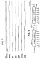
- the 20 Mhz. clock signal is shown in Fig. 6.
- the Q output of the flip-flop 30 provides a 10 Mhz. clock pulse width which is designated CLK (Fig. 6) on line 38 and is also coupled to the other input of the NAND gate 32 whose output pulse will toggle a second LS74 D-type flip-flop 36 producing the ⁇ 2 clock pulse which in the present instance has a pulse width of 100 ns.
- the output clock pulse of NAND gate 32 and the ⁇ 2 clock pulse are shown in Fig. 6.
- the ⁇ 2 clock is produced on the Q output line 40 of the flip-flop 36 while a 2 clock pulse appears on the output line 42.
- the 2 clock pulse is coupled to the D input of the flip-flop 36 enabling the flip-flop 36 to output the clock pulse ⁇ 2 and T 2 .
- the '0 2 clock pulse is also coupled to one of the inputs of the NAND gates 44 and 46 (Fig. 1A).
- the other input of the NAND gate 44 receives the 7i output of the flip-flop 30 to output a ⁇ 1 clock pulse over line 48 having a pulse width of 50 ns. as shown in Fig. 6.
- the ⁇ 1 clock pulse is coupled to an inverter 50 (Fig. 1 B) to produce the 1 clock pulse over line 52 for use in accessing the CCD memory 20 as will be described hereinafter.
- the ⁇ 1 clock pulse is also coupled to one input of an AND gate 54 (Fig. 1A) whose output pulse is the CCD memory 20 chip select signal CCS used in accessing the CCD memory 20 in a manner that is well-known in the art.
- the other input of the AND gate 54 receives a control signal designated as TRANS which becomes high when the transfer of data word between the RAM buffers 22 and 24 and the CCD memory 20 reaches a predetermined number, in this case either 4,100 or 8,196.
- TRANS becomes high
- the control signal CCS disables the transfer operation of the CCD memory as will be explained more fully herein--after.
- the control signal TRANS which is generated in the control circuit 90 (Fig. 1 B) is also coupled to an input of the NAND gate 46 whose other input receives the 2 clock pulse from the Q output of flip-flop 36 thereby enabling the NAND gate 46 to output over line 56 the chip enable control signal designated as CCE for use in accessing the CCD memory 20 in a manner that is well-known in the art.
- the CCE signal is coupled to an appropriate CCE driver 58 (Fig. 1B) for use in accessing the CCD memory 20.
- Also included in the accessing of the CCD memory 20 are the ⁇ 1 driver 60 and the ⁇ 2 driver 62 which also function in a manner that is well known in the art.
- a 16 bit address is transmitted over a common bus which includes lines 64 (Fig. 1A), in which address bits BA12-BA15 are found comprising the address of the page in which the requested address identifying the data to be accessed is located.
- the data bits BA12-BA15 are coupled to the inputs of two four-bit address latches 66 and 68 each associated with one of the buffers 22 and 24.
- the latches 66 and 68 may be SNLS175 flip-flops available from Texas Instruments, Inc.
- the latch 66 associated with the buffer 22 stores the address of the page of data contained in the CCD memory that is now stored in the buffer 22.
- Latch 68 functions in the same manner with respect to buffer 24.
- each of the latches 66 and 68 is coupled over line 69 to the input of a 2-1 data selector 70 whose output is coupled to one input of a second data selector 72 whose other input receives the page address bits BA12-BA15 over lines 64.
- the data selectors 70 and 72 multiplex the address of the page that is to be transferred from the CCD memory 20 (Fig. 1 B) to the buffers 22 and 24.
- the data selector 72 transmits the address of a page identified as bits CA12-CA15 in Fig. 1A which may comprise one of the page addresses stored in the 4 bit latches 66 and 68 or the page address identified by the data bits BA12-BA15 appearing on the common bus lines 64.
- the page address bits CA12-CA15 are coupled to the CCD memory 20 over line 74.
- the data selectors 70 and 72 may be SN54LS157 multiplexers available from Texas Instruments, Inc.
- the outputs of the 4 bit latches 66 and 68 are each coupled over line 75 to one input of an associated 4 bit comparator 76 and 78 respectively.
- the other inputs of the comparators 76 and 78 are coupled to the common bus lines 64 to receive the requested page address bits BA12-BA15 currently appearing on the lines 64.
- the comparators 76 and 78 will compare the requested page address with the page addresses currently stored in the RAM buffers 22 and 24 (Fig. 1 B) as represented by the output of the 4 bit latches 66 and 68 to determine if a further search of the CCD memory 20 is required.
- the system will access the page of data stored in the appropriate buffer in an access time associated with RAM memories. If no comparison is found, the system will force the CPU into a wait mode while the page containing the address requested by the CPU is transferred from the CCD memory to one of the buffers 22 and 24 in a manner that will now be described.
- CMPO or CMP1 appearing on the output lines 80 and 88 of the comparators 76 and 78 respectively will go high in accordance with the comparison found therein.
- the signal CMPO is outputted over line 80 to one input of a NAND gate 82 and also to the inverter 98 whose output is coupled to the J input of a SN54LS109 J-K flip-flop 96.
- the output signal CMP1 of the 4 bit comparators 78 is coupled to the other input of the NAND gate 82 over line 88 and also to the Kinput of the flip-flop 96.
- the Q output of the flip-flop 96 is coupled over line 97 to one input of a non-inverting NAND gate 100 (Fig. 1B) while the output of the flip-flop 96 is coupled to a second non-inverting NAND gate 102 (Fig. 1 B).
- the NAND gates 100 and 102 are enabled by a signal receive over line 107 from the output of an inverter 108 (Fig. 1B) to output the page pointer signals MCSO and MCS1 which are the chip enable signals for the RAM buffers 22 and 24 (Fig. 1 B) and which when active low point to the RAM buffer in which a comparison was found. It will be appreciated that in generating the chip enable signal MCS0 and MCS1 the RAM buffer in which the requested page of data is stored is automatically enabled to be accessed by the system.
- the flip-flop 96 will be toggled by the level of the compare signals CMPO and CMP1 to output the corresponding active low control signal MCS0 or MCS1 thereby enabling its associated RAM buffer 22 or 24 to accept the address bits BAO-BA11 appearing on the common bus lines 104 (Fig. 1A) and which are transmitted to a data selector 106 (Fig. 1A) for access to the appropriate buffers 22 and 24 over line 110.
- the data so accessed by the address bits BAO-BA11 are transmitted from the appropriate RAM buffer 22 or 24 over line 112 (Fig. 1B) to a data driver 114 (Fig. 1B) for transmission over a common bus line 115 to the CPU.
- the flip-flop 96 will automatically be toggled to output one of the signals MCS0 or MCS 1 indicating the buffer having the oldest used data contained therein.
- the data selector 106 which may be of the same construction as data selectors 70 and 72 (Fig. 1A) is enabled by the level of the signal TRANS to select either the data bits BA0BA11 appearing on the common bus lines 104 (Fig. 1A) for accessing into the RAM buffers 22 or 24 or the output of a SN54LS161 12 bit adder 118 (Fig. 1A) which outputs data bits CAO-CA11 comprising a data address based on the output count of a SN54LS83 12 bit address counter 120.
- the address bits CAO-CA11 are used in transferring data between the CCD memory 20 and the RAM buffers 22 and 24 and may reflect the difference in speed between the slower CCD memory 20 and the faster RAM buffer memories 22 and 24 in locating the same bit location in both types of memory structures.
- the comparators 76 and 78 do not find a comparison, the output signals CMPO and CMP1 (Fig. 1A) will be low enabling the NAND gate 82 (Fig. 1A) to output a binary one to the J input of a SN54LS109A J- K flip-flop 92 resulting in the appearance on its Q output line 93 of the active high non-compare signal NOCMP together with the appearance on the 7T output of the active low bus ready signal BRDY upon the clocking of the flip-flop 92.
- the active low signal BRDY is transmitted over the bus line 95 to the CPU which puts the CPU into a wait mode until the requested page is transferred from the CCD memory 20 to either of the buffers 22 and 24.
- a clock signal CREQ for clocking the flip-flops 92 and 96 (Figs. 1A and 8) is generated based on the bus memory request signal BMREQ (Fig. 7) transmitted from the CPU becoming active.
- the active high output signal NOCMP (Fig. 1B) is transmitted to the control circuit 90 (Fig. 1B) which, as will be described more fully hereinafter, will generate the control signals TRANS and TRANS which effect a transfer operation.
- the signal NOCMP will be high when a comparison is not found between the page address data bits BA12-BA15 appearing on the bus line 64 with the page address data stored in the 4 bit latches 66 and 68 representing the address of the pages stored in the buffer memories 22 and 24.
- the signal TRANS Upon the signal NOCMP going high, the signal TRANS will go high while the signal TRANS will go low initiating a transfer operation.
- the system Since the address of the requesting page appears on the bus lines 64, the system will access the CCD memory 20 with the requesting page address and transfer the page out of the CCD memory 20 and into one of the buffer memories 22 and 24 allowing a high speed memory access to occur once the new page of data is stored in the RAM buffer memories 22 and 24.
- the address of the data word found in the CCD memory is shifted when transferred into the buffer memories 22 and 24 due to the difference in speed between the two memories.
- a memory location in the CCD memory 20 when transferred into the RAM buffer memory will not be at the same location in the latter memory due to the faster speed of the buffer memory.
- the 12 bit address counter 120 (Fig. 1A) clocked by the clock signal ⁇ 1 , will initiate a 12 bit count from 0 to 4,096 which may be used as the address of a 16 bit data word located in the buffers 22 and 24 (Fig.
- the output count of the address counter 120 is coupled to the 12 bit adder 118 (Fig. 1A) which when enabled adds 2 to every output count of the counter 120 thereby outputting the count bits CAO-CA11 comprising the data word address for each location in the RAM buffer 22 and 24.
- the adder 18 When transferring data from the CCD memory 20 to the RAM buffers 22 and 24, the adder 18 will be disabled and the address bits CAO-CA11 will correspond to the output count of the counter 120.
- a SN54LS374 16 bit latch 119 (Fig. 1B) will be enabled to output a page of data from the CCD memory 20 corresponding to the page address bits BA12-BA15 appearing on the system bus line 64 (Fig. 1A) and which were transmitted through the data selector 72 to the CCD memory 20 (Fig. 1 B).
- the page of data transmitted from the CCD memory 20 and through the 16 bit latch 119 (Fig. 1B)
- a write operation had occurred on the pages of data stored in the buffer memories 22 and 24 (Fig. 1B)
- the page is required to be transferred back into the CCD memory 20 before a new page can be read out and stored in that buffer memory. Otherwise the new page transferred from the CCD memory 20 is written over the page of data stored in the designated RAM buffer.
- a control signal CCHLD generated in the control circuits 90 (Fig. 1B) will become active low, thereby notifying the system that the page of data stored in the particular buffer being addressed has to be transmitted back to the CCD memory 20 before a new page of data can be transferred to the designated buffer.
- the control signal CCHLD going low will disable the data selector 72 (Fig.
- the page of data in which a write operation has occurred is transferred out of the buffer memories 22 and 24 into the CCD memory after which the new page of data identified by the address bits BA12-15 present on the common bus line 64 is transferred from the CCD memory 20 into one of the buffers 22 or 24.
- a counter located in the control circuits 90 counts the number of transfers between the CCD memory and the RAM buffers 22 and 24.
- the signal TRANS will go low and signal TRANS will go high enabling a new access operation to occur between the requested data addresses as represented by the data bits BAO-BA11 which are now transmitted over the bus line 104 (Fig.
- Fig. 2 there is shown a logic diagram of a pair of SN54LS393 binary counters 122 and 124 which are located in the control circuit block 90 (Fig. 1B) and which are continuously clocked by the ⁇ 1 clock to output on a plurality of output lines 126 a count between 0 and 32,768 in a manner that is well-known in the art.
- the binary counter 122 and 124 whose operation is initiated by the transfer signal TRANS going low at the start of a transfer operation will count the number of transfer operations that occur between the CCD memory 20 (Fig. 1 B) and the buffer memories 22 and 24.
- This operation requires 8,192 transfers which count is indicated when the signal appearing on line CH 13 of counter 124 goes high which signal is used to control the ending of the transfer operation.
- Other control signals include the signal appearing on line CH 11 which goes high upon the count reaching 2,048, and which is used to control portions of a transfer operation as will be described more fully hereinafter.
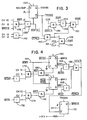
- FIG. 3 there is shown a schematic diagram of one of the logic circuits 90 (Fig. 1B) used to initiate a transfer operation together with generating signals for controlling a write operation.
- a transfer flip-flop 134 which comprises a D-type SN54LS574 flip-flop clocked by the Q1 clock and whose D-input receives the active high control signal NOCMP (Fig. 6) appearing on the Q output of the J -Kflip-flop 92 (Fig. 1A) as a result of the finding of a no comparison between the page address appearing on the common bus line 64 and the page addresses stored in the latches 66 and 68 (Fig. 1A).
- NOCMP active high control signal
- NOR gate 138 compensates for the difference in speed between the two memories and will appear on the input of the AND gate 136 whose other input contains a write disable control signal WRDIS which is high at this time enabling the NAND gate 136 to output a low signal to one of the inputs of a non-inverting NOR gate 138.
- the other inputs of the NOR gate 138 include a system reset signalRST which is high at this time and the output of a NAND gate 140 whose inputs are connected to the output lines CH2 and CH13 of counter 122 and 124 and on which appear high signals when the output of the counters 122 and 124 is at 8,196 (Fig. 6).
- both signals are low, thereby producing on the output of the NAND gate 140 a high signal which enables the NOR gate 138 to output a low signal BUFULL designating that the buffers are full.
- the signal BUFULL going low resets the transfer flip-flop 134 thereby pulling the output signal TRANS low and raising the output signal TRANS enabling the transfer operation to be terminated.
- the signal WRDIS (Fig. 6) is low during the transfer involving a write operation which disables the AND gate 136 from resetting the transfer flip-flop 134 at the count of 4100 and enabling the NOR gate 140 to output a low signal when the output lines CH2 and CH13 of the counters 122 and 124 reflect the count 8,196 as described above.
- Fig. 3 Also included in the logic circuitry shown in Fig. 3 are the generation of the buffer memory write enable signal MWE together with the CCD write enable signal CWR which enable write operations to occur in the RAM buffers 22 and 24 and the CCD memory 20 respectively.
- the control signal TRANS- will be low during the transfer operation. This signal will be transmitted into one of the inputs of the NAND gate 142 whose other input is connected to the control signal CCHLD which is high (Fig. 6) when no write operation has occurred in the RAM buffer memories 22 or 24.
- the output of the NAND gate 142 will be low which signal is transmitted to one of the inputs of the NAND gate 144 whose other input is connected to the CCD memory chip enable signal CCE (Fig. 6) generated over line 56 (Fig. 1A) from the NAND gate 46 (Fig. 1A) and the clock pulses CLK (Fig. 6) appearing over line 38 from the Q output of the flip-flop 30 in the clock circuit shown in Fig. 1A.
- CCE CCD memory chip enable signal
- CLK Fig. 6
- the output signal CWR appearing as a clock pulse will be outputted from the NAND gate 144 to the CCD memory 20 over line 148 (Fig. 1B) enabling new data to be transmitted into the CCD memory 20 through the data receiver 116 (Fig. 1B) and a 16 bit latch 220.
- the control signal CCHLD will be high, which signal is transmitted into one of the inputs of the NAND gate 142 (Fig. 3), whose other input is connected to the output of flip-flop 134 on which appears the control signal TRANS which at this time is high.
- These signals enable the output signal of the NAND gate 142 to be low which signal is coupled to one of the inputs of the non-inverting NAND gate 150 (Fig. 3).
- the other input of the NAND gate 150 is coupled to the output of a non-inverting NOR gate 152 having one input connected to the bus line 154 (Fig.
- the other input to the NOR gate 152 is coupled to the output of a NAND gate 156 which is controlled by the chip enable signal CCE and the control signal CCHLD.
- the output signal of the NAND gate 156 will go low enabling, upon the bus write signal BWR becoming active low, the output signal of the NOR gate 154 to go low.
- This signal coupled with the low signal appearing on the other input of the non-inverting NAND gate 150 will output the signal MWE in a low or active state whenever the signal CCE is high. As shown in Fig.
- the signal MWE is transmitted to each of the buffer memories 22 and 24 which coupled with the appropriate chip select signals MCS0 and MCS1 will enable one of the buffers to be accessed by the address bits which are being outputted from the data selector 106 (Fig. 1A) as described previously.
- Fig. 4 there is shown the control circuit for generating a write flag for each RAM buffer 22 and 24 (Fig. 1 B) which flag notifies the system that a write operation has occurred on the data contained in its associated RAM buffers 22 and 24.
- the write flag signals the system that in transferring a new page of data from the CCD memory 20 into the selected buffer upon the finding of a no comparison, the page of data in the selected buffer has to be transferred back to the CCD memory before a new page of data can be stored in the buffer.
- the bus write control signal BWR will be low which signal is transmitted over the common bus line 154 into the clock input of a pair of SN54LS109A J-K flip-flops 160 and 162.
- the K input of the flip-flop 160 is connected to the output of the NAND gate 100 (Fig 1B) and on which will appear the chip select signal MCS0 the buffer 22.
- the Kinput of the flip-flop 162 is similarly connected to the NAND gate 102 (Fig. 1B) whose output signal MCS1 is transmitted to the flip-flop 162.
- the chip select signal MCS0 or MCS1 associated with that buffer will be in a low state as a result of a compare operation in the manner described previously.
- the signal MCS0 would be active low (Fig. 8) resulting in the Q output signal WRFO of the flip-flop 160 going high upon the toggling of the flip-flop 160 by the control signal BWR going low (Fig. 8).
- the Q output signal WRFO of the flip-flop 160 will go low at this time which signal comprises the write flag for buffer 22 and is coupled to one input of the OR gate 164 on whose other input will appear the active low control signal MCS0 .
- the output of the OR gate 164 will go low which is coupled to one input of an AND gate 166 whose other input is connected to an OR gate 168 similarly arranged as OR gate 164 and whose output signal will be high at this time since the input signal MCS1 to the flip-flop 162 is high.
- the AND gate 166 at this time will output the active low CCD memory hold signal CCHLD which is used in controlling the transfer of a page of data on which a write operation has occurred to the CCD memory 20 (Fig. 1 B).
- the output signal CCHLD of the AND gate 166 (Fig. 4) will go low until the bus memory request signal BMREQ goes high which, as will be described more fully hereinafter, resets the flip-flop 96 (Fig. 11) in which MCSO goes high (Fig. 8).
- the output signal CCHLD goes low.
- the flip-flop 160 remains in its set condition enabling the write flag WRFO appearing on the Q output of the flip-flop 160 to condition the OR gate 164 to output a low signal upon the input signal MCSO going low when the next compare generation occurs in which the requested page is located in RAM buffer 22.
- the CCHLD signal goes low signalling the system that the page of data in buffer 22 has to be transferred to the CCD before a new page of data can be transferred from the CCD memory 20 to the RAM buffer 22.
- the RAM buffer 22 has been selected as the buffer containing the oldest data, that is, data which has not been accessed during the previous memory request cycle.
- the control signal CCHLD going low enables the adder 118 (Fig. 1A) to add two to the output count of the counter 120 and disables the data selector 72 from inputting an address from the common bus line 64 into the CCD memory 20.
- the signal CCHLD is also transmitted to they input of a J ⁇ K flip-flop 170 (Fig. 4) whose Q output comprises the write disable signal WRDiS and which is preset by the transfer signal TRANS when active high during a transfer operation of data between the RAM buffers 22 and 24 and the CCD memory 20 (Fig. 6).
- the clock input to the flip-flop 170 is connected to line CH 11 of the binary counter 124 which goes high when the output count of the binary counter reaches 2,048 (Fig 6) thereby clocking the active low signal CCHLD into the flip-flop 170 at this time.
- the control signal WRDIS on the Q output of the flip-flop 170 will go low, which signal is transmitted to one of the inputs of the NAND gate 136 (Fig.
- the signal CCHLD goes high in a manner that will now be described.
- the output of the counters 122 and 124 (Fig. 2) will be at 4,100 with active high signals appearing on the output lines CH2 and CH12 of the counters. These signals will also appear on the inputs of the NAND gates 172 and 174 (Fig. 4).
- the other input to the AND gates is coupled to the chip select signals MCS0 and MCS1 which, when in an active low state enable the output of the NAND gates 172 and 174 to go high.
- the output of the NAND gates 172 and 174 are coupled to one input of AND gates 180 and 182 respectively whose other input is connected to a system reset signal RST which is high at this time.
- the AND gate 180 With two high signals on its input, the AND gate 180 will output a high clear signal to the flip-flop 160 resetting the flip-flop resulting in the signal CCHLD going high as a result of a high signal appearing on the output of the OR gate 164.
- the Q output signal WRFO of the flip-flop 160 is the write flag for buffer 22 which signal will go high upon the resetting of the flip-flop 160.
- the counters 122 and 124 (Fig. 2) will be at a count of 8,196 in which active high signals will appear on the output lines CH2 and CH13 (Fig. 2) which signals are transmitted to the NOR gate 140 (Fig 3) enabling the gate to output a low signal to the NOR gate 138 whose other inputs are high at this time.
- the output signal BUFULL of the NOR gate 138 going low (Fig. 7) at this time resets the transfer flip-flop 134 terminating the transfer operation.
- the bus ready signal BRDY will go high notifying the CPU to initiate a new memory access operation.
- the logic circuit for generating the page pointer signals MCSO and MCS1 is shown in more detail in Fig. 5.
- the bus lines 64A-64D over which the page address bits BA12-BA15 are received from the CPU are shown being coupled to the four bit latches 66 and 68 together with a plurality of exclusive OR gates 76A-D inclusive comprising the comparators 76 and exclusive OR gates 78A-D inclusive comprising the comparator 78.
- the output lines 186A-186D inclusive of the latch 66 are coupled respectively to one of the input lines 187 of the exclusive OR gates 76A-D inclusive for the transmission of the page address bits BA12-15 inclusive stored in the latch to the exclusive OR gates 76A-D inclusive.
- the other input line 189 of the exclusive OR gates 76A-D inclusive are connected to the bus lines 64A-D inclusive for receiving the bus address bits appearing on the bus line for comparing the requested page address with the page address stored in the latch 66.
- the page address stored in the latch 66 represents the page stored in the RAM buffer 22 (Fig. 1 B).
- a similar construction is found with respect to the exclusive OR gates 78A-D inclusive for comparing the address of the page of data stored in the buffer 24 (Fig. 1B).
- CMPO the corresponding output compare signals CMPO or CMP1
- the signal CMPO is coupled over line 190 to the inverter 98 (Fig. 5) while the signals CMP1 is coupled over line 192 to thetinput of the J -K flip-flop 96. If the signal CMPO is high, the output of the inverter 98 will be low, which signal is transmitted to the J input of the flip-flop 96 conditioning the flip-flop to be toggled by a clock signal appearing on line 203 resulting in the Q output of the flip-flop 96 going low. As seen in Fig.
- the Q output of the flip-flop 96 is coupled to one input of the non-inverting AND gate 100 whose other input is high at this time, thereby enabling the AND gate 100 to output an active low signa) MCSO which identifies or points to which one of the RAM buffers 22 or 24 (Fig. 1 D) contains the page of data that is being requested by the CPU in accordance with the page address carried on the column bus line 64A-D inclusive.
- the signal MCS0 is transmitted to the RAM buffer 22 (Fig. 1B) functioning as the chip select signal for the RAM buffer allowing the RAM buffer to be accessed by the address bits BAO-BA11 (Fig. 1A) transmitted over the column bus line 109 through the data selector 106 to the RAM buffer memory 22 over line 110.
- the compare signal CMP1 becomes high indicating the page of data addressed by the address bits BA12-BA15 inclusive is stored in the RAM buffer memory 24, the signal CMP1 is transmitted over line 192 to the Kinput of flip-flop 96 which upon the clocking of the flip-flop 96 will result in theoutput of the flip-flop 96 going low which signal is transmitted to one input of the non-inverting AND gate 102.
- the output of the AND gate 102 will become low, thereby outputting the chip select signal MCS1 enabling the data address bits BAO-BA11 transmitted from the data selector 106 (Fig. 1A) to access the RAM buffer memory 24.
- the accessed data is transmitted from the RAM buffer memories 22 and 24 over line 112 to the bus driver 114 for transmission over the common bus line 116 to the CPU.
- the chip select signals MCSO and upon becoming active after a comparison is found will enable their associated latches 66 and 68 to store the compared page address appearing on the bus line 64A-D inclusive, thus conditioning the logic to provide a rapid memory access to the data stored in the CCD memories 20 upon the occurrence of the next memory access generated by the CPU.
- the signal MCS0 controls the data selector 70 (Fig. 1A) to transmit the page address stored in the latches 66 and 68 in accordance with the level of the signal. If MCS0 is active low, the page address stored in latch 66 is transmitted to the data selector 72 while if MCS0 is high, the page address stored in latch 68 is transmitted to the data selector 72.
- the signal MCSO controls the data selector 70 (Fig. 5) to output the proper page address to the data selector 72.
- the data selector 72 is enabled by the active low control signals CCHLD and TRANS to output the page address received from the data selector 70 to store at the proper address in the CCD memory 20 the page of data being transferred from the RAM memory.
- CCHLD goes high (Fig.
- both signals CMPO (Fig. 5) and CMP1 will be low. It is assumed for purposes of this illustration that no write operation has occurred in either of the RAM buffers 22 and 24.
- the signals CMPO and CMP1 are transmitted over line 190 and 192 to the inputs of the NAND gate 82 whose output is coupled to the J input of the J ⁇ K flip-flop 92.
- the output of the NAND gate 82 will be high when no comparison is found resulting in the Q output of the flip-flop 92 going high, thereby establishing the active high no compare signal NOCMP while the 7i output of the flip-flop 92 goes low.
- This latter signal is transmitted through the inverter 94 establishing the high bus ready signal BRDY which signal is transmitted over the bus line 95 to the CPU putting the CPU into a wait mode until the requested page can be transferred from the CCD memory to one of the RAM buffer memories 22 and 24 (Fig. 1 B).
- the bus memory request signal BMREQ generated in the CPU goes low after the bus address line 64 (Fig. 1A) becomes stable at time T, in which a page address has appeared on the common bus line 64. After a new address has appeared on line 64 the signal BMREQ becomes active low. Since the no compare signal NOCMP is presently low, it is necessary to stop the CPU until the page of data being accessed by the CPU is transferred from the CCD memory 20 to one of the RAM buffers 22 or 24 (Fig. 1 B). To put the CPU into a wait mode, the bus ready signal BRDY goes low upon the no compare signal NOCMP becoming an active high in the manner described previously.
- the active high no compare signal NOCMP is transmitted to the D input of a flip-flop 134 (Fig. 3) resulting in the initiation of a transfer operation in which the Q output signal TRANS of the flip-flop 134 goes high and the output signal TRANS goes low.
- the data selector 72 Upon TRANS going low, the data selector 72 will be enabled to transmit the page address bit BA12-15 inclusive appearing on the bus lines 64A-D inclusive to the CCD memory 20 since the control signal CCHLD is high at this time.
- the page of data is transferred to the RAM buffer containing the oldest page of data, in a manner that will now be described.
- the flip-flop 96 (Fig. 5) was set to output the proper signals resulting in one of the chip select signals MCS0 or MCST going active low pointing to the buffer containing the requested page of data. If the next access operation results in a no compare operation, the new page of data is to be transferred to the other buffer in which the last compare operation was not found. This is accomplished by inputting of a high signal to the J input of the flip-flop 96 and a low signal to the K input as a result of the input signals CMPO and CMP1 being low in the manner described previously. Upon receiving these level input signals the flip-flop 96 will be toggled to output the other chip select signal active low which signal points to the buffer containing the oldest page. The active low chip select signal will enable its associated RAM buffer to receive the new page of data being transferred from the CCD memory 20 (Fig. 1 B).
- the signals on the output lines CH2 and CH12 of the binary counters 122 and 124 will go high, thereby enabling the NAND gate 136 (Fig. 3) and the non-inverting NOR gate 138 to output the active low reset signal BUFULL indicating that the RAM buffer is full of data.
- the signal BUFULL resets the flip-flop 134 resulting in the signal TRANS going high and the signal TRANS going low ending the transfer operation.
- the bus memory request signal BMREQ goes high after the reset signal BUFULL goes low.
- the signal BUFULL also resets the flip-flop 92 (Fig. 1A and 5) resulting in the bus ready signal BRDY going high which signals the CPU to raise the signal BMREQ to initiate a memory access operation.
- the flip-flop 96 (Fig. 5) will be toggled by the low signals CMPO and CMP1 to point to the buffer containing the oldest page of data by enabling one of the chip select signals MCSO or MCS1 to become active low.
- the MCSO becomes active low and when applied to the OR gate 164 (Fig. 4) results in the signal CCHLD becoming active low as a result of the flip-flop 160 being set to output the low write flag signal on its Q output.
- the signal CCHLD going low enables the adder 118 (Fig. 1A) to add two to the output count of the counter 120 enabling the transfer of the page of data from buffer 22 to the CCD memory 20 (Fig. 1 B).
- the active low signal CCHLD also enables the data selector 72 to output the page address from latch 66 enabling the page of data transferred from buffer 22 to be stored in the CCD memory 20.
- the active low signal CCHLD also conditions the flip-flop 170 (Fig. 4) to output the signal WRDIS to NAND gate 136 (Fig. 3) upon the transfer count reaching 2,048 enabling the transfer operation to continue until the transfer count reaches 8,192 at which time the transfer flip-flop 134 (Fig. 3) is reset ending the transfer operation.
- the flip-flop 160 (Fig. 4) is reset resulting in the signal CCHLD going high (Fig. 6) enabling the data selector 72 to output the requested page address appearing on bus line 64A-D inclusive (Fig. 5) to the CCD memory for use in transferring the page to the buffer 22.
- the adder 118 (Fig. 1A) will be disabled allowing the data selector 106 to output the count of the counter 120 to the buffer 22 (Fig. 1 B) for use in storing the transferred page of data therein.
- the signal TRANS Upon the resetting of the transfer flip-flop 134 (Fig. 3) the signal TRANS will go low allowing the data address bits BA0BA11 (Fig. 1A) appearing on bus lines 104 to be transmitted through the data selector 106 to the buffer 22 for completion of the memory access operation.
- the bus memory request signal BMREQ is transmitted over the common bus line 194 to one input of the NAND gate 196 whose other input is connected to the bus line 198 on which appears the bus memory disable signal BMDIS generated from the CPU and which is normally low at this time. Also connected to the common bus line 198 is the output of an OR gate 200 having the common bus input lines 64A-D included and in which will appear the address of the requested page of data from the CPU.
- the signal BMREQ becomes active low (Fig. 7) indicating the start of a memory request operation
- the output signal CREQ of the NAND gate 196 becomes active low due to the high signals appearing on the common bus line inputs 64A-D inclusive to the OR gate 200 (Fig. 5).
- the rising edge of the signal CREQ clocks the flip-flops 92 and 96 (Fig. 1A and 5) over line 202 and is also transmitted through the amplifier 204 (Fig. 1A) and the inverter 206 whose output low signal conditions the non-inverting AND gates 100 and 102 (Fig. 1 B) to output the active low RAM buffer chip select signals MCSO and MCS1 when a comparison is found between the address of the requested page appearing on the bus line 64 and one of the pages of data stored in the RAM buffers 22 and 24 (Fig. 1 B).
- the active high control signal CREQ is also coupled to one input of a NAND gate 208 (Fig.
- the signal BMREQ goes high (Fig. 7) disabling the memory access operation and conditioning the logic for the next memory access time when a new page address appears on the bus line 64 (Fig. 1A) together with the data access address bits appearing on the bus line 104 (Fig. 1A).
- the flip-flop 96 (Fig. 5) is toggled resulting in one of the output signal MCSO or MCS1 going high, enabling its associated latch 66 or 68 (Fig. 1A) to latch the page address appearing on the bus lines 64A-D inclusive (Fig. 5) thus storing the address of the current page of data stored in its associated RAM buffer 22 or 24 (Fig. 1 B).
Landscapes
- Engineering & Computer Science (AREA)
- Theoretical Computer Science (AREA)
- Physics & Mathematics (AREA)
- General Engineering & Computer Science (AREA)
- General Physics & Mathematics (AREA)
- Dram (AREA)
- Glanulating (AREA)
- Fats And Perfumes (AREA)
Claims (3)
Applications Claiming Priority (2)
| Application Number | Priority Date | Filing Date | Title |
|---|---|---|---|
| US1034 | 1979-01-04 | ||
| US06/001,034 US4276609A (en) | 1979-01-04 | 1979-01-04 | CCD memory retrieval system |
Publications (3)
| Publication Number | Publication Date |
|---|---|
| EP0022814A1 EP0022814A1 (de) | 1981-01-28 |
| EP0022814A4 EP0022814A4 (de) | 1983-01-31 |
| EP0022814B1 true EP0022814B1 (de) | 1985-06-19 |
Family
ID=21694063
Family Applications (1)
| Application Number | Title | Priority Date | Filing Date |
|---|---|---|---|
| EP80900180A Expired EP0022814B1 (de) | 1979-01-04 | 1980-07-14 | Speichersystem für ein datenverarbeitungssystem |
Country Status (5)
| Country | Link |
|---|---|
| US (1) | US4276609A (de) |
| EP (1) | EP0022814B1 (de) |
| JP (1) | JPS55501116A (de) |
| DE (1) | DE2967470D1 (de) |
| WO (1) | WO1980001424A1 (de) |
Families Citing this family (28)
| Publication number | Priority date | Publication date | Assignee | Title |
|---|---|---|---|---|
| CA1169976A (en) * | 1980-10-27 | 1984-06-26 | Bernard L. Reagan, Jr. | Interface memory system and method for writing into and reading from a large serial memory |
| US4381543A (en) * | 1981-02-02 | 1983-04-26 | International Business Machines Corporation | Controller port switch arrangement for sharing stored data among different systems |
| US4703368A (en) * | 1982-01-25 | 1987-10-27 | Discovision Associates | Multiple variable rate audio message recording and playback |
| US4454541A (en) * | 1982-06-14 | 1984-06-12 | Rca Corporation | Charge coupled device based blemish detection system and method |
| US4454545A (en) * | 1982-06-14 | 1984-06-12 | Rca Corporation | Charge coupled device based inspection system and method |
| US4510581A (en) * | 1983-02-14 | 1985-04-09 | Prime Computer, Inc. | High speed buffer allocation apparatus |
| US4714993A (en) * | 1983-10-18 | 1987-12-22 | International Business Machines Corporation | Apparatus and method for effecting dynamic address translation in a microprocessor implemented data processing system |
| US4575751A (en) * | 1983-11-15 | 1986-03-11 | Rca Corporation | Method and subsystem for plotting the perimeter of an object |
| US4691279A (en) * | 1984-03-02 | 1987-09-01 | Unisys Corporation | Instruction buffer for a digital data processing system |
| JPS61104391A (ja) * | 1984-10-23 | 1986-05-22 | Fujitsu Ltd | 半導体記憶装置 |
| DE3744128A1 (de) * | 1987-12-24 | 1989-07-13 | Heering W Prof Dr | Verfahren und schaltungsanordnung zur programmierten ansteuerung von ccd- und photodioden-matrixarrays |
| US5113511A (en) * | 1989-06-02 | 1992-05-12 | Atari Corporation | System for dynamically providing predicted high/slow speed accessing memory to a processing unit based on instructions |
| US20070150138A1 (en) | 2005-12-08 | 2007-06-28 | James Plante | Memory management in event recording systems |
| US10878646B2 (en) | 2005-12-08 | 2020-12-29 | Smartdrive Systems, Inc. | Vehicle event recorder systems |
| US9201842B2 (en) | 2006-03-16 | 2015-12-01 | Smartdrive Systems, Inc. | Vehicle event recorder systems and networks having integrated cellular wireless communications systems |
| US8996240B2 (en) | 2006-03-16 | 2015-03-31 | Smartdrive Systems, Inc. | Vehicle event recorders with integrated web server |
| US8649933B2 (en) | 2006-11-07 | 2014-02-11 | Smartdrive Systems Inc. | Power management systems for automotive video event recorders |
| US8989959B2 (en) | 2006-11-07 | 2015-03-24 | Smartdrive Systems, Inc. | Vehicle operator performance history recording, scoring and reporting systems |
| US8868288B2 (en) | 2006-11-09 | 2014-10-21 | Smartdrive Systems, Inc. | Vehicle exception event management systems |
| US8239092B2 (en) | 2007-05-08 | 2012-08-07 | Smartdrive Systems Inc. | Distributed vehicle event recorder systems having a portable memory data transfer system |
| US9244836B2 (en) * | 2009-11-23 | 2016-01-26 | Agiga Tech Inc. | Flash memory organization for reduced failure rate |
| US9728228B2 (en) | 2012-08-10 | 2017-08-08 | Smartdrive Systems, Inc. | Vehicle event playback apparatus and methods |
| US9501878B2 (en) | 2013-10-16 | 2016-11-22 | Smartdrive Systems, Inc. | Vehicle event playback apparatus and methods |
| US9610955B2 (en) | 2013-11-11 | 2017-04-04 | Smartdrive Systems, Inc. | Vehicle fuel consumption monitor and feedback systems |
| US8892310B1 (en) | 2014-02-21 | 2014-11-18 | Smartdrive Systems, Inc. | System and method to detect execution of driving maneuvers |
| US9663127B2 (en) | 2014-10-28 | 2017-05-30 | Smartdrive Systems, Inc. | Rail vehicle event detection and recording system |
| US11069257B2 (en) | 2014-11-13 | 2021-07-20 | Smartdrive Systems, Inc. | System and method for detecting a vehicle event and generating review criteria |
| US9679420B2 (en) | 2015-04-01 | 2017-06-13 | Smartdrive Systems, Inc. | Vehicle event recording system and method |
Family Cites Families (12)
| Publication number | Priority date | Publication date | Assignee | Title |
|---|---|---|---|---|
| GB979632A (en) * | 1960-04-20 | 1965-01-06 | Nat Res Dev | Improvements in or relating to electronic digital computing machines |
| US3618041A (en) * | 1968-10-31 | 1971-11-02 | Hitachi Ltd | Memory control system |
| US3581291A (en) * | 1968-10-31 | 1971-05-25 | Hitachi Ltd | Memory control system in multiprocessing system |
| US3588839A (en) * | 1969-01-15 | 1971-06-28 | Ibm | Hierarchical memory updating system |
| US3699533A (en) * | 1970-10-29 | 1972-10-17 | Rca Corp | Memory system including buffer memories |
| US3723976A (en) * | 1972-01-20 | 1973-03-27 | Ibm | Memory system with logical and real addressing |
| NL7317545A (nl) * | 1973-12-21 | 1975-06-24 | Philips Nv | Geheugensysteem met hoofd- en buffergeheugen. |
| US3949369A (en) * | 1974-01-23 | 1976-04-06 | Data General Corporation | Memory access technique |
| US3967247A (en) * | 1974-11-11 | 1976-06-29 | Sperry Rand Corporation | Storage interface unit |
| US4055851A (en) * | 1976-02-13 | 1977-10-25 | Digital Equipment Corporation | Memory module with means for generating a control signal that inhibits a subsequent overlapped memory cycle during a reading operation portion of a reading memory cycle |
| US4070706A (en) * | 1976-09-20 | 1978-01-24 | Sperry Rand Corporation | Parallel requestor priority determination and requestor address matching in a cache memory system |
| US4084230A (en) * | 1976-11-29 | 1978-04-11 | International Business Machines Corporation | Hybrid semiconductor memory with on-chip associative page addressing, page replacement and control |
-
1979
- 1979-01-04 US US06/001,034 patent/US4276609A/en not_active Expired - Lifetime
- 1979-12-27 DE DE8080900180T patent/DE2967470D1/de not_active Expired
- 1979-12-27 JP JP50024979A patent/JPS55501116A/ja active Pending
- 1979-12-27 WO PCT/US1979/001126 patent/WO1980001424A1/en not_active Ceased
-
1980
- 1980-07-14 EP EP80900180A patent/EP0022814B1/de not_active Expired
Non-Patent Citations (2)
| Title |
|---|
| IBM TECHNICAL DISCLOSURE BULLETIN, vol. 14, no. 7 December 1971 NEW YORK (US) PADDOCK et al.: "Asymetrical high-speed storage", pages 1955-1957 * |
| IEEE COMPUTER SOCIETY INTERNATIONAL CONFERENCE, 1977, NEW YORK (US) OHNO et al.: "Pseudo random access memory system with CCD-SR and MOS RAM on a chip", pages 153-156 * |
Also Published As
| Publication number | Publication date |
|---|---|
| EP0022814A4 (de) | 1983-01-31 |
| US4276609A (en) | 1981-06-30 |
| JPS55501116A (de) | 1980-12-11 |
| EP0022814A1 (de) | 1981-01-28 |
| WO1980001424A1 (en) | 1980-07-10 |
| DE2967470D1 (en) | 1985-08-01 |
Similar Documents
| Publication | Publication Date | Title |
|---|---|---|
| US4276609A (en) | CCD memory retrieval system | |
| AU653798B2 (en) | Refresh control arrangement for dynamic random access memory system | |
| US4692859A (en) | Multiple byte serial data transfer protocol | |
| US5305253A (en) | Zero fall-through time asynchronous fifo buffer with nonambiguous empty-full resolution | |
| EP0355560B1 (de) | Bedingungsschreib-RAM | |
| US3967247A (en) | Storage interface unit | |
| US5097442A (en) | Programmable depth first-in, first-out memory | |
| US4733346A (en) | Data processor with multiple register blocks | |
| US4803621A (en) | Memory access system | |
| US7519788B2 (en) | System and method for an asynchronous data buffer having buffer write and read pointers | |
| EP0090026B1 (de) | Cache-speicher mit gebrauch einer ersatzschaltung niedrigster priorität | |
| US4598362A (en) | Buffer apparatus for controlling access requests among plural memories and plural accessing devices | |
| US4282572A (en) | Multiprocessor memory access system | |
| US5146582A (en) | Data processing system with means to convert burst operations into memory pipelined operations | |
| EP0009938A1 (de) | Computersysteme mit Hochgeschwindigkeits-Cache-Speichern | |
| CA1083724A (en) | Memory arrangement for use in a digital data processing system | |
| US4583163A (en) | Data prefetch apparatus | |
| US6026451A (en) | System for controlling a dispatch of requested data packets by generating size signals for buffer space availability and preventing a dispatch prior to a data request granted signal asserted | |
| US5587964A (en) | Page mode and nibble mode DRAM | |
| US5122988A (en) | Data stream smoothing using a FIFO memory | |
| US3387283A (en) | Addressing system | |
| US4796222A (en) | Memory structure for nonsequential storage of block bytes in multi-bit chips | |
| KR100288177B1 (ko) | 메모리 액세스 제어 회로 | |
| JPS63292348A (ja) | データ処理装置 | |
| US4198699A (en) | Mass memory access method and apparatus |
Legal Events
| Date | Code | Title | Description |
|---|---|---|---|
| PUAI | Public reference made under article 153(3) epc to a published international application that has entered the european phase |
Free format text: ORIGINAL CODE: 0009012 |
|
| AK | Designated contracting states |
Designated state(s): DE FR GB |
|
| DET | De: translation of patent claims | ||
| 17P | Request for examination filed |
Effective date: 19801227 |
|
| GRAA | (expected) grant |
Free format text: ORIGINAL CODE: 0009210 |
|
| AK | Designated contracting states |
Designated state(s): DE FR GB |
|
| REF | Corresponds to: |
Ref document number: 2967470 Country of ref document: DE Date of ref document: 19850801 |
|
| ET | Fr: translation filed | ||
| PLBE | No opposition filed within time limit |
Free format text: ORIGINAL CODE: 0009261 |
|
| STAA | Information on the status of an ep patent application or granted ep patent |
Free format text: STATUS: NO OPPOSITION FILED WITHIN TIME LIMIT |
|
| 26N | No opposition filed | ||
| PG25 | Lapsed in a contracting state [announced via postgrant information from national office to epo] |
Ref country code: FR Free format text: LAPSE BECAUSE OF NON-PAYMENT OF DUE FEES Effective date: 19870831 |
|
| PG25 | Lapsed in a contracting state [announced via postgrant information from national office to epo] |
Ref country code: DE Effective date: 19870901 |
|
| REG | Reference to a national code |
Ref country code: FR Ref legal event code: ST |
|
| GBPC | Gb: european patent ceased through non-payment of renewal fee | ||
| PG25 | Lapsed in a contracting state [announced via postgrant information from national office to epo] |
Ref country code: GB Free format text: LAPSE BECAUSE OF NON-PAYMENT OF DUE FEES Effective date: 19881118 |