EP0022829B1 - Systeme de traitement de donnees - Google Patents
Systeme de traitement de donnees Download PDFInfo
- Publication number
- EP0022829B1 EP0022829B1 EP80900229A EP80900229A EP0022829B1 EP 0022829 B1 EP0022829 B1 EP 0022829B1 EP 80900229 A EP80900229 A EP 80900229A EP 80900229 A EP80900229 A EP 80900229A EP 0022829 B1 EP0022829 B1 EP 0022829B1
- Authority
- EP
- European Patent Office
- Prior art keywords
- processor
- memory
- data
- signal
- write
- Prior art date
- Legal status (The legal status is an assumption and is not a legal conclusion. Google has not performed a legal analysis and makes no representation as to the accuracy of the status listed.)
- Expired
Links
Images


Classifications
-
- G—PHYSICS
- G06—COMPUTING OR CALCULATING; COUNTING
- G06F—ELECTRIC DIGITAL DATA PROCESSING
- G06F13/00—Interconnection of, or transfer of information or other signals between, memories, input/output devices or central processing units
- G06F13/14—Handling requests for interconnection or transfer
- G06F13/16—Handling requests for interconnection or transfer for access to memory bus
- G06F13/18—Handling requests for interconnection or transfer for access to memory bus based on priority control
Definitions
- This invention relates to data processing systems of the kind including a relatively slow first data processor and a relatively fast second data processor, and first and second memories, said first processor being adapted to write first data into said first memory and said second processor being adapted to write second data into said first and second memories, priority selection means, and transfer means adapted to transfer to the first memory the second data written into the second memory by said second processor, and to transfer to the second memory the first data written into the first memory by said first processor.
- a data processing system of the kind specified is known from U.S. Patent Specification No. 3,771,137.
- the known system includes a plurality of processors having respective buffer memories, input/output units and a main memory.
- An input/output unit can be considered as a first processor and one of the plurality of processors can be considered as a second processor.
- the main memory can be considered as a first memory and a buffer memory associated with the first processor can be considered as a second memory.
- the known system includes transfer means in the form of a directory incorporating a content addressible store adapted to store: (1) addresses accompanied by a "validity bit” indicating that the data at these addresses in the second memory becomes invalid when the first processor writes into the corresponding addresses of the first memory; and (2) addresses accompanied by a "modified bit” indicating that the second processor has written data at these addresses in the second memory and that this data is to be entered into the first memory.
- the "modified bit" is set in response to each write operation in the second memory by the second processor in order to permit the subsequent writing into the first memory by the second processor during data replacement or when this data is requested by the second processor.
- the known arrangement has the disadvantage that re-writing of the modified data into the first memory is delayed for an unduly long time.
- two general purpose digital computers each with its own main storage module are arranged to share a common data base.
- the known system includes a pair of control devices termed “common storage controllers" containing logic circuitry for interfacing the central processors to their storage units such that when a predetermined area containing data keeping track of the mass storage units available is addressed by its associated processor for a write operation, a duplicate copy of the information will be written into the corresponding area of the storage unit associated with the other processor.
- access to the memories is based on the utilization of request and acknowledge signals.
- the known system has the disadvantage that provision for handling such request and acknowledge signals must be made.
- a data processing system of the kind specified characterized in that said second processor is adapted to write data simultaneously into said first and second memories, in that said priority selection means is adapted to disable said second processor from writing into said first memory when said first processor (20) is contending for access to the first memory (26) and in that said transfer means includes first and second first-in, first-out storage devices, said first storage device being adapted to store first addresses of said first data written by said first processor into said first memory and to generate a first control signal notifying the second processor of the storage of any first address therein, whereby said second processor is effective to enable said transfer means to transfer to the second memory the data stored in the first memory at the addresses stored in the first storage device, said second storage device being adapted to store, when enabled, second addresses of said second data written by said second processor into said second memory, said second storage device being effective to generate a second control signal notifying said second processor of the storage of any second address therein, whereby said second processor is effective to enable said transfer means to transfer to the first
- first and second FIFO storage devices storing first and second addresses in the manner specified and operative to cause the second processor to effect data transfer between the first and second memories
- first and second memories enables the first and second memories to automatically and systematically maintain exactly the same data for access by the respective first and second data processor.
- a high speed processor can be added to a lower speed processor at low cost.
- a further capability is the provision of a data processing system wherein a slow processor is given priority over a fast processor in accessing a common memory without allowing any data to be lost or modified when a conflict arises between the two processors accessing the common memory.
- a slow data processor 20 such as the Intel 8080A microprocessor manufactured by the Intel Corporation, Santa Clara, California.
- the processor 20 is coupled to an address storage unit 22 over the bus 24 in which unit 22 is stored the addresses of each data block written into a first memory unit 26 over data buses 28 and 30 coupled between the processor 20 and the memory unit 26 through a data multiplexer 32.
- the address of the written data is transmitted through an address multiplexer 34 to the memory unit 26.
- Data read from the memory unit 26 is transmitted over buses 36 and 38 to the processor 20.
- the slow processor 20 accesses only the memory unit 26.
- the system also includes a fast processor 38, such as the Signetics 8X300 manufactured by the Signetics Corporation of Sunny- vale, California.
- the processor 38 has an address bus 40 coupled to a second memory unit 42, an address storage unit 44 and the memory unit 26 through the address multiplexer 34.
- the fast processor 38 accesses both memory units 26 and 42 simultaneously. Data transmitted over buses 46-52 inclusive allows the fast processor 38 to write data in both memory units 26 and 42 at an address stored in the address storage unit 44. If during a write operation by the fast processor 38 into the memory units 26 and 42, the slow processor 20 requires access to the memory unit 26 to write data into such memory unit, priority logic 54 interrupts the accessing of the memory unit 26 by the fast processor 38, allowing the slow processor 20 to access the memory unit 26. At this time, the fast processor 38 completes its access of memory unit 42 storing the address of the written data in the address storage unit 44.
- the processor 38 will store the data written into memory unit 42 thereby into the memory unit 26 using the data stored in memory unit 42 and the address stored in the address storage unit 44.
- the processor 38 will also store the data written into memory unit 26 by the processor 20 into the memory unit 42 using the address stored in the address storage unit 22.
- both memory units 26 and 42 will always be continually balanced thereby containing the same data allowing both processors 20 and 38 to operate at their own speed without the danger of losing data during a conflict operation.
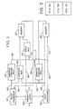
- Figs. 3A, 3B and 3C there is shown a detailed block diagram of the multiprocessor memory access system in which the slow and fast processors are able to access the same stored data in an orderly fashion.
- the slow processor 20 has coupled to it 16 address lines of which 8 address lines indicated by bus 24A are coupled to a decoder 58 at whose input will appear the most significant address bits AB15-AB8 identifying the slow processor 20 and indicating that the slow processor is accessing the memory unit 26.
- the decoder 58 may consist of an inverter and a by-pass switch coupled to each address line with the switch coupled to one input of an 8 input AND gate.
- An example of the decoder 58 that is commercially available is the Texas Instruments 74LS30 8 input NAND gate.
- the other eight address lines indicated as bus 24B will have present thereon the least significant address bits AB7-ABO of the address of the data currently being accessed by the slow processor 20.
- the address bits AB7-ABO are transmitted over the bus 24B to a first in first out address memory unit 22 for storage therein, and also over bus 60 to one input of a 2:1 address multiplexer 34 whose other input receives similar address bits from the fast processor 38 (Fig. 3B) over bus 62.
- the multiplexer 34 will select the address bits generated by the appropriate processor for transmission over bus 64 to the RAM memory unit 26 for use in accessing the data in the memory unit in a manner that is well-known in the art.
- the slow processor 20 (Fig. 3A) will either output or receive 8 data bits DB7-DBO over bus 66.
- the bus 66 is coupled through bus 28 to an 8 bit edge-triggered register 68 for controlling the timing of the output of the data bits DB7-DBO over bus 30 to one input of the 2:1 data multiplexer 32 whose other input is coupled over bus 52 to the common data bus 48 over which appear the data bits DB7-DBO from the fast processor 38 (Fig. 3B).
- the address and the data bits transmitted from one of the processors 20 or 38 will be transmitted into the RAM memory unit 26 during a write operation in a manner that is well-known in the art.
- a read operation of the memory unit 26 (Fig. 3A) by the slow processor 20 occurs, data stored in the memory unit 26 at an address transmitted over bus 64 will be outputted over bus 36 to an 8 bit latch 74 which is selectively enabled to output the eight data bits DB7-DBO over buses 28 and 66 to the processor 20.
- the data bits DB7-DBO are also transmitted over buses 36 and 76 through a buffer driver 78 to the data bus 48 for transmission to the fast processor 38 (Fig. 3B) in a manner that will be described more fully hereinafter.
- the slow processor 20 will output the appropriate read control signal RD over line 80 (Fig. 3A) to initiate a read access operation and a write control signal WR over line 82 to initiate a write access operation.
- Examples of commercially-available circuits that may be used for the elements just disclosed include a Texas Instruments 74LS157 multiplexer, an Intel 2125 1 KX1 RAM memory unit, a Texas Instruments 74LS374 8 bit edge triggered register, a Texas Instruments 74LS373 8 bit fall-through latch, a Texas Instruments 74LS244 buffer driver, and a Fair- child 9403 first-in, first-out buffer memory unit.
- the fast processor 38 which may be a Signetics 8X300 microprocessor to which is coupled an instruction storage unit 84, such as the Signetics 82LS115 PROM which functions, upon receiving the appropriate 9 bit instruction address over bus 86 from the processor 38, to output a 16 bit instruction code over bus 88 to the processor 38, resulting in the operation of the fast processor in accordance with the instruction code in a manner that is well-known in the art.
- an instruction storage unit 84 such as the Signetics 82LS115 PROM which functions, upon receiving the appropriate 9 bit instruction address over bus 86 from the processor 38, to output a 16 bit instruction code over bus 88 to the processor 38, resulting in the operation of the fast processor in accordance with the instruction code in a manner that is well-known in the art.
- an internal communication bus 90 which is coupled to an I/O interface 92, an 8 bit latched port 94 which functions to latch the address bits AB7-ABO generated by the processor 38, a second 8 bit latched port 96 for latching the data bits DB7-DBO being transmitted over bus 46 and a third 8 bit latched port 100 over which various control signals are generated by the processor 38 in a manner that will be described more fully hereinafter.
- the blocks 84, 92, 94, 96 and 100 are standard functional units associated with the fast processor 38 and form no part of the present invention.
- Coupled to the address bus 62 is a second first-in, first-out address storage unit 44 for storing the data addresses generated by the fast processor 3.8 as a result of a conflict with the slow processor 20 for use by the processor 38 in accessing the memory units 26 (Fig. 3A) and 42 (Fig. 3B).
- Coupled to the address bus 62 and the data bus 48 is a second Intel 2125 RAM memory unit 42 which is accessed simultaneously with memory unit 26 (Fig. 3A) by the fast processor 38.
- An output data bus 102 coupled between the RAM memory unit 42 and the data bus 48 allows data to be transmitted over bus 46 to the latched port 96 for subsequent transmission to the processor 38 in a manner that is well-known in the art.
- Figs. 3B and 3C Shown in Figs. 3B and 3C are the priority logic circuits 54 (Fig. 1) for controlling the operation of the multiprocessor system which include four TI 74LS74 D-type flip-flops 104-110 inclusive and three TI 74LS123 single-shot multivibrators 112-116 inclusive for providing the proper pulse width control signals used in enabling the accessing of the memory units 26 (Fig. 3A) and 42 (Fig. 3B) together with conditioning the operation of certain of the priority logic circuits in a manner that will now be disclosed. For purposes of illustration, there will now be described a write operation by the slow processor 20 (Fig. 3A) which involves only the memory unit 26.
- the processor 20 When the processor 20 is in a write mode, the most significant bits of the data address bits will appear on the bus 24A for transmission to the decoder 58 enabling the decoder to output an active high board select signal BRDSEL over line 118 to the D input of flip-flop 104 (Fig. 3C).
- the least significant address bits will appear on bus 24B for storage in the address storage unit 22 upon the generation of an active high write signal WR on the output line 82 of the slow processor 20, which signal is transmitted to the clock input of flip-flop 104 (Fig. 3C).
- the signal WR becomes the signal LOAD (Fig. 3C) over line 120 which signal loads the address bits AB7-ABO into the address storage unit 22.
- the storing of the address bits AB7-ABO in the storage unit 22 loads the address bits into the last slot on the output end of the storage unit 22 and lowers the signal EMPTY appearing on the output line 188 of the storage unit 22 indicating that the storage unit 22 contains an address representing data stored in the memory unit 26.
- the use of a first-in, first-out memory unit for the storage units 22 and 44 implements both the storage of the addresses and keeps track of how many addresses are stored therein, which information is needed by the fast processor 38 to keep the memory units 26 and 42 in balance, as will be described more fully hereinafter.
- the active high write signal WR appearing on the output line 82 of the slow processor 20 will also become the clock signal CLK (Fig. 2C) over line 122 which signal clocks in the data bits DB7-DBO into the 8 bit edge-triggered register 68 (Fig. 3A).
- the signal WR clocks the flip-flop 104 (Fig. 3C) over line 82 on whose D input appears the active high signal BRDSEL as disclosed above.
- Clocking of the flip-flop 104 will output an active high write pending signal WRPD on the Q output of flip-flop 104 for transmission over line 124 to the D input of the synchronizing flip-flop 106 on whose clock input will appear the memory clock signal MCLK over line 126 from the processor 38 (Fig. 3B).
- the flip-flop 106 synchronizes the operation of the processor 38 with the operation of the processor 20 by looking at the clock signal MCLK of the processor 38.
- the signal MCLK is active high when the fast processor 38 is performing any type of access operation such as initiating a write access operation in the memory unit 26 (Fig. 3A) and memory unit 42 (Fig.3B).
- the clocking of the flip-flop 106 (Fig. 3C) by the active high signal MCLK will output the active high signal WRCK on its Q output line 128 to one input of an OR gate 130 which high signal is transmitted from the output of OR gate 130 over line 132 to one input of the AND gate 134.
- the other input to the AND gate 134 is low due to the clock signal MCLK appearing on line 126 being high at this time, indicating an operation of the fast processor 38.
- the active high signal MCLK is transmitted over line 126 through an inverter 136 to the other input of AND gate 134.
- the signal MCLK will go low, at which time the AND gate 134 will output an active high control signal to the one-shot 114 which outputs a pulse WE of predetermined width over line 115 to the memory unit 26 (Fig. 3A) enabling a write operation to occur in the memory unit by the slow processor 20.
- the Q output of flip-flop 106 (Fig. 3C) is also coupled over line 138 to one input of a NOR gate 140.
- NOR gate 140 Upon the write clock signal WRCK going high at the time of a write operation by the slow processor 20, the output of the NOR gate 140 will go low, which signal SEL is transmitted over line 70 to the multiplexers 32 and 34 (Fig. 3A) switching the multiplexers to output the address and data bits generated by the processor 20 over bus 60 and 30, respectively, for transmission to the memory unit 26 to complete the access operation.
- the active high read signal RD will appear on the output line 80 (Fig. 3A) of the processor 20.
- This signal is transmitted over line 80 to the clock input of flip-flop 108 (Fig. 3C) setting the flip-flop, thereby allowing the flip-flop 108 to output an active high read pending signal RDPD over line 141 to the D input of the flip-flop 110, resulting in the flip-flop 110 outputting on its Q output the active high read clock signal RDCK upon the setting of the flip-flop 110 by the signal MCLK going high in the manner described previously.
- the signal RDCK is transmitted over lines 143 and 144 to the latch 74 (Fig.
- the active high signal RDCK is also transmitted over line 143 to the NOR gate 140 (Fig. 3C) whose output low select signal SEL is transmitted over line 70 to the multiplexers 32 and 34 (Fig. 3A) switching the multiplexers to input the address and data bits from the slow processor 20 into the memory unit 26, thereby enabling the processor 20 to perform a read operation.
- the memory unit 26 outputs the required data over bus line 36 to the latch 74 which is enabled by the low RDCK signal transmitted over line 144 in the manner described previously.
- the output signal SEL of the NOR gate 140 is also transmitted over line 70 to the one-shot 116 (Fig. 3C) enabling the one-shot to output over line 117 a pulse of sufficient duration for resetting the flip-flops 104 and 108 ending the pending condition of the slow processor 20.
- the reason for resetting the flip-flops 104 and 108 at this time is to prevent the priority circuits from sensing a double memory access operation by the slow processor 20 due to the length of time required for the processor 20 to complete a memory access operation.
- the flip-flop 110 is clocked to a reset condition by the clock signal MCLK appearing on line 126.
- Fig. 3B there is shown the fast processor 38 coupled to various control units used in the operation of the processor 38 in a manner that is well-known in the art. Included in these units is the PROM memory 84 which stores a fixed program for operating the processor 38.
- the I/O interface 92 functions to couple any I/O device to the processor 38 in a manner that is well-known in the art.
- the 8 bit latched port 94 latches the address bits generated in the processor 38 that are required by the processor 38 in accessing the memory units 26 and 42.
- the address bits are transmitted from the port 94 over the address bus 62 (Figs. 3A and 3B) for inputting into the multiplexer 34, over buses 62 and 150 (Fig. 3B) into the address storage unit 44 and over buses 62 and 40 into the RAM memory unit 42.
- the 8 bit latched port 96 (Fig. 3B) controls the flow of data between the fast processor 38 and the system.
- the latched port 100 outputs the various control signals from the processor 38 for controlling a read or write operation.
- an active high write signal WR appearing on line 152 of the port 100 will enable the one-shot 112 to output the write enable signal WE over line 154 to the RAM memory unit 42 (Fig. 3B) enabling a write access operation to occur in the memory unit in which the data will be outputted from processor 38 to memory unit 42 through port 96 and buses 46 and 48.
- the addresses stored in the address storage unit 44 are those used by the fast processor 38 in attempting to write into the memory unit 26 but failed due to a conflict with the slow processor 20. Since the processor 38 accesses the memory 42 without the possibility of conflict with the processor 20, the raising of the signal WR over line 1 52 enables the access operation of the memory unit 42 to occur. Since both processors are able to access the memory unit 26 (Fig. 3A), the priority circuits will determine which processor has access to the memory unit 26 when there is a conflict in a manner that will now be described.
- an active high write request signal WRREQ will appear on line 156 (Fig. 3B and 3C) of the 8 bit latched port 100, which signal is transmitted to one input of an AND gate 158 (Fig. 3C) and a second AND gate 160 (Fig. 3C).
- the other input of the AND gate 158 is coupled to the output of the NOR gate 140. Since the slow processor 20 (Fig. 3B)
- the fast processor 38 will normally write into both memory units 26 and 42 simultaneously to keep them in balance. Since the processor 38 has complete control of the memory unit 42, the only conflict occurs when both processors 20 and 38 are trying to gain access to the memory unit 26 (Fig. 3A) at the same time. If the fast processor 38 is trying to write into the memory units 26 and 42, the signal WRREQ is raised on line 156 of port 100 (Fig. 3B) as explained previously. This signal is transmitted to one input of the AND gate 160 (Fig. 3C) whose other input is coupled to the output of the NOR gate 140 through an inverter 190.
- the output signal SEL of the NOR gate 140 will be low in the manner described previously, which signal is inverted by the inverter 190 (Fig. 3C) thereby enabling the AND gate 160 to output the active high signal LOAD over line 192 to the address storage unit 44 (Fig. 3B) storing the address the processor 38 was attempting to write into the memory unit 26 (Fig. 3A).
- the signal SEL going low will switch the multiplexers 32 and 34 (Fig. 3A) enabling the processor 20 to access the memory unit 26 (Fig. 3A). Switching of the multiplexers 32 and 34 in this manner interrupts the write operation of the memory unit 26 by the processor 38 requiring the processor 38 to balance the memory units 26 and 42 at the conclusion of the operation of the processor 20.
- the storing of the address in the address storage unit 44 upon the raising of the signal LOAD on line 192 in the manner described above will lower the signal EMPTY.
- the fast processor 38 checking the output bus 167 of the driver 166 (Fig. 3B) and seeing the low output signal of the driver appearing on the line corresponding to the input line 174 of the driver 166, the processor 38 will initiate a balancing operation in which the addresses stored in the address storage unit 44 are used to balance the memory unit 26.
- the fast processor 38 (Fig. 3B) which occurs when the memory unit 26 contains data not found in memory unit 42.
- the processor 38 is required to keep the data stored in both memory units 26 and 42 balanced.
- the processor 38 is programmed to check the address storage units 22 and 44 to see if they are storing any addresses therein indicating that their associated memory units contain data not stored in the other memory unit. This condition will occur when the slow processor 20 writes into the memory unit 26 or when the fast processor 38 is interrupted during a write operation of both memory units 26 and 42 by the operation of the processor 20 in a manner to be described hereinafter.
- the fast processor 38 is required to transfer data between the memory units so that they are in balance. This operation is called a balancing operation.
- the fast processor 38 (Fig. 3B) will initiate a balancing operation by raising an active high signal ENBL on the output line 164 of the latched port 100 which signal is transmitted to the buffer driver 166 (Fig. 3B) on whose input lines appear the signal EMPTY received over lines 188 and 174 from the address storage units 22 (Fig. 3A) and 44 (Fig. 3B) respectively.
- the signal EMPTY indicates whether any addresses are stored in the storage units indicating an out of balance condition exists. If the EMPTY signal appearing on the corresponding lines of the output bus 167 is low, the output signals of the driver 166 will be low.
- the EMPTY signal appearing on the output line 174 of the storage unit 44 is low. This signal is transmitted over buses 48 and 46 to the port 96 which transmits the signal to the processor 38.
- the processor 38 will initiate a balancing operation by raising the active high signal OE on the line 169 of port 100 (Fig. 3B) which signal is transmitted to the address storage unit 44 resulting in an address being outputted over the buses 170, 48 and 46 to the processor 38.
- the raising of the signal OE over line 169 puts the address on the bus 170 while the signal DUMP eliminates the signal from the bus 170 at the completion of the balancing operation.
- the processor 38 using the address received will output an enable signal OE over line 172 of the latched port 100 to the memory unit 42 allowing the processor 38 to read the data from the memory unit 42.
- the processor 38 will then write the data into the memory unit 26 by raising the write request signal WRREQ on line 156 of port 100 for transmission to the priority circuits in the manner described previously.
- the write enable signal WE will be raised on the output line 115 (Fig. 3C) of the one-shot 114 enabling the data to be written into the memory unit 26. This operation is repeated until the signal EMPTY on the output line 174 of the storage memory unit 44 is raised indicating that all the addresses contained in the storage unit have been processed.
- the fast processor 38 raises the read request signal RDREQ on the output line 176 (Fig. 3B and 3C) of the latched port 100 for transmission to one input of the AND gate 178 (Fig. 3C).
- the other input of the AND gate 178 is coupled to the output of the NOR gate 140. If the slow processor 20 is not contending at this time, the output of the NOR gate 140 will be high, enabling the AND gate 178 to output the active high signal DUMP over line 180 to the address storage register 22 (Fig. 3A) which outputs the address present at its output over buses 182 (Fig.
- the slow processor If during the balancing operation, the slow processor generates a write operation an AND gate 193 (Fig. 3C) whose inputs are coupled to line 176 and the output of the inverter 190 will output the active high signal LOAD over line 120 to the storage unit 22 (Fig. 3A) allowing the address at which the processor 20 was writing to be stored.
- the processor 38 After reading out the data from the memory unit 26, the processor 38 will write the data into the memory unit 42 by raising the enable signal ENBL over the output line 184 of the latched port 100. This signal is transmitted to the buffer driver 78 (Fig. 3A) which outputs the data present on the bus 36 to the bus 48. The data appearing on bus 48 is written into the memory unit 42 (Fig. 3B) upon the write enable signal WE appearing on the output line 154 of the one-shot 112 (Fig. 3B) as a result of the raising of the write signal WR on the output line 152 of the port 100. This operation will be repeated for each address appearing on the output of the address storage register 22 (Fig. 3A) until the signal EMPTY appearing on the output line 188 of the storage unit 22 is raised.
- This signal is transmitted to the buffer driver 166 indicating the condition of the storage unit 22. If at this time both address storage units 22 (Fig. 3A) and 44 (Fig. 3B) are empty indicating that the memory units 26 and 42 are in balance, the balancing operation will be terminated by the fast processor 38.
- both memory units 26 and 42 are continuously updated and balanced by the fast processor 38, enabling both the slow processor 20 and the fast processor 38 to perform access operations with a minimum of interference and without danger of losing data when conflicts do occur.
Landscapes
- Engineering & Computer Science (AREA)
- Theoretical Computer Science (AREA)
- Physics & Mathematics (AREA)
- General Engineering & Computer Science (AREA)
- General Physics & Mathematics (AREA)
- Multi Processors (AREA)
- Bus Control (AREA)
Abstract
Claims (2)
Applications Claiming Priority (2)
| Application Number | Priority Date | Filing Date | Title |
|---|---|---|---|
| US06/003,692 US4282572A (en) | 1979-01-15 | 1979-01-15 | Multiprocessor memory access system |
| US3692 | 1979-01-15 |
Publications (3)
| Publication Number | Publication Date |
|---|---|
| EP0022829A1 EP0022829A1 (fr) | 1981-01-28 |
| EP0022829A4 EP0022829A4 (fr) | 1981-08-28 |
| EP0022829B1 true EP0022829B1 (fr) | 1984-04-11 |
Family
ID=21707114
Family Applications (1)
| Application Number | Title | Priority Date | Filing Date |
|---|---|---|---|
| EP80900229A Expired EP0022829B1 (fr) | 1979-01-15 | 1980-07-29 | Systeme de traitement de donnees |
Country Status (5)
| Country | Link |
|---|---|
| US (1) | US4282572A (fr) |
| EP (1) | EP0022829B1 (fr) |
| JP (1) | JPS55501115A (fr) |
| DE (1) | DE3067401D1 (fr) |
| WO (1) | WO1980001521A1 (fr) |
Families Citing this family (27)
| Publication number | Priority date | Publication date | Assignee | Title |
|---|---|---|---|---|
| SE430733B (sv) * | 1980-03-24 | 1983-12-05 | Ellemtel Utvecklings Ab | Sett och anordning for att under pagaende drift spara fel i ett berekningsforlopp |
| JPS6037938B2 (ja) * | 1980-12-29 | 1985-08-29 | 富士通株式会社 | 情報処理装置 |
| US4541045A (en) * | 1981-09-21 | 1985-09-10 | Racal-Milgo, Inc. | Microprocessor architecture employing efficient operand and instruction addressing |
| US4449182A (en) * | 1981-10-05 | 1984-05-15 | Digital Equipment Corporation | Interface between a pair of processors, such as host and peripheral-controlling processors in data processing systems |
| US4823256A (en) * | 1984-06-22 | 1989-04-18 | American Telephone And Telegraph Company, At&T Bell Laboratories | Reconfigurable dual processor system |
| JPS6143345A (ja) * | 1984-08-07 | 1986-03-01 | Nec Corp | メモリ装置 |
| JPS61166668A (ja) * | 1985-01-19 | 1986-07-28 | Panafacom Ltd | 多重プロセツサ制御方式 |
| US4868738A (en) * | 1985-08-15 | 1989-09-19 | Lanier Business Products, Inc. | Operating system independent virtual memory computer system |
| CA1270338A (fr) * | 1985-09-11 | 1990-06-12 | Akihiko Hoshino | Systeme de traitement de donnees pour unites de traitement a debits differents |
| FR2611396B1 (fr) * | 1987-02-27 | 1991-10-11 | Trt Telecom Radio Electr | Dispositif pour permettre a deux systemes de traitement d'informations l'acces a un circuit commun |
| AU1682188A (en) * | 1987-04-02 | 1988-11-02 | Stellar Computer Inc. | Dynamically assignable shared register sets |
| US4933846A (en) * | 1987-04-24 | 1990-06-12 | Network Systems Corporation | Network communications adapter with dual interleaved memory banks servicing multiple processors |
| JPH01303543A (ja) * | 1988-05-31 | 1989-12-07 | Fujitsu Ltd | メモリアクセス制御装置 |
| DE68924306T2 (de) * | 1988-06-27 | 1996-05-09 | Digital Equipment Corp | Mehrprozessorrechneranordnungen mit gemeinsamem Speicher und privaten Cache-Speichern. |
| US4980819A (en) * | 1988-12-19 | 1990-12-25 | Bull Hn Information Systems Inc. | Mechanism for automatically updating multiple unit register file memories in successive cycles for a pipelined processing system |
| US5222224A (en) * | 1989-02-03 | 1993-06-22 | Digital Equipment Corporation | Scheme for insuring data consistency between a plurality of cache memories and the main memory in a multi-processor system |
| JPH03210649A (ja) * | 1990-01-12 | 1991-09-13 | Fujitsu Ltd | マイクロコンピュータおよびそのバスサイクル制御方法 |
| US5247636A (en) * | 1990-05-31 | 1993-09-21 | International Business Machines Corporation | Digital processor clock circuit |
| US5835953A (en) * | 1994-10-13 | 1998-11-10 | Vinca Corporation | Backup system that takes a snapshot of the locations in a mass storage device that has been identified for updating prior to updating |
| US5649152A (en) * | 1994-10-13 | 1997-07-15 | Vinca Corporation | Method and system for providing a static snapshot of data stored on a mass storage system |
| US5708813A (en) * | 1994-12-12 | 1998-01-13 | Digital Equipment Corporation | Programmable interrupt signal router |
| JP3123413B2 (ja) * | 1995-11-07 | 2001-01-09 | 株式会社日立製作所 | コンピュータシステム |
| US5907862A (en) * | 1996-07-16 | 1999-05-25 | Standard Microsystems Corp. | Method and apparatus for the sharing of a memory device by multiple processors |
| GB2331379A (en) * | 1997-11-13 | 1999-05-19 | Advanced Telecommunications Mo | Controlling access to a shared memory by dual mapping |
| JP4624715B2 (ja) * | 2004-05-13 | 2011-02-02 | ルネサスエレクトロニクス株式会社 | システムlsi |
| KR101192938B1 (ko) * | 2007-09-14 | 2012-10-18 | 후지쯔 가부시끼가이샤 | 정보 처리 장치 및 그 제어 방법 |
| US8914612B2 (en) | 2007-10-29 | 2014-12-16 | Conversant Intellectual Property Management Inc. | Data processing with time-based memory access |
Family Cites Families (17)
| Publication number | Priority date | Publication date | Assignee | Title |
|---|---|---|---|---|
| DE1549397B2 (de) * | 1967-06-16 | 1972-09-14 | Chemische Werke Hüls AG, 4370 Mari | Verfahren zur automatischen steuerung chemischer anlagen |
| US3866182A (en) * | 1968-10-17 | 1975-02-11 | Fujitsu Ltd | System for transferring information between memory banks |
| US3581291A (en) * | 1968-10-31 | 1971-05-25 | Hitachi Ltd | Memory control system in multiprocessing system |
| US3591291A (en) * | 1969-05-26 | 1971-07-06 | Conductron Corp | Method and apparatus for sensing reflected light and diffused light from a surface to indicate the roughness of said surface |
| US3665487A (en) * | 1969-06-05 | 1972-05-23 | Honeywell Inf Systems | Storage structure for management control subsystem in multiprogrammed data processing system |
| US3771137A (en) * | 1971-09-10 | 1973-11-06 | Ibm | Memory control in a multipurpose system utilizing a broadcast |
| US3950729A (en) * | 1973-08-31 | 1976-04-13 | Nasa | Shared memory for a fault-tolerant computer |
| US3845474A (en) * | 1973-11-05 | 1974-10-29 | Honeywell Inf Systems | Cache store clearing operation for multiprocessor mode |
| US3889237A (en) * | 1973-11-16 | 1975-06-10 | Sperry Rand Corp | Common storage controller for dual processor system |
| US4050058A (en) * | 1973-12-26 | 1977-09-20 | Xerox Corporation | Microprocessor with parallel operation |
| US3896419A (en) * | 1974-01-17 | 1975-07-22 | Honeywell Inf Systems | Cache memory store in a processor of a data processing system |
| US3979726A (en) * | 1974-04-10 | 1976-09-07 | Honeywell Information Systems, Inc. | Apparatus for selectively clearing a cache store in a processor having segmentation and paging |
| US4020466A (en) * | 1974-07-05 | 1977-04-26 | Ibm Corporation | Memory hierarchy system with journaling and copy back |
| US3964054A (en) * | 1975-06-23 | 1976-06-15 | International Business Machines Corporation | Hierarchy response priority adjustment mechanism |
| US4034347A (en) * | 1975-08-08 | 1977-07-05 | Bell Telephone Laboratories, Incorporated | Method and apparatus for controlling a multiprocessor system |
| US4084231A (en) * | 1975-12-18 | 1978-04-11 | International Business Machines Corporation | System for facilitating the copying back of data in disc and tape units of a memory hierarchial system |
| US4040023A (en) * | 1975-12-22 | 1977-08-02 | Bell Telephone Laboratories, Incorporated | Recorder transfer arrangement maintaining billing data continuity |
-
1979
- 1979-01-15 US US06/003,692 patent/US4282572A/en not_active Expired - Lifetime
-
1980
- 1980-01-11 WO PCT/US1980/000024 patent/WO1980001521A1/fr not_active Ceased
- 1980-01-11 DE DE8080900229T patent/DE3067401D1/de not_active Expired
- 1980-01-11 JP JP50038580A patent/JPS55501115A/ja active Pending
- 1980-07-29 EP EP80900229A patent/EP0022829B1/fr not_active Expired
Also Published As
| Publication number | Publication date |
|---|---|
| EP0022829A1 (fr) | 1981-01-28 |
| JPS55501115A (fr) | 1980-12-11 |
| WO1980001521A1 (fr) | 1980-07-24 |
| DE3067401D1 (en) | 1984-05-17 |
| EP0022829A4 (fr) | 1981-08-28 |
| US4282572A (en) | 1981-08-04 |
Similar Documents
| Publication | Publication Date | Title |
|---|---|---|
| EP0022829B1 (fr) | Systeme de traitement de donnees | |
| EP0090575B1 (fr) | Système de mémoire | |
| US4698753A (en) | Multiprocessor interface device | |
| US3728693A (en) | Programmatically controlled interrupt system for controlling input/output operations in a digital computer | |
| US4991079A (en) | Real-time data processing system | |
| CA1290073C (fr) | Memoire d'attente en file pour donnees extraites | |
| EP0288649A1 (fr) | Système de commande de mémoire | |
| US5249284A (en) | Method and system for maintaining data coherency between main and cache memories | |
| US4811202A (en) | Quadruply extended time multiplexed information bus for reducing the `pin out` configuration of a semiconductor chip package | |
| US4347567A (en) | Computer system apparatus for improving access to memory by deferring write operations | |
| GB2148563A (en) | Multiprocessor system | |
| JPS6244303B2 (fr) | ||
| JPH04306748A (ja) | 情報処理装置 | |
| US5060186A (en) | High-capacity memory having extended addressing capacity in a multiprocessing system | |
| US5353416A (en) | CPU lock logic for corrected operation with a posted write array | |
| EP0509994B1 (fr) | Table centralisee de modification et de reference pour systeme de memoire virtuelle d'un multicalculateur | |
| US6415361B1 (en) | Apparatus for controlling cache by using dual-port transaction buffers | |
| US5089953A (en) | Control and arbitration unit | |
| US5408612A (en) | Microprocessor system for selectively accessing a processor internal register when the processor has control of the bus and partial address identifying the register | |
| US5699553A (en) | Memory accessing device for a pipeline information processing system | |
| JPH0427583B2 (fr) | ||
| KR100278805B1 (ko) | 멀티 프로세싱 시스템의 데이터 중재장치 및 방법 | |
| KR0171771B1 (ko) | 컴퓨터 시스템에 있어서 어드레스 버스 잠금 제어장치 | |
| EP0460852A2 (fr) | Système de maintien de la cohérence des données entre mémoire principale et antémémoire | |
| JPS63266572A (ja) | デ−タ処理システム |
Legal Events
| Date | Code | Title | Description |
|---|---|---|---|
| PUAI | Public reference made under article 153(3) epc to a published international application that has entered the european phase |
Free format text: ORIGINAL CODE: 0009012 |
|
| AK | Designated contracting states |
Designated state(s): DE FR GB |
|
| DET | De: translation of patent claims | ||
| 17P | Request for examination filed |
Effective date: 19810112 |
|
| GRAA | (expected) grant |
Free format text: ORIGINAL CODE: 0009210 |
|
| AK | Designated contracting states |
Designated state(s): DE FR GB |
|
| REF | Corresponds to: |
Ref document number: 3067401 Country of ref document: DE Date of ref document: 19840517 |
|
| ET | Fr: translation filed | ||
| PGFP | Annual fee paid to national office [announced via postgrant information from national office to epo] |
Ref country code: DE Payment date: 19850206 Year of fee payment: 6 |
|
| PLBE | No opposition filed within time limit |
Free format text: ORIGINAL CODE: 0009261 |
|
| STAA | Information on the status of an ep patent application or granted ep patent |
Free format text: STATUS: NO OPPOSITION FILED WITHIN TIME LIMIT |
|
| 26N | No opposition filed | ||
| GBPC | Gb: european patent ceased through non-payment of renewal fee | ||
| PG25 | Lapsed in a contracting state [announced via postgrant information from national office to epo] |
Ref country code: FR Free format text: LAPSE BECAUSE OF NON-PAYMENT OF DUE FEES Effective date: 19870930 |
|
| PG25 | Lapsed in a contracting state [announced via postgrant information from national office to epo] |
Ref country code: DE Effective date: 19871001 |
|
| REG | Reference to a national code |
Ref country code: FR Ref legal event code: ST |
|
| PG25 | Lapsed in a contracting state [announced via postgrant information from national office to epo] |
Ref country code: GB Effective date: 19881118 |