EP0023294A2 - Verfahren zum Reparieren integrierter Schaltungen - Google Patents
Verfahren zum Reparieren integrierter Schaltungen Download PDFInfo
- Publication number
- EP0023294A2 EP0023294A2 EP80103965A EP80103965A EP0023294A2 EP 0023294 A2 EP0023294 A2 EP 0023294A2 EP 80103965 A EP80103965 A EP 80103965A EP 80103965 A EP80103965 A EP 80103965A EP 0023294 A2 EP0023294 A2 EP 0023294A2
- Authority
- EP
- European Patent Office
- Prior art keywords
- dielectric layer
- pattern
- opens
- lines
- conductor
- Prior art date
- Legal status (The legal status is an assumption and is not a legal conclusion. Google has not performed a legal analysis and makes no representation as to the accuracy of the status listed.)
- Granted
Links
Images


Classifications
-
- H—ELECTRICITY
- H10—SEMICONDUCTOR DEVICES; ELECTRIC SOLID-STATE DEVICES NOT OTHERWISE PROVIDED FOR
- H10W—GENERIC PACKAGES, INTERCONNECTIONS, CONNECTORS OR OTHER CONSTRUCTIONAL DETAILS OF DEVICES COVERED BY CLASS H10
- H10W99/00—Subject matter not provided for in other groups of this subclass
-
- H—ELECTRICITY
- H05—ELECTRIC TECHNIQUES NOT OTHERWISE PROVIDED FOR
- H05K—PRINTED CIRCUITS; CASINGS OR CONSTRUCTIONAL DETAILS OF ELECTRIC APPARATUS; MANUFACTURE OF ASSEMBLAGES OF ELECTRICAL COMPONENTS
- H05K3/00—Apparatus or processes for manufacturing printed circuits
- H05K3/22—Secondary treatment of printed circuits
- H05K3/225—Correcting or repairing of printed circuits
-
- H—ELECTRICITY
- H10—SEMICONDUCTOR DEVICES; ELECTRIC SOLID-STATE DEVICES NOT OTHERWISE PROVIDED FOR
- H10W—GENERIC PACKAGES, INTERCONNECTIONS, CONNECTORS OR OTHER CONSTRUCTIONAL DETAILS OF DEVICES COVERED BY CLASS H10
- H10W20/00—Interconnections in chips, wafers or substrates
- H10W20/01—Manufacture or treatment
- H10W20/031—Manufacture or treatment of conductive parts of the interconnections
- H10W20/067—Manufacture or treatment of conductive parts of the interconnections by modifying the pattern of conductive parts
-
- H—ELECTRICITY
- H10—SEMICONDUCTOR DEVICES; ELECTRIC SOLID-STATE DEVICES NOT OTHERWISE PROVIDED FOR
- H10W—GENERIC PACKAGES, INTERCONNECTIONS, CONNECTORS OR OTHER CONSTRUCTIONAL DETAILS OF DEVICES COVERED BY CLASS H10
- H10W20/00—Interconnections in chips, wafers or substrates
- H10W20/40—Interconnections external to wafers or substrates, e.g. back-end-of-line [BEOL] metallisations or vias connecting to gate electrodes
- H10W20/49—Adaptable interconnections, e.g. fuses or antifuses
-
- H—ELECTRICITY
- H05—ELECTRIC TECHNIQUES NOT OTHERWISE PROVIDED FOR
- H05K—PRINTED CIRCUITS; CASINGS OR CONSTRUCTIONAL DETAILS OF ELECTRIC APPARATUS; MANUFACTURE OF ASSEMBLAGES OF ELECTRICAL COMPONENTS
- H05K2203/00—Indexing scheme relating to apparatus or processes for manufacturing printed circuits covered by H05K3/00
- H05K2203/17—Post-manufacturing processes
- H05K2203/173—Adding connections between adjacent pads or conductors, e.g. for modifying or repairing
-
- H—ELECTRICITY
- H05—ELECTRIC TECHNIQUES NOT OTHERWISE PROVIDED FOR
- H05K—PRINTED CIRCUITS; CASINGS OR CONSTRUCTIONAL DETAILS OF ELECTRIC APPARATUS; MANUFACTURE OF ASSEMBLAGES OF ELECTRICAL COMPONENTS
- H05K2203/00—Indexing scheme relating to apparatus or processes for manufacturing printed circuits covered by H05K3/00
- H05K2203/17—Post-manufacturing processes
- H05K2203/175—Configurations of connections suitable for easy deletion, e.g. modifiable circuits or temporary conductors for electroplating; Processes for deleting connections
-
- H—ELECTRICITY
- H05—ELECTRIC TECHNIQUES NOT OTHERWISE PROVIDED FOR
- H05K—PRINTED CIRCUITS; CASINGS OR CONSTRUCTIONAL DETAILS OF ELECTRIC APPARATUS; MANUFACTURE OF ASSEMBLAGES OF ELECTRICAL COMPONENTS
- H05K3/00—Apparatus or processes for manufacturing printed circuits
- H05K3/46—Manufacturing multilayer circuits
- H05K3/4685—Manufacturing of cross-over conductors
Definitions
- This invention relates to the repair of integrated circuits, particularly to the repair of opens and shorts in the metallurgy of multilevel devices.
- Fine line conductors present a particular problem in that discontinuities or shorts in conductor runs or shorts between conductor lines occur. They can be caused,for example, by the presence of pin-holes in resists employed for photolithographic delineation of the conductor patterns. This results in the rejection of circuits with attendant decrease in yield and increased cost. With the projected high densification of conductor patterns, the present fabrication processes are incapable of being economically employed for repairing the defective (e.g. shorted and/or open) conductors for purposes of reclaiming the devices.
- a repair technique for eliminating discontinuities in metallization patterns is disclosed in IBM Technical Disclosure Bulletin, Vol. 20, No. 4, September 1977, page 1596. However, the method disclosed there is adapted to gas panels. Also, it does not provide a repair opportunity for shorts between conductors.
- the invention as claimed intends to provide a remedy.
- the novel technique for repair of opens and shorts in integrated circuits consists of a sequence of steps which isolate the defective line section(s) and bridge the ends of the perfect lines.
- all shorted conductor lines are converted into opens by appropriate severing of the conductor lines below and above the shorted portions so as to isolate the shorted portion as a non-functional island.
- the modified conductor pattern is overcoated with an appropriate dielectric layer (e.g. quartz, polyimide, silicon dioxide, silicon nitride, or combination thereof) in sufficient thickness to provide the desired insulation and/or passivation.
- the dielectric layers can be applied in a portion normally half the thickness required by the specification anticipating insulation of superposed conductor patterns.
- via holes are formed in the dielectric layer to expose the terminal portions of the underlying conductor pattern at all points adjacent all opens.
- dielectric layer with the conductor metal, and delineating patch lines over all opens, including all shorted areas.
- Another dielectric layer can then be formed, e.g. by a blanket coating, over the conductive patch lines and the dielectric layer, which, when employed, can comprise the remaining half or portion of the specification thickness required for insulation of overlying conductive patterns.
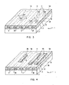
- Fig. 1 shows a portion of an integrated circuit 1 which will normally have P- and N-type regions providing active and passive components of conventional integrated circuit such, for example, as described in U.S. Patents No. 3,539,876 and No. 4,076,575.
- the active and passive regions in substrate 2 have not been shown since they are not significant for this invention.
- Substrate 2 is covered with a passivating dielectric or insulating layer 3 which may be made of any of conventional materials such as quartz, polyimide, silicon dioxide, silicon nitride, or a composite of silicon nitride over silicon dioxide.
- the structures being described, unless otherwise noted, are conventional integrated circuit structures which may be fabricated by methods known in the art, e.g. U.S. Patent No. 3,539,876.
- the dielectric or insulating layer 3 is a compositve of a 1000 I thick bottom layer of silicon dioxide covered with a layer of silicon nitride 1600 ⁇ in thickness.
- a first level metallization pattern 4 is formed over the surface of the dielectric layer 3.
- This metallization pattern which may be of a thickness of 0.85 microns, may also be of any conventional metal used in integrated circuit or electronic package fabrication.
- the metallization can comprise aluminum and copper alloys thereof which can be applied by any technique such as those described in said U.S. Patent 3,539,876.
- the deposition may be, for example, vapor deposition or R.F. sputter or electro or electroless plated deposition.
- the metallization can be formed as a blanket coating which can be delineated into the desired pattern by photolithographic techniques.
- the metallization can comprise complex and intricate patterns, however, for purposes of simplifying the description of this invention, the metallization pattern is shown as a series of conductor runs or lines 5.
- the widths 6 of the runs can be about 25 microns or less with a spacing 7 of about 3 microns between them.
- the metallization pattern in configurations normally employed for-integrated circuits and their package will include connections to various regions in substrate 2-by contacts passing through the dielectric layer 3. These have not been shown since it would not aid in the illustration of the present invention.
- a blanket layer of a dielectric 10 in a thickness which can comprise a portion, preferably half of the specification thickness required for insulation in the formation of overlying conductor pattern of a multilayered conductor structure.
- This dielectric can be formed by any of the deposition techniques described in said U.S. Patent 3,539,876, for example, by chemical vapor deposition as well as spraying, cathode sputtering or R.F. sputtering methods.
- This layer 10 can be of conventional materials such as silicon nitride, aluminum oxide, polyimide or silicon dioxide, as well as composites thereof.
- the layer comprises a 2-8 micron thick layer of R.F. sputter deposited silicon dioxide.
- via holes 11 are formed, e.g. etched through dielectric layer 10 to expose portions at the terminal ends 5A of the desired basic conductor pattern 4 adjacent all opens 8 and 9A,
- the photoresist is removed, and the dielectric blanket coated with a conductive metal layer as noted above, in a minimum thickness sufficient for conductivity, e.g. about 1-2 microns.
- This conductive layer is then delineated by photolithographic techniques into conductive patch lines 8B bridging open 8, and into conductive patch lines 9B bridging opens 9A and spanning over the isolated shorted portion 16.
- One effective technique for delineating the patch lines is by E-beam lithography under computer control utilizing programmed location data observed and recorded for the original opens and shorts.
- a dielectric layer 17 is coated over the substrate to the thickness required for insulation.
- the thickness of the final dielectric layer 17 can be the remaining thickness (e.g. 1-4 microns) required for insulation.
- the dielectric layer 17 can be any of the conventional materials, applied by any conventional technique as discussed above. It may be noted that since the dielectric layers 10 and 17 were applied in two coats, there is an accompanying advantage in the minimization of the possibility of the occurrence of interplane pin-holes.
- processing of the substrate can proceed in conventional manner, which can include the completion of multilayer metallization, which, for simplicity, has been illustrated as comprised of merely transverse conductor runs 20 interconnected to the underlying conductor pattern 4 (inclusive of patch lines 8B and 9B) through via connectors 21.
Landscapes
- Engineering & Computer Science (AREA)
- Manufacturing & Machinery (AREA)
- Microelectronics & Electronic Packaging (AREA)
- Internal Circuitry In Semiconductor Integrated Circuit Devices (AREA)
- Production Of Multi-Layered Print Wiring Board (AREA)
Applications Claiming Priority (2)
| Application Number | Priority Date | Filing Date | Title |
|---|---|---|---|
| US61951 | 1979-07-30 | ||
| US06/061,951 US4259367A (en) | 1979-07-30 | 1979-07-30 | Fine line repair technique |
Publications (3)
| Publication Number | Publication Date |
|---|---|
| EP0023294A2 true EP0023294A2 (de) | 1981-02-04 |
| EP0023294A3 EP0023294A3 (en) | 1983-08-31 |
| EP0023294B1 EP0023294B1 (de) | 1985-06-12 |
Family
ID=22039231
Family Applications (1)
| Application Number | Title | Priority Date | Filing Date |
|---|---|---|---|
| EP80103965A Expired EP0023294B1 (de) | 1979-07-30 | 1980-07-10 | Verfahren zum Reparieren integrierter Schaltungen |
Country Status (6)
| Country | Link |
|---|---|
| US (1) | US4259367A (de) |
| EP (1) | EP0023294B1 (de) |
| JP (1) | JPS5621347A (de) |
| CA (1) | CA1139018A (de) |
| DE (1) | DE3070754D1 (de) |
| IT (1) | IT1151015B (de) |
Cited By (3)
| Publication number | Priority date | Publication date | Assignee | Title |
|---|---|---|---|---|
| GB2169446A (en) * | 1985-01-07 | 1986-07-09 | Motorola Inc | Integrated circuit multilevel metallization and method for making same |
| DE19721310C2 (de) * | 1996-05-22 | 2003-04-03 | Advantest Corp | Verfahren zum Reparieren eines Halbleiterspeichers |
| EP4383958A1 (de) * | 2022-12-08 | 2024-06-12 | Airbus SAS | Bauteil mit einer schicht, die mindestens eine leiterplatte mit anschlussanschlüssen umfasst, verfahren zur reparatur eines solchen bauteils und repariertes teil |
Families Citing this family (53)
| Publication number | Priority date | Publication date | Assignee | Title |
|---|---|---|---|---|
| JPS5772234A (en) * | 1980-10-20 | 1982-05-06 | Matsushita Electric Ind Co Ltd | Production of electrode structure |
| US4810663A (en) * | 1981-12-07 | 1989-03-07 | Massachusetts Institute Of Technology | Method of forming conductive path by low power laser pulse |
| JPS59168652A (ja) * | 1983-03-16 | 1984-09-22 | Hitachi Ltd | 素子修正方法及びその装置 |
| US4594471A (en) * | 1983-07-13 | 1986-06-10 | Semiconductor Energy Laboratory Co., Ltd. | Photoelectric conversion device |
| US4713518A (en) * | 1984-06-08 | 1987-12-15 | Semiconductor Energy Laboratory Co., Ltd. | Electronic device manufacturing methods |
| US4665295A (en) * | 1984-08-02 | 1987-05-12 | Texas Instruments Incorporated | Laser make-link programming of semiconductor devices |
| JPS6130672A (ja) * | 1984-07-23 | 1986-02-12 | Hitachi Ltd | 選択的加工方法 |
| US4924287A (en) * | 1985-01-20 | 1990-05-08 | Avner Pdahtzur | Personalizable CMOS gate array device and technique |
| JPS61202454A (ja) * | 1985-03-05 | 1986-09-08 | Mitsubishi Electric Corp | アルミニウム配線の被切断回路の構造と切断方法 |
| JPH0740101B2 (ja) * | 1985-04-23 | 1995-05-01 | 旭硝子株式会社 | 薄膜トランジスタ |
| US4674176A (en) * | 1985-06-24 | 1987-06-23 | The United States Of America As Represented By The United States Department Of Energy | Planarization of metal films for multilevel interconnects by pulsed laser heating |
| US4681795A (en) * | 1985-06-24 | 1987-07-21 | The United States Of America As Represented By The Department Of Energy | Planarization of metal films for multilevel interconnects |
| JPH0763064B2 (ja) * | 1986-03-31 | 1995-07-05 | 株式会社日立製作所 | Ic素子における配線接続方法 |
| US4683652A (en) * | 1986-08-22 | 1987-08-04 | Hatfield Jerry L | Printed circuit repair process |
| IL82113A (en) * | 1987-04-05 | 1992-08-18 | Zvi Orbach | Fabrication of customized integrated circuits |
| JP2698357B2 (ja) * | 1987-08-17 | 1998-01-19 | キヤノン株式会社 | 電極間の短絡部分離法及び液晶パネルの製造法 |
| JP2594972B2 (ja) * | 1987-09-11 | 1997-03-26 | 株式会社日立製作所 | 配線形成方法およびその装置 |
| JPH0680662B2 (ja) * | 1987-12-02 | 1994-10-12 | 株式会社日立製作所 | Ic素子の修正方法 |
| US4849363A (en) * | 1988-03-18 | 1989-07-18 | Digital Equipment Corporation | Integrated circuit having laser-alterable metallization layer |
| US4908938A (en) * | 1988-05-26 | 1990-03-20 | Siemens Aktiengesellschaft | Method for repairing interconnect interruptions by bridging with congruent preforms |
| US5171709A (en) * | 1988-07-25 | 1992-12-15 | International Business Machines Corporation | Laser methods for circuit repair on integrated circuits and substrates |
| US5182230A (en) * | 1988-07-25 | 1993-01-26 | International Business Machines Corporation | Laser methods for circuit repair on integrated circuits and substrates |
| US4919971A (en) * | 1988-09-23 | 1990-04-24 | International Business Machines Corporation | Self-induced repairing of conductor lines |
| US4880959A (en) * | 1988-10-26 | 1989-11-14 | International Business Machines Corporation | Process for interconnecting thin-film electrical circuits |
| US4974048A (en) * | 1989-03-10 | 1990-11-27 | The Boeing Company | Integrated circuit having reroutable conductive paths |
| JP2567952B2 (ja) * | 1989-09-05 | 1996-12-25 | 株式会社日立製作所 | Lsi補修配線方法 |
| US4994154A (en) * | 1990-02-06 | 1991-02-19 | International Business Machines Corporation | High frequency electrochemical repair of open circuits |
| US5077891A (en) * | 1990-04-30 | 1992-01-07 | Ag Communication Systems Corporation | Method for reconstructing the conductor traces of a printed circuit board assembly |
| JP2731288B2 (ja) * | 1990-08-28 | 1998-03-25 | 株式会社日立製作所 | 多層配線方法 |
| US5060370A (en) * | 1990-10-15 | 1991-10-29 | Scales Jr James W | Modification method for etched printed circuit boards |
| US5153408A (en) * | 1990-10-31 | 1992-10-06 | International Business Machines Corporation | Method and structure for repairing electrical lines |
| US5288007A (en) * | 1991-10-04 | 1994-02-22 | International Business Machine Corporation | Apparatus and methods for making simultaneous electrical connections |
| US5193732A (en) * | 1991-10-04 | 1993-03-16 | International Business Machines Corporation | Apparatus and methods for making simultaneous electrical connections |
| US5391516A (en) * | 1991-10-10 | 1995-02-21 | Martin Marietta Corp. | Method for enhancement of semiconductor device contact pads |
| US5455461A (en) * | 1992-09-21 | 1995-10-03 | Fujitsu Limited | Semiconductor device having reformed pad |
| JPH06110069A (ja) * | 1992-09-29 | 1994-04-22 | Matsushita Electric Ind Co Ltd | 電子部品の欠陥修復方法および欠陥修復装置 |
| DE4316964C2 (de) * | 1993-02-27 | 2002-01-31 | Saint Gobain Sekurit D Gmbh | Verfahren zur Herstellung einer heizbaren Verbundglasscheibe mit in der thermoplastischen Zwischenschicht angeordneten Metalldrähten und Verwendung einer elektronischen Schaltung zur Durchführung des Verfahrens |
| US5532853A (en) * | 1993-03-04 | 1996-07-02 | Samsung Electronics Co., Ltd. | Reparable display device matrix for repairing the electrical connection of a bonding pad to its associated signal line |
| JPH06302603A (ja) * | 1993-03-26 | 1994-10-28 | Hitachi Ltd | Ic素子 |
| JPH06283534A (ja) * | 1993-03-26 | 1994-10-07 | Hitachi Ltd | Ic素子における配線接続装置 |
| US5384953A (en) * | 1993-07-21 | 1995-01-31 | International Business Machines Corporation | Structure and a method for repairing electrical lines |
| US5518956A (en) * | 1993-09-02 | 1996-05-21 | General Electric Company | Method of isolating vertical shorts in an electronic array using laser ablation |
| US5446961A (en) * | 1993-10-15 | 1995-09-05 | International Business Machines Corporation | Method for repairing semiconductor substrates |
| JP2604992B2 (ja) * | 1994-12-28 | 1997-04-30 | 株式会社日立製作所 | Ic素子における付加配線形成方法 |
| US5817533A (en) * | 1996-07-29 | 1998-10-06 | Fujitsu Limited | High-yield methods of fabricating large substrate capacitors |
| US6057221A (en) * | 1997-04-03 | 2000-05-02 | Massachusetts Institute Of Technology | Laser-induced cutting of metal interconnect |
| JP2916117B2 (ja) | 1997-06-12 | 1999-07-05 | 株式会社日立製作所 | Ic素子における配線形成装置 |
| US5931382A (en) * | 1997-12-19 | 1999-08-03 | Aeromix Systems, Inc. | Aerating fountain with selectable nozzle |
| JP2962474B2 (ja) | 1998-05-06 | 1999-10-12 | 株式会社日立製作所 | Ic素子加工方法 |
| US20110101534A1 (en) * | 2009-11-04 | 2011-05-05 | International Business Machines Corporation | Automated short length wire shape strapping and methods of fabricting the same |
| US8580675B2 (en) * | 2011-03-02 | 2013-11-12 | Texas Instruments Incorporated | Two-track cross-connect in double-patterned structure using rectangular via |
| KR102005483B1 (ko) * | 2012-10-19 | 2019-07-31 | 삼성디스플레이 주식회사 | 박막 트랜지스터 기판 및 그의 수리 방법 |
| CN102914888B (zh) * | 2012-11-12 | 2015-02-11 | 深圳市华星光电技术有限公司 | 一种修补液晶显示阵列基板断线的方法及装置 |
Family Cites Families (8)
| Publication number | Priority date | Publication date | Assignee | Title |
|---|---|---|---|---|
| US3506506A (en) * | 1967-07-14 | 1970-04-14 | Ibm | Capacitor defect isolation |
| US3597834A (en) * | 1968-02-14 | 1971-08-10 | Texas Instruments Inc | Method in forming electrically continuous circuit through insulating layer |
| GB1306189A (de) * | 1968-09-25 | 1973-02-07 | ||
| US3559281A (en) * | 1968-11-27 | 1971-02-02 | Motorola Inc | Method of reclaiming processed semiconductior wafers |
| US3539880A (en) * | 1968-12-31 | 1970-11-10 | Westinghouse Electric Corp | Mis-fet permanent repair physical device |
| US3705047A (en) * | 1969-05-23 | 1972-12-05 | Libbey Owens Ford Co | Method of repairing electrically conducting frit circuits |
| US3861023A (en) * | 1973-04-30 | 1975-01-21 | Hughes Aircraft Co | Fully repairable integrated circuit interconnections |
| US3923567A (en) * | 1974-08-09 | 1975-12-02 | Silicon Materials Inc | Method of reclaiming a semiconductor wafer |
-
1979
- 1979-07-30 US US06/061,951 patent/US4259367A/en not_active Expired - Lifetime
-
1980
- 1980-05-21 CA CA000352389A patent/CA1139018A/en not_active Expired
- 1980-06-18 JP JP8150480A patent/JPS5621347A/ja active Granted
- 1980-06-26 IT IT23018/80A patent/IT1151015B/it active
- 1980-07-10 DE DE8080103965T patent/DE3070754D1/de not_active Expired
- 1980-07-10 EP EP80103965A patent/EP0023294B1/de not_active Expired
Cited By (4)
| Publication number | Priority date | Publication date | Assignee | Title |
|---|---|---|---|---|
| GB2169446A (en) * | 1985-01-07 | 1986-07-09 | Motorola Inc | Integrated circuit multilevel metallization and method for making same |
| DE19721310C2 (de) * | 1996-05-22 | 2003-04-03 | Advantest Corp | Verfahren zum Reparieren eines Halbleiterspeichers |
| EP4383958A1 (de) * | 2022-12-08 | 2024-06-12 | Airbus SAS | Bauteil mit einer schicht, die mindestens eine leiterplatte mit anschlussanschlüssen umfasst, verfahren zur reparatur eines solchen bauteils und repariertes teil |
| FR3143178A1 (fr) * | 2022-12-08 | 2024-06-14 | Airbus (S.A.S.) | Pièce comprenant en surface un film intégrant au moins un circuit électronique imprimé pourvu de bornes de raccordement, procédé de réparation d’une telle pièce et pièce ainsi réparée |
Also Published As
| Publication number | Publication date |
|---|---|
| CA1139018A (en) | 1983-01-04 |
| JPS6360537B2 (de) | 1988-11-24 |
| IT8023018A0 (it) | 1980-06-26 |
| EP0023294A3 (en) | 1983-08-31 |
| JPS5621347A (en) | 1981-02-27 |
| EP0023294B1 (de) | 1985-06-12 |
| DE3070754D1 (en) | 1985-07-18 |
| US4259367A (en) | 1981-03-31 |
| IT1151015B (it) | 1986-12-17 |
Similar Documents
| Publication | Publication Date | Title |
|---|---|---|
| EP0023294B1 (de) | Verfahren zum Reparieren integrierter Schaltungen | |
| EP0046525B1 (de) | Planar mehrlagige Metallisolationsstruktur mit einem Substrat, einem leitenden Verbindungsmuster und einer überlagerten Leiterstruktur und ein Verfahren zum Formen einer solchen Struktur | |
| EP0290222B1 (de) | Bei einer mehrere Halbleiterbausteine beinhaltenden Verpackung für hohe Ansprüche verwendbares Mehrschichtenverbindungssystem | |
| US4721689A (en) | Method for simultaneously forming an interconnection level and via studs | |
| EP0457501B1 (de) | Verfahren zur Herstellung einer Mehrschichtleiterplatte | |
| US5705857A (en) | Capped copper electrical interconnects | |
| US4920639A (en) | Method of making a multilevel electrical airbridge interconnect | |
| EP0239489A2 (de) | Verfahren zur Herstellung von Verbindungslöchern auf integrierten Schaltungen | |
| US4040891A (en) | Etching process utilizing the same positive photoresist layer for two etching steps | |
| EP0370935B1 (de) | Verfahren zum Herstellen von leitenden Bahnen und Stützen | |
| US5827775A (en) | Phase mask laser fabrication of fine pattern electronic interconnect structures | |
| US6096566A (en) | Inter-conductive layer fuse for integrated circuits | |
| EP0455032B1 (de) | Verfahren zum Herstellen von mehrlagigen koplanaren Leitungs-/Isolator-Schichten unter Verwendung von lichtempfindlichem Polyimid | |
| US5102506A (en) | Zinc-based microfuse | |
| EP0175604B1 (de) | Verfahren zum Herstellen von Kontaktlöchern auf integrierten Schaltungen | |
| US4321284A (en) | Manufacturing method for semiconductor device | |
| US3967371A (en) | Methods of manufacturing multilayer interconnections for integrated circuits and to integrated circuits utilizing said method | |
| JPH088302B2 (ja) | 多層配線における相互接続部およびその形成方法 | |
| JPH04361559A (ja) | 集積回路用パッケージ | |
| GB2330692A (en) | Fuses for semiconductor devices | |
| JPS5928990B2 (ja) | 半導体装置 | |
| US5219669A (en) | Layer thin film wiring process featuring self-alignment of vias | |
| JP2830636B2 (ja) | 半導体装置の製造方法 | |
| JPH04320049A (ja) | 多層配線構造体およびその製造方法 | |
| KR100505567B1 (ko) | 반도체장치의리던던시셀과그제조방법 |
Legal Events
| Date | Code | Title | Description |
|---|---|---|---|
| PUAI | Public reference made under article 153(3) epc to a published international application that has entered the european phase |
Free format text: ORIGINAL CODE: 0009012 |
|
| AK | Designated contracting states |
Designated state(s): DE FR GB |
|
| 17P | Request for examination filed |
Effective date: 19811027 |
|
| PUAL | Search report despatched |
Free format text: ORIGINAL CODE: 0009013 |
|
| AK | Designated contracting states |
Designated state(s): DE FR GB |
|
| GRAA | (expected) grant |
Free format text: ORIGINAL CODE: 0009210 |
|
| AK | Designated contracting states |
Designated state(s): DE FR GB |
|
| REF | Corresponds to: |
Ref document number: 3070754 Country of ref document: DE Date of ref document: 19850718 |
|
| ET | Fr: translation filed | ||
| PLBE | No opposition filed within time limit |
Free format text: ORIGINAL CODE: 0009261 |
|
| STAA | Information on the status of an ep patent application or granted ep patent |
Free format text: STATUS: NO OPPOSITION FILED WITHIN TIME LIMIT |
|
| 26N | No opposition filed | ||
| PGFP | Annual fee paid to national office [announced via postgrant information from national office to epo] |
Ref country code: GB Payment date: 19900531 Year of fee payment: 11 |
|
| PGFP | Annual fee paid to national office [announced via postgrant information from national office to epo] |
Ref country code: FR Payment date: 19900626 Year of fee payment: 11 |
|
| PGFP | Annual fee paid to national office [announced via postgrant information from national office to epo] |
Ref country code: DE Payment date: 19900730 Year of fee payment: 11 |
|
| PG25 | Lapsed in a contracting state [announced via postgrant information from national office to epo] |
Ref country code: GB Effective date: 19910710 |
|
| GBPC | Gb: european patent ceased through non-payment of renewal fee | ||
| PG25 | Lapsed in a contracting state [announced via postgrant information from national office to epo] |
Ref country code: FR Effective date: 19920331 |
|
| PG25 | Lapsed in a contracting state [announced via postgrant information from national office to epo] |
Ref country code: DE Effective date: 19920401 |
|
| REG | Reference to a national code |
Ref country code: FR Ref legal event code: ST |