EP0023599A2 - Etrier de soudage pour microsoudures - Google Patents
Etrier de soudage pour microsoudures Download PDFInfo
- Publication number
- EP0023599A2 EP0023599A2 EP80103935A EP80103935A EP0023599A2 EP 0023599 A2 EP0023599 A2 EP 0023599A2 EP 80103935 A EP80103935 A EP 80103935A EP 80103935 A EP80103935 A EP 80103935A EP 0023599 A2 EP0023599 A2 EP 0023599A2
- Authority
- EP
- European Patent Office
- Prior art keywords
- thermode
- soldering
- hold
- down device
- soldered
- Prior art date
- Legal status (The legal status is an assumption and is not a legal conclusion. Google has not performed a legal analysis and makes no representation as to the accuracy of the status listed.)
- Withdrawn
Links
Images
Classifications
-
- B—PERFORMING OPERATIONS; TRANSPORTING
- B23—MACHINE TOOLS; METAL-WORKING NOT OTHERWISE PROVIDED FOR
- B23K—SOLDERING OR UNSOLDERING; WELDING; CLADDING OR PLATING BY SOLDERING OR WELDING; CUTTING BY APPLYING HEAT LOCALLY, e.g. FLAME CUTTING; WORKING BY LASER BEAM
- B23K3/00—Tools, devices or special appurtenances for soldering, e.g. brazing, or unsoldering, not specially adapted for particular methods
- B23K3/04—Heating appliances
- B23K3/047—Heating appliances electric
- B23K3/0471—Heating appliances electric using resistance rod or bar, e.g. carbon silica
-
- H—ELECTRICITY
- H05—ELECTRIC TECHNIQUES NOT OTHERWISE PROVIDED FOR
- H05K—PRINTED CIRCUITS; CASINGS OR CONSTRUCTIONAL DETAILS OF ELECTRIC APPARATUS; MANUFACTURE OF ASSEMBLAGES OF ELECTRICAL COMPONENTS
- H05K3/00—Apparatus or processes for manufacturing printed circuits
- H05K3/30—Assembling printed circuits with electric components, e.g. with resistors
- H05K3/32—Assembling printed circuits with electric components, e.g. with resistors electrically connecting electric components or wires to printed circuits
- H05K3/34—Assembling printed circuits with electric components, e.g. with resistors electrically connecting electric components or wires to printed circuits by soldering
- H05K3/341—Surface mounted components
- H05K3/3421—Leaded components
-
- H—ELECTRICITY
- H05—ELECTRIC TECHNIQUES NOT OTHERWISE PROVIDED FOR
- H05K—PRINTED CIRCUITS; CASINGS OR CONSTRUCTIONAL DETAILS OF ELECTRIC APPARATUS; MANUFACTURE OF ASSEMBLAGES OF ELECTRICAL COMPONENTS
- H05K3/00—Apparatus or processes for manufacturing printed circuits
- H05K3/30—Assembling printed circuits with electric components, e.g. with resistors
- H05K3/32—Assembling printed circuits with electric components, e.g. with resistors electrically connecting electric components or wires to printed circuits
- H05K3/34—Assembling printed circuits with electric components, e.g. with resistors electrically connecting electric components or wires to printed circuits by soldering
- H05K3/3494—Heating processes for reflow soldering
Definitions
- the present invention relates to a soldering iron with resistance heating for micro solder joints, in particular for the installation of micropacks in printed circuits (printed circuit boards) and in layer circuits in thick-film and thin-film technology, consisting of a frame-shaped thermode which is guided on both sides by electrodes and to the electrical power supply connected.
- soldering stamp In DE-OS 28 18 958 a soldering stamp is described and shown, on which a soldering surface with a substantially rectangular configuration is arranged via a mechanical and galvanic connection. This soldering stamp cannot be used for the installation of micropacks because it does not guarantee that the connections will rest on the circuit during the soldering process.
- the invention has for its object to implement the above-mentioned soldering iron with the simplest possible means so that it is also completely for the installation of Micropacks in printed circuits (printed circuit boards) can be used.
- This object is achieved in that the frame thermometer encloses a spring-loaded hold-down device, which contains a clearance for the solder joint, in particular for a chip, and that the frame thermode rests in the soldered state either on the connections of the substrate or on the connection ends of the component to be soldered. In this way it is ensured that the connections are all pressed on during the soldering process and thereby reliable soldering is achieved, in particular also for components with many connections. This is supported by the fact that when the hold-down device cools down until the solder joints solidify, it presses against the ends of the connections of the component.
- the hold-down device is provided with a vacuum feed and also serves as suction forceps.
- Working with the soldering clip can also be automated with the help of additional control elements.
- the hold-down device has a double function, namely the pressing of the connections and the tweezers.
- the hold-down device has a double function, namely the pressing of the connections and the tweezers.
- the hold-down device transported from a supply roll via a drive a micropack to a trimmer and after separation by means of the vacuum suction of the hold-down. Then the soldering iron with the micropack moves into the installation position.
- the circuit board to be assembled is positioned using an x-y table so that the micropack can be lowered and soldered.
- the hold-down device and the thermode can be moved in the z-direction, so that the hold-down device designed as suction tweezers is arranged on the front of the object to be soldered and the electrodes with the thermode are arranged on the back are.
- the hold-down device designed as suction tweezers is arranged on the front of the object to be soldered and the electrodes with the thermode are arranged on the back are.
- thermode In the context of the invention, the temperature of the thermode is also regulated via a thermocouple.
- thermode In order to avoid damage to sensitive semiconductor components due to the alternating voltage drop at the thermode, the thermode can be coated with an insulating layer, e.g. B. A1 2 0 3 can be provided.
- an insulating layer e.g. B. A1 2 0 3 can be provided.
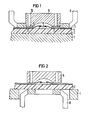
- a printed circuit board 2 is located on a support 1, on which a chip 3 rests in the middle as shown in the figure. 4 denotes a conductor track visible at the interface and 5 the associated solder layer. Terminal lugs 6 lead from the chip 3 to a polyimide carrier 7. A thermode 8 surrounds a hold-down device 9 in which bores 10 are provided. The intended solder connections are designated by 11.
- the isolated micropack 3, 6 and 7 is opened with the tweezers in the form of the hold-down device 9 take, positioned on the slot on the circuit board 2 and placed.
- the frame-shaped thermode 8 is then lowered onto the circuit outside the micropack, so that the heat for the soldering process reaches the connection points via the soldered conductor tracks.
- the micropack is held down until the solder has solidified without tension. Thereafter, thermode 8 and hold-down device 9 are lifted off.
- the structure of the soldering iron is changed such that the hold-down device 9 designed as tweezers and the thermode 8 are arranged on the back of the circuit.
- the hold-down device and thermode are designed to be movable in the Z direction.
- the circuit board 2 is the ceramic carrier for a thick-film or thin-film circuit.
Landscapes
- Engineering & Computer Science (AREA)
- Mechanical Engineering (AREA)
- Electric Connection Of Electric Components To Printed Circuits (AREA)
Applications Claiming Priority (2)
| Application Number | Priority Date | Filing Date | Title |
|---|---|---|---|
| DE2931857 | 1979-08-06 | ||
| DE19792931857 DE2931857A1 (de) | 1979-08-06 | 1979-08-06 | Loetbuegel fuer mikroloetstellen |
Publications (2)
| Publication Number | Publication Date |
|---|---|
| EP0023599A2 true EP0023599A2 (fr) | 1981-02-11 |
| EP0023599A3 EP0023599A3 (fr) | 1981-07-15 |
Family
ID=6077756
Family Applications (1)
| Application Number | Title | Priority Date | Filing Date |
|---|---|---|---|
| EP80103935A Withdrawn EP0023599A3 (fr) | 1979-08-06 | 1980-07-09 | Etrier de soudage pour microsoudures |
Country Status (3)
| Country | Link |
|---|---|
| EP (1) | EP0023599A3 (fr) |
| JP (1) | JPS5629397A (fr) |
| DE (1) | DE2931857A1 (fr) |
Cited By (5)
| Publication number | Priority date | Publication date | Assignee | Title |
|---|---|---|---|---|
| US4835847A (en) * | 1988-04-20 | 1989-06-06 | International Business Machines Corp. | Method and apparatus for mounting a flexible film electronic device carrier on a substrate |
| EP0449156A1 (fr) * | 1990-03-28 | 1991-10-02 | SELENIA INDUSTRIE ELETTRONICHE ASSOCIATE S.p.A. | Appareil à braser et procédé employant du gaz chauffé sur un alliage à braser dans un arrangement de pièces à braser |
| DE4105874C1 (fr) * | 1991-02-25 | 1992-07-30 | Messerschmitt-Boelkow-Blohm Gmbh, 8012 Ottobrunn, De | |
| DE4105875C1 (fr) * | 1991-02-25 | 1992-08-13 | Messerschmitt-Boelkow-Blohm Gmbh, 8012 Ottobrunn, De | |
| DE19942384A1 (de) * | 1999-09-04 | 2001-03-15 | Opel Adam Ag | Lötvorrichtung |
Families Citing this family (2)
| Publication number | Priority date | Publication date | Assignee | Title |
|---|---|---|---|---|
| JPS57210694A (en) * | 1981-06-19 | 1982-12-24 | Hitachi Ltd | Method and device for soldering via resistance reflow |
| DE3531715A1 (de) * | 1985-09-05 | 1987-03-12 | Widmaier Fa Hans | Verfahren bzw. einrichtung zum verloeten oberflaechenmontierbarer bauelemente auf mit leitermustern versehenen schaltungstraegerplatten |
Family Cites Families (9)
| Publication number | Priority date | Publication date | Assignee | Title |
|---|---|---|---|---|
| FR1484521A (fr) * | 1965-06-24 | 1967-06-09 | Texas Instruments Inc | Dispositif de montage de composants dans un circuit électronique |
| US3718800A (en) * | 1968-03-05 | 1973-02-27 | Argus Eng Co | Infrared heating apparatus |
| US3522407A (en) * | 1968-03-05 | 1970-08-04 | Argus Eng Co | Heating method |
| US3710481A (en) * | 1971-03-24 | 1973-01-16 | Burroughs Corp | Terminal alignment and connection device for conductors of a multiconductor cable |
| FR2221225A1 (en) * | 1973-03-16 | 1974-10-11 | Honeywell Bull Soc Ind | Joule effect welding tool for electronic elements - esp. for welding conductor connections to integrated circuitry |
| FR2279505A1 (fr) * | 1974-07-22 | 1976-02-20 | Berco Ste Civile Etude Rech | Panne pour fer a souder, ainsi que les fers a souder pourvus de cette panne |
| US3911569A (en) * | 1974-11-18 | 1975-10-14 | Gen Motors Corp | Method and apparatus for bonding miniature semiconductor pill-type components to a circuit board |
| US3912153A (en) * | 1974-11-18 | 1975-10-14 | Gen Motors Corp | Method and apparatus for bonding semiconductor pill-type components to a circuit board |
| DE2640613C2 (de) * | 1976-09-09 | 1985-03-07 | Siemens AG, 1000 Berlin und 8000 München | Verfahren und Vorrichtung zum Kontaktieren von Schaltungsbausteinen in eine Schichtschaltung |
-
1979
- 1979-08-06 DE DE19792931857 patent/DE2931857A1/de not_active Ceased
-
1980
- 1980-07-09 EP EP80103935A patent/EP0023599A3/fr not_active Withdrawn
- 1980-08-06 JP JP10814680A patent/JPS5629397A/ja active Pending
Cited By (6)
| Publication number | Priority date | Publication date | Assignee | Title |
|---|---|---|---|---|
| US4835847A (en) * | 1988-04-20 | 1989-06-06 | International Business Machines Corp. | Method and apparatus for mounting a flexible film electronic device carrier on a substrate |
| EP0449156A1 (fr) * | 1990-03-28 | 1991-10-02 | SELENIA INDUSTRIE ELETTRONICHE ASSOCIATE S.p.A. | Appareil à braser et procédé employant du gaz chauffé sur un alliage à braser dans un arrangement de pièces à braser |
| DE4105874C1 (fr) * | 1991-02-25 | 1992-07-30 | Messerschmitt-Boelkow-Blohm Gmbh, 8012 Ottobrunn, De | |
| DE4105875C1 (fr) * | 1991-02-25 | 1992-08-13 | Messerschmitt-Boelkow-Blohm Gmbh, 8012 Ottobrunn, De | |
| DE19942384A1 (de) * | 1999-09-04 | 2001-03-15 | Opel Adam Ag | Lötvorrichtung |
| DE19942384C2 (de) * | 1999-09-04 | 2001-12-06 | Opel Adam Ag | Lötvorrichtung |
Also Published As
| Publication number | Publication date |
|---|---|
| JPS5629397A (en) | 1981-03-24 |
| EP0023599A3 (fr) | 1981-07-15 |
| DE2931857A1 (de) | 1981-04-16 |
Similar Documents
| Publication | Publication Date | Title |
|---|---|---|
| DE2852753C3 (de) | Verfahren zum Befestigen von Bauelementen mit flächigen Anschlußkontakten auf einer Leiterplatte und Schablone zur Durchführung des Verfahrens | |
| DE69220653T2 (de) | Halbleiterleistungsmodul | |
| DE1283965B (de) | Hermetisch eingeschlossene Halbleiteranordnung | |
| DE1640467B1 (de) | Verfahren zum kontaktgerechten Aufbringen von mikrominiaturisierten Komponenten auf eine dielektrische Grundplatte | |
| DE69113187T2 (de) | Verfahren zur Herstellung einer elektronische Dünnschichtanordnung. | |
| DE19541334A1 (de) | Schaltungssubstrat mit Verbindungsleitungen und Herstellungsprozeß für dasselbe | |
| DE3781596T2 (de) | Verfahren zum montieren veredelter kontaktflaechen auf einem substrat sowie mit diesen kontaktflaechen versehenes substrat. | |
| DE69514438T2 (de) | Mikrowellenoszillator und Verfahren zu dessen Herstellung | |
| DE10194457B4 (de) | System und Verfahren zum Anbringen elektronischer Komponenten auf flexiblen Substraten | |
| EP0464232A1 (fr) | Connecteur de soudure et procédé de fabrication d'un circuit électrique avec ce connecteur de soudure | |
| DE2319287A1 (de) | Verfahren zum entfernen von ueberschuessigem lot von kontaktfingern auf modulsubstraten | |
| DE2640613C2 (de) | Verfahren und Vorrichtung zum Kontaktieren von Schaltungsbausteinen in eine Schichtschaltung | |
| EP0023599A2 (fr) | Etrier de soudage pour microsoudures | |
| EP0420050A2 (fr) | Procédé de soudage de composants sur une plaque de circuit | |
| DE4424831C2 (de) | Verfahren zur Herstellung einer elektrisch leitenden Verbindung | |
| DE2410849A1 (de) | Verfahren zum aufloeten von miniaturbauelementen | |
| DE3231056A1 (de) | Verfahren zum aufbringen von unbedrahteten bauelementen auf leiterplatten | |
| DE68921116T2 (de) | Verfahren zum Erreichen einer selektiven Adhäsionshemmung und -steuerung in Dickschicht-Leitern. | |
| DE69328211T2 (de) | Einbau von elektronischen Komponenten auf Montageplatten mit Hilfe der Reflow-Technik | |
| DE3319339C2 (fr) | ||
| DE9405654U1 (de) | Vorrichtung zum Verlöten und/oder Aufschmelzen von Lötverbindungen von elektronischen Bauteilen | |
| DE3342279C1 (de) | Lötverfahren und Einrichtung zur Durchführung des Verfahrens | |
| DE2242393C2 (de) | Verfahren zur Herstellung einer mehrschichtigen Schaltungsanordnung aus elektrisch isolierenden Schichten | |
| DE2914621A1 (de) | Verfahren zum loeten von bauelementen in hybridschaltkreise und einrichtung zur durchfuehrung des verfahrens | |
| DE4243356A1 (de) | Bestückungsverfahren für eine Leiterplatte |
Legal Events
| Date | Code | Title | Description |
|---|---|---|---|
| PUAI | Public reference made under article 153(3) epc to a published international application that has entered the european phase |
Free format text: ORIGINAL CODE: 0009012 |
|
| AK | Designated contracting states |
Designated state(s): CH FR IT NL |
|
| PUAL | Search report despatched |
Free format text: ORIGINAL CODE: 0009013 |
|
| AK | Designated contracting states |
Designated state(s): CH FR IT NL |
|
| 17P | Request for examination filed |
Effective date: 19811009 |
|
| STAA | Information on the status of an ep patent application or granted ep patent |
Free format text: STATUS: THE APPLICATION IS DEEMED TO BE WITHDRAWN |
|
| 18D | Application deemed to be withdrawn |
Effective date: 19830309 |
|
| RIN1 | Information on inventor provided before grant (corrected) |
Inventor name: WIRBSER, OSCAR Inventor name: UNGER, GREGOR Inventor name: MEIXNER, KARL |