EP0420050A2 - Procédé de soudage de composants sur une plaque de circuit - Google Patents
Procédé de soudage de composants sur une plaque de circuit Download PDFInfo
- Publication number
- EP0420050A2 EP0420050A2 EP19900118136 EP90118136A EP0420050A2 EP 0420050 A2 EP0420050 A2 EP 0420050A2 EP 19900118136 EP19900118136 EP 19900118136 EP 90118136 A EP90118136 A EP 90118136A EP 0420050 A2 EP0420050 A2 EP 0420050A2
- Authority
- EP
- European Patent Office
- Prior art keywords
- component
- soldering
- electrode
- circuit board
- electrodes
- Prior art date
- Legal status (The legal status is an assumption and is not a legal conclusion. Google has not performed a legal analysis and makes no representation as to the accuracy of the status listed.)
- Granted
Links
Images

Classifications
-
- B—PERFORMING OPERATIONS; TRANSPORTING
- B23—MACHINE TOOLS; METAL-WORKING NOT OTHERWISE PROVIDED FOR
- B23K—SOLDERING OR UNSOLDERING; WELDING; CLADDING OR PLATING BY SOLDERING OR WELDING; CUTTING BY APPLYING HEAT LOCALLY, e.g. FLAME CUTTING; WORKING BY LASER BEAM
- B23K3/00—Tools, devices or special appurtenances for soldering, e.g. brazing, or unsoldering, not specially adapted for particular methods
- B23K3/04—Heating appliances
- B23K3/047—Heating appliances electric
- B23K3/0471—Heating appliances electric using resistance rod or bar, e.g. carbon silica
-
- H—ELECTRICITY
- H05—ELECTRIC TECHNIQUES NOT OTHERWISE PROVIDED FOR
- H05K—PRINTED CIRCUITS; CASINGS OR CONSTRUCTIONAL DETAILS OF ELECTRIC APPARATUS; MANUFACTURE OF ASSEMBLAGES OF ELECTRICAL COMPONENTS
- H05K13/00—Apparatus or processes specially adapted for manufacturing or adjusting assemblages of electric components
- H05K13/04—Mounting of components, e.g. of leadless components
- H05K13/046—Surface mounting
- H05K13/0465—Surface mounting by soldering
-
- H—ELECTRICITY
- H05—ELECTRIC TECHNIQUES NOT OTHERWISE PROVIDED FOR
- H05K—PRINTED CIRCUITS; CASINGS OR CONSTRUCTIONAL DETAILS OF ELECTRIC APPARATUS; MANUFACTURE OF ASSEMBLAGES OF ELECTRICAL COMPONENTS
- H05K3/00—Apparatus or processes for manufacturing printed circuits
- H05K3/30—Assembling printed circuits with electric components, e.g. with resistors
- H05K3/32—Assembling printed circuits with electric components, e.g. with resistors electrically connecting electric components or wires to printed circuits
- H05K3/34—Assembling printed circuits with electric components, e.g. with resistors electrically connecting electric components or wires to printed circuits by soldering
- H05K3/341—Surface mounted components
- H05K3/3421—Leaded components
-
- H—ELECTRICITY
- H05—ELECTRIC TECHNIQUES NOT OTHERWISE PROVIDED FOR
- H05K—PRINTED CIRCUITS; CASINGS OR CONSTRUCTIONAL DETAILS OF ELECTRIC APPARATUS; MANUFACTURE OF ASSEMBLAGES OF ELECTRICAL COMPONENTS
- H05K2201/00—Indexing scheme relating to printed circuits covered by H05K1/00
- H05K2201/10—Details of components or other objects attached to or integrated in a printed circuit board
- H05K2201/10613—Details of electrical connections of non-printed components, e.g. special leads
- H05K2201/10621—Components characterised by their electrical contacts
- H05K2201/10689—Leaded Integrated Circuit [IC] package, e.g. dual-in-line [DIL]
-
- H—ELECTRICITY
- H05—ELECTRIC TECHNIQUES NOT OTHERWISE PROVIDED FOR
- H05K—PRINTED CIRCUITS; CASINGS OR CONSTRUCTIONAL DETAILS OF ELECTRIC APPARATUS; MANUFACTURE OF ASSEMBLAGES OF ELECTRICAL COMPONENTS
- H05K2203/00—Indexing scheme relating to apparatus or processes for manufacturing printed circuits covered by H05K3/00
- H05K2203/01—Tools for processing; Objects used during processing
- H05K2203/0195—Tool for a process not provided for in H05K3/00, e.g. tool for handling objects using suction, for deforming objects, for applying local pressure
-
- H—ELECTRICITY
- H05—ELECTRIC TECHNIQUES NOT OTHERWISE PROVIDED FOR
- H05K—PRINTED CIRCUITS; CASINGS OR CONSTRUCTIONAL DETAILS OF ELECTRIC APPARATUS; MANUFACTURE OF ASSEMBLAGES OF ELECTRICAL COMPONENTS
- H05K2203/00—Indexing scheme relating to apparatus or processes for manufacturing printed circuits covered by H05K3/00
- H05K2203/02—Details related to mechanical or acoustic processing, e.g. drilling, punching, cutting, using ultrasound
- H05K2203/0278—Flat pressure, e.g. for connecting terminals with anisotropic conductive adhesive
-
- H—ELECTRICITY
- H05—ELECTRIC TECHNIQUES NOT OTHERWISE PROVIDED FOR
- H05K—PRINTED CIRCUITS; CASINGS OR CONSTRUCTIONAL DETAILS OF ELECTRIC APPARATUS; MANUFACTURE OF ASSEMBLAGES OF ELECTRICAL COMPONENTS
- H05K2203/00—Indexing scheme relating to apparatus or processes for manufacturing printed circuits covered by H05K3/00
- H05K2203/08—Treatments involving gases
- H05K2203/082—Suction, e.g. for holding solder balls or components
-
- H—ELECTRICITY
- H05—ELECTRIC TECHNIQUES NOT OTHERWISE PROVIDED FOR
- H05K—PRINTED CIRCUITS; CASINGS OR CONSTRUCTIONAL DETAILS OF ELECTRIC APPARATUS; MANUFACTURE OF ASSEMBLAGES OF ELECTRICAL COMPONENTS
- H05K3/00—Apparatus or processes for manufacturing printed circuits
- H05K3/30—Assembling printed circuits with electric components, e.g. with resistors
- H05K3/303—Assembling printed circuits with electric components, e.g. with resistors with surface mounted components
-
- Y—GENERAL TAGGING OF NEW TECHNOLOGICAL DEVELOPMENTS; GENERAL TAGGING OF CROSS-SECTIONAL TECHNOLOGIES SPANNING OVER SEVERAL SECTIONS OF THE IPC; TECHNICAL SUBJECTS COVERED BY FORMER USPC CROSS-REFERENCE ART COLLECTIONS [XRACs] AND DIGESTS
- Y02—TECHNOLOGIES OR APPLICATIONS FOR MITIGATION OR ADAPTATION AGAINST CLIMATE CHANGE
- Y02P—CLIMATE CHANGE MITIGATION TECHNOLOGIES IN THE PRODUCTION OR PROCESSING OF GOODS
- Y02P70/00—Climate change mitigation technologies in the production process for final industrial or consumer products
- Y02P70/50—Manufacturing or production processes characterised by the final manufactured product
Definitions
- the invention relates to a method for soldering components onto printed circuit boards using a soldering device with at least one clip electrode that can be heated by electrical resistance heat.
- Soldering devices with bracket electrodes attached to a soldering iron holder and heatable by electrical resistance heat are known, for example, from DE-A-31 49 236, DE-A-28 18 958 or EP-A-0 011 046.
- soldering devices with two stirrup electrodes lying opposite one another in parallel or with four mutually opposite stirrup electrodes are used in particular for the soldering of multi-pole electronic components such as micropacks, flat packs and the like. If such a soldering device is additionally equipped with a suction pipette arranged centrally between the clip electrodes, this can be used for the automatic assembly of the printed circuit boards with the components to be soldered on.
- the combined assembly and soldering head moves over the feed modules of the components and the circuit board arranged in the assembly area, the suction pipette picking up the respective component from a feed module and depositing it in the specified assembly position on the circuit board.
- the soldering bracket holder is then lowered, so that there is as safe a contact as possible between the working surfaces of the bracket electrodes, the connecting legs of the component and the conductor tracks or connecting pads of the printed circuit board both before the soldering process and during the entire duration of the soldering process .
- the suction pipette can remain on the component until the soldering process has ended and press it against the soldering point on the circuit board with a limited force.
- the solder provided for the soldering melts, which leads to a so-called sagging or sagging of the ironing electrodes.
- the size of the corresponding bag stroke of the ironing electrodes is primarily dependent on the force exerted on the soldering iron holder, although other factors such as e.g. Bent or differently shaped connection pins of the components or how an inclination of the components on the circuit board can exert a not inconsiderable influence.
- the invention has for its object to provide a method for soldering components on printed circuit boards, in which the connection pins of the components with the associated conductor tracks or connection pads of the printed circuit boards are connected to one another by at least largely reproducible soldering of consistently high quality.
- the invention is based on the finding that when the connecting pins are pressed into the molten solder, for example, due to premature seating of one or more connecting pins, differently designed soldering points are created, and that these differences are compensated for by reducing the force exerted on the clip electrode and / or by resetting the clip electrode in a defined manner can. These two measures taken individually or together then cause the formation of defined solder layers between the connection pins and the associated conductor tracks or connection pads.
- the component is placed with a suction pipette in step a) and the component is pressed against the guide plate by exerting a limited force on the suction pipette.
- the component can be withdrawn with the suction pipette against the clip electrode, so that solder layers of the same thickness are guaranteed for all the soldering points of a soldering process.
- the further infeed according to step e) is monitored and limited to a predetermined value.
- the quality of the individual solder joints can be further improved and, in addition, an undesired leakage of the molten solder between the connecting pins and conductor tracks or connecting pads can be prevented.
- the soldering device shown has four U-shaped bracket electrodes attached to a soldering bracket holder LH, two bracket electrodes B1 and two bracket electrodes B2 being aligned parallel to one another in such a way that the working surfaces on the underside of the bracket electrodes B1 and B2 have a rectangular shape which is not closed in the end regions or form a square frame.
- the dimensions of this frame are matched to the shape and position of the connection legs A of a component BE to be soldered onto the connection pads AP of a printed circuit board LP.
- the components BE to be soldered are removed from a magazine or from a feed module with the suction pipette S of a placement head (not shown in the drawing) and placed on the predefined solder joint on the printed circuit board LP.
- the structure and mode of operation of a placement head equipped with a suction pipette can be seen, for example, from US Pat. No. 4,135,630.
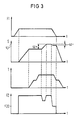
- the suction pipette S can then be used without any problems to limit the precisely positioned component BE before the soldering process up to a time shortly before the end of the soldering process, with one also shown in FIG Force F1 of, for example, 0.1 N to 0.5 N against the circuit board LP.
- the soldering iron contact LH is moved downwards, i. H. the bracket electrodes B1 and B2 are lowered onto the connection legs A of the component BE.
- a force F2 also shown in FIG. 3, of 40 N, for example, the connecting pins A are then pressed via the clip electrodes B1 or B2 to the associated connecting pads AP of the printed circuit board LP.
- FIG. 3 also shows the path or infeed S as a function of time t for the entire duration of a soldering process evident. It can be seen that after the bow electrodes B1 and B2 have been lowered and the solder has started to melt shortly after the maximum temperature has been reached, the connection pins A are pressed into the melted solder. This further pressing is shown by the further infeed sz + of the bracket electrodes B1 and B2.
- the further infeed sz + - which can also be referred to as the bag stroke is monitored by a path measurement system not shown in the drawing and limited to a predetermined, programmable value SP.
- the further infeed is, for example, 20 to 30 micrometers.
- the force F2 exerted on the bracket electrodes B1 and B2 is reduced to a programmed force F20 of, for example, 10 to 15 N.
- a programmed force F20 of, for example, 10 to 15 N.
- F20 a programmed force
- the component BE is then withdrawn with the suction pipette S against the clip electrodes B1 and B2. This last-mentioned measure can, however, be omitted if the connection legs A press against the set-back bracket electrodes B1 and B2 due to their elasticity.
Landscapes
- Engineering & Computer Science (AREA)
- Manufacturing & Machinery (AREA)
- Microelectronics & Electronic Packaging (AREA)
- Mechanical Engineering (AREA)
- Electric Connection Of Electric Components To Printed Circuits (AREA)
- Manufacturing Of Electrical Connectors (AREA)
- Coupling Device And Connection With Printed Circuit (AREA)
Applications Claiming Priority (2)
| Application Number | Priority Date | Filing Date | Title |
|---|---|---|---|
| DE3932702 | 1989-09-29 | ||
| DE3932702 | 1989-09-29 |
Publications (3)
| Publication Number | Publication Date |
|---|---|
| EP0420050A2 true EP0420050A2 (fr) | 1991-04-03 |
| EP0420050A3 EP0420050A3 (en) | 1992-02-05 |
| EP0420050B1 EP0420050B1 (fr) | 1994-12-28 |
Family
ID=6390569
Family Applications (1)
| Application Number | Title | Priority Date | Filing Date |
|---|---|---|---|
| EP90118136A Expired - Lifetime EP0420050B1 (fr) | 1989-09-29 | 1990-09-20 | Procédé de soudage de composants sur une plaque de circuit |
Country Status (5)
| Country | Link |
|---|---|
| US (1) | US5081336A (fr) |
| EP (1) | EP0420050B1 (fr) |
| JP (1) | JP2606807B2 (fr) |
| AT (1) | ATE116513T1 (fr) |
| DE (1) | DE59008127D1 (fr) |
Cited By (4)
| Publication number | Priority date | Publication date | Assignee | Title |
|---|---|---|---|---|
| DE4123987A1 (de) * | 1991-07-19 | 1993-01-21 | Allen Bradley Gmbh | Verfahren und vorrichtung zum elektrisch-leitenden verbinden von an einer leiterplatte angeordneten leiterbahnen im smt-verfahren (surface mount technologie) mit den anschlussdraehten von an der leiterplatte anordbaren bauteilen |
| DE4330467C1 (de) * | 1993-09-08 | 1994-09-08 | Siemens Nixdorf Inf Syst | Verfahren zum Löten von oberflächenmontierbaren elektronischen Bauelementen auf Leiterplatten |
| FR2897503A1 (fr) * | 2006-02-16 | 2007-08-17 | Valeo Sys Controle Moteur Sas | Procede de fabrication d'un module electronique par fixation sequentielle des composants et ligne de production correspondante |
| WO2013087371A1 (fr) * | 2011-12-13 | 2013-06-20 | Robert Bosch Gmbh | Appareil de commande d'un véhicule automobile |
Families Citing this family (10)
| Publication number | Priority date | Publication date | Assignee | Title |
|---|---|---|---|---|
| US6288365B1 (en) * | 1999-05-18 | 2001-09-11 | Mcammond Matthew J. | Soldering assembly |
| DE10042661B4 (de) | 1999-09-10 | 2006-04-13 | Esec Trading S.A. | Verfahren und Vorrichtungen für die Montage von Halbleiterchips |
| US6985780B2 (en) * | 2000-03-10 | 2006-01-10 | Adept Technology, Inc. | Smart camera |
| US6605500B2 (en) * | 2000-03-10 | 2003-08-12 | Infotech Ag | Assembly process |
| ATE423392T1 (de) | 2000-03-10 | 2009-03-15 | Infotech Ag | Verfahren und vorrichtung zum justieren eines bauelementes auf einem substrat unter verwendung von digitaler merkmaltrennung |
| US6988008B2 (en) * | 2000-03-10 | 2006-01-17 | Adept Technology, Inc. | Smart camera |
| EP1424884A1 (fr) * | 2002-11-29 | 2004-06-02 | Leica Geosystems AG | Méthode de montage de composants miniaturisés sur une plaque de support |
| GB2576524B (en) | 2018-08-22 | 2022-08-03 | Pragmatic Printing Ltd | Profiled Thermode |
| CN112139624B (zh) * | 2020-08-17 | 2022-12-06 | 惠州市德泓科技有限公司 | 焊接方法 |
| CN113369630B (zh) * | 2021-05-06 | 2022-10-18 | 渤海造船厂集团有限公司 | 一种基板焊接治具 |
Family Cites Families (14)
| Publication number | Priority date | Publication date | Assignee | Title |
|---|---|---|---|---|
| DE11046C (de) * | C. ZENDER in Berlin S., Brandenburgstrafse 24 | Neuerungen an Hosenträgern | ||
| DE2640613C2 (de) * | 1976-09-09 | 1985-03-07 | Siemens AG, 1000 Berlin und 8000 München | Verfahren und Vorrichtung zum Kontaktieren von Schaltungsbausteinen in eine Schichtschaltung |
| FR2388626A1 (fr) * | 1977-04-29 | 1978-11-24 | Cii Honeywell Bull | Outil de micro soudage perfectionne |
| US4135630A (en) * | 1977-12-08 | 1979-01-23 | Universal Instruments Corporation | Centering device for automatic placement of chip components in hybrid circuits |
| CH639306A5 (fr) * | 1980-12-19 | 1983-11-15 | Far Fab Assortiments Reunies | Outil de soudage. |
| US4552300A (en) * | 1983-05-09 | 1985-11-12 | Pace, Incorporated | Method and apparatus for soldering and desoldering leadless semiconductor modules for printed wiring boards |
| US4605833A (en) * | 1984-03-15 | 1986-08-12 | Westinghouse Electric Corp. | Lead bonding of integrated circuit chips |
| US4805830A (en) * | 1986-04-09 | 1989-02-21 | Apollo Seiko Ltd. | Method for soldering arrayed terminals and an automatic soldering device |
| JPS63174780A (ja) * | 1987-01-12 | 1988-07-19 | Toshiba Corp | 電子部品実装装置 |
| JPS63246892A (ja) * | 1987-04-01 | 1988-10-13 | 三菱電機株式会社 | 半導体搭載装置 |
| DE3722765A1 (de) * | 1987-07-09 | 1989-01-19 | Productech Gmbh | Geheizter stempel |
| JPS6448495A (en) * | 1987-08-19 | 1989-02-22 | Fujitsu Ltd | Soldering device for flat package ic |
| US4982890A (en) * | 1989-01-10 | 1991-01-08 | Siemens Aktiengesellschaft | Soldering means having at least one stirrup electrode and two soldering webs lying opposite one another or four soldering webs lying opposite one another in pairs |
| US4942282A (en) * | 1989-06-16 | 1990-07-17 | Hughes Aircraft Company | Split heater bar |
-
1990
- 1990-09-20 DE DE59008127T patent/DE59008127D1/de not_active Expired - Fee Related
- 1990-09-20 AT AT90118136T patent/ATE116513T1/de not_active IP Right Cessation
- 1990-09-20 EP EP90118136A patent/EP0420050B1/fr not_active Expired - Lifetime
- 1990-09-25 US US07/588,033 patent/US5081336A/en not_active Expired - Fee Related
- 1990-09-27 JP JP2258786A patent/JP2606807B2/ja not_active Expired - Lifetime
Cited By (6)
| Publication number | Priority date | Publication date | Assignee | Title |
|---|---|---|---|---|
| DE4123987A1 (de) * | 1991-07-19 | 1993-01-21 | Allen Bradley Gmbh | Verfahren und vorrichtung zum elektrisch-leitenden verbinden von an einer leiterplatte angeordneten leiterbahnen im smt-verfahren (surface mount technologie) mit den anschlussdraehten von an der leiterplatte anordbaren bauteilen |
| DE4330467C1 (de) * | 1993-09-08 | 1994-09-08 | Siemens Nixdorf Inf Syst | Verfahren zum Löten von oberflächenmontierbaren elektronischen Bauelementen auf Leiterplatten |
| EP0642298A1 (fr) * | 1993-09-08 | 1995-03-08 | Siemens Nixdorf Informationssysteme AG | Méthode de soudage de composants électroniques pour montage à la surface des plaques de circuit |
| FR2897503A1 (fr) * | 2006-02-16 | 2007-08-17 | Valeo Sys Controle Moteur Sas | Procede de fabrication d'un module electronique par fixation sequentielle des composants et ligne de production correspondante |
| WO2013087371A1 (fr) * | 2011-12-13 | 2013-06-20 | Robert Bosch Gmbh | Appareil de commande d'un véhicule automobile |
| US9516750B2 (en) | 2011-12-13 | 2016-12-06 | Robert Bosch Gmbh | Control unit for a motor vehicle |
Also Published As
| Publication number | Publication date |
|---|---|
| EP0420050A3 (en) | 1992-02-05 |
| US5081336A (en) | 1992-01-14 |
| DE59008127D1 (de) | 1995-02-09 |
| JP2606807B2 (ja) | 1997-05-07 |
| ATE116513T1 (de) | 1995-01-15 |
| EP0420050B1 (fr) | 1994-12-28 |
| JPH03124095A (ja) | 1991-05-27 |
Similar Documents
| Publication | Publication Date | Title |
|---|---|---|
| DE2321828C2 (de) | Anschlußklemmenanordnung | |
| DE69223964T2 (de) | Leiterrahmen fuer integrierte oder aehnliche schaltungen | |
| EP0420050B1 (fr) | Procédé de soudage de composants sur une plaque de circuit | |
| DE69022605T2 (de) | Elektrische Verbindungsvorrichtung. | |
| DE3780025T2 (de) | Doppelloetverfahren zur verbindung der anschlusskontakte von elektrischen bauelementen mit den leitern von gedruckten schaltungen. | |
| DE2852753C3 (de) | Verfahren zum Befestigen von Bauelementen mit flächigen Anschlußkontakten auf einer Leiterplatte und Schablone zur Durchführung des Verfahrens | |
| DE69109137T2 (de) | Oberflächenmontage-Verfahren und Vorrichtung. | |
| DE4203605A1 (de) | Elektrischer verbinder | |
| DE2608250A1 (de) | Verfahren zum kontaktieren von auf halbleiterkoerpern befindlichen anschlusskontakten | |
| DE69718755T2 (de) | Verfahren und Vorrichtung zur Herstellung einer elektronischen Schaltungsanordnung mit gleichförmigen Lötrückständen bei Übertragung von Lotpaste | |
| DE102010002150A1 (de) | Lötmaske für Wellenlötverfahren und Verfahren zum Selektivlöten einzelner Bauteile einer Leiterplatte in einem Wellenlöt-Automaten | |
| DE19903957B4 (de) | Verfahren und Vorrichtung zum Entfernen von Lot | |
| DE4330467C1 (de) | Verfahren zum Löten von oberflächenmontierbaren elektronischen Bauelementen auf Leiterplatten | |
| DE7520602U (de) | Elektrisches Gerät mit einem bei unzulässiger Erwärmung selbst auslötenden Widerstand, insbesondere Fernsehempfänger | |
| DE3500411C2 (de) | Verfahren zum Lötverbinden der Leiterbahnen einer flexiblen gedruckten Leitung oder Schaltung mit den Anschlußflächen einer Leiterplatte | |
| EP0419995B1 (fr) | Dispositif de soudage pour souder des composants sur des plaquettes à circuits imprimés | |
| EP0419996B1 (fr) | Dispositif de soudage pour souder des composants sur des plaquettes à circuits imprimés | |
| DE69328211T2 (de) | Einbau von elektronischen Komponenten auf Montageplatten mit Hilfe der Reflow-Technik | |
| DE112019007081T5 (de) | Leiterplatte | |
| DE4310930A1 (de) | Leiterplattenanordnung und Verfahren zur Herstellung einer bestückten Leiterplatte | |
| WO2006013145A1 (fr) | Plaquette a elements smd et au moins un element cable, et procede pour rapporter, fixer et mettre en contact electriquement des elements | |
| DE4204882C2 (de) | Vorrichtung und Verfahren zum Bestücken von oberflächenmontierbaren Bauelementen mit kleinen Kontaktabständen | |
| EP0023599A2 (fr) | Etrier de soudage pour microsoudures | |
| EP0305696B1 (fr) | Procédé de désoudage de composants SMD montés en surface et collés | |
| EP0768815A1 (fr) | Procédé de fabrication de circuits électriques avec un panneau à circuit |
Legal Events
| Date | Code | Title | Description |
|---|---|---|---|
| PUAI | Public reference made under article 153(3) epc to a published international application that has entered the european phase |
Free format text: ORIGINAL CODE: 0009012 |
|
| 17P | Request for examination filed |
Effective date: 19901205 |
|
| AK | Designated contracting states |
Kind code of ref document: A2 Designated state(s): AT BE CH DE FR GB IT LI NL |
|
| RAP1 | Party data changed (applicant data changed or rights of an application transferred) |
Owner name: SIEMENS NIXDORF INFORMATIONSSYSTEME AG |
|
| PUAL | Search report despatched |
Free format text: ORIGINAL CODE: 0009013 |
|
| AK | Designated contracting states |
Kind code of ref document: A3 Designated state(s): AT BE CH DE FR GB IT LI NL |
|
| RAP3 | Party data changed (applicant data changed or rights of an application transferred) |
Owner name: SIEMENS NIXDORF INFORMATIONSSYSTEME AG |
|
| 17Q | First examination report despatched |
Effective date: 19940322 |
|
| GRAA | (expected) grant |
Free format text: ORIGINAL CODE: 0009210 |
|
| AK | Designated contracting states |
Kind code of ref document: B1 Designated state(s): AT BE CH DE FR GB IT LI NL |
|
| REF | Corresponds to: |
Ref document number: 116513 Country of ref document: AT Date of ref document: 19950115 Kind code of ref document: T |
|
| REF | Corresponds to: |
Ref document number: 59008127 Country of ref document: DE Date of ref document: 19950209 |
|
| ITF | It: translation for a ep patent filed | ||
| GBT | Gb: translation of ep patent filed (gb section 77(6)(a)/1977) |
Effective date: 19950303 |
|
| ET | Fr: translation filed | ||
| PLBE | No opposition filed within time limit |
Free format text: ORIGINAL CODE: 0009261 |
|
| STAA | Information on the status of an ep patent application or granted ep patent |
Free format text: STATUS: NO OPPOSITION FILED WITHIN TIME LIMIT |
|
| 26N | No opposition filed | ||
| PGFP | Annual fee paid to national office [announced via postgrant information from national office to epo] |
Ref country code: AT Payment date: 19960904 Year of fee payment: 7 |
|
| PGFP | Annual fee paid to national office [announced via postgrant information from national office to epo] |
Ref country code: BE Payment date: 19960911 Year of fee payment: 7 |
|
| PG25 | Lapsed in a contracting state [announced via postgrant information from national office to epo] |
Ref country code: AT Free format text: LAPSE BECAUSE OF NON-PAYMENT OF DUE FEES Effective date: 19970920 |
|
| PG25 | Lapsed in a contracting state [announced via postgrant information from national office to epo] |
Ref country code: BE Free format text: LAPSE BECAUSE OF NON-PAYMENT OF DUE FEES Effective date: 19970930 |
|
| BERE | Be: lapsed |
Owner name: SIEMENS NIXDORF INFORMATIONSSYSTEME A.G. Effective date: 19970930 |
|
| REG | Reference to a national code |
Ref country code: GB Ref legal event code: IF02 |
|
| PGFP | Annual fee paid to national office [announced via postgrant information from national office to epo] |
Ref country code: NL Payment date: 20030903 Year of fee payment: 14 |
|
| PGFP | Annual fee paid to national office [announced via postgrant information from national office to epo] |
Ref country code: GB Payment date: 20030904 Year of fee payment: 14 |
|
| PGFP | Annual fee paid to national office [announced via postgrant information from national office to epo] |
Ref country code: FR Payment date: 20030930 Year of fee payment: 14 |
|
| PGFP | Annual fee paid to national office [announced via postgrant information from national office to epo] |
Ref country code: DE Payment date: 20031117 Year of fee payment: 14 |
|
| PGFP | Annual fee paid to national office [announced via postgrant information from national office to epo] |
Ref country code: CH Payment date: 20031203 Year of fee payment: 14 |
|
| PG25 | Lapsed in a contracting state [announced via postgrant information from national office to epo] |
Ref country code: GB Free format text: LAPSE BECAUSE OF NON-PAYMENT OF DUE FEES Effective date: 20040920 |
|
| PG25 | Lapsed in a contracting state [announced via postgrant information from national office to epo] |
Ref country code: LI Free format text: LAPSE BECAUSE OF NON-PAYMENT OF DUE FEES Effective date: 20040930 Ref country code: CH Free format text: LAPSE BECAUSE OF NON-PAYMENT OF DUE FEES Effective date: 20040930 |
|
| PG25 | Lapsed in a contracting state [announced via postgrant information from national office to epo] |
Ref country code: NL Free format text: LAPSE BECAUSE OF NON-PAYMENT OF DUE FEES Effective date: 20050401 Ref country code: DE Free format text: LAPSE BECAUSE OF NON-PAYMENT OF DUE FEES Effective date: 20050401 |
|
| GBPC | Gb: european patent ceased through non-payment of renewal fee |
Effective date: 20040920 |
|
| REG | Reference to a national code |
Ref country code: CH Ref legal event code: PL |
|
| PG25 | Lapsed in a contracting state [announced via postgrant information from national office to epo] |
Ref country code: FR Free format text: LAPSE BECAUSE OF NON-PAYMENT OF DUE FEES Effective date: 20050531 |
|
| NLV4 | Nl: lapsed or anulled due to non-payment of the annual fee |
Effective date: 20050401 |
|
| REG | Reference to a national code |
Ref country code: FR Ref legal event code: ST |
|
| PG25 | Lapsed in a contracting state [announced via postgrant information from national office to epo] |
Ref country code: IT Free format text: LAPSE BECAUSE OF NON-PAYMENT OF DUE FEES;WARNING: LAPSES OF ITALIAN PATENTS WITH EFFECTIVE DATE BEFORE 2007 MAY HAVE OCCURRED AT ANY TIME BEFORE 2007. THE CORRECT EFFECTIVE DATE MAY BE DIFFERENT FROM THE ONE RECORDED. Effective date: 20050920 |