EP0025155B1 - Dispositif de mémoire non-volatile à semi-conducteurs - Google Patents
Dispositif de mémoire non-volatile à semi-conducteurs Download PDFInfo
- Publication number
- EP0025155B1 EP0025155B1 EP80105009A EP80105009A EP0025155B1 EP 0025155 B1 EP0025155 B1 EP 0025155B1 EP 80105009 A EP80105009 A EP 80105009A EP 80105009 A EP80105009 A EP 80105009A EP 0025155 B1 EP0025155 B1 EP 0025155B1
- Authority
- EP
- European Patent Office
- Prior art keywords
- mos transistor
- memory cell
- coupled
- control signal
- mos
- Prior art date
- Legal status (The legal status is an assumption and is not a legal conclusion. Google has not performed a legal analysis and makes no representation as to the accuracy of the status listed.)
- Expired
Links
- 239000004065 semiconductor Substances 0.000 title claims description 48
- 230000015654 memory Effects 0.000 claims description 94
- 239000000758 substrate Substances 0.000 claims description 29
- 230000007274 generation of a signal involved in cell-cell signaling Effects 0.000 claims description 12
- 230000009471 action Effects 0.000 claims description 9
- 230000004044 response Effects 0.000 description 12
- 230000003071 parasitic effect Effects 0.000 description 10
- 238000010586 diagram Methods 0.000 description 9
- 230000008878 coupling Effects 0.000 description 7
- 238000010168 coupling process Methods 0.000 description 7
- 238000005859 coupling reaction Methods 0.000 description 7
- 230000002093 peripheral effect Effects 0.000 description 5
- 101150037603 cst-1 gene Proteins 0.000 description 4
- 230000000694 effects Effects 0.000 description 4
- 230000015556 catabolic process Effects 0.000 description 3
- 230000007423 decrease Effects 0.000 description 3
- 230000006870 function Effects 0.000 description 3
- 238000002955 isolation Methods 0.000 description 3
- 239000011159 matrix material Substances 0.000 description 3
- 230000004048 modification Effects 0.000 description 3
- 238000012986 modification Methods 0.000 description 3
- 230000015572 biosynthetic process Effects 0.000 description 2
- 238000010276 construction Methods 0.000 description 2
- 230000005669 field effect Effects 0.000 description 1
- 238000009413 insulation Methods 0.000 description 1
- 230000007246 mechanism Effects 0.000 description 1
- 238000009877 rendering Methods 0.000 description 1
Images




Classifications
-
- G—PHYSICS
- G11—INFORMATION STORAGE
- G11C—STATIC STORES
- G11C16/00—Erasable programmable read-only memories
- G11C16/02—Erasable programmable read-only memories electrically programmable
- G11C16/04—Erasable programmable read-only memories electrically programmable using variable threshold transistors, e.g. FAMOS
- G11C16/0408—Erasable programmable read-only memories electrically programmable using variable threshold transistors, e.g. FAMOS comprising cells containing floating gate transistors
- G11C16/0416—Erasable programmable read-only memories electrically programmable using variable threshold transistors, e.g. FAMOS comprising cells containing floating gate transistors comprising cells containing a single floating gate transistor and no select transistor, e.g. UV EPROM
Definitions
- This invention relates to a nonvolatile semiconductor memory device as defined in the precharacterizing part of the claim 1.
- MOS FET N-channel metal-oxide-semiconductor field effect transistor
- MOS FET N-channel metal-oxide-semiconductor field effect transistor
- bipolar transistor action can be said to have been induced by the lowest drain voltage when the hole current flowing into the substrate is at its maximum.
- bipolar transistor action refer to "Breakdown mechanism in short-channel MOS transistor" by E. Sun et al. on pp. 472-482 of 1978 edition of IEDM.
- a writing operation is executed by injecting the floating gate with electrons produced from the electron-hole pairs by impact ionization.
- the holes produced by the impact ionization flows into the substrate to increase the potential thereat, exerting a bad influence upon transistor circuits forming a decoder and other peripheral components around the memory cell, as well as upon the memory cell itself.
- a writing mode for example, a high voltage is supplied from the decoder circuit to the gate of the MOS FET of the memory cell by means of a gate control line. In this case, as aforesaid, the substrate potential increases, and a current is urged to flow .
- a depletion-type load MOS FET 1 and a driving MOS FET 2 are coupled in series between a power supply terminal Vp and a ground terminal, and a floating-gate type MOS FET 3 forming a memory cell is coupled between a data terminal V D and the ground terminal.
- the gates of the MOS FET's 1 and 3 are both coupled to a junction between the MOS FET's 1 and 2, while the gate of the MOS FET 2 is coupled to a control voltage terminal V CI'
- MOS FET 1 further includes a depletion-type load MOS FET 4 and a driving MOS FET 5 coupled in the same manner as the MOS FET's 1 and 2, and a floating-gate type MOS FET 6 coupled in the same manner as the MOS FET 3.
- the gate of the MOS FET 5, however, is coupled to another control voltage terminal V C2'
- a suitable control voltage is applied to the control voltage terminal V C1 to bring the MOS FET 2 into the nonconducting state.
- a high voltage is applied to the gate of the MOS FET 3 via the MOS FET 1, and data is written in the MOS FET 3 in accordance with the level of a voltage supplied to the data terminal V D .
- the MOS FET 1 is disposed in close vicinity to the MOS FET 3 forming the memory cell in consideration of the pattern layout of various semiconductor elements. Accordingly, when the substrate potential is increased in the data writing mode, a bipolar transistor action will be caused by the source regions of the MOS FET's 1 and 3 and the substrate region between these source regions to cause a current to flow from the source region of the MOS FET 1 to the source region of the MOS FET 3. In consequence, the gate voltage of the MOS FET 3 is lowered, and it becomes hard to write data in the memory cell formed of the MOS FET 3.
- Fig. 2 is a schematic diagram of a semiconductor structure for illustrating the arrangements of the MOS FET's 1, and 6 shown in Fig. 1.
- the MOS FET 1 includes a drain region D1 and a source region S1
- the MOS FET 3 includes a drain region D3 and a source region S3
- the MOS FET 6 includes a drain region D6 and a source region S6.
- a parasitic MOS FET 7 including the semiconductor regions S1 and S3 as its source and drain regions, respectively.
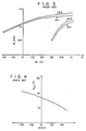
- Fig. 3 shows the relationship between the substrate potential V s and an current Is caused by the bipolar transistor action to flow into the parasitic MOS FET 7 including the semiconductor regions S1 and S3 in the semiconductor structure shown in Fig. 2.
- solid lines SL1 and SL2 are characteristic curves representing cases where the gate voltage is set to 25V and the drain voltage is set to 5V and 25V, respectively, while broken lines BL1 and BL2 are characteristic curves representing cases where the gate voltage is set to 0V and the drain voltage is set to 5V and 25V respectively.
- Fig. 4 shows the relationship between the threshold voltage V TH and substrate voltage V s of the parasitic MOS FET 7.
- the parasitic MOS FET 7 which has a threshold voltage of approximately 17V in the normal state orwhen the substrate voltage V s is 0V, will have a substantially reduced threshold voltage of 11V when the substrate voltage V s becomes 0.4V, for example.
- peripheral circuits will be greatly influenced by the variations of the substrate voltage V s .
- Figs. 5 to 7 are schematic structural diagrams of the MOS FET for illustrating the impossibility of writing due to a potential drop of a data line in writing data into a memory cell formed of an MOS FET with a floating gate.
- Fig. 5 is a plan view of the MOS FET
- Fig. 6 is a sectional view of the semiconductor structure as taken along line VI-VI of Fig. 5
- Fig. 7 is a sectional view of the semiconductor structure as taken along line VII-VII of Fig. 5.
- the MOS FET includes a source region SR and a drain region DR formed in the surface region of a substrate SB, an isolation layer IL stretching over these two regions SR and DR, a floating gate FG formed within the isolation layer IL, a control gate CG formed over the floating gate FG, and a word line WL formed as a unit with the control gate CG.
- parasitic capacitances formed between the floating gate FG and respective one of the control gate CG, channel region, source region SR, drain region DR and substrate surface are C1, C2, C3, C4 and C5, respectively.
- V F at the floating gate FG may be given by
- the thickness of the insulation layer conducive to the formation of the parasitic capacitances C1 to C4, i.e. the distance between the floating gate FG and the channel region of the substrate SB in Fig. 7, is 1,000 A
- the thickness of the isolation layer conducive to the formation of the parasitic capacitance C5, i.e. the distance between the floating gate FG and the field region of the substrate SB as clearly shown in Fig. 7, is 7,000 A.
- the width of the floating gate FG is three times as large as the channel width
- the length of the floating gate FG is 4 p
- the distances of extension of the drain and source regions DR and SR into a region right under the floating gate FG is 1 p.
- equation (1) may be rewritten as follows:
- V D 20V
- V F 1.16V.
- the threshold voltage of the MOS FET need be set to 1.16V or above. If the threshold voltage is raised, however, the current flowing into the memory cell is reduced in reading out data from the memory cell, so that charging and discharge of the data line require a long time, lowering the reading speed. Conventionally, therefore, the threshold voltage is lowered to such a degree that a leakage current within a negligible range may flow also into a nonselected memory cell in the writing operation.
- MOS FET's are formed so as to have short channel length, thereby causing a short-channel effect. Namely, when a high voltage is applied to the drains of MOS FET's of memory cells arranged on the same column with the selected memory in the writing operation, a current is inevitably caused to flow between the drains and sources of these MOS FET's by a punch-through phenomenon. As a result, the drain voltage is lowered to prevent secure execution of the writing operation.
- the object of this invention is to provide a nonvolatile semiconductor memory device capable of high-reliability operation.
- a nonvolatile semiconductor memory device which comprises at least one memory cell including a first MOS transistor with a floating gate, at least one word line coupled to the gate of said first MOS transistor of said at least one memory cell to selectively transmit an access signal to said at least one memory cell, and at least one data line coupled to the drain of said first MOS transistor of said at least one memory cell to transmit data to be transferred to and from said at least one memory cell, and which is characterized by further comprising potential level control means coupled to the source of said first MOS transistor of said at least one memory cell and maintaining the source potential of said first MOS transistor substantially at a given level which is such as to avoid bipolar transistor action due to a rise in the substrate potential during a writing operation or to suppress the punch through in the memory cell which is not selected.
- Fig. 8 shows a nonvolatile semiconductor memory device according to an embodiment of this invention.
- the memory device comprises a plurality of memory cells MC-11 to MC-MN arranged in the form of a matrix, each of the memory cells being formed of an MOS transistor with a floating gate, word lines W1 to WM each coupled in common with the control gates of the MOS transistors forming memory cells on the same row, data lines D1 to DN each coupled in common with the drains of MOS transistors forming memory cells on the same column, and a resistor R1 coupled in common with the sources of the MOS transistors forming the memory cells MC-11 to MC-MN.
- the memory device is provided with a row selection circuit 10 selecting the word lines W1 to WM in response to an address signal from an address signal generation circuit (not shown), and a column selection circuit 12 selecting one of the data lines D1 to DN in response to the address signal and enabling data to be transferred between a selected memory cell and an external circuit (not shown).
- the word line W1 is selected by an address designation signal from the row selection circuit 10
- the column line D1 is selected by an address designation signal from the column selection circuit 12.
- a writing current flows between the drain and source of the MOS transistor forming the memory cell MC-11. Electrons, for example, out of electron-hole pairs produced by the writing current are trapped by the floating gate of the MOS transistor, and data is written in the memory cell MC-11. Meanwhile, since the writing current slows via the resistor R1, the source potential of the MOS transistor rises.
- the substrate potential of the MOS transistor also rises, the aforementioned bipolar transistor action or punch-through phenomenon due to a substrate potential rise will never be caused if the resistance value of the resistor R1 is so set that a source potential build-up rate higher than the substrate potential build-up rate may be obtained. Furthermore, the source potential is kept higher than the substrate potential, so that the data writing in the memory cell MC-11 may securely be executed without causing any currents to flow from peripheral circuits into the source of the MOS transistor forming the memory cell MC-11, and hence without lowering the potential of the word line W1. Moreover, the existence of the resistor R1 forces the source of the MOS transistor forming the memory cell into which the data is written to be maintained at a higher potential than the substrate.
- peripheral circuits including the row and column selection circuits 10 and 12 can be arranged in close vicinity to the matrix array of memory cells MC-11 to MC-MN to reduce the chip size without causing the matrix array to exert any substantial electrical influences on the peripheral circuits such as row and column selection circuit 10 and 12. Since the source potential is set higher than the substrate potential, moreover, the punch-through phenomenon can be checked satisfactorily. In consequence, the channel length of the memory cell MOS FET can be reduced, so that the memory cells can be arranged with high density.
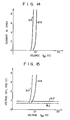
- the threshold voltage VTH of the MOS FET forming the selected memory cell increases as electrons are injected into the floating gate of the MOS FET, that is, with the passage of the writing time.
- the relationship between the threshold voltage V TH and the writing time is shown in Fig. 9.
- solid lines SL3 and LS4 are characteristic curves obtained when the resistance of the resistor R1 is set at great and . small values, respectively.
- the threshold voltage V TH takes a small value at the initial stage of the writing, though it suddenly comes to take a large value after the writing time has passed 1 ms or thereabout.
- the resistor R1 has a small resistance value and is so set as to provide a voltage drop of 0.4V and 0.5V thereacross, the threshold voltage takes a greater value as compared with the foregoing case at the initial stage of writing, though it comes to take a smaller value than the value in the aforesaid case after the writing time has passed 2 ms or thereabout.
- Fig. 10 shows a semiconductor memory circuit constructed in consideration of the relationship between the threshold voltage V TH and the writing time.
- This semiconductor memory circuit is substantially the same as the one shown in Fig. 8, except that it further includes a series circuit including a resistor R2 and an MOS FET 14 are coupled in parallel with the resistor R1 and a pulse generator 16 to control the conduction state of the MOS FET 14 in response to a write enable signal.
- the pulse generator 16 applies a control signal of e.g. high level to the gate of the MOS FET 14.
- a control signal of e.g. high level to the gate of the MOS FET 14.
- the value of resistance existing between the sources of the MOS FET's forming the memory cells MC-11 to MC-MN and the ground is reduced, and the source potentials of these MOS FET's are set between 0.4V and 0.5V, for example. Namely, in this case, the threshold voltage of the MOS FET forming the selected memory cell increases with the passage of the writing time along the curve SL4 of Fig. 9.
- a low-level control signal is produced from the pulse generator 16 to turn off the MOS FET 14.
- the source potentials of the MOS FET's forming the memory cells MC-11 to MC-MN are set between 0.7V and 1.0V, for example. Namely, the threshold voltage of the MOS FET forming the selected memory cell increases with the passage of the writing time at a rate corresponding to the inclination of the curve SL3 of Fig. 9.
- a high-efficiency writing operation can be achieved by changing the resistance of the resistor coupled with the sources of the MOS FET's forming the memory cells from a small value to a great value during the period for such writing operation.
- Fig. 11 shows a semiconductor memory circuit according to another embodiment of this invention having a source potential control circuit 20 which is constructed so as to provide substantially the same effect as the circuit of Fig. 10.
- the source potential control circuit 20 comprises comparators 21 and 22 whose first input terminals are coupled to the sources of the MOS FET's forming the memory cells MC-11 to MC-MN, MOS transistors 24, 25 and 26 whose current paths are coupled between the sources of the MOS FET's and the ground, MOS transistors 28 and 30 having current paths coupled respectively between the comparators 21 and 22 and the ground, and a pulse generator 32 supplying a low-level signal to the gate of the MOS transistor 28 in response to a write enable signal from an external control circuit (not shown) for a given time after the start of the writing operation and supplying the low-level signal to the gate of the MOS transistor 30 for the remaining writing time.
- the comparator 21 receives a reference voltage VR1 of e.g. 0.5V at its second input terminal, and has an output terminal coupled to the gate of the MOS transistor 24.
- the comparator 22 receives a reference voltage VR2 of e.g. 0.9 V at its second input terminal, and has an output terminal coupled to the gate of the MOS transistor 25.
- the MOS transistor 26 is caused to conduct in response to a read enable signal from the external control circuit during a period for reading operation, and is kept in the nonconductive state during the writing operation period.
- the source potential of the MOS FET forming the selected memory cell increases to reach 0.5 V or higher in the writing operation of the semiconductor memory circuit shown in Fig. 11, a high-level signal is produced from the comparator 21. Since the MOS transistor 28 is kept nonconductive by the low-level signal from the pulse generator 32, the high-level signal from the comparator 21 is applied to the gate of the MOS transistor 24, thereby rendering the MOS transistor 24 conductive. Consequently, the source potential of the selected MOS FET is lowered through the MOS transistor 24. When the source potential falls below 0.5 V, an output signal from the comparator 21 is reduced to low level to turn off the MOS transistor 24. Thus, the source potential of the selected MOS FET is to be kept at approximately 0.5 V during the initial writing period.
- the MOS transistor 28 When the initial writing period has passed, the MOS transistor 28 is turned on by control signals from the pulse generator 32, the MOS transistor 24 is set and maintained in the nonconductive state, and the MOS transistor 30 is rendered nonconductive.
- the comparator 22 operates in the same manner as the comparator 21, thereby keeping the source potential of the selected MOS FET at approximately 0.9 V.
- the source potential of the MOS FET forming the selected memory cell is kept at approximately 0.5 V during the initial writing period, and at approximately 0.9 V during the subsequent writing period in the same write-in operation, so that the same effect as described in connection with Fig. 10 may be obtained with use of this semiconductor memory circuit.
- Fig. 12 shows a source potential control circuit 40 having the same function with the source control circuit 20 shown in Fig. 11.
- the control circuit 40 comprises inverters 43 and 44 respectively including MOS transistors 41 and 42 having threshold voltages of e.g. 0.1V and 0.5V, respectively, and whose gates are coupled to a source coupling terminal SCT, inverters 45 and 46 whose input terminals are coupled respectively to the inverters 43 and 44, MOS transistors 47 and 48 coupled between the respective output terminals of the inverters 45 and 46 and the ground, and MOS transistors 49, 50 and 51 whose current paths are coupled between the source coupling terminal SCT and the ground.
- MOS transistors 41 and 42 having threshold voltages of e.g. 0.1V and 0.5V, respectively, and whose gates are coupled to a source coupling terminal SCT
- inverters 45 and 46 whose input terminals are coupled respectively to the inverters 43 and 44
- MOS transistors 47 and 48 coupled between the respective output terminals of the inverters 45 and
- the gates of the MOS transistors 49 and 50 are coupled respectively to the output terminals of the inverters 45 and 46, and the gates of the MOS transistors 47 and 48 are coupled to first and second output terminals of a pulse generator 52 which produces control signals in response to a write enable signal from an external control circuit (not shown). Further the MOS transistors 51 is caused to conduct in response to a read enable signal from the external control circuit in the read-out operation, and is kept in the nonconductive state in the write-in operation.
- the MOS transistor 41 When the source potential of the MOS FET forming the selected memory cell increases to reach approximately 0.5 V in the writing operation mode, the MOS transistor 41 is turned on to cause an output voltage from the inverter 43 to decrease. As a result, an output signal from the inverter 45 increases. In this case, since a low-level signal is supplied from the pulse generator 52 to the gate of the MOS transistor 47, the MOS transistor 47 is kept in the nonconductive state. Accordingly, the MOS transistor 49 is rendered conductive by the high-level signal from the inverter 45, thereby lowering the potential at the source coupling terminal SCT. When the potential at the source coupling terminal SCT is lowered to some degree, the resistance of the MOS transistor 41 becomes large, causing the output voltage of the inverter 43 to increase.
- the output voltage of the inverter 45 decreases, causing the resistance of the MOS transistor 49 to become high and the potential at the source coupling terminal SCT to rise again. That is, in the initial writing period, the potential at the source coupling terminal SCT is maintained at about 0.5 V. After the elapse of the initial writing time, the MOS transistor 47 is rendered conductive in response to a control signal from the pulse generator 52 and the MOS transistor 48 is rendered nonconductive. In the remaining time of the writing period, the inverters 44 and 46 and the MOS transistor 50 function in the same manner as the inverters 43 and 45 and the MOS transistor 49, respectively to maintain the source coupling terminal SCT at about 0.9 V.
- control circuit 40 shown in Fig. 12 operates to maintain at about 0.5 V the source potential of MOS FET forming a memory cell selected in the initial writing period and maintain the same at about 0.9 V after the elapse of the initial writing time. That is, the control circuit 40 functions to provide substantially the same effect as the control circuit 20 shown in Fig. 11.
- FIG. 13 shows a semiconductor memory circuit according to a further embodiment of this invention.
- a column selection circuit 12 in this semiconductor memory circuit includes MOS transistors CST-1 to CST-N whose current paths are coupled respectively to data lines D1 to DN, a load MOS transistor LT having a current path coupled between the MOS transistors CST-1 to CST-N and a power supply terminal V A and controlled for conduction state in accordance with write-in data, e.g. so designed as to be turned on in response to data "1", and a column decoder CD to render one of the MOS transistors CST-1 to CST-N conductive in response to an address signal from an external control circuit (not shown).
- a source potential control circuit 60 is coupled to the sources of the MOS FET's forming memory cells MC-11 to MC-MN.
- the control circuit 60 includes a depletion-type MOS transistor 61, an MOS transistor 62 with a threshold voltage of approximately 0 V, and an MOS transistor 63, the current paths of all these transistors being coupled in series between a power supply terminal V B and the ground.
- a junction between the MOS transistors 61 and 62 is coupled to the gates of the MOS transistors 61 and 63, and a junction between the MOS transistors 62 and 63 is coupled to the sources of the MOS FET's forming the memory cells.
- control circuit 60 includes MOS transistors 64, 65 and 66 whose current paths are coupled in series between the power supply terminal V A and the gate of the transistor 62.
- the MOS transistor 64 is constructed in the same manner as the load transistor LT the MOS transistor 65 as each of the MOS transistors CST-1 to CST-N and the MOS transistor 66 as the MOS FET forming each of the memory cells MC-11 to MC-MN.
- the gates of the MOS transistors 64 and 65 are coupled with a control signal terminal V cs to receive control signals in the writing operation mode, while the gate of the MOS transistor 66 is supplied with a voltage at the same level as the potential of nonselected word lines in the writing operation mode. Namely, a voltage V A is applied to the drain of the MOS transistor 66 through the MOS transistors 64 and 65 in the writing operation, and the source potential of the MOS transistor 66 is maintained at a given level by the punch-through phenomenon, etc.
- the data lines D1 to DN are kept at low-level potential, -so that the source potentoal V s p of the MOS FET's forming the memory cells is low, and the MOS transistors 62 and 63 are maintained slightly conductive, and the source potential V s p is settled at a given level.
- the MOS transistor 62 When the source potential V s p falls below the gate voltage of the MOS transistor 62, the MOS transistor 62 is rendered conductive, thereby reducing the gate voltage of the MOS transistor 63 and increasing the conduction resistance of the MOS transistor 63. In consequence, the source potential V s p increases again. Such an operation is instantaneously effected and the source potential V s p is to be maintained at a constant level corresponding to the source potential of the MOS transistor 66.
- Fig. 14 shows the relationship between the source potential V s p of the MOS FET's forming the memory cells MC-11 to MC-MN and a current Is flowing from these memory cells MC-11 to MC-MN into the MOS transistor 63 in the writing operation mode.
- the source potential V SP varies only about 0.06 V when the current I S varies from 1 mA to 10 mA.
- the source potential of MOS FET's forming memory cells used in a memory for storing e.g. 4-bit data can be kept at a substantially constant level by using the control circuit 60 with the memory.
- Fig. 15 shows the relationship between the source potential V s p and the gate voltages V G1 and V G2 of the MOS transistor 62 and 63.
- the gate voltage V G1 of the MOS transistor 62 is kept substantially constant irrespective of the variation of the source potential V SP , whereas the gate voltage V G2 of the MOS transistor 63 increases drastically when the source potential V s p rises above approximately 0.8 V to 1.0 V.
- the source potential V SP can be maintained between 0.8 V and 1.0 V.
- Figs. 16 and 17 both show modified examples of the source potential control circuit 60 shown in Fig. 13.
- the control circuit shown in Fig. 16 includes a depletion-type MOS transistor 71, an MOS transistor 72 with a low threshold voltage, and an MOS transistor 73 with a higher threshold voltage than. that of the MOS transistor 72 connected in series between the power supply terminal V B and the ground.
- a junction between the MOS transistor 71 and 72 is coupled to the gates of the MOS transistors 71 to 73, and a junction between the MOS transistors 72 and 73 is coupled to a source potential terminal T s p which is coupled to the sources of the MOS FET's forming the memory cells MC-11 to MC-MN.
- a given voltage is applied to the gates of the MOS transistors 72 and 73 via the MOS transistor 71, and the MOS transistors 72 and 73 are maintained in the slightly conductive state.
- the MOS transistor 72 is turned off. Accordingly, the gate voltage of the MOS transistor 73 drastically increases to reduce the conduction resistance of the MOS transistor 73 by a great margin. As a result, the potential at the source potential terminal T SP is lowered and maintained at a given level.
- the control circuit shown in Fig. 17 includes a depletion-type MOS transistor 81 and MOS transistors 82, 83 and 84 coupled in series between the power supply terminal V B and the ground.
- a junction between the MOS transistors 81 and 82 is coupled to the gates of the MOS transistors 81, 82 and 84, a junction between the MOS transistors 82 and 83 is coupled to the gate of the MOS transistor 83, and a junction betweem the MOS transistors 83 and 84 is coupled to the source potential terminal T s p.
- the control circuit of Fig. 17 operates in the same manner as the circuit shown in Fig. 16. Namely, when the potential at the source potential terminal T SP increases, the MOS transistor 82 is turned off so that the gate voltage of the MOS transistor 84 drastically increases to reduce the conduction resistance of the MOS transistor 84, thereby lowering the potential at the source potential terminal T SP .
- Fig. 18 shows still another modified example of the control circuit shown in Fig. 13.
- This control circuit includes a depletion-type MOS transistor 91 and MOS transistors 92 and 93 having current paths coupled in series between the power supply terminal V B and the ground, a depletion-type MOS transistor 94 and an MOS transistor 95 having current paths coupled in series between the power supply terminal V B and the MOS transistor 93, and an MOS transistor 96 having a current path coupled between the source potential terminal T s p and the ground.
- the gate of the MOS transistor 95 is coupled to a junction between the MOS transistors 91 and 92, and the gates of the MOS transistors 92 and 96 are coupled to a junction between the MOS transistors 94 and 95.
- control circuit of Fig. 18 includes depletion-type MOS transistors 97, 98 and 99 and an MOS transistor 100 having current paths coupled in series between the power supply terminal V B and the ground and depletion-type MOS transistors 101 and 102 having current paths coupled in series between the power supply terminal V B and the MOS transistor 99.
- a junction between the MOS transistors 97 and 98 is coupled to the gates of the MOS transistors 94 and 97, and a junction between the MOS transistors 101 and 102 is coupled to the gates of the MOS transistors 91 and 101.
- the gate of the MOS transistor 102 is coupled to the source potential terminal T s p
- a junction between the MOS transistors 99 and 100 is coupled to the gate of the MOS transistor 99
- the gate of the MOS transistor 100 is supplied with a write enable signal.
- the control circuit includes MOS transistors 103 and 104, an MOS FET 105 with the same construction as the MOS FET's forming the memory cells MC-11 to MC-MN, and a depletion-type MOS transistor 106 having current paths coupled in series between the power supply terminal V A and the ground.
- MOS FET 105 A junction between MOS FET 105 and the MOS transistor 106 is coupled to the gate of the MOS transistor 98, the gates of the MOS transistors 103 and 104 are coupled to the control signal terminal V cs , and the gate of the MOS transistor 106 is grounded.
- the MOS transistors 103 and 104 are constructed in the same manner as the MOS transistors LT and CST shown in Fig. 13, respectively, while the MOS FET 105 has the same construction as the MOS FET's forming the memory cells MC-11 to MC-MN.
- a control signal is applied to the control signal terminal V cs , a voltage V A is applied to the drain of the MOS transistor 105 through the MOS transistors 103 and 104, a voltage at the same level as the potential of nonselected word lines is applied to the gate of the MOS transistor 105, and the source potential V sc of the MOS transistor 105 is kept at a constant level.
- the MOS transistors 93 and 100 are both rendered conductive in response to the write enable signal.
- the conduction resistance of the MOS transistor 102 is greater than that of the MOS transistor 98, so that the gate voltage of the MOS transistor 91 is higher than that of the MOS transistor 94. Accordingly, the conduction resistance of the MOS transistor 91 is smaller than that of the MOS transistor 94, so that a gate voltage higher than those of the MOS transistors 92 and 96 is applied to the gate of the MOS transistor 95. As a result, the MOS transistor 96 obtains a great conduction resistance, and the potential at the source potential terminal T s p increases gradually.
- the source potential V s p becomes higher than the source potential V sc , a high voltage is applied to the gate of the MOS transistor 96 to reduce the conduction resistance of the MOS transistor 96, thereby lowering the potential at the source potential terminal T s p.
- the source potential V s p of the MOS FET's forming the memory cells is set to a potential level substantially equal to that of the source potential V sc of the MOS transistor 105.
- the N-channel MOS transistors used in the above-mentioned embodiments can be replaced by P-channel MOS transistors.
- the resistors R1 and R2 used in the embodiments shown in Figs. 8 and 10 may be formed of MOS transistors.
- the MOS transistors 64 to 66 and 103 to 106 can be omitted so that a gate control voltage at a given level may be applied directly to the gates of the MOS transistors 62 and 98.
Landscapes
- Engineering & Computer Science (AREA)
- Microelectronics & Electronic Packaging (AREA)
- Read Only Memory (AREA)
- Semiconductor Memories (AREA)
- Non-Volatile Memory (AREA)
Claims (13)
Applications Claiming Priority (2)
| Application Number | Priority Date | Filing Date | Title |
|---|---|---|---|
| JP54110057A JPS6014438B2 (ja) | 1979-08-29 | 1979-08-29 | 不揮発性半導体メモリ− |
| JP110057/79 | 1979-08-29 |
Publications (3)
| Publication Number | Publication Date |
|---|---|
| EP0025155A2 EP0025155A2 (fr) | 1981-03-18 |
| EP0025155A3 EP0025155A3 (en) | 1982-12-29 |
| EP0025155B1 true EP0025155B1 (fr) | 1985-04-17 |
Family
ID=14525986
Family Applications (1)
| Application Number | Title | Priority Date | Filing Date |
|---|---|---|---|
| EP80105009A Expired EP0025155B1 (fr) | 1979-08-29 | 1980-08-22 | Dispositif de mémoire non-volatile à semi-conducteurs |
Country Status (4)
| Country | Link |
|---|---|
| US (1) | US4425632A (fr) |
| EP (1) | EP0025155B1 (fr) |
| JP (1) | JPS6014438B2 (fr) |
| DE (1) | DE3070511D1 (fr) |
Families Citing this family (24)
| Publication number | Priority date | Publication date | Assignee | Title |
|---|---|---|---|---|
| JPS5654693A (en) * | 1979-10-05 | 1981-05-14 | Hitachi Ltd | Programable rom |
| JPS57192067A (en) * | 1981-05-22 | 1982-11-26 | Hitachi Ltd | Erasable and programmable read only memory unit |
| JPS6074577A (ja) * | 1983-09-30 | 1985-04-26 | Toshiba Corp | 不揮発性半導体メモリ装置 |
| NL8304256A (nl) * | 1983-12-09 | 1985-07-01 | Philips Nv | Halfgeleiderinrichting. |
| US4709352A (en) * | 1984-11-19 | 1987-11-24 | Oki Electric Industry Co., Ltd. | MOS read-only memory systems |
| JPS62130715U (fr) * | 1986-02-04 | 1987-08-18 | ||
| DE3774369D1 (de) * | 1986-08-22 | 1991-12-12 | Fujitsu Ltd | Halbleiter-speicheranordnung. |
| JP2633252B2 (ja) * | 1987-06-11 | 1997-07-23 | 沖電気工業株式会社 | 半導体記憶装置 |
| US6034899A (en) * | 1987-06-29 | 2000-03-07 | Kabushiki Kaisha Toshiba | Memory cell of nonvolatile semiconductor memory device |
| US6545913B2 (en) | 1987-06-29 | 2003-04-08 | Kabushiki Kaisha Toshiba | Memory cell of nonvolatile semiconductor memory device |
| US5877981A (en) * | 1987-06-29 | 1999-03-02 | Kabushiki Kaisha Toshiba | Nonvolatile semiconductor memory device having a matrix of memory cells |
| US5448517A (en) | 1987-06-29 | 1995-09-05 | Kabushiki Kaisha Toshiba | Electrically programmable nonvolatile semiconductor memory device with NAND cell structure |
| JPH0766675B2 (ja) * | 1987-07-14 | 1995-07-19 | 株式会社東芝 | プログラマブルrom |
| JPH0642551B2 (ja) * | 1987-11-12 | 1994-06-01 | 株式会社東芝 | 不揮発性半導体メモリ |
| JP2617189B2 (ja) * | 1987-08-03 | 1997-06-04 | 沖電気工業株式会社 | 電流検出回路 |
| JPH01108778A (ja) * | 1987-10-21 | 1989-04-26 | Mitsubishi Electric Corp | 半導体記憶装置 |
| JP2573335B2 (ja) * | 1988-11-09 | 1997-01-22 | 株式会社東芝 | 不揮発性メモリ |
| US5341329A (en) * | 1988-12-28 | 1994-08-23 | Kabushiki Kaisha Toshiba | Nonvolatile semiconductor memory device capable of preventing read error caused by overerase state and method therefor |
| US5065364A (en) * | 1989-09-15 | 1991-11-12 | Intel Corporation | Apparatus for providing block erasing in a flash EPROM |
| US5313432A (en) * | 1990-05-23 | 1994-05-17 | Texas Instruments Incorporated | Segmented, multiple-decoder memory array and method for programming a memory array |
| US5481494A (en) * | 1994-12-22 | 1996-01-02 | Advanced Micro Devices, Inc. | Method for tightening VT distribution of 5 volt-only flash EEPROMS |
| JPH1145588A (ja) * | 1997-07-25 | 1999-02-16 | Nec Corp | 不揮発性半導体記憶装置 |
| EP0978845A1 (fr) * | 1998-08-07 | 2000-02-09 | STMicroelectronics S.r.l. | Mémoire non-volatile à semi-conducteur, électriquement programmable |
| US20040032319A1 (en) * | 2002-08-17 | 2004-02-19 | Kye-Hyun Kyung | Devices and methods for controlling active termination resistors in a memory system |
Family Cites Families (5)
| Publication number | Priority date | Publication date | Assignee | Title |
|---|---|---|---|---|
| CA813537A (en) | 1967-10-17 | 1969-05-20 | Radio Corporation Of America | Semiconductor memory device |
| US3836894A (en) | 1974-01-22 | 1974-09-17 | Westinghouse Electric Corp | Mnos/sos random access memory |
| DE2514582C2 (de) | 1975-04-03 | 1977-05-26 | Siemens Ag | Schaltung zur erzeugung von leseimpulsen |
| DE2623219B2 (de) * | 1976-05-24 | 1978-10-12 | Siemens Ag, 1000 Berlin Und 8000 Muenchen | Verfahren zum Betreiben einer Leseverstärkerschaltung für einen dynamischen MOS-Speicher und Anordnung zur Durchführung dieses Verfahrens |
| US4301518A (en) | 1979-11-01 | 1981-11-17 | Texas Instruments Incorporated | Differential sensing of single ended memory array |
-
1979
- 1979-08-29 JP JP54110057A patent/JPS6014438B2/ja not_active Expired
-
1980
- 1980-08-22 DE DE8080105009T patent/DE3070511D1/de not_active Expired
- 1980-08-22 EP EP80105009A patent/EP0025155B1/fr not_active Expired
- 1980-08-25 US US06/180,991 patent/US4425632A/en not_active Expired - Lifetime
Also Published As
| Publication number | Publication date |
|---|---|
| US4425632A (en) | 1984-01-10 |
| JPS5634190A (en) | 1981-04-06 |
| JPS6014438B2 (ja) | 1985-04-13 |
| EP0025155A3 (en) | 1982-12-29 |
| EP0025155A2 (fr) | 1981-03-18 |
| DE3070511D1 (en) | 1985-05-23 |
Similar Documents
| Publication | Publication Date | Title |
|---|---|---|
| EP0025155B1 (fr) | Dispositif de mémoire non-volatile à semi-conducteurs | |
| KR910007434B1 (ko) | 전기적으로 소거 및 프로그램 가능한 반도체 메모리장치 및 그 소거 및 프로그램 방법 | |
| US6141250A (en) | Non-volatile semiconductor memory device | |
| US6380636B1 (en) | Nonvolatile semiconductor memory device having an array structure suitable to high-density integrationization | |
| KR100559716B1 (ko) | 낸드 플래시 메모리 소자 및 이의 독출 방법 | |
| KR960001322B1 (ko) | 반도체 메모리 장치 및 이 장치를 위한 데이타 소거 방법 | |
| KR950011295B1 (ko) | 불휘발성 반도체기억장치와 리드온리 메모리 및 그 임계치전압 측정방법 | |
| US5313432A (en) | Segmented, multiple-decoder memory array and method for programming a memory array | |
| US6650566B2 (en) | Nonvolatile semiconductor memory with a programming operation and the method thereof | |
| US5973962A (en) | Method of programming non-volatile memory devices having a NAND type cell array | |
| US4999812A (en) | Architecture for a flash erase EEPROM memory | |
| US5790456A (en) | Multiple bits-per-cell flash EEPROM memory cells with wide program and erase Vt window | |
| KR970004072B1 (ko) | 플로팅 게이트를 갖는 불휘발성 반도체 기억장치 | |
| KR100374522B1 (ko) | 메모리 어레이의 면적을 축소할 수 있는 비휘발성 반도체기억 장치 | |
| JP3625383B2 (ja) | 不揮発性半導体メモリ装置 | |
| KR19990029125A (ko) | 메모리 셀 및 이를 구비한 불휘발성 반도체 기억 장치 | |
| CN115394331B (zh) | 组对结构非易失性存储器的局部位线选择电路及操作方法 | |
| US5341329A (en) | Nonvolatile semiconductor memory device capable of preventing read error caused by overerase state and method therefor | |
| JP2001006380A (ja) | 不揮発性半導体記憶装置の消去方法およびそれを実現するロウデコーダ回路 | |
| KR19990014206A (ko) | 불휘발성 반도체 기억장치 | |
| US6049482A (en) | Non-volatile semiconductor memory device | |
| US6163481A (en) | Flash memory wordline tracking across whole chip | |
| KR100276653B1 (ko) | 스프릿 게이트형 불휘발성 메모리 셀의 구동방법 및 이 셀들을구비한 반도체 메모리 장치의 구동방법 | |
| KR20090026502A (ko) | 플래시 메모리 소자의 동작 방법 | |
| JP2005512268A (ja) | 2トランジスタ・フラッシュメモリ読み出し装置及び読み出し方法 |
Legal Events
| Date | Code | Title | Description |
|---|---|---|---|
| PUAI | Public reference made under article 153(3) epc to a published international application that has entered the european phase |
Free format text: ORIGINAL CODE: 0009012 |
|
| 17P | Request for examination filed |
Effective date: 19800822 |
|
| AK | Designated contracting states |
Designated state(s): DE FR GB |
|
| PUAL | Search report despatched |
Free format text: ORIGINAL CODE: 0009013 |
|
| AK | Designated contracting states |
Designated state(s): DE FR GB |
|
| RAP1 | Party data changed (applicant data changed or rights of an application transferred) |
Owner name: KABUSHIKI KAISHA TOSHIBA |
|
| GRAA | (expected) grant |
Free format text: ORIGINAL CODE: 0009210 |
|
| AK | Designated contracting states |
Designated state(s): DE FR GB |
|
| REF | Corresponds to: |
Ref document number: 3070511 Country of ref document: DE Date of ref document: 19850523 |
|
| ET | Fr: translation filed | ||
| PLBE | No opposition filed within time limit |
Free format text: ORIGINAL CODE: 0009261 |
|
| STAA | Information on the status of an ep patent application or granted ep patent |
Free format text: STATUS: NO OPPOSITION FILED WITHIN TIME LIMIT |
|
| 26N | No opposition filed | ||
| REG | Reference to a national code |
Ref country code: GB Ref legal event code: 746 Effective date: 19990216 |
|
| PGFP | Annual fee paid to national office [announced via postgrant information from national office to epo] |
Ref country code: FR Payment date: 19990810 Year of fee payment: 20 |
|
| PGFP | Annual fee paid to national office [announced via postgrant information from national office to epo] |
Ref country code: GB Payment date: 19990818 Year of fee payment: 20 |
|
| PGFP | Annual fee paid to national office [announced via postgrant information from national office to epo] |
Ref country code: DE Payment date: 19990823 Year of fee payment: 20 |
|
| REG | Reference to a national code |
Ref country code: FR Ref legal event code: D6 |
|
| PG25 | Lapsed in a contracting state [announced via postgrant information from national office to epo] |
Ref country code: GB Free format text: LAPSE BECAUSE OF EXPIRATION OF PROTECTION Effective date: 20000821 |
|
| REG | Reference to a national code |
Ref country code: GB Ref legal event code: PE20 Effective date: 20000821 |