EP0025801B1 - Systeme d'acces pour des modules de memoire - Google Patents
Systeme d'acces pour des modules de memoire Download PDFInfo
- Publication number
- EP0025801B1 EP0025801B1 EP80900611A EP80900611A EP0025801B1 EP 0025801 B1 EP0025801 B1 EP 0025801B1 EP 80900611 A EP80900611 A EP 80900611A EP 80900611 A EP80900611 A EP 80900611A EP 0025801 B1 EP0025801 B1 EP 0025801B1
- Authority
- EP
- European Patent Office
- Prior art keywords
- effective address
- signal
- memory
- memory modules
- parts
- Prior art date
- Legal status (The legal status is an assumption and is not a legal conclusion. Google has not performed a legal analysis and makes no representation as to the accuracy of the status listed.)
- Expired
Links
Images






Classifications
-
- G—PHYSICS
- G06—COMPUTING OR CALCULATING; COUNTING
- G06F—ELECTRIC DIGITAL DATA PROCESSING
- G06F12/00—Accessing, addressing or allocating within memory systems or architectures
- G06F12/02—Addressing or allocation; Relocation
- G06F12/0215—Addressing or allocation; Relocation with look ahead addressing means
Definitions
- the present invention relates to a system for accessing memory modules and, more particularly, to a system for accessing memory modules by using an effective address which is composed of three parts in which the first and second parts are determined later than the third part.
- address modification which changes an address written in a program to an effective address which is actually used for accessing memory modules.
- the address modification is effected by means of a modifier, such as an address mapper or an address modification table.
- a modifier such as an address mapper or an address modification table.
- the number of bits of an effective address is larger than that of an address written in a program.
- the number of bits of an effective address is smaller than that of an address written in a program.
- the lower order bits of an address written in a program serve as a part of an effective address without modification, while the other higher order bits of the address written in the program are changed to the other part of the effective address by a modifier. Therefore, one part of the effective address is determined later than the other part thereof.
- the total access time is composed of an address modification time and the actual access time, which means that the speed of access of the memory modules is low.
- a system for accessing memory modules (47'-0 to 47'-31) by using an effective address composed of a first part (MA00 to MA04) a second part (MA05 to MA11), and a third part (MA12 to MA18), the first and second parts being determined later than the third part, comprising: a first storing means (41-1) for storing the first and second parts of the current effective address; and a second storing means (41-2) for storing the third part of the current effective address, characterised in that said system further comprises:
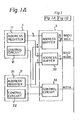
- a central processing unit (hereinafter referred to as a CPU) 1 and a channel control unit (hereinafter referred to as a CHC) 2 serve as access sources for a memory unit 4 through a memory access control unit (hereinafter referred to as an MAC) 3.
- a CPU central processing unit
- CHC channel control unit
- MAC memory access control unit
- an address code of sixteen bits is transmitted from an address register 11 or 21 of the CPU 1 or CHC 2 to the MAC 3.
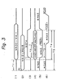
- the lower order seven bits of the address code are supplied to an address buffer 32 of the MAC 3 which produces seven signals MA12 through MA18, as indicated shown in Fig. 3(2), without modification, while the higher order nine bits of the address code are supplied to an address mapper 31 of the MAC 3, which produces twelve signals MA00 through MA11, as indicated in Fig.
- Fig. 3(1 T1 is a time which is necessary for modifying nine bits of the address code to the twelve signals MA00 through MA11.
- the signals MA12 through MA18 are supplied to a memory address register (hereinafer referred to as an MAR) 41-2 of the memory unit 4 and, after that, at time t" the signals MA00 through MA11 are supplied to an MAR 41-1.
- a memory starting signal MSTA is supplied from a control circuit 33 of the MAC 3, which is also controlled by a control circuit 12 or 22 of the CPU 1 or CHC 2, to a control circuit 42 of the memory unit 4, as indicated in Fig. 3(3).
- the five signals MA00 through MA04 are supplied to a decoder 43 for selecting one module from thirty-two memory modules 47-0 through 47-31.
- the seven signals MA12 'through MA18 are transmitted from the MAR41-2 to the selected memory module and, after that, at time t 2 , the seven signals MA05 through MA11 are transmitted from the MAR 41-1 to the selected memory module, as indicated in Fig. 3(4).
- Such time divisional transmission is effected by a multiplexer 44 which is controlled by a control circuit 46, which receives the control signal MSTA through a delay circuit 45 whose delay time is T2, and each of the memory modules 47-0 through 47-31 has address input pins common for the signals MA05 through MA11 and the signals MA12 through MA18.
- the address mapper 31 comprises a random access memory (RAM) from which is read out data of twelve bits by using an address code of nine bits.
- the control signal TRAS is the same as the control signal MSTA, while the control siganl TCAS is obtained by delaying the control signal MSTA.
- the delay time T3 (Fig. 3) is determined by a delay circuit 421.
- the potential of a control signal from the decoder 43 is high, so that a row access signal * RAS is the same as a control signal TRAS (which is an inverted signal of the signal TRAS) through a gate G1 as indicated in Fig.
- a column access signal * CAS is the same as a control signal TCAS (which is an inverted signal of the signal TCAS) through a gate G2 as indicated in Fig. 3(6).
- TCAS which is an inverted signal of the signal TCAS
- the signals MA12 through MA18 are applied to a cell array 471 in syncronization with the control signal * RAS and, after that, the signals MA05 through MA1 are applied to the cell array 471 in syncronization with the control signal * CAS.
- the total access time T5 (Fig. 3) is determined by the sum of the modification time T1 and the actual access time T4, which means that the access speed is low.
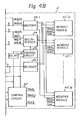
- Fig. 4 is a block diagram illustrating an embodiment of the system for accessing memory modules of the present invention.
- the elements illustrated in Fig. 4 which are identical to those of Fig. 1 are denoted by the same reference numerals.
- the control circuit 33' of the MAC 3 produces two kinds of memory starting signals MSTA1 and MSTA2.
- the memory unit 4' comprises three MARs 41 ⁇ 1, 41 ⁇ 2 and 41 ⁇ 3, two decoders 43 ⁇ 1 and 43-2, and a comparator circuit 48.
- the control circuit 42' of the memory unit 4' produces three kinds of control signals TRAS1, TRAS2 and TCAS.
- the control circuit 42' will now be explained in more detail.
- Fig. 5 is a block diagram of the control circuit 42' of Fig. 4.
- the control circuit 42' comprises two control circuits 422 and 423 used mainly for refreshing dynamic memories, such as memory modules 47'-0 through 47'-31, two gates G3 and G4 controlled by the comparator circuit 48 (Fig. 4), two delay circuits 424 and 425 whose delay time is T3 and a gate G5.
- the potentials of two signals C1 and C2 are low, so that the gates G3 and G4 are closed.
- the signal TRAS1 also becomes high.
- the comparator circuit 48 (Fig.
- the comparator circuit 48 begins to operate, so that the comparator circuit 48 raises either the potential of the signal C1 or the potential of the signal C2.
- the signal TCAS is obtained by delaying the signal TRAS1 due to the presence of the delay circuit 424, whose delay time is T3.
- the signal TCAS is obtained by delaying the signal TRAS2 due to the presence of the delay circuit 425, whose delay time is also T3.
- the memory module 47'-i comprises a gate G6 for receiving signals from the decoders 43-1 and 43-2 (Fig. 4), two gates G7 and G8 for passing the signals TRAS1 and TRAS2, respectively, a gate G9 for generating a signal * RAS to a cell array 471 and a gate G10 for passing the signal TCAS.
- the signal TRAS 1 passes through the gates G7 and G9, so that the signal * RAS is the same as an inverted signal of the signal TRAS1.
- the signal TCAS passes through the gate G 10, so that the signal * CAS is the same as an inverted signal of the signal TCAS.
- the signal TRAS2 passes through the gates G8 and G9, so that the signal * RAS is the same as an inverted signal of the signal TRAS2.
- the signal TCAS is blocked by the gate G10.
- the signal TCAS passes through the gate G10, so that the signal * CAS is the same as an inverted signal of the signal TCAS.
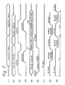
- Figs. 7(1) through 7(9) are timing diagrams indicating the signals appearing in the circuits of Figs. 4, 5 and 6. In more detail, these figures are as follows.
- Fig. 7(1) indicates the signals MA00 through MA11, which are output from the address mapper 31;
- Fig. 7(2) indicates the signals MA12 through MA18, which are output from the address buffer 32;
- Figs. 7(3) and 7(4) indicate the memory starting signals MSTA1 and MSTA2, respectively, which are output from the control circuit 33';
- Fig. 7(5) indicates the signals, which are output from the multiplexer 44;
- Figs. 7(6) and 7(7) indicate the signals * RAS and * CAS in the memory module 47'-2, and;
- Figs. 7(8) and 7(9) indicate the signals * RAS and * CAS in the memory module 47'-1.
- Figs. 8(1) through 8(7) are block diagrams of the memory address registers 41-1, 41-2 and 41-3, for explaining the operation of the circuits of Figs. 4, 5 and 6. Referring to Figs. 7(1) through 7(9) and Figs. 8(1) through 8(7), the operations of the circuits of Figs. 4, 5 and 6 are as follows.
- the total access time which is denoted by T6 in Fig. 7(9)
- the total access time which is indicated by T7
- an executive program consists of routine programs, each of which may be stored in one memory module. Therefore, the higher order five bits of the MAR 41-1, which designate the selection of the memory modules, often coincide with those of the MAR 41-3. As a result, the average access time is nearly T7, which is very short.
- the system for accessing memory modules according to the present invention has the advantage that the access time is very short, in other words, that the access speed is higher than that of the prior art, since before an entire current effective address is determined, the actual access for the memory modules is executed by using a part of the previous effective address.
Landscapes
- Engineering & Computer Science (AREA)
- Theoretical Computer Science (AREA)
- Physics & Mathematics (AREA)
- General Engineering & Computer Science (AREA)
- General Physics & Mathematics (AREA)
- Static Random-Access Memory (AREA)
- Memory System Of A Hierarchy Structure (AREA)
- Memory System (AREA)
- Dram (AREA)
Abstract
Claims (4)
Applications Claiming Priority (2)
| Application Number | Priority Date | Filing Date | Title |
|---|---|---|---|
| JP37885/79 | 1979-03-30 | ||
| JP54037885A JPS5943786B2 (ja) | 1979-03-30 | 1979-03-30 | 記憶装置のアクセス方式 |
Publications (3)
| Publication Number | Publication Date |
|---|---|
| EP0025801A4 EP0025801A4 (fr) | 1981-03-09 |
| EP0025801A1 EP0025801A1 (fr) | 1981-04-01 |
| EP0025801B1 true EP0025801B1 (fr) | 1983-05-11 |
Family
ID=12509989
Family Applications (1)
| Application Number | Title | Priority Date | Filing Date |
|---|---|---|---|
| EP80900611A Expired EP0025801B1 (fr) | 1979-03-30 | 1980-10-23 | Systeme d'acces pour des modules de memoire |
Country Status (8)
| Country | Link |
|---|---|
| US (1) | US4384342A (fr) |
| EP (1) | EP0025801B1 (fr) |
| JP (1) | JPS5943786B2 (fr) |
| AU (1) | AU515171B2 (fr) |
| CA (1) | CA1127318A (fr) |
| DE (1) | DE3063041D1 (fr) |
| ES (1) | ES8103868A1 (fr) |
| WO (1) | WO1980002206A1 (fr) |
Families Citing this family (28)
| Publication number | Priority date | Publication date | Assignee | Title |
|---|---|---|---|---|
| US5526506A (en) * | 1970-12-28 | 1996-06-11 | Hyatt; Gilbert P. | Computer system having an improved memory architecture |
| US5459846A (en) * | 1988-12-02 | 1995-10-17 | Hyatt; Gilbert P. | Computer architecture system having an imporved memory |
| JPS57164484A (en) * | 1981-03-31 | 1982-10-09 | Fujitsu Ltd | Replace system |
| JPS58214954A (ja) * | 1982-06-09 | 1983-12-14 | Nec Corp | 大容量デ−タ記憶システム |
| JPS5932045A (ja) * | 1982-08-16 | 1984-02-21 | Hitachi Ltd | 情報処理装置 |
| US4649476A (en) * | 1983-10-31 | 1987-03-10 | Motorola, Inc. | Microcomputer having an internal address mapper |
| US4652993A (en) * | 1984-04-02 | 1987-03-24 | Sperry Corporation | Multiple output port memory storage module |
| US4742451A (en) * | 1984-05-21 | 1988-05-03 | Digital Equipment Corporation | Instruction prefetch system for conditional branch instruction for central processor unit |
| JPS6140657A (ja) * | 1984-08-01 | 1986-02-26 | Yaskawa Electric Mfg Co Ltd | 低速メモリの高速アクセス方式 |
| US4817036A (en) * | 1985-03-15 | 1989-03-28 | Brigham Young University | Computer system and method for data base indexing and information retrieval |
| US4761731A (en) * | 1985-08-14 | 1988-08-02 | Control Data Corporation | Look-ahead instruction fetch control for a cache memory |
| JPS6293249U (fr) * | 1985-11-29 | 1987-06-15 | ||
| JPS62149099A (ja) * | 1985-12-23 | 1987-07-03 | Toshiba Corp | メモリアクセス制御回路 |
| EP0232518A3 (fr) * | 1986-01-13 | 1989-12-13 | Siemens Aktiengesellschaft | Procédé et système de formation d'adresses pour commander une mémoire de travail |
| US4893279A (en) * | 1986-03-04 | 1990-01-09 | Advanced Micro Devices Inc. | Storage arrangement having a pair of RAM memories selectively configurable for dual-access and two single-access RAMs |
| JPS635444A (ja) * | 1986-06-25 | 1988-01-11 | Hitachi Ltd | マイクロプロセツサ |
| US4884198A (en) * | 1986-12-18 | 1989-11-28 | Sun Microsystems, Inc. | Single cycle processor/cache interface |
| IT1216087B (it) * | 1988-03-15 | 1990-02-22 | Honeywell Bull Spa | Sistema di memoria con selezione predittiva di modulo. |
| US5301278A (en) * | 1988-04-29 | 1994-04-05 | International Business Machines Corporation | Flexible dynamic memory controller |
| GB2246001B (en) * | 1990-04-11 | 1994-06-15 | Digital Equipment Corp | Array architecture for high speed cache memory |
| US5283875A (en) * | 1990-04-13 | 1994-02-01 | Digital Equipment Corporation | Method and apparatus for optimizing prefetch caching by reverse ordering of logical blocks |
| US5317708A (en) * | 1990-06-29 | 1994-05-31 | Digital Equipment Corporation | Apparatus and method for an improved content addressable memory |
| GB9023339D0 (en) * | 1990-10-26 | 1990-12-05 | Ici Plc | Dispensing of fluids |
| US5575636A (en) * | 1994-06-21 | 1996-11-19 | Praxair Technology, Inc. | Porous non-fouling nozzle |
| US5530836A (en) * | 1994-08-12 | 1996-06-25 | International Business Machines Corporation | Method and apparatus for multiple memory bank selection |
| US5835932A (en) * | 1997-03-13 | 1998-11-10 | Silicon Aquarius, Inc. | Methods and systems for maintaining data locality in a multiple memory bank system having DRAM with integral SRAM |
| US7143185B1 (en) * | 2000-08-29 | 2006-11-28 | Advanced Micro Devices, Inc. | Method and apparatus for accessing external memories |
| US20060212658A1 (en) * | 2005-03-18 | 2006-09-21 | International Business Machines Corporation. | Prefetch performance of index access by look-ahead prefetch |
Family Cites Families (12)
| Publication number | Priority date | Publication date | Assignee | Title |
|---|---|---|---|---|
| US3504349A (en) * | 1967-09-27 | 1970-03-31 | Ibm | Address examination mechanism for use in a system operating with dynamic storage relocation |
| US3829840A (en) * | 1972-07-24 | 1974-08-13 | Ibm | Virtual memory system |
| FR121860A (fr) * | 1973-07-19 | |||
| US4156905A (en) * | 1974-02-28 | 1979-05-29 | Ncr Corporation | Method and apparatus for improving access speed in a random access memory |
| JPS5169333A (en) * | 1974-12-13 | 1976-06-15 | Fujitsu Ltd | Peeji adoresuseigyohoshiki |
| JPS5216137A (en) * | 1975-07-29 | 1977-02-07 | Nippon Telegr & Teleph Corp <Ntt> | Main memory access control system |
| IT1052771B (it) * | 1975-12-31 | 1981-07-20 | Olivetti C E C S P A | Dispositivo di indirizzamento di una memoria |
| GB2003302B (en) * | 1977-08-24 | 1982-02-10 | Ncr Co | Random access memory system |
| US4296467A (en) * | 1978-07-03 | 1981-10-20 | Honeywell Information Systems Inc. | Rotating chip selection technique and apparatus |
| FR2443723A1 (fr) * | 1978-12-06 | 1980-07-04 | Cii Honeywell Bull | Dispositif de reduction du temps d'acces aux informations contenues dans une memoire d'un systeme de traitement de l'information |
| US4303993A (en) * | 1979-10-10 | 1981-12-01 | Honeywell Information Systems Inc. | Memory present apparatus |
| US4323965A (en) * | 1980-01-08 | 1982-04-06 | Honeywell Information Systems Inc. | Sequential chip select decode apparatus and method |
-
1979
- 1979-03-30 JP JP54037885A patent/JPS5943786B2/ja not_active Expired
-
1980
- 1980-03-13 CA CA347,613A patent/CA1127318A/fr not_active Expired
- 1980-03-24 AU AU56781/80A patent/AU515171B2/en not_active Expired
- 1980-03-28 DE DE8080900611T patent/DE3063041D1/de not_active Expired
- 1980-03-28 US US06/201,396 patent/US4384342A/en not_active Expired - Lifetime
- 1980-03-28 ES ES490033A patent/ES8103868A1/es not_active Expired
- 1980-08-28 WO PCT/JP1980/000054 patent/WO1980002206A1/fr not_active Ceased
- 1980-10-23 EP EP80900611A patent/EP0025801B1/fr not_active Expired
Also Published As
| Publication number | Publication date |
|---|---|
| WO1980002206A1 (fr) | 1980-10-16 |
| AU5678180A (en) | 1981-01-15 |
| ES490033A0 (es) | 1981-03-16 |
| JPS55129847A (en) | 1980-10-08 |
| US4384342A (en) | 1983-05-17 |
| ES8103868A1 (es) | 1981-03-16 |
| DE3063041D1 (en) | 1983-06-16 |
| EP0025801A4 (fr) | 1981-03-09 |
| EP0025801A1 (fr) | 1981-04-01 |
| CA1127318A (fr) | 1982-07-06 |
| JPS5943786B2 (ja) | 1984-10-24 |
| AU515171B2 (en) | 1981-03-19 |
Similar Documents
| Publication | Publication Date | Title |
|---|---|---|
| US4384342A (en) | System for reducing access time to plural memory modules using five present-fetch and one prefetch address registers | |
| US4953128A (en) | Variable delay circuit for delaying input data | |
| EP0138964B1 (fr) | Dispositif de commande de l'acces a une memoire | |
| EP0263924B1 (fr) | Structure de réarrangement de bits sur une puce | |
| KR910002501B1 (ko) | 에러 교정회로를 갖는 반도체 기억장치 | |
| US4359771A (en) | Method and apparatus for testing and verifying the operation of error control apparatus within a memory | |
| US4369510A (en) | Soft error rewrite control system | |
| US4839856A (en) | Memory access control circuit | |
| EP0549139A1 (fr) | Temporisation programmable pour mémoire | |
| US5093783A (en) | Microcomputer register bank accessing | |
| EP0096782A2 (fr) | Réalignement on-line d'erreurs de mémoire | |
| US5572692A (en) | Memory configuration decoding system having automatic row base address generation mechanism for variable memory devices with row access interleaving | |
| JPH0255878B2 (fr) | ||
| KR840001731A (ko) | 순차적인 워어드가 정열된 어드레스 지정장치 | |
| US4156290A (en) | Speedup addressing device by detecting repetitive addressing | |
| US4376972A (en) | Sequential word aligned address apparatus | |
| US5315553A (en) | Memory circuit test system using separate ROM having test values stored therein | |
| KR950014551B1 (ko) | 반도체기억장치 및 그 출력제어방법 | |
| US4731738A (en) | Memory timing and control apparatus | |
| US5479640A (en) | Memory access system including a memory controller with memory redrive circuitry | |
| US5550996A (en) | ROM burst transfer continuous read-out extension method and a microcomputer system with a built-in ROM using this method | |
| US4424562A (en) | Data processing system having plural address arrays | |
| US5410514A (en) | Single clock memory having a page mode | |
| JPH1069430A (ja) | 半導体記憶装置 | |
| US5602782A (en) | Pipeline-operating type memory system capable of reading data from a memory array having data width larger than the output data width |
Legal Events
| Date | Code | Title | Description |
|---|---|---|---|
| PUAI | Public reference made under article 153(3) epc to a published international application that has entered the european phase |
Free format text: ORIGINAL CODE: 0009012 |
|
| 17P | Request for examination filed |
Effective date: 19801027 |
|
| AK | Designated contracting states |
Designated state(s): DE FR GB NL |
|
| GRAA | (expected) grant |
Free format text: ORIGINAL CODE: 0009210 |
|
| AK | Designated contracting states |
Designated state(s): DE FR GB NL |
|
| REF | Corresponds to: |
Ref document number: 3063041 Country of ref document: DE Date of ref document: 19830616 |
|
| ET | Fr: translation filed | ||
| PLBE | No opposition filed within time limit |
Free format text: ORIGINAL CODE: 0009261 |
|
| STAA | Information on the status of an ep patent application or granted ep patent |
Free format text: STATUS: NO OPPOSITION FILED WITHIN TIME LIMIT |
|
| 26N | No opposition filed | ||
| PGFP | Annual fee paid to national office [announced via postgrant information from national office to epo] |
Ref country code: FR Payment date: 19990309 Year of fee payment: 20 |
|
| PGFP | Annual fee paid to national office [announced via postgrant information from national office to epo] |
Ref country code: NL Payment date: 19990329 Year of fee payment: 20 |
|
| PGFP | Annual fee paid to national office [announced via postgrant information from national office to epo] |
Ref country code: GB Payment date: 19990401 Year of fee payment: 20 |
|
| PGFP | Annual fee paid to national office [announced via postgrant information from national office to epo] |
Ref country code: DE Payment date: 19990406 Year of fee payment: 20 |
|
| PG25 | Lapsed in a contracting state [announced via postgrant information from national office to epo] |
Ref country code: GB Free format text: LAPSE BECAUSE OF EXPIRATION OF PROTECTION Effective date: 20000327 |
|
| PG25 | Lapsed in a contracting state [announced via postgrant information from national office to epo] |
Ref country code: NL Free format text: LAPSE BECAUSE OF EXPIRATION OF PROTECTION Effective date: 20000328 |
|
| REG | Reference to a national code |
Ref country code: GB Ref legal event code: PE20 Effective date: 20000327 |
|
| NLV7 | Nl: ceased due to reaching the maximum lifetime of a patent |
Effective date: 20000328 |