EP0028657B1 - Hohle, gedruckte vielschichtschalttafel und verfahren zu deren herstellung - Google Patents
Hohle, gedruckte vielschichtschalttafel und verfahren zu deren herstellung Download PDFInfo
- Publication number
- EP0028657B1 EP0028657B1 EP80900951A EP80900951A EP0028657B1 EP 0028657 B1 EP0028657 B1 EP 0028657B1 EP 80900951 A EP80900951 A EP 80900951A EP 80900951 A EP80900951 A EP 80900951A EP 0028657 B1 EP0028657 B1 EP 0028657B1
- Authority
- EP
- European Patent Office
- Prior art keywords
- substrate
- resist
- conductor pattern
- conductor
- pattern
- Prior art date
- Legal status (The legal status is an assumption and is not a legal conclusion. Google has not performed a legal analysis and makes no representation as to the accuracy of the status listed.)
- Expired
Links
Images




Classifications
-
- H—ELECTRICITY
- H05—ELECTRIC TECHNIQUES NOT OTHERWISE PROVIDED FOR
- H05K—PRINTED CIRCUITS; CASINGS OR CONSTRUCTIONAL DETAILS OF ELECTRIC APPARATUS; MANUFACTURE OF ASSEMBLAGES OF ELECTRICAL COMPONENTS
- H05K3/00—Apparatus or processes for manufacturing printed circuits
- H05K3/46—Manufacturing multilayer circuits
- H05K3/4611—Manufacturing multilayer circuits by laminating two or more circuit boards
- H05K3/4614—Manufacturing multilayer circuits by laminating two or more circuit boards the electrical connections between the circuit boards being made during lamination
- H05K3/462—Manufacturing multilayer circuits by laminating two or more circuit boards the electrical connections between the circuit boards being made during lamination characterized by laminating only or mainly similar double-sided circuit boards
-
- H—ELECTRICITY
- H05—ELECTRIC TECHNIQUES NOT OTHERWISE PROVIDED FOR
- H05K—PRINTED CIRCUITS; CASINGS OR CONSTRUCTIONAL DETAILS OF ELECTRIC APPARATUS; MANUFACTURE OF ASSEMBLAGES OF ELECTRICAL COMPONENTS
- H05K3/00—Apparatus or processes for manufacturing printed circuits
- H05K3/40—Forming printed elements for providing electric connections to or between printed circuits
- H05K3/42—Plated through-holes or plated via connections
- H05K3/429—Plated through-holes specially for multilayer circuits, e.g. having connections to inner circuit layers
-
- H—ELECTRICITY
- H05—ELECTRIC TECHNIQUES NOT OTHERWISE PROVIDED FOR
- H05K—PRINTED CIRCUITS; CASINGS OR CONSTRUCTIONAL DETAILS OF ELECTRIC APPARATUS; MANUFACTURE OF ASSEMBLAGES OF ELECTRICAL COMPONENTS
- H05K1/00—Printed circuits
- H05K1/02—Details
- H05K1/0272—Adaptations for fluid transport, e.g. channels, holes
-
- H—ELECTRICITY
- H05—ELECTRIC TECHNIQUES NOT OTHERWISE PROVIDED FOR
- H05K—PRINTED CIRCUITS; CASINGS OR CONSTRUCTIONAL DETAILS OF ELECTRIC APPARATUS; MANUFACTURE OF ASSEMBLAGES OF ELECTRICAL COMPONENTS
- H05K1/00—Printed circuits
- H05K1/02—Details
- H05K1/03—Use of materials for the substrate
- H05K1/05—Insulated conductive substrates, e.g. insulated metal substrate
- H05K1/053—Insulated conductive substrates, e.g. insulated metal substrate the metal substrate being covered by an inorganic insulating layer
-
- H—ELECTRICITY
- H05—ELECTRIC TECHNIQUES NOT OTHERWISE PROVIDED FOR
- H05K—PRINTED CIRCUITS; CASINGS OR CONSTRUCTIONAL DETAILS OF ELECTRIC APPARATUS; MANUFACTURE OF ASSEMBLAGES OF ELECTRICAL COMPONENTS
- H05K2201/00—Indexing scheme relating to printed circuits covered by H05K1/00
- H05K2201/03—Conductive materials
- H05K2201/0332—Structure of the conductor
- H05K2201/0364—Conductor shape
- H05K2201/0379—Stacked conductors
-
- H—ELECTRICITY
- H05—ELECTRIC TECHNIQUES NOT OTHERWISE PROVIDED FOR
- H05K—PRINTED CIRCUITS; CASINGS OR CONSTRUCTIONAL DETAILS OF ELECTRIC APPARATUS; MANUFACTURE OF ASSEMBLAGES OF ELECTRICAL COMPONENTS
- H05K2201/00—Indexing scheme relating to printed circuits covered by H05K1/00
- H05K2201/09—Shape and layout
- H05K2201/09209—Shape and layout details of conductors
- H05K2201/095—Conductive through-holes or vias
- H05K2201/09536—Buried plated through-holes, i.e. plated through-holes formed in a core before lamination
-
- H—ELECTRICITY
- H05—ELECTRIC TECHNIQUES NOT OTHERWISE PROVIDED FOR
- H05K—PRINTED CIRCUITS; CASINGS OR CONSTRUCTIONAL DETAILS OF ELECTRIC APPARATUS; MANUFACTURE OF ASSEMBLAGES OF ELECTRICAL COMPONENTS
- H05K2201/00—Indexing scheme relating to printed circuits covered by H05K1/00
- H05K2201/09—Shape and layout
- H05K2201/09209—Shape and layout details of conductors
- H05K2201/095—Conductive through-holes or vias
- H05K2201/096—Vertically aligned vias, holes or stacked vias
-
- H—ELECTRICITY
- H05—ELECTRIC TECHNIQUES NOT OTHERWISE PROVIDED FOR
- H05K—PRINTED CIRCUITS; CASINGS OR CONSTRUCTIONAL DETAILS OF ELECTRIC APPARATUS; MANUFACTURE OF ASSEMBLAGES OF ELECTRICAL COMPONENTS
- H05K2203/00—Indexing scheme relating to apparatus or processes for manufacturing printed circuits covered by H05K3/00
- H05K2203/03—Metal processing
- H05K2203/0315—Oxidising metal
-
- H—ELECTRICITY
- H05—ELECTRIC TECHNIQUES NOT OTHERWISE PROVIDED FOR
- H05K—PRINTED CIRCUITS; CASINGS OR CONSTRUCTIONAL DETAILS OF ELECTRIC APPARATUS; MANUFACTURE OF ASSEMBLAGES OF ELECTRICAL COMPONENTS
- H05K3/00—Apparatus or processes for manufacturing printed circuits
- H05K3/40—Forming printed elements for providing electric connections to or between printed circuits
- H05K3/42—Plated through-holes or plated via connections
- H05K3/425—Plated through-holes or plated via connections characterised by the sequence of steps for plating the through-holes or via connections in relation to the conductive pattern
- H05K3/426—Plated through-holes or plated via connections characterised by the sequence of steps for plating the through-holes or via connections in relation to the conductive pattern initial plating of through-holes in substrates without metal
-
- H—ELECTRICITY
- H05—ELECTRIC TECHNIQUES NOT OTHERWISE PROVIDED FOR
- H05K—PRINTED CIRCUITS; CASINGS OR CONSTRUCTIONAL DETAILS OF ELECTRIC APPARATUS; MANUFACTURE OF ASSEMBLAGES OF ELECTRICAL COMPONENTS
- H05K3/00—Apparatus or processes for manufacturing printed circuits
- H05K3/40—Forming printed elements for providing electric connections to or between printed circuits
- H05K3/42—Plated through-holes or plated via connections
- H05K3/425—Plated through-holes or plated via connections characterised by the sequence of steps for plating the through-holes or via connections in relation to the conductive pattern
- H05K3/427—Plated through-holes or plated via connections characterised by the sequence of steps for plating the through-holes or via connections in relation to the conductive pattern initial plating of through-holes in metal-clad substrates
-
- H—ELECTRICITY
- H05—ELECTRIC TECHNIQUES NOT OTHERWISE PROVIDED FOR
- H05K—PRINTED CIRCUITS; CASINGS OR CONSTRUCTIONAL DETAILS OF ELECTRIC APPARATUS; MANUFACTURE OF ASSEMBLAGES OF ELECTRICAL COMPONENTS
- H05K3/00—Apparatus or processes for manufacturing printed circuits
- H05K3/46—Manufacturing multilayer circuits
- H05K3/4611—Manufacturing multilayer circuits by laminating two or more circuit boards
- H05K3/4623—Manufacturing multilayer circuits by laminating two or more circuit boards the circuit boards having internal via connections between two or more circuit layers before lamination, e.g. double-sided circuit boards
-
- Y—GENERAL TAGGING OF NEW TECHNOLOGICAL DEVELOPMENTS; GENERAL TAGGING OF CROSS-SECTIONAL TECHNOLOGIES SPANNING OVER SEVERAL SECTIONS OF THE IPC; TECHNICAL SUBJECTS COVERED BY FORMER USPC CROSS-REFERENCE ART COLLECTIONS [XRACs] AND DIGESTS
- Y10—TECHNICAL SUBJECTS COVERED BY FORMER USPC
- Y10T—TECHNICAL SUBJECTS COVERED BY FORMER US CLASSIFICATION
- Y10T29/00—Metal working
- Y10T29/49—Method of mechanical manufacture
- Y10T29/49002—Electrical device making
- Y10T29/49117—Conductor or circuit manufacturing
- Y10T29/49124—On flat or curved insulated base, e.g., printed circuit, etc.
- Y10T29/49126—Assembling bases
Definitions
- This invention relates to a hollow multilayer printed wiring board and a process for manufacturing the multilayer printed wiring board.
- a hollow multilayer printed wiring board used herein is meant a multilayer printed wiring board which comprises at least two insulating material substrates, on each of which a conductor pattern or patterns are formed, the conductor pattern or patterns being interconnected as may be required, and each of which substrate is spaced apart a predetermined distance from the adjacent substrate or substrates, said space being filled with an insulative gas or liquid.
- Most conventional multilayer printed wiring boards are prepared by laminating substrates, having formed thereon conductor patterns, by interposing an adhesive layer comprised of glass fibres impregnated with a prepolymer of a thermosetting resin between the substrates.
- the adhesive layer used must satisfy many requirements, such as good thermal resistance, low shrinkage upon curing and good moldability. With an increase in the packaging density, it becomes more and more difficult to manufacture the composite structure by using the adhesive layer of thermosetting resin-impregnated glass fibres.
- the main object of the present invention to provide multilayer printed wiring boards which exhibit good thermal resistance, as well as enhanced dimensional stability, and improved transmission and cooling characteristics, as compared with the prior art.
- a hollow multilayer printed wiring board which comprises a plurality of superposed substrates each substrate having a signal conductor pattern formed on at least one surface thereof and a land conductor pattern formed on at least one surface thereof, and said substrates being superposed upon each other with a predetermined space therebetween filled with an insulative gas or liquid, and each substrate having plated through holes in the land conductor pattern, eacti of which plated through holes is in line with another plated through hole of each of the neighbouring substrates or of at least one of the neighbouring substrates, each of which plated through holes comprises a first through hole conductor plating layer formed on the inner walls of the through holes and on at least part of the land conductor pattern and a second through hole plating layer of a low melting point metal formed at least on the upper and lower end surfaces of the first through hole conductor plating layer, which second through hole plating layer serves as a through connection between two or more signal conductor patterns of the substrates and as an interlayer adhesion between the substrates, and the
- first and second processes for manufacturing a hollow multilayer printed wiring board as defined in the preceding paragraph and claimed in claim 1.
- the aforesaid first process comprises the steps of preparing a plurality of printed substrates made of a thermally resistant organic synthetic resin or a thermally resistant inorganic material, each substrate having a signal conductor pattern formed on at least one surface thereof and a land conductor pattern on at least one surface thereof and further having plated through holes in the land conductor pattern, a layer of a low melting point metal being formed at least on the upper and lower end surfaces of each of plating layers formed on the plated through holes, and either covering said signal conductor pattern with a ground conductor pattern electrically isolated from the signal conductor pattern and formed on the same surface of the substrate as that on which the signal conductor pattern is formed, or so forming said signal conductor pattern that it is sandwiched between conductors of a first, ground conductor pattern electrically isolated from the signal conductor pattern and formed on the same surface of the substrate as that on which said signal conductor
- the aforesaid second process comprises the steps of preparing a plurality of printed substrates made of a thermally resistant organic synthetic resin or a thermally resistant inorganic material, each substrate having a signal conductor pattern on at least one surface thereof and a land conductor pattern on at least one surface thereof, and further having a layer of a low melting point metal formed on said land conductor pattern, either covering said signal conductor pattern with a ground conductor pattern electrically isolated from the signal conductor pattern and formed on the same surface of the substrate as that on which the signal conductor pattern is formed, or so forming said signal conductor pattern that it is sandwiched between conductors of a first ground conductor pattern electrically isolated from the signal conductor pattern and formed on the same surface of the substrate as that on which said signal conductor pattern is formed, and covering said signal conductor pattern with a second ground conductor pattern electrically isolated from the signal conductor pattern and formed on the confronting surface of the substrate or a spacer adjacent to the substrate having the signal conductor pattern, and said second ground conductor pattern having an
- the substrates used for the construction of the hollow multilayer printed wiring board of the invention are made of a thermally resistant organic synthetic resin sheet or an insulation-treated metal sheet.
- the organic synthetic resin used includes, for example, a polyimide resin, an epoxy resin and a triazine resin.
- the insulation-treated metal used includes, for example, anodically oxidized metals, such as anodically oxidized aluminum, magnesium, titanium and thallium, and; metal sheets having insulation material layers deposited thereon, such as an iron sheet coated with an organic synthetic resin or an inorganic insulating material and an iron sheet sputtered with a non-conductive material.
- the most preferable insulation-treated metals are those which are prepared by anodically oxidizing a metal and, then, depositing an insulation material layer on the anodically oxidized metal.
- an anodically oxidized insulation layer is homogeneous.
- an insulation layer formed by coating or sputtering exhibits poor homogeneity, although it can be made desirably thick.
- the insulation-treated metals prepared by the combination of anodic oxidation with deposition of an insulation material layer are advantageous in that the insulation layer is relatively homogeneous and can be made into the desired thickness.
- a through connection between the two or more conductor patterns and an interlayer adhesion between the superposed substrates are achieved by using a low melting point metal.
- a low melting point metal used herein is meant a metal which possesses a melting point lower than the temperature at which the substrate is adversely affected to a considerable extent.
- the low melting metal includes, for example, a simple metal such as gold and tin and alloys such as tin-lead, cadmium-zinc, tin-lead-silver, lead-silver, tin-zinc and cadmium-silver.
- FIGS. 1A to 1D exemplifies the hereinbefore mentioned first process wherein plated through holes are formed in printed substrates made of a thermally resistant organic synthetic resin and, then, the printed substrates are superposed upon each other.
- a ceramic substrate 1 is used as the surface substrate, and two intermediate substrates 2 and 4 made of a thermally resistant organic synthetic resin, such as a polyimide or an epoxy resin, are positioned so that a spacer 3 made of a similar organic synthetic resin is interposed between them.
- Each of the substrates 1, 2 and 4 has a signal conductor pattern 6 on at least one surface thereof and a land conductor pattern 7 on at least one surface thereof.
- the spacer 3 has land conductor patterns 7 on both surfaces thereof.
- the signal conductor pattern 6 formed on the lower surface of the substrate 2 is sandwiched between conductors of a first ground conductor pattern 8 electrically isolated from the signal conductor pattern 6 and formed on the same surface of the substrate on which the signal conductor pattern 6 is formed.
- the signal conductor pattern 6 formed on the lower surface of the substrate 2 is covered with a second ground conductor pattern 9, which is electrically isolated from the signal conductor pattern 6 and formed on the upper surface of the spacer 3 confronting the substrate 2.
- the second ground conductor pattern 9 has an area sufficient for covering the signal conductor pattern 6 and the conductors of the first ground conductor pattern 8, formed on the confronting surface of the substrate 2.
- through holes 10 are bored in the land conductor pattern 7 of each of the substrates 1, 2 and 4 and the spacer 3.
- the substrates and the spacer, having the through holes 10 perforated therein, are then subjected to electroless deposition to form a conductor deposition layer 11 over the entire surface of each substrate or spacer, including the inner walls of the through holes, so that the substrates and the spacer can be subjected to electroplating.
- an electroplating conductor layer (not shown) may be formed on the electroless deposition conductor layer 11.
- a plated resist 14 is formed by conventional means on the portions, on which no land conductor pattern has been formed, to a thickness greater than that of electroplating conductor layers to be later formed thereon. Then, a first through hole conductor plating layer 12 is formed on the inner walls of the through holes 10 and on at least part of the land conductor pattern 7. The first through hole conductor plating layer 12 serves as a through connection between signal conductor patterns and a support for the superposed substrates and spacer, when the substrates and spacer are superposed to construct the hollow multilayer printed wiring board. Thereafter, a second through hole plating layer 13 of a low melting point metal is formed on the first through hole conductor plating layer 12 while the plated resist 14 still remains.
- the second through hole plating layer 13 serves as a through connection between signal conductor patterns, a support for the superposed substrates and spacer, and an interlayer adhesion, when the substrates and spacer are superposed upon another. It also serves as a resist when each substrate or spacer is etched after the resist 14 is removed therefrom. It is preferable that the second through hole plating layer 13 have a thickness such that the second through hole plating layer 13 does not flow out when heat and pressure are applied thereto in the subsequent step of lamination. Usually, the thickness of the second plating layer 13 may be approximately 5 to 10 microns.
- the plated resist 14 (shown in FIG. 1C) is removed and, then, portions of the electroless deposition layer 11 (shown in FIG. 1C), which portions are not covered by the first and second through hole plating layers 12 and 13, are removed by means of flash etching.
- the substrates 1, 2 and 4 and the spacer 3 are correctly brought into superposed position by utilizing reference registering holes (not shown), which are previously formed in each of the substrates and spacer, and then, adhered together under the application of heat and pressure.
- the heat applied should be of a quantity sufficient to melt the second through hole plating layer 13.
- a side wall or walls 16 made of an organic synthetic resin or a metal are formed on the side periphery of the superposed substrates and spacer, thereby to seal the spaces between the superposed substrates and spacer.
- Each sealed space may be filled with an insulative liquid or gas, which serves as a cooling medium, in order to enhance the cooling performance of the hollow multilayer printed wiring board. If the dielectric constant of the liquid filled in the sealed spaces is suitably selected, it is possible to freely set not only the cooling performance but also the dielectric constant of the whole multilayer printed wiring board.
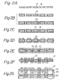
- FIGS. 2A to 2G illustrating the sequential steps of manufacturing the hollow multilayer printed wiring board from insulation-treated metal sheets, first, through holes 18 are bored in a metal sheet 17 by means of, for example, drilling, laser or chemical etching (FIG. 2A).
- the sheet 17 is made of a metal which is capable of being readily anodically oxidized, such as aluminum, magnesium, titanium or thallium.
- the entire surface of the bored metal sheet 17 including the inner walls of the through holes 18 is anodically oxidized to form an insulation film layer 19 serving a substrate for supporting a conductor pattern thereon (FIG. 2B, the upper figure).
- the insulation film layer 19 may be formed by depositing an insulation material onto the metal sheet, for example, by coating the metal sheet with an organic synthetic resin or an inorganic insulation material, or by sputtering the metal sheet.
- An optimum insulation-treated metal sheet is prepared by first anodically oxidizing the metal sheet to form the anodically oxidized insulation film layer 19 and, then, depositing an insulation material 20 thereon (FIG. 2B, the lower figure).
- a conductor layer 21 is formed on the entire surface of the insulation-treated metal sheet including the inner walls of the through holes 18 (FIG. 2C).
- the formation of the conductor layer 21 may be effected by conventional procedures, such as electroless deposition, printing, ion plating and vapor deposition. These procedures may be employed alone or in combination. If desired, the sheet having the conductor layer 21 formed thereon may be electroplated to increase the thickness of the conductor layer 21.
- the sheet is laminated with a photosensitive plastic resin or inorganic material layer, followed by pattern exposure and development, thereby to form a resist pattern 22 covering the portions other than those on which the intended conductor pattern is to be formed (FIG. 2D).
- a conductor layer 23 is formed on the region where resist does not exist, including the inner walls of the through holes by electroplating or printing (FIG. 2E). If desired, both surfaces of the conductor-formed sheet are subjected to a smoothing treatment. Then, a low melting point metal (not shown) is deposited onto the conductor layer 23 by electroplating, printing or vapor deposition.
- the resist 22 (shown in FIG. 2E) is removed and, then, the exposed portions of the conductor layer 21 (shown in FIG. 2E) are removed by means of flash etching to obtain a printed substrate 27 (FIG. 2F).
- the conductor layer 23 is formed by printing a conductor paste in the preceding fifth step, the printed conductor paste is dried, and then, the resist 22 and the portions of the conductor layer 21 are removed as mentioned above, and finally, the dried printed conductor paste is heated at a sintering temperature to form a metallized conductor layer 23.
- a plurality of the printed substrates 27 and one or more spacers 28 are superposed in a manner such that a spacer 28 is interposed between every two printed substrates 27.
- the superposed substrates and spacer or spacers are adhered together by applying either heat and pressure or laser, thereby melting the low melting point metal layer to obtain a hollow multilayer printed wiring board.
- the spacer 28 may be prepared in a manner similar to that mentioned above with reference to the preparation of the substrate 27.
- -the spaces 29 present between the superposed substrates may be sealed by forming a side wall or walls 30 on the side periphery of the hollow multilayer printed wiring board.
- the side wall or walls 30 may be bored in order to fill the sealed spaces with a suitable insulative gas or liquid.
- FIGS. 3A to 3B exemplifies the hereinbefore mentioned second process wherein printed substrates having no plated through holes are superposed upon each other and, then, plated through holes are bored in the superposed substrates.
- three substrates 31, 32 and 33 are used which are prepared from substrates each having conductor foils formed on both surfaces thereof.
- Each of the three substrates has a conductor pattern or patterns on at least one surface thereof.
- each of the two surface substrates 31 and 32 has a conductor foil 35 remaining on one surface thereof and a land conductor pattern 36 and a signal conductor pattern 37 on the other surface thereof.
- the intermediate substrate 33 has land conductor patterns 36 and signal conductor patterns 37 on both surfaces thereof.
- a plated layer 38 comprised of an alloy having a relatively high melting point is formed on all of the land conductor patterns 36.
- the three substrates 31, 32 and 33 are superposed upon another as shown in FIG. 3A, and then, adhered together by applying heat and pressure sufficient to melt the plated alloy layer 38. Thereafter, through holes 39 are bored in the superposed land conductor pattern portions 36 (FIG. 3B). Then, the adhered substrates are subjected to panel plating to deposit a conductor 40 on the inner walls of the through hole 39, and thereafter, the adhered substrates are subjected to plating with an alloy having a melting point 42 lower than that of the plated alloy layer 38. Then, the conductor foils 35 on the surfaces of the substrates 31 and 32 are etched to form surface signal conductor patterns 41. Whereby, a hollow multilayer printed wiring board of a closed type is obtained (FIG. 3C).
- At least one of the substrates located on the surfaces of the multilayer printed wiring board be made of an inorganic thermally resistant material, such as ceramics or an insulation-treated metal, as illustrated in FIGS. 1A, 3A and 4A (mentioned below). This is advantageous particularly where parts are directly bonded to the multilayer printed wiring board upon packaging.
- the substrates of the multilayer printed wiring board of the invention may be a non-hollow multilayer printed wiring board.
- FIG. 4C One example of the multilayer printed wiring board having as one substrate a non-hollow multilayer printed wiring board is illustrated in FIG. 4C.
- the hollow multilayer printed wiring board has a substrate of a non-hollow multilayer printed wiring board 68 of a thermally resistant organic resin material and a surface substrate 69 of ceramics, the two substrates being superposed upon each other with a predetermined space therebetween and bonded by low melting point metal layers 75 and through hole plating layers 76 formed on the inner walls of the through holes.
- the hollow multilayer printed wiring board of FIG. 4C is manufactured by the sequential steps illustrated in FIGS. 4A to 4C. Namely, a ceramic substrate having a conductor foil 67 formed on its upper surface and a land conductor pattern 71, a signal conductor pattern 70 and a first ground conductor pattern 72 formed on the lower surface is prepared (FIG. 4A). A non-hollow multilayer printed wiring board 68 having a land conductor pattern 71 and a second ground conductor pattern 72' formed on its upper surface and a conductor foil 67 formed on the lower surface is prepared (FIG. 4A). Both the ceramic substrate 69 and the multilayer printed wiring board 68 have through holes 73 bored in the land conductor patterns.
- the signal conductor pattern 70 formed on the lower surface of the substrate 69 is sandwiched between conductors of the first ground conductor pattern 72 electrically isolated from the signal conductor pattern 70 and formed on the same surface, and furthermore, the second ground conductor pattern 72' is formed on the upper surface of the multilayer printed wiring board 68 so that the ground conductor pattern 72' covers the signal conductor pattern 70.
- the confronting surfaces of the ceramic substrate 69 and the multilayer printed wiring board 68 are plated with a low melting point metal 75 on the land conductor patterns 71 and on the peripheral edge portions thereof, and then, the ceramic substrate 69 and the multilayer printed wiring board 68 are adhered to each other by applying pressure and heat thereto.
- the superposed ceramic substrate 69 and multilayer printed wiring board 68 are plated with a conductor on the inner walls and upper and lower end portions of the through holes 73 to form through hole plating conductor layers 76.
- surface signal conductor patterns 77 are formed on the upper surface of the ceramic substrate 69 and on the lower surface of the multilayer printed wiring board 68.
- the low melting point metal layer 75 forming the side peripheral wall of the superposed substrates serves as a barrier for preventing both an electrolyte used in the step of forming the through hole plating layers 76 and an etchant used in the step of forming the surface signal conductor patterns 77 from penetrating into the space between the two substrates.
- the hollow multilayer printed wiring board of the invention may be of one of the following two structures.
- the first structure is such that, as hereinbefore described with reference to FIGS. 1A and 4A, the signal conductor pattern formed on the surface of each substrate is sandwiched between conductors of a first ground conductor pattern electrically isolated from the signal conductor pattern and formed on the same surface of the substrate as that on which the signal conductor pattern is formed, and said signal conductor pattern is covered with a second ground conductor pattern electrically isolated from the signal conductor pattern and formed on the confronting surface of the substrate or spacer adjacent to the substrate having the signal conductor pattern; said second ground conductor pattern having an area sufficient for covering the signal conductor pattern and the conductors of the first ground conductor pattern.
- first structure is formed with respect to a portion of the signal conductor pattern 6 formed on the lower surface of the substrate 2
- similar structures may be formed with respect to other portions of the signal conductor pattern formed on the same surface of the substrate 2 or the signal conductor patterns formed on the other substrates.
- the second structure is such that the signal conductor pattern formed on at least one surface of each substrate is covered with a ground conductor pattern electrically isolated from the signal conductor pattern and formed on the same surface of the substrate as that on which the signal conductor pattern is formed.
- FIG. 11A a signal conductor pattern 62 formed on a substrate 61 is covered with a ground conductor pattern 64 formed on the same substrate 61.
- the signal conductor pattern 62 is electrically isolated from the ground conductor pattern 64, i.e., there is an air space 66 between the signal conductor pattern 62 and the ground conductor pattern 64.
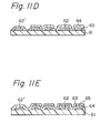
- the structure illustrated in FIG. 11A is manufactured by the sequential steps illustrated in FIGS. 11B to 11E.
- the substrate 61 having the signal conductor pattern 62 and a ground conductor pattern 62' formed on one surface thereof is prepared by a conventional patterning procedure (FIG. 11 B).
- a resist 63 is formed on the signal conductor pattern 62 by screen printing or another conventional coating or laminating procedure, which resist is soluble in a suitable solvent (FIG. 11 C).
- the ground conductor pattern 62' is not coated with the resist 63.
- the ground conductor pattern 64 is formed on the entire surface of the substrate 61 including the region coated with the resist 63 (FIG. 11D).
- the formation of the ground conductor pattern 64 may be effected by a conventional plating procedure.
- the ground conductor pattern 64 is etched by photoetching to form holes 65 for removing the resist 63 therethrough (FIG. 11E). Then, the resist 63 is dissolved in a solvent and removed through the holes 65, thereby to obtain a substrate of the structure illustrated in FIG. 11A. This substrate may be used as it is.
- the space 66 shown in FIG. IIA
- the ground conductor pattern 64 and the signal conductor pattern 62 may be filled with an insulating oil, which has a suitable dielectric constant and other electrical properties, and is chemically stable for impedance matching.
- the printed substrates used for manufacturing the hollow multilayer printed wiring board of the invention by the hereinbefore-mentioned second process i.e., the substrates each having a signal conductor pattern on at least one surface thereof and a land conductor pattern on at least one surface thereof, and further having a layer of a low melting point metal formed on said conductor pattern, but having no plated through holes, as illustrated in FIG. 3A, can be prepared by one of the following four processes.
- a first process comprises the steps of:
- a second process is similar to the above-mentioned first process except that the resist-formed substrate obtained by the step (i) is, prior to the step (ii), plated with a conductor to form plating conductor layers on the regions on which the signal conductor pattern and the land conductor pattern are to be formed.
- a third process comprises the steps of:
- a fourth process comprises the steps of:
- the printed substrates used for manufacturing the hollow multilayer printed board of the invention by the hereinbefore mentioned first process i.e., the substrates having a signal conductor pattern formed on at least one surface thereof and a land conductor pattern on at least one surface thereof and further having plated through holes in the land conductor pattern, layers of a low melting point metal being formed at least on the upper and lower end surfaces of each of the plating layers defining the plated through holes, can be prepared by one of the following processes.
- a first process comprises the steps of:
- FIGS. 2A through 2F One example of the above-mentioned first process is hereinbefore described with reference to FIGS. 2A through 2F.
- the steps (i) through (vii) in the above-mentioned first proess correspond to FIGS. 2A through 2F as follows.
- a second process is similar to the above-mentioned first process except that the step (v) of forming low melting point metal layers is carried out after the final etching step (vii). That is, the second process comprises the steps of:
- a third process comprises the steps of: (i) boring through holes in a land conductor pattern of a substrate having a signal conductor pattern on at least one surface thereof and the land conductor pattern on at least one surface thereof;
- FIGS. 1A through 1C One example of the above-mentioned third process is hereinbefore described with reference to FIGS. 1A through 1C.
- the steps (i) through (vii) in the above-mentioned third process correspond to FIGS. 1A to 1C as follows.
- a fourth process is similar to the above-mentioned third process except that the step (v) of forming low melting point metal layers is carried out after the final etching step (vii). That is, the fourth process comprises the steps of:
- a fifth process comprises the steps of:
- FIGS. 5A to 5F One example of the above-mentioned fifth process is illustrated in FIGS. 5A to 5F.
- a thermally resistant organic synthetic resin substrate 100 having conductor foils 100a on both surfaces thereof is prepared (FIG. 5A).
- a resist 101 is printed on the substrate 100 to form a resist pattern such that the conductor foils 100a are exposed in the portion 102, on which a signal conductor pattern is to be formed, and in the portions 103, on which lands and through holes are to be formed (FIG. 5B).
- Through holes 104 are formed.
- FIG. 5C The substrate is subjected to electroplating to form conductor layers 105 (FIG. 5D).
- the electroplated substrate is plated with a low melting point metal to form layers 106 of the low melting point metal on the electroplating conductor layers 105 (FIG. 5D).
- the resist 101 is removed (FIG. 5E).
- the substrate is subjected to flash etching to obtain a printed substrate P1 having a signal conductor pattern 107' and through hole plating layers 107 (FIG. 5F).
- the conductor 105 is not directly deposited on the inner walls 104a of the through holes 104, but the conductor 105 once deposited on the portions of the upper and lower conductor foils 100a surrounding the through holes 104 grows and finally covers the entire inner walls 104a as shown in FIG. 5D.
- a sixth process is similar to the above-mentioned fifth process except that the step (iv) of forming the low melting point metal layers is carried our after the final etching step (vi). That is, the sixth process comprises the steps of:
- a seventh process comprises the steps of:
- FIGS. 6A to 6F One example of the above-mentioned seventh process is illustrated in FIGS. 6A to 6F.
- a substrate 100 having conductor foils 100a on both surfaces thereof is prepared (FIG. 6A).
- a resist 101 is printed on the substrate 100 to form a resist pattern such that the conductor foils 100a are exposed only in the portion 102 on which a signal conductor pattern is to be formed (FIG. 6B).
- Through holes 104 are formed (FIG. 6C).
- the substrate is subjected to electroplating to form electroplating conductor layers 105 (FIG. 6D).
- the electroplated substrate is plated with a low melting point metal to form layers 106 of the low melting point metal on the electroplating conductor layers 105 (FIG.
- An eighth process is similar to the above-mentioned seventh process except that the step (iv) of forming the low melting point metal layers is carried out after the final etching step (vi). That is, the eighth process comprises the steps of:
- a ninth process comprises the steps of:
- FIGS. 7A to 7G One example of the above-mentioned ninth process is illustrated in FIGS. 7A to 7G.
- a substrate 100 having conductor foils 100a on both surfaces thereof is prepared (FIG. 7A).
- the substrate 100 is laminated with first photoresists (dry film) 101a a and then with second photoresists (dry film) 101b (FIG. 7B).
- the first photoresists 101a a have a property such that a conductor is capable of being deposited thereon by electroless deposition
- the second photoresists 101b have a property such that a conductor is incapable of being deposited thereon by electroless deposition.
- the photoresist-laminated substrate is light-exposed and then developed to form a resist pattern such that the conductor foils 100a are exposed in the portion 102 of the conductor foils on which a signal conductor pattern is to be formed (FIG. 7C).
- Through holes 104 are formed (FIG. 7D).
- the substrate is subjected to electroless plating to form conductor layers 109 on the exposed portions of the first photoresists 101a a (FIG. 7E).
- the substrate is subjected to electroplating twice to form first conductor plating layers 110 and low melting point metal plating layers 111 (FIG. 7F).
- the second resists 101b and the first resists 101a are removed, followed by flash etching, thereby to obtain a printed substrate P3 having a signal conductor pattern 112 and landless through hole plating layers 113 (FIG. 7G).
- the lamination of the first photoresists 101 a may be omitted when the signal conductor pattern 112 and the landless through hole plating layers 113 may be thin.
- a longer time is necessary for the formation of the electroless plating layers 109 as compared with the above-exemplified ninth process.
- a tenth process is also a modification of the above-mentioned ninth process.
- the tenth process is similar to the ninth process except that the step (v) of forming low melting point metal layers is carried out after the final etching step (vii).
- the tenth process comprises the steps of:
- An eleventh process is another modification of the above-mentioned ninth process explained with reference to FIGS. 7A to 7G.
- the eleventh process comprises the steps of:
- FIGS. 8A to 8G The above-mentioned eleventh process is illustrated in FIGS. 8A to 8G.
- a substrate 100 having conductor foils 100a on both surfaces thereof (FIG. 8A) is laminated with photoresists 101a having a property such that a conductor is capable of being deposited thereon by electroless plating (FIG. 8B).
- the photoresists 101a are light-exposed and developed to form a resist pattern such that the conductor foils 100a are exposed in the portion on which a signal conductor pattern is to be formed and in the portions 103 on which lands and through holes are to be formed (FIG. 8C).
- Through holes 104 are formed (FIG. 8D).
- the substrate is subjected to electroless plating to form a conductor plating layer 114 (FIG. 8E).
- the conductor plating layer 114 extends over the entire surface of the surface, and therefore, the portions of the conductor plating layer 114, which portions are formed on the uppermost and lowermost surfaces of the resists 101a, are removed, for example, by polishing or using a adhesive tape (FIG. 8F).
- an insulative material such as a resin may be coated on the uppermost and lowermost surfaces of the conductor plating layer 114.
- the substrate is then subjected to electroplating to form conductor plating layers 115 (FIG. 8G).
- the electroplated substrate is plated with a low melting point metal to form layers 116 of the low melting point metal on the conductor plating layers 115 (FIG. 8G).
- the resists 101a a are removed, followed by flash etching, thereby to obtain a printed substrate P4 having a signal conductor pattern 117', land- formed through hole plating layers 117 and landless through hole plating layers 118 (FIG. 8H).
- a twelfth process is similar to the above-mentioned eleventh process except that the step (vi) of forming the low melting point metal layers is carried out after the final etching step (viii).
- the twelfth process comprises the steps of:
- the above-mentioned fifth to twelfth processes are advantageous over the above-mentioned first to fourth processes in the following point.
- the first to fourth processes involve the electroplating step between the through holes-forming step and the resist pattern-forming step.
- the substrate is subject to dimensional change in the electroplating step due to moisture absorption and temperature change, and therefor, the resist pattern formed becomes not in correct alignment with the through holes. For this reason, it is difficult to minimize or omit the land conductor portions in the substrate in order to produce a multilayer printed wiring board having a high density.
- the resulting substrate can be advantageously used for the manufacture of a multilayer printed wiring board of a particularly high density.
- the light-exposed photoresists are developed (FIG. 7C). However, this development is carried out prior to the formation of the through holes 104. Therefore, the moisture absorption of the substrate occurs only to a negligible extent, and thus, the resist pattern can be in correct alignment with the through holes.
- a substrate 80 having conductor foils 81 formed on both surfaces thereof is bored to form through holes, and then, the entire surface of the substrate including the inner walls of the through holes is electroplated to form a conductor layer 82 (FIG. 9A).
- a first resist 83 is formed on the conductor-plated substrate 81 by a procedure wherein a photoresist is laminated thereon followed by light exposure and development or a screen printing procedure, and then, the substrate is electroplated to form a first conductor pattern 84 (FIG. 9B).
- a second resist 85 is formed on the first resist 83 and on portions of the first conductor pattern 84, and then, the substrate is electroplated to form a second conductor pattern 86 on the other portions of the first conductor pattern 84 on which portions the second resist 85 has not been formed (FIG. 9C). Then, the substrate is plated with a low melting point metal to form layers 88 of a low melting point metal on the second conductor pattern 86 (FIG. 9C). Finally, the first resist 83 and the second resist 85 are removed from the substrate, and then, the substrate is subjected to flash etching thereby to obtain a printed substrate shown in FIG. 9D, which has thicker conductor portions than the other conductor portions.
- the predominant surfaces of the first resist 83 and the first conductor pattern 84 formed on the substrate are subjected to leveling by polishing the predominant surfaces, for example, by using a sand paper. Such leveling enhances the bond strength of the second resist 85 and the uniformity in thickness of the first conductor pattern 84.
- the above-mentioned process for preparing a printed substrate having thick conductor portions and thin conductor portions can be applied to any of the hereinbefore-mentioned processes for the preparation of printed substrates.
- the formation of a conductor pattern or patterns on the substrate may be effected by an additive process, a substractive process and other conventional processes.
- the semi-additive process described below, is most preferable in order to obtain a conductor pattern of a high precision.
- the semi-additive process comprises the following sequential steps (i) to (vii), which steps are diagrammatically illustrated in FIGS. 10A to 10H.
- the conductor layer 91 formed on the substrate 92 by the above-mentioned steps (i) through (v) is characterized in that it can be far thinner than a conductor layer formed by a conventional procedure. Therefore, the portions of the conductor layer 91 present in the non- patterned region can be removed within a short period of time in the above-mentioned etching step (vii) (FIGS. 10G and 10H), and thus, the conductor 96 does not become thin during the etching step.
Landscapes
- Engineering & Computer Science (AREA)
- Manufacturing & Machinery (AREA)
- Microelectronics & Electronic Packaging (AREA)
- Production Of Multi-Layered Print Wiring Board (AREA)
- Laminated Bodies (AREA)
- Structure Of Printed Boards (AREA)
Claims (40)
Applications Claiming Priority (2)
| Application Number | Priority Date | Filing Date | Title |
|---|---|---|---|
| JP6432979A JPS55156395A (en) | 1979-05-24 | 1979-05-24 | Method of fabricating hollow multilayer printed board |
| JP64329/79 | 1979-05-24 |
Publications (3)
| Publication Number | Publication Date |
|---|---|
| EP0028657A1 EP0028657A1 (de) | 1981-05-20 |
| EP0028657A4 EP0028657A4 (de) | 1982-11-08 |
| EP0028657B1 true EP0028657B1 (de) | 1988-08-10 |
Family
ID=13255083
Family Applications (1)
| Application Number | Title | Priority Date | Filing Date |
|---|---|---|---|
| EP80900951A Expired EP0028657B1 (de) | 1979-05-24 | 1980-12-01 | Hohle, gedruckte vielschichtschalttafel und verfahren zu deren herstellung |
Country Status (7)
| Country | Link |
|---|---|
| US (2) | US4368503A (de) |
| EP (1) | EP0028657B1 (de) |
| JP (1) | JPS55156395A (de) |
| CA (1) | CA1149518A (de) |
| DE (1) | DE3072112D1 (de) |
| ES (2) | ES499462A0 (de) |
| WO (1) | WO1980002633A1 (de) |
Families Citing this family (78)
| Publication number | Priority date | Publication date | Assignee | Title |
|---|---|---|---|---|
| JPS55156395A (en) * | 1979-05-24 | 1980-12-05 | Fujitsu Ltd | Method of fabricating hollow multilayer printed board |
| US4354895A (en) * | 1981-11-27 | 1982-10-19 | International Business Machines Corporation | Method for making laminated multilayer circuit boards |
| US4551746A (en) * | 1982-10-05 | 1985-11-05 | Mayo Foundation | Leadless chip carrier apparatus providing an improved transmission line environment and improved heat dissipation |
| US4551747A (en) * | 1982-10-05 | 1985-11-05 | Mayo Foundation | Leadless chip carrier apparatus providing for a transmission line environment and improved heat dissipation |
| JPS6047495A (ja) * | 1983-08-25 | 1985-03-14 | 株式会社日立製作所 | セラミツク配線基板 |
| DE3412290A1 (de) * | 1984-04-03 | 1985-10-03 | System Kontakt Gesellschaft für elektronische Bauelemente mbH, 7107 Bad Friedrichshall | Mehrlagige leiterplatte in multilayer- oder stapeltechnik |
| FR2565760B1 (fr) * | 1984-06-08 | 1988-05-20 | Aerospatiale | Procede pour la realisation d'un circuit imprime et circuit imprime obtenu par la mise en oeuvre dudit procede |
| US4654472A (en) * | 1984-12-17 | 1987-03-31 | Samuel Goldfarb | Electronic component package with multiconductive base forms for multichannel mounting |
| US4685210A (en) * | 1985-03-13 | 1987-08-11 | The Boeing Company | Multi-layer circuit board bonding method utilizing noble metal coated surfaces |
| US4734315A (en) * | 1985-06-05 | 1988-03-29 | Joyce Florence Space-Bate | Low power circuitry components |
| JPS6284973U (de) * | 1985-11-19 | 1987-05-30 | ||
| WO1988001469A1 (en) * | 1986-08-15 | 1988-02-25 | Digital Equipment Corporation | Method of making high density interconnection substrates using stacked modules and substrates obtained |
| JPS63229897A (ja) * | 1987-03-19 | 1988-09-26 | 古河電気工業株式会社 | リジツド型多層プリント回路板の製造方法 |
| DE3813364A1 (de) * | 1988-04-21 | 1989-11-02 | Bodenseewerk Geraetetech | Vorrichtung zur waermeabfuhr von bauelementen auf einer leiterplatte |
| US5354695A (en) | 1992-04-08 | 1994-10-11 | Leedy Glenn J | Membrane dielectric isolation IC fabrication |
| US5031308A (en) * | 1988-12-29 | 1991-07-16 | Japan Radio Co., Ltd. | Method of manufacturing multilayered printed-wiring-board |
| EP0399161B1 (de) * | 1989-04-17 | 1995-01-11 | International Business Machines Corporation | Mehrschichtleiterplattenstruktur |
| US5123164A (en) * | 1989-12-08 | 1992-06-23 | Rockwell International Corporation | Hermetic organic/inorganic interconnection substrate for hybrid circuit manufacture |
| US5030499A (en) * | 1989-12-08 | 1991-07-09 | Rockwell International Corporation | Hermetic organic/inorganic interconnection substrate for hybrid circuit manufacture |
| JP2510747B2 (ja) * | 1990-02-26 | 1996-06-26 | 株式会社日立製作所 | 実装基板 |
| US5079619A (en) * | 1990-07-13 | 1992-01-07 | Sun Microsystems, Inc. | Apparatus for cooling compact arrays of electronic circuitry |
| US5132879A (en) * | 1990-10-01 | 1992-07-21 | Hewlett-Packard Company | Secondary board for mounting of components having differing bonding requirements |
| US5129142A (en) * | 1990-10-30 | 1992-07-14 | International Business Machines Corporation | Encapsulated circuitized power core alignment and lamination |
| US6714625B1 (en) | 1992-04-08 | 2004-03-30 | Elm Technology Corporation | Lithography device for semiconductor circuit pattern generation |
| US5454161A (en) * | 1993-04-29 | 1995-10-03 | Fujitsu Limited | Through hole interconnect substrate fabrication process |
| JP3198796B2 (ja) * | 1993-06-25 | 2001-08-13 | 富士電機株式会社 | モールドモジュール |
| US5359767A (en) * | 1993-08-26 | 1994-11-01 | International Business Machines Corporation | Method of making multilayered circuit board |
| US5590460A (en) | 1994-07-19 | 1997-01-07 | Tessera, Inc. | Method of making multilayer circuit |
| US5975201A (en) * | 1994-10-31 | 1999-11-02 | The Johns Hopkins University | Heat sink for increasing through-thickness thermal conductivity of organic matrix composite structures |
| US5495665A (en) * | 1994-11-04 | 1996-03-05 | International Business Machines Corporation | Process for providing a landless via connection |
| US5668409A (en) * | 1995-06-05 | 1997-09-16 | Harris Corporation | Integrated circuit with edge connections and method |
| US5618752A (en) * | 1995-06-05 | 1997-04-08 | Harris Corporation | Method of fabrication of surface mountable integrated circuits |
| US5608264A (en) * | 1995-06-05 | 1997-03-04 | Harris Corporation | Surface mountable integrated circuit with conductive vias |
| US5682062A (en) * | 1995-06-05 | 1997-10-28 | Harris Corporation | System for interconnecting stacked integrated circuits |
| US5814889A (en) * | 1995-06-05 | 1998-09-29 | Harris Corporation | Intergrated circuit with coaxial isolation and method |
| US5646067A (en) * | 1995-06-05 | 1997-07-08 | Harris Corporation | Method of bonding wafers having vias including conductive material |
| US6247228B1 (en) * | 1996-08-12 | 2001-06-19 | Tessera, Inc. | Electrical connection with inwardly deformable contacts |
| US6820330B1 (en) * | 1996-12-13 | 2004-11-23 | Tessera, Inc. | Method for forming a multi-layer circuit assembly |
| US5915167A (en) | 1997-04-04 | 1999-06-22 | Elm Technology Corporation | Three dimensional structure memory |
| US6551857B2 (en) | 1997-04-04 | 2003-04-22 | Elm Technology Corporation | Three dimensional structure integrated circuits |
| US6286204B1 (en) * | 1998-03-09 | 2001-09-11 | Sarnoff Corporation | Method for fabricating double sided ceramic circuit boards using a titanium support substrate |
| US6252761B1 (en) * | 1999-09-15 | 2001-06-26 | National Semiconductor Corporation | Embedded multi-layer ceramic capacitor in a low-temperature con-fired ceramic (LTCC) substrate |
| US6319811B1 (en) * | 2000-02-22 | 2001-11-20 | Scott Zimmerman | Bond ply structure and associated process for interconnection of circuit layer pairs with conductive inks |
| US20020149902A1 (en) | 2001-02-14 | 2002-10-17 | Matsushita Electric Industrial Co., Ltd. | Electrode foil for aluminum electrolytic capacitor and method of manufacturing the same |
| US7402897B2 (en) | 2002-08-08 | 2008-07-22 | Elm Technology Corporation | Vertical system integration |
| US7104966B2 (en) * | 2003-07-16 | 2006-09-12 | Samuel Shiber | Guidewire system with exposed midsection |
| US7137827B2 (en) * | 2003-11-17 | 2006-11-21 | International Business Machines Corporation | Interposer with electrical contact button and method |
| US7851709B2 (en) * | 2006-03-22 | 2010-12-14 | Advanced Semiconductor Engineering, Inc. | Multi-layer circuit board having ground shielding walls |
| KR100763136B1 (ko) * | 2006-12-11 | 2007-10-02 | 동부일렉트로닉스 주식회사 | 시스템 인 패키지의 웨이퍼 본딩 방법 |
| JP2008160750A (ja) * | 2006-12-26 | 2008-07-10 | Toshiba Corp | マイクロ波回路基板 |
| US8440916B2 (en) * | 2007-06-28 | 2013-05-14 | Intel Corporation | Method of forming a substrate core structure using microvia laser drilling and conductive layer pre-patterning and substrate core structure formed according to the method |
| KR100916646B1 (ko) * | 2007-11-26 | 2009-09-08 | 삼성전기주식회사 | 인쇄회로기판의 제조방법 |
| US8965511B2 (en) | 2011-08-30 | 2015-02-24 | Valencia Technologies Corporation | Implantable electroacupuncture system and method for reducing hypertension |
| US9066845B2 (en) | 2012-03-06 | 2015-06-30 | Valencia Technologies Corporation | Electrode configuration for an implantable electroacupuncture device |
| US8805512B1 (en) | 2011-08-30 | 2014-08-12 | Valencia Technologies Corporation | Implantable electroacupuncture device and method for reducing hypertension |
| US8996125B2 (en) | 2011-09-23 | 2015-03-31 | Valencia Technologies Corporation | Implantable electroacupuncture system and method for treating cardiovascular disease |
| US8938297B2 (en) | 2011-09-23 | 2015-01-20 | Valencia Technologies Corporation | Implantable electroacupuncture device and method for treating cardiovascular disease |
| US9173811B2 (en) | 2011-09-29 | 2015-11-03 | Valencia Technologies Corporation | Implantable electroacupuncture system and method for treating depression and similar mental conditions |
| US9198828B2 (en) | 2011-09-29 | 2015-12-01 | Valencia Technologies Corporation | Implantable electroacupuncture device and method for treating depression, bipolar disorder and anxiety |
| US8954143B2 (en) | 2012-03-06 | 2015-02-10 | Valencia Technologies Corporation | Radial feed through packaging for an implantable electroacupuncture device |
| US9364390B2 (en) | 2012-03-06 | 2016-06-14 | Valencia Technologies Corporation | Implantable electroacupuncture device and method for treating obesity |
| US9433786B2 (en) | 2012-03-06 | 2016-09-06 | Valencia Technologies Corporation | Implantable electroacupuncture system and method for treating Parkinson's disease and essential tremor |
| US9314399B2 (en) | 2012-03-06 | 2016-04-19 | Valencia Technologies Corporation | Implantable electroacupuncture system and method for treating dyslipidemia and obesity |
| US8942816B2 (en) | 2012-03-06 | 2015-01-27 | Valencia Technologies Corporation | Implantable electroacupuncture device and method for treating dyslipidemia |
| US9078801B2 (en) | 2012-03-06 | 2015-07-14 | Valencia Technologies Corporation | Implantable electroacupuncture device and method for treating erectile dysfunction |
| US9089716B2 (en) | 2012-03-12 | 2015-07-28 | Valencia Technologies Corporation | Circuits and methods for using a high impedance, thin, coin-cell type battery in an implantable electroacupuncture device |
| US8942808B2 (en) | 2012-03-12 | 2015-01-27 | Valencia Technologies Corporation | Stimulation paradigm to improve blood pressure dipping in an implantable electroacupuncture device |
| US9327134B2 (en) | 2012-03-12 | 2016-05-03 | Valencia Technologies Corporation | Implantable electroacupuncture device and method |
| US9827421B2 (en) | 2012-03-12 | 2017-11-28 | Valencia Technologies Corporation | Methods and systems for treating a chronic low back pain condition using an implantable electroacupuncture device |
| US9724512B2 (en) | 2012-09-28 | 2017-08-08 | Valencia Technologies Corporation | Implantable electroacupuncture system and method for treating parkinson's disease and essential tremor through application of stimului at or near an acupoint on the chorea line |
| JP6385075B2 (ja) * | 2013-04-15 | 2018-09-05 | キヤノン株式会社 | プリント配線板、プリント回路板及び電子機器 |
| KR101474642B1 (ko) * | 2013-05-23 | 2014-12-17 | 삼성전기주식회사 | 인쇄회로기판 및 인쇄회로기판 제조 방법 |
| JP6259813B2 (ja) * | 2013-07-11 | 2018-01-10 | 株式会社村田製作所 | 樹脂多層基板、および樹脂多層基板の製造方法 |
| US20170013715A1 (en) | 2015-07-10 | 2017-01-12 | Rohde & Schwarz Gmbh & Co. Kg | Printed circuit board and corresponding method for producing a printed circuit board |
| KR102315634B1 (ko) * | 2016-01-13 | 2021-10-22 | 삼원액트 주식회사 | 회로 기판 |
| US10667398B1 (en) * | 2018-09-26 | 2020-05-26 | United States Of America As Represented By The Administrator Of Nasa | Dual dynamic random (DDR) access memory interface design for aerospace printed circuit boards |
| US11955941B2 (en) | 2020-07-24 | 2024-04-09 | Raytheon Company | Radio frequency filtered interface |
| US20240047229A1 (en) * | 2022-08-02 | 2024-02-08 | Advanced Micro Devices, Inc. | Organic package core for a substrate with high density plated holes |
Citations (2)
| Publication number | Priority date | Publication date | Assignee | Title |
|---|---|---|---|---|
| GB1273904A (en) * | 1970-04-14 | 1972-05-10 | Btr Industries Ltd | Improvements in printed circuits |
| DE2141897A1 (de) * | 1971-08-20 | 1973-03-01 | Staros | Herstellungsverfahren fuer gedruckte leiterplatte |
Family Cites Families (26)
| Publication number | Priority date | Publication date | Assignee | Title |
|---|---|---|---|---|
| DE1073197B (de) * | 1955-06-28 | 1960-01-14 | ||
| US3208921A (en) * | 1962-01-02 | 1965-09-28 | Sperry Rand Corp | Method for making printed circuit boards |
| JPS4119947Y1 (de) * | 1964-01-18 | 1966-09-20 | ||
| US3436819A (en) * | 1965-09-22 | 1969-04-08 | Litton Systems Inc | Multilayer laminate |
| GB1136753A (en) * | 1965-10-26 | 1968-12-18 | English Electric Computers Ltd | Improvements relating to electrical connecting arrangements |
| US3365620A (en) * | 1966-06-13 | 1968-01-23 | Ibm | Circuit package with improved modular assembly and cooling apparatus |
| FR1552207A (de) * | 1967-11-22 | 1969-01-03 | ||
| US3780352A (en) * | 1968-06-25 | 1973-12-18 | J Redwanz | Semiconductor interconnecting system using conductive patterns bonded to thin flexible insulating films |
| US3648131A (en) * | 1969-11-07 | 1972-03-07 | Ibm | Hourglass-shaped conductive connection through semiconductor structures |
| US3616532A (en) * | 1970-02-02 | 1971-11-02 | Sperry Rand Corp | Multilayer printed circuit electrical interconnection device |
| US3745095A (en) * | 1971-01-26 | 1973-07-10 | Int Electronic Res Corp | Process of making a metal core printed circuit board |
| US3740678A (en) * | 1971-03-19 | 1973-06-19 | Ibm | Strip transmission line structures |
| US3890177A (en) * | 1971-08-27 | 1975-06-17 | Bell Telephone Labor Inc | Technique for the fabrication of air-isolated crossovers |
| US3829601A (en) * | 1971-10-14 | 1974-08-13 | Ibm | Interlayer interconnection technique |
| US3760091A (en) * | 1971-11-16 | 1973-09-18 | Ibm | Multilayer circuit board |
| US3739469A (en) * | 1971-12-27 | 1973-06-19 | Ibm | Multilayer printed circuit board and method of manufacture |
| US3875479A (en) * | 1973-05-07 | 1975-04-01 | Gilbert R Jaggar | Electrical apparatus |
| JPS5410508Y2 (de) * | 1973-06-19 | 1979-05-15 | ||
| US3999105A (en) * | 1974-04-19 | 1976-12-21 | International Business Machines Corporation | Liquid encapsulated integrated circuit package |
| JPS5247245U (de) * | 1975-09-30 | 1977-04-04 | ||
| CA1073557A (en) * | 1976-06-30 | 1980-03-11 | Ven Y. Doo | Multilayer interconnect system, and method of making |
| US4088545A (en) * | 1977-01-31 | 1978-05-09 | Supnet Fred L | Method of fabricating mask-over-copper printed circuit boards |
| US4135988A (en) * | 1978-01-30 | 1979-01-23 | General Dynamics Corporation | One hundred percent pattern plating of plated through-hole circuit boards |
| US4312897A (en) * | 1978-09-18 | 1982-01-26 | Hughes Aircraft Company | Buried resist technique for the fabrication of printed wiring |
| US4285780A (en) * | 1978-11-02 | 1981-08-25 | Schachter Herbert I | Method of making a multi-level circuit board |
| JPS55156395A (en) * | 1979-05-24 | 1980-12-05 | Fujitsu Ltd | Method of fabricating hollow multilayer printed board |
-
1979
- 1979-05-24 JP JP6432979A patent/JPS55156395A/ja active Granted
-
1980
- 1980-05-23 WO PCT/JP1980/000111 patent/WO1980002633A1/ja not_active Ceased
- 1980-05-23 DE DE8080900951T patent/DE3072112D1/de not_active Expired
- 1980-05-23 US US06/229,594 patent/US4368503A/en not_active Expired - Lifetime
- 1980-05-26 CA CA000352692A patent/CA1149518A/en not_active Expired
- 1980-12-01 EP EP80900951A patent/EP0028657B1/de not_active Expired
-
1981
- 1981-02-16 ES ES499462A patent/ES499462A0/es active Granted
- 1981-02-16 ES ES499461A patent/ES499461A0/es active Granted
-
1982
- 1982-06-29 US US06/393,324 patent/US4528072A/en not_active Expired - Lifetime
Patent Citations (2)
| Publication number | Priority date | Publication date | Assignee | Title |
|---|---|---|---|---|
| GB1273904A (en) * | 1970-04-14 | 1972-05-10 | Btr Industries Ltd | Improvements in printed circuits |
| DE2141897A1 (de) * | 1971-08-20 | 1973-03-01 | Staros | Herstellungsverfahren fuer gedruckte leiterplatte |
Non-Patent Citations (1)
| Title |
|---|
| IBM TECHNICAL DISCLOSURE BULLETIN, vol. 11, no. 8, January 1969 NEW YORK (US) K.HERMANN: "Multilayer Laminates", page 962 * |
Also Published As
| Publication number | Publication date |
|---|---|
| ES8202470A1 (es) | 1982-01-16 |
| EP0028657A1 (de) | 1981-05-20 |
| ES8202469A1 (es) | 1982-01-16 |
| DE3072112D1 (en) | 1988-09-15 |
| US4528072A (en) | 1985-07-09 |
| JPS55156395A (en) | 1980-12-05 |
| CA1149518A (en) | 1983-07-05 |
| WO1980002633A1 (fr) | 1980-11-27 |
| ES499461A0 (es) | 1982-01-16 |
| ES499462A0 (es) | 1982-01-16 |
| EP0028657A4 (de) | 1982-11-08 |
| JPS5739559B2 (de) | 1982-08-21 |
| US4368503A (en) | 1983-01-11 |
Similar Documents
| Publication | Publication Date | Title |
|---|---|---|
| US4368503A (en) | Hollow multilayer printed wiring board | |
| US6531661B2 (en) | Multilayer printed circuit board and method of making the same | |
| US6004619A (en) | Process for manufacturing printed circuit boards | |
| US4915983A (en) | Multilayer circuit board fabrication process | |
| KR100455891B1 (ko) | 커패시터 내장형 인쇄회로기판 및 그 제조 방법 | |
| US6548767B1 (en) | Multi-layer printed circuit board having via holes formed from both sides thereof | |
| US5421083A (en) | Method of manufacturing a circuit carrying substrate having coaxial via holes | |
| US6820330B1 (en) | Method for forming a multi-layer circuit assembly | |
| JP2009283739A (ja) | 配線基板および配線基板の製造方法 | |
| US7361568B2 (en) | Embedded capacitors and methods for their fabrication and connection | |
| WO1988004877A1 (en) | Multilayer circuit board fabrication process | |
| KR100294157B1 (ko) | 다층인쇄회로기판의층간전기접속방법 | |
| JPH1065339A (ja) | 多層プリント配線板及びその製造方法 | |
| JP2765550B2 (ja) | 多層配線基板、および多層配線基板の製造方法 | |
| KR830001428B1 (ko) | 중공적층 프린트 배선판의 제조방법 | |
| JP3645780B2 (ja) | ビルドアップ多層プリント配線板とその製造方法 | |
| JPH06232558A (ja) | 多層プリント配線板の製造方法 | |
| JPH04168794A (ja) | 多層プリント配線板の製造方法 | |
| KR100353355B1 (ko) | 다층 인쇄회로기판의 제조방법 | |
| US6444403B1 (en) | Resin laminated wiring sheet, wiring structure using the same, and production method thereof | |
| WO2000046837A2 (en) | Improved circuit board manufacturing process | |
| KR100704917B1 (ko) | 인쇄회로기판 및 그 제조방법 | |
| JP3817291B2 (ja) | プリント配線板 | |
| JPH08222856A (ja) | 多層プリント配線板及びその製造法 | |
| KR19990002580A (ko) | 다층인쇄회로기판의 비어홀 형성방법 |
Legal Events
| Date | Code | Title | Description |
|---|---|---|---|
| PUAI | Public reference made under article 153(3) epc to a published international application that has entered the european phase |
Free format text: ORIGINAL CODE: 0009012 |
|
| 17P | Request for examination filed |
Effective date: 19810305 |
|
| AK | Designated contracting states |
Designated state(s): DE FR GB |
|
| GRAA | (expected) grant |
Free format text: ORIGINAL CODE: 0009210 |
|
| AK | Designated contracting states |
Kind code of ref document: B1 Designated state(s): DE FR GB |
|
| REF | Corresponds to: |
Ref document number: 3072112 Country of ref document: DE Date of ref document: 19880915 |
|
| ET | Fr: translation filed | ||
| RIN2 | Information on inventor provided after grant (corrected) |
Free format text: KUROSAWA, KEIJI * YAMAMOTO, KENJI * YAMASHITA, MITSUO * MITSUI, HISAMI * MIYABARA, AYAKO * MIYAGAWA, KIYOTAKA * IMURA, TAKAYOSHI |
|
| PLBE | No opposition filed within time limit |
Free format text: ORIGINAL CODE: 0009261 |
|
| STAA | Information on the status of an ep patent application or granted ep patent |
Free format text: STATUS: NO OPPOSITION FILED WITHIN TIME LIMIT |
|
| 26N | No opposition filed | ||
| PGFP | Annual fee paid to national office [announced via postgrant information from national office to epo] |
Ref country code: FR Payment date: 19960510 Year of fee payment: 17 |
|
| PGFP | Annual fee paid to national office [announced via postgrant information from national office to epo] |
Ref country code: GB Payment date: 19960514 Year of fee payment: 17 |
|
| PGFP | Annual fee paid to national office [announced via postgrant information from national office to epo] |
Ref country code: DE Payment date: 19960528 Year of fee payment: 17 |
|
| PG25 | Lapsed in a contracting state [announced via postgrant information from national office to epo] |
Ref country code: GB Effective date: 19970523 |
|
| GBPC | Gb: european patent ceased through non-payment of renewal fee |
Effective date: 19970523 |
|
| PG25 | Lapsed in a contracting state [announced via postgrant information from national office to epo] |
Ref country code: FR Free format text: LAPSE BECAUSE OF NON-PAYMENT OF DUE FEES Effective date: 19980130 |
|
| PG25 | Lapsed in a contracting state [announced via postgrant information from national office to epo] |
Ref country code: DE Free format text: LAPSE BECAUSE OF NON-PAYMENT OF DUE FEES Effective date: 19980203 |
|
| REG | Reference to a national code |
Ref country code: FR Ref legal event code: ST |