EP0028739A2 - Verfahren zum Bilden der Emitterzone eines Transistors - Google Patents
Verfahren zum Bilden der Emitterzone eines Transistors Download PDFInfo
- Publication number
- EP0028739A2 EP0028739A2 EP80106481A EP80106481A EP0028739A2 EP 0028739 A2 EP0028739 A2 EP 0028739A2 EP 80106481 A EP80106481 A EP 80106481A EP 80106481 A EP80106481 A EP 80106481A EP 0028739 A2 EP0028739 A2 EP 0028739A2
- Authority
- EP
- European Patent Office
- Prior art keywords
- zone
- layer
- emitter
- ions
- transistor
- Prior art date
- Legal status (The legal status is an assumption and is not a legal conclusion. Google has not performed a legal analysis and makes no representation as to the accuracy of the status listed.)
- Granted
Links
Images


Classifications
-
- H—ELECTRICITY
- H10—SEMICONDUCTOR DEVICES; ELECTRIC SOLID-STATE DEVICES NOT OTHERWISE PROVIDED FOR
- H10P—GENERIC PROCESSES OR APPARATUS FOR THE MANUFACTURE OR TREATMENT OF DEVICES COVERED BY CLASS H10
- H10P30/00—Ion implantation into wafers, substrates or parts of devices
- H10P30/20—Ion implantation into wafers, substrates or parts of devices into semiconductor materials, e.g. for doping
- H10P30/202—Ion implantation into wafers, substrates or parts of devices into semiconductor materials, e.g. for doping characterised by the semiconductor materials
- H10P30/204—Ion implantation into wafers, substrates or parts of devices into semiconductor materials, e.g. for doping characterised by the semiconductor materials into Group IV semiconductors
-
- H—ELECTRICITY
- H10—SEMICONDUCTOR DEVICES; ELECTRIC SOLID-STATE DEVICES NOT OTHERWISE PROVIDED FOR
- H10D—INORGANIC ELECTRIC SEMICONDUCTOR DEVICES
- H10D62/00—Semiconductor bodies, or regions thereof, of devices having potential barriers
- H10D62/10—Shapes, relative sizes or dispositions of the regions of the semiconductor bodies; Shapes of the semiconductor bodies
- H10D62/13—Semiconductor regions connected to electrodes carrying current to be rectified, amplified or switched, e.g. source or drain regions
- H10D62/133—Emitter regions of BJTs
-
- H—ELECTRICITY
- H10—SEMICONDUCTOR DEVICES; ELECTRIC SOLID-STATE DEVICES NOT OTHERWISE PROVIDED FOR
- H10P—GENERIC PROCESSES OR APPARATUS FOR THE MANUFACTURE OR TREATMENT OF DEVICES COVERED BY CLASS H10
- H10P30/00—Ion implantation into wafers, substrates or parts of devices
- H10P30/20—Ion implantation into wafers, substrates or parts of devices into semiconductor materials, e.g. for doping
- H10P30/21—Ion implantation into wafers, substrates or parts of devices into semiconductor materials, e.g. for doping of electrically active species
- H10P30/212—Through-implantation
-
- H—ELECTRICITY
- H10—SEMICONDUCTOR DEVICES; ELECTRIC SOLID-STATE DEVICES NOT OTHERWISE PROVIDED FOR
- H10P—GENERIC PROCESSES OR APPARATUS FOR THE MANUFACTURE OR TREATMENT OF DEVICES COVERED BY CLASS H10
- H10P30/00—Ion implantation into wafers, substrates or parts of devices
- H10P30/20—Ion implantation into wafers, substrates or parts of devices into semiconductor materials, e.g. for doping
- H10P30/28—Ion implantation into wafers, substrates or parts of devices into semiconductor materials, e.g. for doping characterised by an annealing step, e.g. for activation of dopants
-
- H—ELECTRICITY
- H10—SEMICONDUCTOR DEVICES; ELECTRIC SOLID-STATE DEVICES NOT OTHERWISE PROVIDED FOR
- H10P—GENERIC PROCESSES OR APPARATUS FOR THE MANUFACTURE OR TREATMENT OF DEVICES COVERED BY CLASS H10
- H10P95/00—Generic processes or apparatus for manufacture or treatments not covered by the other groups of this subclass
- H10P95/90—Thermal treatments, e.g. annealing or sintering
Definitions
- the invention relates to a method for producing a transistor and in particular for producing a transistor with a novel emitter structure and a higher gain.
- Transistor structures are well known. Typically, a heavily doped N + conductive subcollector zone is diffused into the main surface of a semiconductor substrate to fabricate an NPN transistor. An epitaxial layer is then grown over the surface of the substrate. The sub-collector zone penetrates into the epitaxial layer during the deposition by diffusion. A base zone is then formed by diffusing a P-type interference element into the epitaxial layer in contact with the sub-collector zone. Then an N-type interference element, such as. As arsenic or phosphorus, diffused into the base zone to form the emitter zone of the transistor. The emitter zone is thus completely below the surface and within the base zone of the epitaxial layer.
- the preferred method because of its economy and better control options is that the interference element to be diffused in to form the emitter zone is introduced by ion implantation.
- ion implantation it cannot be overlooked that the use of ion implantation to form an emitter zone within the base zone of an epitaxially grown layer has created numerous difficulties.
- the monocrystalline structure of the epitaxial layer is severely impaired, if not destroyed, due to the radiation damage.
- the crystalline structure must be restored by subjecting the material to a heat treatment for tempering. Although this heat treatment is sufficient to temper to restore most of the destroyed crystalline structure, some residual damage to the structure remains. However, these crystalline defects can impair the operational behavior of the transistor.
- the annealing heat treatment causes the implanted doping ions to penetrate further into the base zone. Driving implanted doping ions results in the depth of the emitter zone becoming greater than desired.
- the vicinity of the side surfaces of the emitter zone together with the parts of the base zone adjacent to these side surfaces of the emitter zone provide a stray capacitance which is higher than desired.
- Another difficulty is that the subsequent metallization of the emitter zone takes place on the surface of the epitaxial layer. Platinum is usually deposited on the silicon surface above the emitter zone. Subsequent treatment gives platinum silicide on the surface. However, the silicon required for the formation of the platinum silicide is taken from the silicon of the epitaxially grown layer, and there is also a lateral growth of the platinum silicide layer. However, such lateral growth can result in a short circuit between the emitter zone and the base zone on the surface. Because of the extremely small gaps that are common in the formation of transistors, the possibility of such a short circuit between the emitter and the base is definitely present and represents a constantly occurring problem.
- a transistor whose emitter is formed from non-monocrystalline silicon which is converted to monocrystalline silicon during the manufacture of the transistor.
- a sub-collector zone is formed in a semiconductor substrate.
- the dopant present in the subcollector zone diffuses through diffusion into a subsequently deposited epitaxial layer.
- a base zone is formed in this epitaxial layer, the conductivity type of which is opposite to the conductivity type of the sub-collector zone. This results in a PN junction between the base zone and the interfering elements which have diffused out of the sub-collector zone and form the collector zone of the transistor.
- a layer of non-monocrystalline silicon is then deposited on the epitaxial layer. At least part of this non-monocrystalline silicon layer forms a precursor for an emitter zone which is associated with a Distance in the vertical direction from the surface of the base zone is opposite this.
- the precursor to the emitter zone is then bombarded with ions that result in the same conductivity type as the sub-collector zone. Ion bombardment is carried out with a dosage and an energy level sufficient to shift part of the Gaussian distribution of the ions into the base zone over the interface between the monocrystalline layer and the epitaxial layer.
- the overall structure is then suitably tempered so that some of the ions are driven deeper into the base zone and the non-monocrystalline silicon of the precursor of the emitter zone is converted into an emitter zone made of monocrystalline silicon.
- the resulting structure has the advantage that the total depth of the emitter zone is smaller than in an emitter zone formed by direct bombardment of the epitaxial layer with ions.
- the lateral contact between emitter zone and base zone is greatly reduced and the undesirable stray capacitance from emitter zone to base zone is significantly reduced.
- the emitter zone can be metallized at a location which is at a distance from the surface of the epitaxial layer, so that the risk of metal penetration is avoided.
- Another unexpected advantage of the invention is that the transistor produced according to the invention has a significantly better gain compared to transistors of the prior art.
- a P-type silicon substrate is used to form a bipolar NPN transistor.
- the invention is equally applicable to the manufacture of a bipolar transistor of opposite conductivity and to other types of semiconductor devices.
- This method can in fact be used just as well for the formation of an N-type channel or a P investigatingder channel in field effect transistors.
- the invention when the invention is applied to field-effect transistors, there are no improvements in the operating properties, but the method can easily be modified so that field-effect transistors during the simultaneous manufacture of bipolar transistors can be made just as easily.
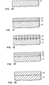
- FIGS. 1 to 4 show different stages of a conventional manufacturing process for bipolar transistors.
- Various process steps such as B. thermal oxidation, masking and etching, which are generally known, are not shown in the sequence of the process steps in Figures 1 to 4.
- the semiconductor die 11 has a thermal diffusion of an N-conducting interference element therein, such as, for. B. phosphorus, arsenic, antimony or the like.
- N-conducting interference element such as, for. B. phosphorus, arsenic, antimony or the like.
- Manufactured N + - conductive zone 13 is produced through an opening in an oxide layer according to customary process steps.
- arsenic is preferred in the formation of zone 13, which is then to serve as a buried sub-collector zone of the NPN transistor.
- concentration C of arsenic is preferably more than 10 tome 21 A / cm 3.
- An epitaxial layer 15 is formed on the surface of the semiconductor die 11.
- the N + - conducting zone 13 diffuses into the epitaxial layer 15, as shown in FIG. 1.
- P-type zones 17 and 19 are diffused into the surface of the semiconductor die 11 before the epitaxial layer 15 is formed.
- the P + conductive zones are used for insulation.
- the P + - conducting zones 17 and 19 also diffuse out.
- the P + -conducting zones 17 and 19 are formed by conventional diffusion methods, boron being preferably used as the interference element, although other P + -conducting interference elements can also be used.
- the initial concentration of boron, C o is preferably> 10 20 atoms / cm 3 .
- buried oxide insulation zones 21, 23 and 25 are formed in the epitaxial layer 15.
- a method for forming such buried oxide isolation zones in monocrystalline silicon is described in applicant's U.S. Patent No. 4,044,454.
- those surfaces of the semiconductor chips on which no buried oxide isolation zones are formed are covered by an insulating material, such as, for example, B. silicon nitride covered.
- openings are made at those locations of the silicon nitride layer where recessed oxide isolation zones are to be formed.
- the exposed monocrystalline zones are then first etched and then thermally oxidized so that the oxidation extends as far as the P + -conducting zones 17 and 19 and after the N + -conducting sub-collector zone 13.
- the initial concentration C o of the N + - type impurity element is preferably Tomen> 10 20 A / cm 3.
- a P + - conducting base zone 27 is then suitably formed in the surface of the epitaxial layer 15, such as e.g. B. formed by diffusion or ion implantation.
- the diffusion is preferably carried out with boron tribate with an initial surface concentration of 4 ⁇ 10 19 atoms / cm 3 . This concentration is then reduced by reoxidation in the base zone.
- the base can also be carried out with an ion implantation through an oxide layer, where C 0 is approximately 10 18 atoms / cm 3 . If the sub-collector zone 13 has diffused so far that it comes into contact with the base zone 27, then this intersection of two very heavily doped junctions results in one low breakdown voltage.
- part of the N-type epitaxial layer will be placed between the P + - base region 27 and the N + sub-collector region 13.
- the promotion of the diffusion of the sub-collector zone for this purpose is described in the applicant's US Pat. No. 4,016,596.
- a silicon dioxide layer 31 and a silicon nitride layer 33 are then deposited on the surface of the epitaxial layer in a conventional manner.
- An opening 35 and openings 37 and 39 are then produced in the silicon nitride layer 33 through the silicon nitride layer 33 and the silicon dioxide layer 31.
- a photoresist 41 is then applied to mask the opening 35, but leaves the openings 37 and 39 free for implantation of N t- doping ions to form the emitter zone 42 and the collector contact zone 39.
- Ion bombardment or ion implantation is preferably used today to produce emitter zones within a P-conducting base zone.
- an ion implantation runs at an energy level of approximately 50 KeV and a dose of approximately 1 x 10 16 Tomen for implanting a maximum concentration of about 10 21 to about 5 x 10 21 A / cm 3 + type in the surface of the P base region 27 from.
- the original ion bombardment implants the deepest penetration ions to a depth of about 30 nm to about 40 nm.
- the diffusion caused by tempering has the consequence that the emitter zone extends to a depth of about 300 to about 500 nm extends. If one wants to remove most of the structural defects that have occurred in this way by tempering, it is usually not possible to achieve an emitter depth of less than 200 nm after the tempering using ion implantation in the epitaxial surface layer. Since stray capacitance is created between the transition from the P + base region to the emitter region, it is desirable to limit the depth of the emitter region and to limit the extent of the transition between the side surface of the emitter region and the base region.
- FIGS. 5 to 10 the method according to the invention for producing a transistor structure is to be described.
- Figs. 5 to 8 process steps in the manufacture of a transistor structure, which are the same as those previously with reference to FIGS. 1 to 4 process steps described. The same parts are therefore used with the same but deleted reference numerals.
- the silicon dioxide layer 31 'and the silicon nitride layer 33' are deposited as shown in Fig. 8 and then openings 35 ', 37' and 39 'are made.
- a layer 43 of non-monocrystalline silicon (sometimes referred to as polysilicon) is then deposited on the surface of the transistor structure. As can be seen in FIG. 8, the layer of polycrystalline silicon fills the openings 35 ', 37' and 39 '. It is obvious, of course, that the figures in FIGS. 8 and 9 structure is greatly exaggerated in their proportions.
- the silicon dioxide layer is generally between 40 and 80 nm thick
- the silicon nitride layer 33 generally has a thickness of approximately 100 to approximately 200 nm.
- the polysilicon layer generally has a thickness of 50 to 150 nm.
- the depressions over the regions of the openings 35, 37 and 39 are of little importance.
- this polycrystalline layer is subjected to an ion implantation in the areas in the vicinity of the opening 37 ', which is to be regarded as a precursor which later forms the emitter zone of the bipolar transistor. It is not necessary to provide the transistor structure with a mask during the ion implantation, since other areas outside the openings 37 'and 39' are covered by a layer of SiO 2 or a layer sequence of SiO 2 / Si 3 N 4 . It is only necessary that the ion implantation proceed over the surface of the opening 37. The transistor structure is then left on for such a long time that the implanted ions are driven deeper into the base zone below the opening 37 and the polycrystalline silicon is converted into monocrystalline silicon.
- the method according to the present invention is best understood with reference to Figs. 10 to 14 and the diagram of FIG. 15.
- the originally monocrystalline silicon of the epitaxial layer 15 is shown in FIG. 10.
- the original silicon layer 15 for Explanation of the method according to the invention is shown as practically undoped, so in practice the epitaxial layer 15 would have different zones and areas of different conduction types and concentrations, e.g. B.
- a layer 43 of polysilicon is deposited on the epitaxial layer 15 made of monocrystalline silicon.
- the polycrystalline silicon can either be carried out by conventional low-pressure processes with chemical precipitation from the vapor phase at temperatures of the order of 650 ° C., the silicon vapor being derived from sources such as silane or silicon tetrachloride.
- a layer of polycrystalline silicon can also be applied by conventional evaporation methods, as described, for example, by C. Canali et al., In the Journal of Applied Physics Volume 46, No. 7, July 1975, pages 2831-2835, with the exception that the silicon is applied directly to the silicon substrate or by precipitation with sputtering.
- the layer thickness of the polycrystalline layer 43 is approximately 80 nm.
- the polycrystalline silicon is deposited directly as layer 43 on a monocrystalline silicon substrate, but that, as expected, silicon dioxide is formed during these process steps.
- this silicon dioxide layer has at most a thickness of the order of 0.5 to 2 nm and occupies a different continuity, for the sake of simplicity of illustration this silicon dioxide layer is indicated as layer 45 in FIG. 11.
- the bombardment can be carried out using conventional ion implantation devices at an energy level and a dosage that is sufficient to shift the Gaussian distribution of the bombarding ions over the interface between the polycrystalline layer 43 and the monocrystalline epitaxial layer 15, specifically into the P + - conducting base zone 27. This requirement is best seen in connection with FIG. 15.
- the concentration gradient of the ions resulting from the ion implantation forms a Gaussian distribution curve. At different energy levels and dosages, the concentration gradient lies entirely within the polycrystalline layer, as shown by the solid line in FIG. 15.
- the Gaussian distribution is completely within the polycrystalline layer, then a subsequent annealing process will not convert the polycrystalline silicon of the layer into the monocrystalline state. However, if the dosage exceeds a predetermined threshold for the particular ion to be implanted and the energy levels are high enough to shift the Gaussian distribution across the interface between the polycrystalline layer and the monocrystalline layer, then a subsequent tempering process will cause the polysilicon layer to be in one converts a monocrystalline state.
- ion bombardment at room temperature and an energy level of 50 to 200 KeV and a dosage of at least 10 16 ions / cm 2 is sufficient to shift the Gaussian distribution across the interface between the polycrystalline layer and the monocrystalline layer. If it is desired to use a lower dosage of the doping ions, then the ion bombardment can be carried out in two stages in such a way that first a doping ion is used in the first stage and a non-doping ion such as e.g. . As silicon or hydrogen.
- the two-step process Ren can also be used to form P t -containing emitter zones if the dosage of the implantation of P + - -containing doping ions is below the threshold level and / or the energy level is not sufficient to shift the Gaussian distribution across the interface.
- FIGS. 13 and 14 subject the transistor structure to a start cycle where the implanted ions are electrically activated by suitable treatment. Threshold metering is required to make polysilicon amorphous. Amorphous polysilicon is required for later recrystallization. Since the implanted ions break up the oxide at the interface, the recrystallization takes place at relatively low temperatures. This is actually a solid state process with epitaxial growth. If the dosage is not sufficient to break up the oxide present on the separating surface, then recrystallization cannot take place even at very high temperatures.
- an epitaxial layer 43 consisting of monocrystalline silicon grows through consumption of the now amorphous polycrystalline silicon layer 43, which is actually converted into monocrystalline silicon during this heat cycle.
- the dashed zone 45 in FIGS. 13 and 14 all the silicon dioxide that was present as layer 45 on the separating surface has in fact disappeared and therefore does not interfere with the formation of the epitaxial layer 43 ′ consisting of monocrystalline silicon.
- the annealing can be done by laser beams, electron beams or by conventional heat treatment such as. B. heating the transistor structure.
- Heat treatment by thermal tempering can be accomplished by any time / temperature cycle that is related to tempering and thus suitable for eliminating faults on the interface in the usual way.
- a two-stage process is preferred for the preferred heat cycle for tempering, the temperature being initially kept at 550 ° C. for two hours in a first stage, while the temperature is then raised to 900 ° C., and the transistor structure for one hour is kept at 900 ° C.
- the transistor structure is held at a temperature of about 800 ° C to about 1000 ° C for about 30 minutes to about 4 hours.
- the highest temperature in the tempering cycle should not be higher than 1000 ° C to keep out diffusion small.
- the silicon layer 43 need not be completely converted to the monocrystalline silicon layer 43'.
- the structure can be subjected to a usual thermal oxidation in situ for a short time sufficient to convert the remaining amorphous silicon of the layer to silicon dioxide.
- This silicon dioxide layer can then be selective are removed from the surface of the structure using an etchant, such as buffered hydrofluoric acid, which selectively etches off the silicon dioxide thus formed and thereby exposes the surface of the monocrystalline epitaxial layer 43 'formed.
- the monocrystalline, epitaxial layer 43 ′ thus formed is selectively removed and thus forms an emitter zone 47 and a collector contact 49.
- the subsequent formation of ohmic contacts and metallizations (not shown) for the individual semiconductor devices can be done in the usual way.
- the possibility of a short circuit from the emitter contact to the base zone is eliminated by the fact that there is a vertical distance between the base zone and the emitter zone. This elimination of the short circuit problems is maintained even with very flat emitter structures.
- Another property of this transistor constructed and manufactured according to the invention is that the gain of the transistor has been improved by approximately 50 to 65% compared to previously known transistor structures. The reason for this significant and surprising improvement in the operational behavior of the transistor is not known. It is obvious that the combination of improved performance and simpler manufacture are new and unique properties of the transistor constructed and manufactured according to the invention.
Landscapes
- Bipolar Transistors (AREA)
Abstract
Description
- Die Erfindung betrifft ein Verfahren zum Herstellen eines Transistors und insbesondere zum Herstellen eines Transistors mit einer neuartigen Emitterstruktur und einer höheren Verstärkung.
- Transistorstrukturen sind allgemein bekannt. Normalerweise wird für die Herstellung eines NPN-Transistors eine hochdotierte N+-leitende Subkollektorzone in die Hauptfläche eines Halbleitersubstrats eindiffundiert. Dann wird über der Oberfläche des Substrats eine epitaxiale Schicht aufgewachsen. Die Subkollektorzone dringt dabei während des Niederschlagens der epitaxialen Schicht durch Ausdiffusion in diese ein. Anschließend wird eine Basiszone durch Eindiffundieren eines P-leitenden Störelementes in die epitaxiale Schicht in Berührung mit der Subkollektorzone gebildet. Dann wird ein N-leitendes Störelement, wie z. B. Arsen oder Phosphor, zur Bildung der Emitterzone des Transistors in die Basiszone eindiffundiert. Die Emitterzone liegt damit vollständig unterhalb der Oberfläche und innerhalb der Basiszone der epitaxialen Schicht.
- Das dabei wegen seiner Wirtschaftlichkeit und seinen besseren Steuerungsmöglichkeiten bevorzugte Verfahren besteht darin, daß das zur Bildung der Emitterzone einzudiffundierende Störelement durch Ionenimplantation eingebracht wird. Es kann jedoch nicht übersehen werden, daß die Verwendung von Ionenimplantation zur Bildung einer Emitterzone innerhalb der Basiszone einer epitaxial aufgewachsenen Schicht zu zahlreichen Schwierigkeiten geführt hat.
- Während der Ionenimplantation wird die monokristalline Struktur der epitaxialen Schicht aufgrund der Strahlungsschäden stark beeinträchtigt, wenn nicht gar zerstört. Nach Beendigung des Ionenbeschusses muß die kristalline Struktur dadurch wiederhergestellt werden, daß das Material einer Wärmebehandlung zum Anlassen unterzogen wird. Obgleich diese Wärmebehandlung zum Anlassen ausreicht, den größten Teil der zerstörten kristallinen Struktur wieder herzustellen, bleiben doch einige Restschäden der Struktur übrig. Diese kristallinen Defekte können aber das Betriebsverhalten des Transistors beeinträchtigen. Außerdem bewirkt die zum Anlassen durchgeführte Wärmebehandlung, daß die implantierten, dotierenden Ionen weiter in die Basiszone eindringen. Das Eintreiben implantierter, dotierender Ionen hat zur Folge, daß die Tiefe der Emitterzone größer wird, als erwünscht. Außerdem liefert die Nachbarschaft der Seitenflächen der Emitterzone zusammen mit der diesen Seitenflächen der Emitterzone benachbarten Teilen der Basiszone eine Streukapazität, die höher ist, als erwünscht.
- Eine weitere Schwierigkeit besteht darin, daß die nachfolgende Metallisierung der Emitterzone auf der Oberfläche der epitaxialen Schicht stattfindet. Üblicherweise wird dabei auf der Siliziumoberfläche über der Emitterzone Platin niedergeschlagen. Durch nachfolgende Behandlung erhält man auf der Oberfläche Platinsilicid. Das zur Bildung des Platinsilicids nötige Silicium wird jedoch dem Silicium der epitaxial aufgewachsenen Schicht entnommen, und dabei tritt auch noch ein seitliches Wachstum der Platinsilicidschicht auf. Ein solches seitliches Wachstum kann jedoch einen Kurzschluß zwischen Emitterzone und Basiszone an der Oberfläche zur Folge haben. Wegen der außerordentlich geringen Zwischenräume, die bei der Bildung von Transistoren üblich sind, ist die Möglichkeit eines derartigen Kurzschlusses zwischen Emitter und Basis durchaus gegeben und stellt ein ständig auftretendes Problem dar.
- Es wäre daher erwünscht, einen Transistor zu schaffen, bei dem der Kontakt zwischen Seitenfläche der Basiszone und Emitter soweit verringert wird, daß dadurch auch die Streukapazität zwischen Emitter- und Basiszone verringert wird. Es wäre außerdem wünschenswert, wenn man eine Transistorstruktur hätte, bei der die Emitterzone flacher ist, wobei mindestens ein Teil der Emitterzone von der Basiszone isoliert ist. Ein Transistor mit einer kleineren Emitterzone kann viel schneller vom leitenden in den nichtleitenden Zustand und umgekehrt, umschalten. Es wäre außerdem erwünscht, wenn man eine Emitterstruktur hätte, bei der die Metallisierung an einem Ort stattfindet, wo nicht die Gefahr einer Kontaktbrücke besteht.
- Gemäß der vorliegenden Erfindung wird ein Transistor geschaffen, dessen Emitter aus nicht-monokristallinem Silicium gebildet wird, das während der Herstellung des Transistors in monokristallines Silicium umgewandelt wird. Bei dem Verfahren zum Herstellen dieser Transistorstruktur wird eine Subkollektorzone in einem Halbleitersubstrat gebildet. Der in der Subkollektorzone vorhandene Dotierungsstoff diffundiert durch Ausdiffusion in eine nachträglich niedergeschlagene epitaxiale Schicht hinein. In dieser epitaxialen Schicht wird eine Basiszone gebildet, deren Leitungstyp dem Leitungstyp der Subkollektorzone entgegengesetzt ist. Dadurch erhält man einen PN-Ubergang zwischen der Basiszone und den aus der Subkollektorzone ausdiffundierten Störelementen, die die Kollektorzone des Transistors bilden.
- Auf der epitaxialen Schicht wird dann eine Schicht aus nicht-monokristallinem Silicium niedergeschlagen. Mindestens ein Teil dieser nicht-monokristallinen Siliciumschicht bildet einen Vorläufer für eine Emitterzone, die mit einem Abstand in vertikaler Richtung von der Oberfläche der Basiszone dieser gegenüberliegt. Der Vorläufer für die Emitterzone wird dann mit Ionen bombardiert, die den gleichen Leitungstyp ergeben, wie ihn die Subkollektorzone aufweist. Die Ionenbombardierung wird mit einer Dosierung und einem Energieniveau durchgeführt, das ausreicht, ein Teil der Gauss'schen Verteilung der Ionen über der Trennfläche zwischen der monokristallinen Schicht und der epitaxialen Schicht in die Basiszone hineinzuverlagern. Danach wird die Gesamtstruktur in geeigneter Weise angelassen, so daß ein Teil der Ionen tiefer in die Basiszone eingetrieben wird und das nicht-monokristalline Silizium des Vorläufers der Emitterzone in eine Emitterzone aus monokristallinem Silicium umgewandelt wird.
- Die sich dabei ergebende Struktur hat den Vorzug, daß die Gesamttiefe der Emitterzone kleiner ist als bei einer durch unmittelbare Bombardierung der epitaxialen Schicht mit Ionen gebildeten Emitterzone. Außerdem ist der seitliche Kontakt zwischen Emitterzone und Basiszone stark verringert und die unerwünschte Streukapazität von Emitterzone nach Basiszone ist wesentlich herabgesetzt. Ein weiterer wesentlicher Vorteil der Erfindung liegt darin, daß die Emitterzone an einer Stelle metallisiert werden kann, die von der Oberfläche der epitaxialen Schicht einen Abstand aufweist, so daß dadurch die Gefahr des Eindringens von Metall vermieden wird. Ein weiterer unerwarteter Vorteil der Erfindung besteht darin, daß der erfindungsgemäß hergestellte Transistor im Vergleich mit Transistoren des Standes der Technik eine wesentlich bessere Verstärkung aufweist.
- Die Erfindung wird nunmehr anhand eines Ausführungsbeispiels in Verbindung mit den beigefügten Zeichnungen im einzelnen näher erläutert.
- In den Zeichnungen zeigen:
- Fign. 1 bis 4 verschiedene Stufen bei der Herstellung eines Halbleitertransistors gemäß einem bekannten Verfahren,
- Fign. 5 bis 9 verschiedene Stufen bei der Herstellung eines Halbleitertransistors nach dem erfindungsgemäßen Verfahren,
- Fign. 10 bis 14 vergrößerte Ansichten der epitaxialen Oberflächenschicht, der Polysiliciumschicht und der Trennfläche während der Herstellung einer Emitterzone nach dem erfindungsgemäßen Verfahren und
- Fig. 15 eine schematische Darstellung der Gauss' schen Verteilung der Ionen in der nicht-monokristallinen Schicht und in der epitaxial aufgewachsenen Schicht.
- Für die bevorzugte Ausführungsform der Erfindung wird ein P-leitendes Siliciumsubstrat zur Bildung eines bipolaren NPN-Transistors verwendet. Selbstverständlich ist die Erfindung genauso auf die Herstellung eines bipolaren Transistors entgegengesetzter Leitfähigkeit und auf andere Arten von Halbleitervorrichtungen anwendbar. Dieses Verfahren läßt sich nämlich genauso gut für die Bildung eines N-leitenden Kanals oder eines Pleitenden Kanals bei Feldeffekttransistoren einsetzen. Es ergeben sich jedoch bei der Anwendung der Erfindung auf Feldeffekttransistoren keine Verbesserungen der Betriebseigenschaften, jedoch läßt sich das Verfahren leicht dahin abwandeln, daß Feldeffekttransistoren während der gleichzeitigen Herstellung von bipolaren Transistoren ebenso leicht gefertigt werden können.
- In den Figuren 1 bis 4 sind verschiedene Stufen eines üblichen Herstellungsverfahren für bipolare Transistoren gezeigt. Verschiedene Verfahrensschritte, wie z. B. thermische Oxidation, Maskieren und Ätzen, die allgemein bekannt sind, sind in der Folge der Verfahrensschritte in den Figuren 1 bis 4 nicht besonders gezeigt. Wie aus Figur 4 zu erkennen, weist das Halbleiterplättchen 11 eine darin liegende, durch thermische Diffusion eines N-leitenden Störelements, wie z. B. Phosphor, Arsen, Antimon oder dgl. hergestellte N+- leitende Zone 13 auf. Die N+-leitende Zone 13 wird durch eine Öffnung in einer Oxidschicht nach üblichen Verfahrensschritten hergestellt. Aus dem Fachmann bekannten Gründen ist Arsen bei der Bildung der Zone 13 vorzuziehen, die anschließend als vergrabene Subkollektorzone des NPN-Transistors dienen soll. Zu Beginn beträgt die Konzentration C von Arsen vorzugsweise mehr als 1021 Atome/cm3.
- Auf der Oberfläche des Halbleiterplättchens 11 wird eine epitaxiale Schicht 15 gebildet. Während der Bildung der epitaxialen Schicht 15 diffundiert die N+-leitende Zone 13 in die epitaxiale Schicht 15 hinein, wie dies Fig. 1 zeigt. Außerdem werden P-leitende Zonen 17 und 19 vor Bildung der Epitaxialschicht 15 in die Oberfläche des Halbleiterplättchens 11 eindiffundiert. Die P+-leitenden Zonen dienen der Isolation. Während der Bildung der epitaxialen Schicht 15 diffundieren die P+-leitenden Zonen 17 und 19 ebenfalls aus. Die P+-leitenden Zonen 17 und 19 werden durch übliche Diffusionsverfahren gebildet, wobei als Störelement vorzugsweise Bor verwendet wird, obwohl auch andere P+-leitende Störelemente verwendbar sind. Die anfängliche Konzentration des Bors, Co, liegt vorzugsweise bei > 1020 Atomen/cm3.
- Wie man anschließend am besten aus Figur 2 erkennt, werden versenkte Oxidisolationszonen 21, 23 und 25 in der epitaxialen Schicht 15 gebildet. Ein Verfahren zur Bildung solcher versenkter Oxidisolationszonen in monokristallinem Silicium ist in der US-Patentschrift Nr. 4 044 454 der Anmelderin beschrieben. Bei diesem Verfahren werden diejenigen Oberflächen der Halbleiterplättchen, bei denen keine versenkten Oxidisolationszonen gebildet werden, durch ein isolierendes Material, wie z. B. Siliciumnitrid abgedeckt. Dann werden an denjenigen Stellen der Siliciumnitridschicht, an denen eingelassene Oxidisolationszonen gebildet werden sollen, Öffnungen hergestellt. Die freiliegenden monokristallinen Zonen werden dann zunächst geätzt und dann thermisch durchoxidiert, so daß die Oxidation bis nach der P+-leitenden Zonen 17 und 19 und nach der N+-leitenden Subkollektorzone 13 reichen.
- Nach Bildung der eingelassenen Oxidationszonen werden selektiv Diffusionen in die Epitaxialschicht 15 zur Bildung einer N+-leitenden Zone 29 hergestellt. Diese Zone 29 dient dann als Kollektorkontakt. Die anfängliche Konzentration Co des N+-leitenden Störelements, vorzugsweise Arsen, liegt vorzugsweise bei > 1020 Atomen/cm3.
- Dann wird in der Oberfläche der epitaxialen Schicht 15 eine P+-leitende Basiszone 27 in geeigneter Weise, wie z. B. durch Diffusion oder Ionenimplantation gebildet. Die Diffusion wird dabei vorzugsweise mit Bortriborat mit einer Anfangsoberflächenkonzentration von 4 x 10¹⁹ Atomen/cm3 vorgenommen. Diese Konzentration wird anschließend durch Reoxidation in der Basiszone verringert. Die Basis kann außerdem mit einer Ionenimplantation durch eine Oxidschicht durchgeführt werden, wobei C0 annähernd 1018 Atome/cm3 beträgt. Wenn die Subkollektorzone 13 so weit ausdiffundiert hat, daß sie in Kontakt mit der Basiszone 27 kommt, dann ergibt dieser Schnitt zweier sehr stark dotierter Übergänge eine niedrige Durchschlagsspannung. Wenn jedoch eine höhere Durchschlagsspannung gewünscht wird, dann wird man einen Teil der N-leitenden epitaxialen Schicht zwischen die P+-leitende Basiszone 27 und die N+leitende Subkollektorzone 13 legen. Die Förderung der Ausdiffusion der Subkollektorzone zu diesem Zweck ist in der der Anmelderin gehörenden US-Patentschrift 4 016 596 beschrieben.
- Wie aus Fig. 4 zu ersehen, werden dann eine Siliciumdioxidschicht 31 und eine Siliciumnitridschicht 33 auf der Oberfläche der epitaxialen Schicht auf übliche Weise niedergeschlagen. Anschließend wird in der Siliciumnitridschicht 33 eine Öffnung 35 und öffnungen 37 und 39 durch die Siliciumnitridschicht 33 und die Siliciumdioxidschicht 31 hergestellt. Anschließend wird ein Photolack 41 zur Maskierung der Öffnung 35 aufgebracht, der jedoch die öffnungen 37 und 39 für eine Implantation von Nt-dotierenden Ionen zur Bildung der Emitterzone 42 und der Kollektorkontaktzone 39 freiläßt.
- Zur Herstellung von Emitterzonen innerhalb einer P-leitenden Basiszone wird heute bevorzugt Ionenbombardierung oder Ionenimplantation verwendet. Im allgemeinen läuft eine Ionenimplantation bei einem Energieniveau von annähernd 50 KeV und einer Dosierung von annähernd 1 x 10¹⁶ für die Implantierung einer maximalen Konzentration von etwa 1021 bis etwa 5 x 10²¹ Atomen/cm3 in die Oberfläche der P+-leitenden Basiszone 27 ab. Während der Ionenimplantation der monokristallinen Struktur der epitaxialen Schicht wird diese aufgerissen und erleidet starke Strukturschäden. Diese Strukturschäden werden mindestens zum Teil durch Anlassen der Transistorstruktur bei einer Temperatur von 900 bis 1000 C für eine Dauer von etwa 30 bis 60 Minuten geheilt. Obgleich dieses Anlaßverfahren die meisten durch die implantierten Ionen verursachten Störungen der Kristallstruktur beseitigt und die meisten implantierten Ionen elektrisch wieder aktiviert, so gibt es doch immer noch eine merkliche Anzahl von Dislozierungen in der Emitterstruktur und diese neigen dazu, das Betriebsverhalten zu beeinträchtigen. Außerdem wird durch das Anlaßverfahren die Ausdiffusion der N+-leitenden Ionen bewirkt, so daß sich die Emitterzone, von der Oberfläche der Epitaxialschicht aus gesehen, ausdehnt.
- Allgemein gesprochen, bewirkt die ursprüngliche Ionenbombardierung eine Implantation der am tiefsten eindringenden Ionen bis zu einer Tiefe von etwa 30 nm bis etwa 40 nm. Die durch Anlassen bewirkte Ausdiffusion hat zur Folge, daß sich die Emitterzone bis zu einer Tiefe von etwa 300 bis etwa 500 nm ausdehnt. Will man die meisten der so aufgetretenen Strukturdefekte durch Anlassen beseitigen, so ist es gewöhnlich nicht möglich, nach dem Anlassen unter Verwendung von Ionenimplantation in die epitaxiale Oberflächenschicht eine Emittertiefe von weniger als 200 nm zu erzielen. Da eine Streukapazität zwischen dem Übergang von der P+-leitenden Basiszone nach der Emitterzone hervorgerufen wird, ist es erwünscht, die Tiefe der Emitterzone zu beschränken sowie das Ausmaß des Übergangs zwischen der Seitenfläche der Emitterzone und der Basiszone einzuschränken.
- In Zusammenhang mit den Fign. 5 bis 10 soll das erfindungsgemäße Verfahren zum Herstellen einer Transistorstruktur beschrieben werden. Im allgemeinen zeigen Fign. 5 bis 8 Verfahrensstufen bei der Herstellung einer Transistorstruktur, die die gleichen sind, wie die zuvor in bezug auf Fign. 1 bis 4 beschriebenen Verfahrensstufen. Gleiche Teile sind daher mit gleichen, aber gestrichenen Bezugszeichen verwendet.
- Die Siliciumdioxidschicht 31' und die Siliciumnitridschicht 33' werden, wie in Fig. 8 gezeigt, niedergeschlagen und anschließend werden Öffnungen 35', 37' und 39' hergestellt. Eine Schicht 43 aus nicht-monokristallinem Silicium (das manchmal auch als Polysilicium bezeichnet wird), wird dann auf der Oberfläche der Transistorstruktur niedergeschlagen. Wie in Fig. 8 zu erkennen, füllt die Schicht aus polykristallinem Silicium die öffnungen 35', 37' und 39' aus. Es ist selbstverständlich einleuchtend, daß die in Fign. 8 und 9 dargestellte Struktur in ihren Größenverhältnissen stark übertrieben ist. Die Siliciumdioxidschicht ist im allgemeinen zwischen 40 und 80 nm stark, die Siliciumnitridschicht 33 hat im allgemeinen eine Dicke von etwa 100 bis etwa 200 nm. Die Polysiliciumschicht hat im allgemeinen eine Dicke von 50 bis 150 nm. Die Vertiefungen über den Bereichen der öffnungen 35, 37 und 39 sind jedoch ohne große Bedeutung.
- Nach Niederschlagen der polykristallinen Schicht 43 wird diese polykristalline Schicht einer Ionenimplantation in den Bereichen in der Nachbarschaft der öffnung 37' unterzogen, die als Vorläufer zu betrachten ist, der später die Emitterzone des bipolaren Transistors bildet. Es ist dabei nicht erforderlich, während der Ionenimplantation die Transistorstruktur mit einer Maske zu versehen, da andere Bereiche außerhalb der Öffnungen 37' und 39' durch eine Schicht aus Si02 oder eine Schichtenfolge aus Si02/Si3N4 überdeckt sind. Es ist nur erforderlich, daß die Ionenimplantation über der Oberfläche der Öffnung 37 vor sich geht. Danach wird die Transistorstruktur für eine so lange Zeit angelassen, daß die implantierten Ionen tiefer in die Basiszone unterhalb der öffnung 37 eingetrieben werden und das polykristalline Silicium in monokristallines Silicium umgewandelt wird.
- Das Verfahren gemäß der vorliegenden Erfindung ist wohl am besten verständlich, im bezug auf die Fign. 10 bis 14 und das Diagramm der Fig. 15. Das ursprünglich monokristalline Silicium der epitaxialen Schicht 15, ist in Fig. 10 dargestellt. Obgleich die ursprüngliche Siliciumschicht 15 zur Erläuterung des erfindungsgemäßen Verfahrens als praktisch undotiert dargestellt ist, so würde doch in der Praxis die epitaxiale Schicht 15 verschiedene Zonen und Bereiche unterschiedlicher Leitungstypen und Konzentrationen aufweisen, wie z. B. die P+-leitende Basiszone 27. In Fig. 11 wird auf der epitaxialen Schicht 15 aus monokristallinem Silicium eine Schicht 43 aus Polysilicium niedergeschlagen. Das polykristalline Silicium kann dabei entweder durch übliche Niederdruckverfahren mit chemischem Niederschlag aus der Dampfphase bei Temperaturen in der Größenordnung von 650 C durchgeführt werden, wobei der Siliciumdampf aus Quellen, wie Silan oder Siliciumtetrachlorid, abgeleitet wird. Andererseits kann auch eine Schicht aus polykristallinem Silicium durch übliche Verdampfungsverfahren aufgebracht werden, wie sie beispielsweise durch C. Canali et al., im Journal of Applied Physics Band 46, Nr. 7, Juli 1975 auf Seiten 2831 - 2835 beschrieben werden, mit der Ausnahme, daß das Silicium unmittelbar auf das Siliciumsubstrat oder durch Niederschlag mit Kathodenzerstäubung aufgebracht wird. Für'die vorliegende Darstellung beträgt die Schichtdicke der polykristallinen Schicht 43 etwa 80 nm.
- Es sei darauf hingewiesen, daß zwar das polykristalline Silicium als Schicht 43 unmittelbar auf einem monokristallinem Siliciumsubstrat niedergeschlagen wird, daß sich dabei aber erwartungsgemäß während dieser Verfahrensschritte Siliciumdioxid bildet. Obgleich diese Siliciumdioxidschicht höchstens eine Dicke in der Größenordnung von 0,5 bis 2 nm aufweist und eine unterschiedliche Kontinuität besetzt, so ist doch der Einfachheit der Darstellung halber diese Siliciumdioxidschicht in Fig. 11 als Schicht 45 angedeutet.
- Als nächstes wird gemäß Fig. 12 das Substrat einer Ionenimplantation mit einem dotierenden Ion, wie z. B. Arsen, ausgesetzt. Die Bombardierung kann dabei unter Verwendung üblicher Ionenimplantationsvorrichtungen bei einem Energieniveau und einer Dosierung durchgeführt werden, die ausreicht, die Gauss'sche Verteilung der bombardierenden Ionen über der Trennfläche zwischen der polykristallinen Schicht 43 und der monokristallinen epitaxialen Schicht 15 zu verschieben und zwar in die P+-leitende Basiszone 27 hinein. Dieses Erfordernis ist am besten im Zusammenhang mit Fig. 15 zu sehen. Wie aus Fig. 15 zu erkennen ist, bildet der Konzentrationsgradient der sich aus der Ionenimplantation ergebenden Ionen eine Gauss'sche Verteilungskurve. Bei verschiedenen Energieniveaus und Dosierungen liegt der Konzentrationsgradient vollständig innerhalb der polykristallinen Schicht, wie dies durch die ausgezogene Linie in Fig. 15 dargestellt ist. Wenn die Gauss'sche Verteilung vollständig innerhalb der polykristallinen Schicht liegt, dann wird ein nachfolgender Anlaßvorgang das polykristalline Silicium der Schicht nicht in den monokristallinen Zustand umsetzen. Wenn jedoch die Dosierung einen vorbestimmten Schwellwert für das bestimmte zu implantierende Ion überschreitet und die Energieniveaus ausreichend hoch sind um die Gauss'sche Verteilung über die Trennfläche zwischen polykristalliner Schicht und monokristalliner Schicht zu verschieben, dann wird ein nachfolgender Anlaßvorgang bewirken, daß die Polysiliciumschicht sich in einen monokristallinen Zustand umwandelt.
- Unter Verwendung von Arsenionen reicht ein Ionenbombardement bei Zimmertemperatur und einem Energieniveau von 50 bis 200 KeV und einer Dosierung von mindestens 1016 Ionen/cm2 aus, um die Gauss' sche Verteilung über die Trennfläche zwischen polykristalliner Schicht und monokristalliner Schicht zu verschieben. Sollte es erwünscht sein, eine geringere Dosierung der dotierenden Ionen zu verwenden, dann kann die Ionenbombardierung in zwei Stufen in der Weise durchgeführt werden, daß zunächst in der ersten Stufe ein dotierendes Ion verwendet wird und in der zweiten Stufe ein nicht dotierendes Ion, wie z. B. Silicium oder Wasserstoff. Das Zwei-Stufen-Verfahren kann außerdem zur Bildung von Pt-leitenden Emitterzonen eingesetzt werden, wenn die Dosierung der Implantation von P+-leitenden Dotierungsionen unterhalb des Schwellwertpegels liegt, und/oder das Energieniveau nicht ausreicht, die Gauss'sche Verteilung über die Trennfläche zu verschieben.
- Dann wird gemäß Fign. 13 und 14 die Transistorstruktur einem Anlaßzyklus unterworfen, wo durch geeignete Behandlung die implantierten Ionen elektrisch aktiviert werden. Die Schwellwertdosierung ist erforderlich, um Polysilicium amorph zu machen. Für eine spätere Rekristallisierung ist amorphes Polysilicium erforderlich. Da die implantierten Ionen das Oxid an der Trennfläche aufbrechen, läuft die Rekristallisierung bei relativ niedrigen Temperaturen ab. Dies ist tatsächlich ein im festen Zustand ablaufendes Verfahren mit epitaxialem Wachstum. Reicht die Dosierung nicht aus, um das an der Trennfläche vorhandene Oxid aufzubrechen, dann kann selbst bei sehr hohen Temperaturen keine Rekristallisation stattfinden. Während des Anlaßzyklus wächst, von der Trennfläche mit der monokristallinen epitaxialen Schicht 15 ausgehend, eine aus monokristallinem Silicium bestehende epitaxiale Schicht 43 durch Verbrauch der nunmehr amorphen polykristallinen Siliciumschicht 43 auf, die während dieses Wärmezyklus tatsächlich in monokristallines Silicium umgewandelt wird. Wie durch die gestrichelte Zone 45 in den Fign. 13 und 14 angedeutet, ist tatsächlich alles Siliciumdioxid, das als Schicht 45 an der Trennfläche vorhanden war, verschwunden und stört daher die Bildung der aus monokristallinen Silicium bestehenden Epitaxialschicht 43' nicht.
- Das Anlassen kann durch Laserstrahlen, Elektronenstrahlen oder durch übliche Wärmebehandlung, wie z. B. Aufheizen der Transistorstruktur, durchgeführt werden. Die Wärmebehandlung durch thermisches Anlassen kann durch jeden beliebigen Zeit-/ Temperaturzyklus erreicht werden, der sich zum Anlassen und damit zum Beseitigen von Störungen an der Trennfläche in üblicher Weise eignet. Für das vorliegende Ausführungsbeispiel wird für den bevorzugten Wärmzyklus zum Anlassen ein zweistufiges Verfahren bevorzugt, wobei zunächst in einer ersten Stufe die Temperatur für zwei Stunden auf 550 °C gehalten wird, während anschließend die Temperatur auf 900 °C erhöht, und die Transistorstruktur für eine Stunde bei 900 °C gehalten wird. Bei einem einstufigen Wärmezyklus wird die Transistorstruktur für etwa 30 Minuten bis etwa 4 Stunden bei einer Temperatur von etwa 800 °C bis etwa 1000 °C gehalten. Für beste Ergebnisse sollte die höchste Temperatur im Anlaßzyklus nicht höher liegen, als 1000 °C, um jede Ausdiffusion klein zu halten.
- Wie aus Fig. 14 zu erkennen, setzt sich die Umwandlung der polykristallinen Siliciumschicht 43 in eine monokristalline epitaxiale Schicht 43 solange fort, bis die Schicht 43 vollständig rekristallisiert ist und die sich dabei ergebende Struktur aus einer monokristallinen Siliciumschicht 43' über der monokristallinen, epitaxialen Schicht 15 besteht. Das allgemeine Verfahren zum Umwandeln nicht-monokristallinen Siliciums in monokristallines Silicium nach Bombardierung mit neutralen Ionen ist in der US-Patentschrift 3 900 445 offenbart.
- Es sei darauf hingewiesen, daß dann, wenn die niedergeschlagene polykristalline Siliciumschicht 43 geringfügig dicker ist, als für die endgültig zu bildende aus monokristallinem Silicium bestehende Epitaxialschicht 43' nötig ist, die Siliciumschicht 43 nicht vollständig in die monokristalline Siliciumschicht 43' umgewandelt werden muß. Zu einem geeigneten Zeitpunkt vor dem Ende der Umwandlung, kann die Struktur einer üblichen, thermischen Oxidation in situ für eine kurze Zeit ausgesetzt werden, die ausreicht, um das verbleibende amorphe Silicium der Schicht in Siliciumdioxid umzuwandeln. Diese Siliciumdioxidschicht kann dann anschließend selektiv von der Oberfläche der Struktur unter Verwendung eines Ätzmittels, wie beispielsweise gepufferter Flußsäure, entfernt werden, die selektiv das so gebildete Siliciumdioxid abätzt und damit die Oberfläche der gebildeten monokristallinen, epitaxialen Schicht 43' freilegt.
- Wie in Fig. 9 zu sehen, wird die so gebildete monokristalline, epitaxiale Schicht 43' selektiv entfernt und bildet damit eine Emitterzone 47 und einen Kollektorkontakt 49. Die nachfolgende Bildung von Ohm'schen Kontakten und Metallisierungen (nicht gezeigt) für die einzelnen Halbleitervorrichtungen kann auf übliche Weise vorgenommen werden. Es sei jedoch darauf verwiesen, daß die Möglichkeit eines Kurzschlusses vom Emitterkontakt nach der Basiszone dadurch beseitigt ist, daß zwischen Basiszone und Emitterzone ein Abstand in senkrechter Richtung besteht. Diese Beseitigung der Kurzschlußprobleme wird selbst bei sehr flachen Emitterstrukturen beibehalten.
- Eine weitere Eigenschaft dieses erfindungsgemäß aufgebauten und hergestellten Transistors besteht darin, daß die Verstärkung des Transistors gegenüber bisher bekannten Transistorstrukturen um etwa 50 bis 65 % verbessert worden ist. Der Grund für diese wesentliche und überraschende Verbesserung im Betriebsverhalten des Transistors ist nicht bekannt. Es ist offensichtlich, daß die Kombination aus verbesertem Betriebsverhalten und einfacherer Herstellung neue und einzigartige Eigenschaften des erfindungsgemäß aufgebauten und hergestellten Transistors sind.
Claims (6)
Applications Claiming Priority (2)
| Application Number | Priority Date | Filing Date | Title |
|---|---|---|---|
| US9366679A | 1979-11-13 | 1979-11-13 | |
| US93666 | 1979-11-13 |
Publications (3)
| Publication Number | Publication Date |
|---|---|
| EP0028739A2 true EP0028739A2 (de) | 1981-05-20 |
| EP0028739A3 EP0028739A3 (en) | 1982-06-23 |
| EP0028739B1 EP0028739B1 (de) | 1985-03-27 |
Family
ID=22240114
Family Applications (1)
| Application Number | Title | Priority Date | Filing Date |
|---|---|---|---|
| EP80106481A Expired EP0028739B1 (de) | 1979-11-13 | 1980-10-23 | Verfahren zum Bilden der Emitterzone eines Transistors |
Country Status (2)
| Country | Link |
|---|---|
| EP (1) | EP0028739B1 (de) |
| DE (1) | DE3070390D1 (de) |
Cited By (4)
| Publication number | Priority date | Publication date | Assignee | Title |
|---|---|---|---|---|
| DE3831555A1 (de) * | 1987-09-18 | 1989-04-06 | Toshiba Kawasaki Kk | Verfahren zum herstellen einer halbleitervorrichtung |
| US5116770A (en) * | 1988-07-14 | 1992-05-26 | Matsushita Electric Industrial Co., Ltd. | Method for fabricating bipolar semiconductor devices |
| US5236851A (en) * | 1988-07-14 | 1993-08-17 | Matsushita Electric Industrial Co., Ltd. | Method for fabricating semiconductor devices |
| US8318423B2 (en) | 2004-07-06 | 2012-11-27 | Focus Diagnostics, Inc. | Methods and compositions for detecting rhinoviruses |
Family Cites Families (6)
| Publication number | Priority date | Publication date | Assignee | Title |
|---|---|---|---|---|
| US3585088A (en) * | 1968-10-18 | 1971-06-15 | Ibm | Methods of producing single crystals on supporting substrates |
| US4109273A (en) * | 1974-08-16 | 1978-08-22 | Siemens Aktiengesellschaft | Contact electrode for semiconductor component |
| JPS51128268A (en) * | 1975-04-30 | 1976-11-09 | Sony Corp | Semiconductor unit |
| US4133704A (en) * | 1977-01-17 | 1979-01-09 | General Motors Corporation | Method of forming diodes by amorphous implantations and concurrent annealing, monocrystalline reconversion and oxide passivation in <100> N-type silicon |
| US4099987A (en) * | 1977-07-25 | 1978-07-11 | International Business Machines Corporation | Fabricating integrated circuits incorporating high-performance bipolar transistors |
| US4151420A (en) * | 1977-12-08 | 1979-04-24 | International Business Machines Corporation | Apparatus for the formation of epitaxial layers doped with conductivity-determining impurities by ion deposition |
-
1980
- 1980-10-23 DE DE8080106481T patent/DE3070390D1/de not_active Expired
- 1980-10-23 EP EP80106481A patent/EP0028739B1/de not_active Expired
Cited By (6)
| Publication number | Priority date | Publication date | Assignee | Title |
|---|---|---|---|---|
| DE3831555A1 (de) * | 1987-09-18 | 1989-04-06 | Toshiba Kawasaki Kk | Verfahren zum herstellen einer halbleitervorrichtung |
| US4968635A (en) * | 1987-09-18 | 1990-11-06 | Kabushiki Kasiha Toshiba | Method of forming emitter of a bipolar transistor in monocrystallized film |
| DE3831555C2 (de) * | 1987-09-18 | 1999-09-02 | Toshiba Kk | Verfahren zum Herstellen eines Emitterbereichs einer Bipolartransistoreinrichtung |
| US5116770A (en) * | 1988-07-14 | 1992-05-26 | Matsushita Electric Industrial Co., Ltd. | Method for fabricating bipolar semiconductor devices |
| US5236851A (en) * | 1988-07-14 | 1993-08-17 | Matsushita Electric Industrial Co., Ltd. | Method for fabricating semiconductor devices |
| US8318423B2 (en) | 2004-07-06 | 2012-11-27 | Focus Diagnostics, Inc. | Methods and compositions for detecting rhinoviruses |
Also Published As
| Publication number | Publication date |
|---|---|
| EP0028739A3 (en) | 1982-06-23 |
| DE3070390D1 (en) | 1985-05-02 |
| EP0028739B1 (de) | 1985-03-27 |
Similar Documents
| Publication | Publication Date | Title |
|---|---|---|
| DE69030415T2 (de) | Verfahren zur Herstellung eines DMOS Transistors | |
| DE3881799T2 (de) | Verfahren zur Herstellung von CMOS-Bauelementen. | |
| EP0032550B1 (de) | Verfahren zur Herstellung einer bipolaren, vertikalen PNP-Transistorstruktur | |
| DE69032735T2 (de) | Verfahren zum Herstellen von Hochspannungs- und Niederspannungs-CMOS-Transistoren in einem einzigen integrierten Schaltungs-Chip | |
| DE10214066B4 (de) | Halbleiterbauelement mit retrogradem Dotierprofil in einem Kanalgebiet und Verfahren zur Herstellung desselben | |
| DE3855861T2 (de) | Verfahren zur Herstellung eines Halbleiterbauelementes mit einer isolierten Gitterstruktur | |
| DE3688929T2 (de) | Verfahren zum Herstellen von IGFETs mit minimaler Übergangstiefe durch epitaktische Rekristallisation. | |
| EP0025854B1 (de) | Verfahren zum Herstellen von bipolaren Transistoren | |
| DE2524263C2 (de) | Verfahren zum Herstellen einer komplementären Feldeffekt-Transistoranordnung mit isoliertem Gate | |
| DE3334337A1 (de) | Verfahren zur herstellung einer integrierten halbleitereinrichtung | |
| DE2734694A1 (de) | Isolierschicht-feldeffekttransistor mit kleiner kanallaenge und verfahren zu seiner herstellung | |
| EP0071665B1 (de) | Verfahren zum Herstellen einer monolithisch integrierten Festkörperschaltung mit mindestens einem bipolaren Planartransistor | |
| DE2553838B2 (de) | Verfahren zur herstellung von anreicherungs-feldeffektransistoren | |
| EP0018520A1 (de) | Verfahren zur vollständigen Ausheilung von Gitterdefekten in durch Ionenimplantation von Phosphor erzeugten N-leitenden Zonen einer Siliciumhalbleitervorrichtung und zugehörige Siliciumhalbleitervorrichtung | |
| DE69131241T2 (de) | Herstellungsverfahren für Halbleiteranordnungen | |
| DE2030403B2 (de) | Verfahren zum Herstellen eines Halbleiterbauelementes | |
| DE2160462A1 (de) | Halbleiteranordnung und verfahren zur herstellung dieser halbleiteranordnung. | |
| DE2502547A1 (de) | Halbleiterkoerper mit bipolartransistor und verfahren zu dessen herstellung | |
| DE68916045T2 (de) | Halbleiteranordnung und Verfahren zum Herstellen derselben. | |
| DE3011778A1 (de) | Feldeffekttransistor | |
| DE69033593T2 (de) | Verfahren zur Herstellung einer integrierten Halbleiterschaltung mit einer Isolationszone | |
| DE10058031B4 (de) | Verfahren zur Bildung leicht dotierter Halogebiete und Erweiterungsgebiete in einem Halbleiterbauelement | |
| EP0028739B1 (de) | Verfahren zum Bilden der Emitterzone eines Transistors | |
| DE2162219A1 (de) | Verfahren zum Herstellen eines Feldeffekttransistors | |
| DE3915634A1 (de) | Bipolarer hochgeschwindigkeitstransistor und verfahren zur herstellung des transistors unter verwendung der polysilizium-selbstausrichtungstechnik |
Legal Events
| Date | Code | Title | Description |
|---|---|---|---|
| PUAI | Public reference made under article 153(3) epc to a published international application that has entered the european phase |
Free format text: ORIGINAL CODE: 0009012 |
|
| AK | Designated contracting states |
Designated state(s): DE FR GB |
|
| 17P | Request for examination filed |
Effective date: 19810811 |
|
| PUAL | Search report despatched |
Free format text: ORIGINAL CODE: 0009013 |
|
| AK | Designated contracting states |
Designated state(s): DE FR GB |
|
| GRAA | (expected) grant |
Free format text: ORIGINAL CODE: 0009210 |
|
| AK | Designated contracting states |
Designated state(s): DE FR GB |
|
| REF | Corresponds to: |
Ref document number: 3070390 Country of ref document: DE Date of ref document: 19850502 |
|
| ET | Fr: translation filed | ||
| PLBE | No opposition filed within time limit |
Free format text: ORIGINAL CODE: 0009261 |
|
| STAA | Information on the status of an ep patent application or granted ep patent |
Free format text: STATUS: NO OPPOSITION FILED WITHIN TIME LIMIT |
|
| 26N | No opposition filed | ||
| PGFP | Annual fee paid to national office [announced via postgrant information from national office to epo] |
Ref country code: GB Payment date: 19900911 Year of fee payment: 11 |
|
| PGFP | Annual fee paid to national office [announced via postgrant information from national office to epo] |
Ref country code: FR Payment date: 19900926 Year of fee payment: 11 |
|
| PGFP | Annual fee paid to national office [announced via postgrant information from national office to epo] |
Ref country code: DE Payment date: 19901027 Year of fee payment: 11 |
|
| PG25 | Lapsed in a contracting state [announced via postgrant information from national office to epo] |
Ref country code: GB Effective date: 19911023 |
|
| GBPC | Gb: european patent ceased through non-payment of renewal fee | ||
| PG25 | Lapsed in a contracting state [announced via postgrant information from national office to epo] |
Ref country code: FR Effective date: 19920630 |
|
| PG25 | Lapsed in a contracting state [announced via postgrant information from national office to epo] |
Ref country code: DE Effective date: 19920701 |
|
| REG | Reference to a national code |
Ref country code: FR Ref legal event code: ST |