EP0029706A1 - Circuit arithmétique capable de détecter un débordement - Google Patents
Circuit arithmétique capable de détecter un débordement Download PDFInfo
- Publication number
- EP0029706A1 EP0029706A1 EP80304145A EP80304145A EP0029706A1 EP 0029706 A1 EP0029706 A1 EP 0029706A1 EP 80304145 A EP80304145 A EP 80304145A EP 80304145 A EP80304145 A EP 80304145A EP 0029706 A1 EP0029706 A1 EP 0029706A1
- Authority
- EP
- European Patent Office
- Prior art keywords
- overflow
- result
- counter
- detector
- given
- Prior art date
- Legal status (The legal status is an assumption and is not a legal conclusion. Google has not performed a legal analysis and makes no representation as to the accuracy of the status listed.)
- Granted
Links
Images


Classifications
-
- G—PHYSICS
- G06—COMPUTING OR CALCULATING; COUNTING
- G06F—ELECTRIC DIGITAL DATA PROCESSING
- G06F7/00—Methods or arrangements for processing data by operating upon the order or content of the data handled
- G06F7/38—Methods or arrangements for performing computations using exclusively denominational number representation, e.g. using binary, ternary, decimal representation
- G06F7/48—Methods or arrangements for performing computations using exclusively denominational number representation, e.g. using binary, ternary, decimal representation using non-contact-making devices, e.g. tube, solid state device; using unspecified devices
- G06F7/50—Adding; Subtracting
- G06F7/505—Adding; Subtracting in bit-parallel fashion, i.e. having a different digit-handling circuit for each denomination
- G06F7/509—Adding; Subtracting in bit-parallel fashion, i.e. having a different digit-handling circuit for each denomination for multiple operands, e.g. digital integrators
- G06F7/5095—Adding; Subtracting in bit-parallel fashion, i.e. having a different digit-handling circuit for each denomination for multiple operands, e.g. digital integrators word-serial, i.e. with an accumulator-register
-
- G—PHYSICS
- G06—COMPUTING OR CALCULATING; COUNTING
- G06F—ELECTRIC DIGITAL DATA PROCESSING
- G06F7/00—Methods or arrangements for processing data by operating upon the order or content of the data handled
- G06F7/38—Methods or arrangements for performing computations using exclusively denominational number representation, e.g. using binary, ternary, decimal representation
- G06F7/48—Methods or arrangements for performing computations using exclusively denominational number representation, e.g. using binary, ternary, decimal representation using non-contact-making devices, e.g. tube, solid state device; using unspecified devices
- G06F7/499—Denomination or exception handling, e.g. rounding or overflow
- G06F7/49905—Exception handling
- G06F7/4991—Overflow or underflow
Definitions
- the present invention relates to an arithmetic circuit responsive to an overflow caused in the consecutive addition or subtraction operation in digital signal or the like processing.
- Digital signal processing is a technique to accomplish, in digital fashion, required filtering or the like processing for an input analog signal through the analog-to-digital conversion.
- Digital signal processing is a technique to accomplish, in digital fashion, required filtering or the like processing for an input analog signal through the analog-to-digital conversion.
- the operation of a digital filter for use in such processing will be briefly described hereunder.
- an anlog filter of higher order may be replaced by a digital filter of the same order.
- a digital filter of the same order To design such a digital filter without using such an anlog filter of the same order, however, high coefficient accuracy is required for the stable filtering operation. For this reason, such a filter is usually achieved by connecting second-order recursive digital filters in either cascade or parallel form.
- These second-order digital filters can be represented by the following equation: where x k , y k , and w k are an input signal sample value, an output signal sample value, and an internal state variable, respectively, at time k , and ⁇ 1 , ⁇ 2 , ⁇ 1 and ⁇ 2 are fixed coefficients determined by the frequency characteristics of the filter.
- a stable operable non-recursive digital filter of higher order can be achieved without using the second-order digital filters by computing by the use of the finite sample value sequence ⁇ c i /0 ⁇ i ⁇ N ⁇ of impulse responses of an analog filter having corresponding characteristics.
- the minimum value "1000” corresponds to -1 and the maximum value "0111” to +1 - 2- 3 , which is close to +1.
- MSB most significant bit
- the above-mentioned coefficients must be so determined in designing said recursive or non-recursive digital filter that the average level of the data-representing signal, which appears in each of the left-hand members of equations (1) and (2), may be contained within a dynamic range of [-1, +1).
- each term of the right-hand members in equations (1) and (2) comes within a predetermined range of [-1, +1).
- ⁇ 1 w k-1 in equation (1) is not necessarily within this range because there can be the case of 1 ⁇ ⁇ 1 ⁇ 2.
- the above-stated requirement can be satisfied by transforming the term into rendering each of the coefficient less than 1.
- the second problem is caused due to the overflow that may occur in the course of the calculation of the right-hand members in equations (1) and (2). For instance, if an overflow occurs on the positive side in the course of the calculation, the overflow may be immediately compensated for. However, each data signal is selected so that the average level of each signal of the left-hand members may lie within the proper dynamic range [-1, +1). For this reason, there will be a sufficiently high possibility that the overflow arises on the negative side to eventually hold the level within said range, by continuously calculating from the term next to that where the overflow has occurred to the final term. This shows that the overflow actually arose on both the positive and negative sides in the course of the operation despite the ultimate result free from the overflow.
- a prior art arithmetic circuit employs only one adder as illustrated in Fig. 2-1, page 2-1 of "MCS-82 User's Manual", published in 1978 by Intel Corporation (Reference 3).
- the FLAG FLIP-FLOPS, ARITHMETIC LOGIC UNIT, TEMP. REG. and ACCUMULATOR shown in Fig. 2-1 of Reference 3 constitutes the arithmetic circuit.
- the above-mentioned overflow is dealt with by the following two methods.
- the first is to shift the decimal point to a lower position.
- the decimal point is shifted to the location between the ⁇ log 2 N, ⁇ -th bit and the ( ⁇ log 2 N ⁇ +1)-th bit from the MSB, where the symbol L J indicates a Gaussian notation, which means that a value written within this symbol becomes an integer closest to the value by counting its decimal fraction as one.
- the adder used in the arithmetic unit will never cause the overflow. This is because only data up to at most the ⁇ log 2 N ⁇ -th bit above the decimal point is generated.
- the final result will be judged free from the overflow by said second method.
- the second method is to correct the result of the operation every time the overflow occurs, even in the course of the consecutive addition (CA) operation, to the maximum value in the direction of the occurrence of the overflow (the positive or negative side).
- CA consecutive addition
- the method is efficient to prevent the unstable operation of a second-order digital filter, even if the overflow occurs in the calculation of the internal state w k in equation (1).
- One object of the present invention is, therefore, to provide an arithmetic circuit capable of detecting an overflow only when the correct result of the CA operation overruns the dynamic range T-1, +1) without expanding the length of data handled.
- the invention utilizes the property of numerical values represented in two's complements that even if an overflow occurs in the positive or negative direction during the CA operation, said values return to values within the normal dynamic range of [-1, +1) when the overflow occurs in the opposite direction during further additions continued without compensating for the first overflow.
- This property will be described in more detail below.
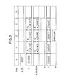
- the relationship between a numerical value P represented in two's complement (referred simply as "TC") and another value Q which emerges as a result of an overflow occurring when P exceeds the range of [-1, +1), is shown in Fig. 1. This relationship is obvious from the fact that, in TC representation, the addition of the least significant bit (LSB) to the maximum value on the positive side gives the maximum value on the negative side.
- LSB least significant bit
- P 2 is greater than 1 and including the sign bit is 01.001 in five-bit expression.
- P 2 herein is a positive value
- P 2 ' is negative.
- the result of the CA operation can be expected to return to a correct value in the dynamic range of -1, +1) even if it temporarily deviates therefrom.
- the result of the CA operation can be judged free from the overflows. If they are not equal, it can be judged that the overflow occurred in the direction where the counter number is greater.
- One embodiment of the invention illustrated in Fig. 2 includes an up-down counter 1, a zero detecting circuit 2, a sign bit detecting circuit 3, a single overflow detector 4, an adder 5 composed of full adders 51, 52, 53, and 54, an accumulator 7, addition-data input terminals 61, 62, 63 and 64 (the MSB of data is fed to the terminal 64), another addition-data input terminals 71, 72, 73, and 74 (the MSB of data is fed to the terminal 74), addition-result output terminals 81, 82, 83, and 84 (the MSB of data is supplied from the terminal 84), arithmetic-result output terminals 91, 92, 93, and 94, an overflow output terminal 9, an output terminal 10 for the circuit 3, a reset terminal 11 of the counter 1, and a reset terminal 75 of the accumulator 7.
- the up-down counter 1, the zero detecting circuit 2, the full adders 51-54, and the accumulator 7 may be composed of the types respectively described on pp.417-426, pp.202-208, pp.396-397, and pp.363-368 of "The TTL Data Book for Design Engineers", published in 1973 by Texas Instruments (Reference 6).
- terminals A, B, S, CI, and CO represent an input terminal for receiving an addition-data bit, an input terminal for receiving another addition-data bit, an output terminal for giving the result of addition, an input terminal for receiving a carry bit, and an output terminal for giving a carry bit, respectively.
- the up-down counter 1 is counted up in the positive direction when a signal "1" is fed to a terminal CONT and counted down in the negative direction when a signal "0" is fed to the terminal CONT.
- a terminal CLOCK is an input terminal for having the counter 1 count up or down by "1" in the direction set by the terminal CONT; terminals B1, B2, B3 and B4 are output terminals to supply the content of the counter (out of the data contained in the counter 1, the MSB is supplied from B1 and the LSB from B4); and a terminal RESET is a terminal to clear the content of the counter 1.
- the sign bit detecting circuit 3 is a circuit for outputing the MSB from the up-down counter 1 directly, and the single overflow detector 4 is an Exclusive OR (EOR) gate for detecting overflow data based on the technique described in Reference 5. Namely, this technique is used to detect an overflow when a carry input signal given to the terminal CI of the adder 54 and a carry output signal supplied from the terminal CO of the same adder are different from each other. With the present invention, a signal appearing at the terminal 10 shows the direction of the overflow. For instance, "0" appearing at the terminal 9 indicates the overflow in the positive direction and "1", one in the negative direction.
- EOR Exclusive OR
- the terminals 61, 62, 63, and 64 correspond to the outputs of the TEMP.REG.; the adder 5 corresponds to the ALU: the accumulator 7 to the ACCUMULATOR; and the terminals 91, 92, 93, and 94 and the path connected from the accumulator 7 to the adder 5 to the 8 BIT INTERNAL DATA BUS (the terminals 9 and 10 of the circuits 2 and 3 used in the present invention are led to the FLAG FLIP-FLOPS of Reference 3).
- zero is fed to the terminals 71-73, and to the terminals 61-64 are supplied data dependent on the input data.
- the output of the overflow detector 4 (consisting of an EOR gate), is "0" as shown in Fig. 3, thereby to stop the operation of the counter 1.
- the overflow detection is achieved by the present circuit in the following manner.
- the content "O" of the counter 1 is fed to the comparison terminal A of the zero detecting circuit 2 to be compared with the all "0" pattern fed to the comparison terminal B. Since the two input values given to the terminals A and B are identical with each other, "0" appears at the terminal 9 to indicate the occurrence of no overflow.
- the overflow detector 4 gives the Exclusive OR of the carry input signal "1" and the carry output signal "0" of the full adder 54 and, as illustrated in Fig. 3, supplies "1” as its output, thereby to indicate the occurrence of the overflow.
- "1" (indicative of a negative sign) is given from the sign bit output terminal 84 of the terminals 81-84 for supplying the result of addition, this value which has resulted from the overflow, indicates that the overflow has occurred in the positive direction.
- the counter since "1" is fed to both the terminals CLOCK and CONT of the counter 1, the counter is counted up by "1" to make its content "1" as shown in Fig. 3.
- the output of said detecting circuit 3 can judge whether the overflow is in the positive or the negative direction. Given an N-bit u-down counter, if overflowing in each direction occurs less than 2 N-1 - 1 times, the output of the circuit 3 can properly function.
- the present circuit for the CA operation does not detect any overflow if the final result of the CA operation is free from the overflow, which occurred during the CA operation, because the correct answer is obtained in the accumulator 7.
- the finally detected overflow is indicated whether it is in the positive or the negative direction.
- a processor to achieve the above-described digital signal processing for instance, such a processor as the one illustrated in Fig. 2-1 of Reference 3
- a stable second-order recursive digital filter can be achieved by merely adding a simple circuit without decreasing the data length for the arithmetic unit.
- the application of the present invention to a non-recursive digital filter or a correlator using this digital filter also enables the reduction of errors in the operation of the filter and correlator.
- the second embodiment comprises a single overflow detector 4, an adder 5 composed of full adders 51, 52, 53, and 5 1 1 , an accumulator 7, addition-data input terminals 61,62,63, and 6 1 1 , another addition-data input terminals 71,72,73, and 74, addition output terminals 81,82,83, and 84, arithmetic result output terminals 91,92,93, and 94, an auxiliary memory 20 for the overflow detection, a sign bit memory 21, an overflow occurrence memory 23, an Exclusive OR gate 22, AND gates 25 and 26, an OR gate 2 1 1 , output terminals 30 and 31, and reset terminals 32, 33, 34 and 75. It is to be noted that each circle attached to the gates 25 and 22 means the inversion of a signal given thereto.
- the memory 23 is an R-S flip-flop and the memory 21 is a D-type flip-flop.
- Said R-S flip-flop and D-type flip-flop may be composed of the ones described, respectively, on pages 128 and 129 of Reference 6.
- the memory 20 is a one-bit counting circuit, which is composed of the one described on pages 224-229 of Reference 6.
- reset signals are fed to the terminals 75, 32, 33, and 34 at time 0 to clear the accumulator 7, the overflow occurrence memory 23, the auxiliary memory 20 and the sign bit memory 21 (see Fig. 5).
- the first addition takes place at time 1 between zero of the accumulator 7 and a value P 1 (0.110) supplied to the terminals 61-64 with the result that no single overflow is caused.
- P 1 0.110 supplied to the terminals 61-64 with the result that no single overflow is caused.
- the outputs of the detector 4 and said memory 20 remain in "0".
- the gate 25 is closed, because the memory 20 remains in “O”, and the memory 23 also remains in "0". Consequently, the gate 24 gives a zero output, thereby to indicate the absence of overflow even in the CA operation.
- the value corresponding to P 1 in Fig. 1 which has been fed to the terminals 61-64, is stored in the accumulator 7.
- the contents of the memories 20, 23, and 21 are consequently changed as follows.
- the gates 25 and 26 assume the following states before each memory is subjected to such change. Namely, the gate 25 is opened in response to the output "1" from the detector 4 and the outputs "0" from the memories 20 and 23. The gate 26 is closed because of the output "0" from the memory 20. Accordingly, the contents of said memories are changed in the following manners. The content of the memory 20 is reversed to "1" by the output "1" given from the detector 4. Also, the content of the memory 23 remains in zero in response to the closed state of the gate 26.
- the content of the memory 21 becomes "1", which is the content of the sign bit given from the terminal 84, since the gate 25 is open.
- the output of the gate 24 is turned to "1" in response to the output "1" given from the memory 20, so that the occurrence of overflow may be indicated.
- the output of said memory 21 appears at the terminal 31 to indicate that the overflow is in the positive direction.
- the accumulator 7 is stored the value of P 2 ' shown in Fig. 1.
- the consecutive addition will be carried out at time 3, when a value a is added to P 2 ' of the accumulator 7 as referred to in Fig. 1.
- the adder 5 is in a state of overflow in the negative direction, causing the detector 4 to indicate "1" and the terminal 84 to give an output "0".
- the state of the memories 20, 23 and 21 are consequently changed as follows.
- the gates 22, 25 and 26 assume the following statesbefore each memory is subjected to such change. More definitely, the gate 25 is closed in response to the outputs "O" from the memory 23 and the outputs "1" from the detector 4 and the memory 20.
- the gate 22 is closed in response to the output "1" from the memory 21 and the output "0" from the terminal 84,.so that the gate 26 is closed. Accordingly, each of the memories is changed in the following manner.
- the content of the memory 20 is reversed to "0" in response to the output "1" of said detector.
- the memory 21 remains in “1” in response to the closed state of the gate 25, and the memory 23 remains in zero by the closed gate 26. Consequently, the output of the gate 24, is zero to indicate the absence of overflow and give the correct addition result, since the outputs of the memories 20 and 23 are zero.
- the single overflow detector 4 gives an output "1".
- the gate 22 is opened by the output "1" of the memory 21 supplied with “1" from the terminal 84 in response to said another overflow in the positive direction.
- the gate 26, consequently, becomes opened in response to the outputs "1" from the memory 20, the detector 4, and the gate 22.
- each content of the memories is changed as follows.
- the memory 20 remains in “0", because the detector 4 produced “I”.
- the memory 21 also remains in "1", because the gate 25 is closed.
- the memory 23 becomes "1" by the opened gate 26. Therefore, the gate 24 becomes opened to indicate the occurrence of overflow at the terminal 30 in response to the output "1" from the memory 23. This also reveals that the overflow occurred in the positive direction by "1" appearing at the terminal 34.
- the gate 25 always remains closed and the memory 23 never turns to zero unless a signal is fed to the terminal 32.
- "1" is continuously given by the detector in the subsequent consecutive additions, in whatever manner overflowing may occur so as to indicate the occurrence of overflow.
- the terminal 31 gives "1" to indicate that the overflow occurred in the positive direction, because the sign bit memory 21 is not rewritten by the closed gate 25.
- the present invention gives the final result of the CA operation free from overflow if any overflow that may occur in one direction in the course of the CA operation, is followed by another in the opposite direction and theoretically permits unlimited consecutive additions. Therefore, if this invention is applied to an arithmetic unit to achieve said digital signal processing, a stable second-order recursive digital filter can be achieved by merely adding a simple circuit without decreasing the data length of the arithmetic unit. Furthermore, since it theoretically permits unlimited consecutive additions, the invention also is applicable to the operation of a non-recursive digital filter having many taps and can thereby serve to reduce errors attributable to overflowing. The invention can be also applied to solve any overflow problem in the CA operation by the use of a subtractor.
Landscapes
- Physics & Mathematics (AREA)
- General Physics & Mathematics (AREA)
- Engineering & Computer Science (AREA)
- Computational Mathematics (AREA)
- Mathematical Analysis (AREA)
- Pure & Applied Mathematics (AREA)
- Theoretical Computer Science (AREA)
- Computing Systems (AREA)
- Mathematical Optimization (AREA)
- General Engineering & Computer Science (AREA)
- Complex Calculations (AREA)
Applications Claiming Priority (2)
| Application Number | Priority Date | Filing Date | Title |
|---|---|---|---|
| JP151534/79 | 1979-11-22 | ||
| JP15153479A JPS5674774A (en) | 1979-11-22 | 1979-11-22 | Arithmetic circuit with overflow detector |
Publications (2)
| Publication Number | Publication Date |
|---|---|
| EP0029706A1 true EP0029706A1 (fr) | 1981-06-03 |
| EP0029706B1 EP0029706B1 (fr) | 1986-02-05 |
Family
ID=15520609
Family Applications (1)
| Application Number | Title | Priority Date | Filing Date |
|---|---|---|---|
| EP80304145A Expired EP0029706B1 (fr) | 1979-11-22 | 1980-11-19 | Circuit arithmétique capable de détecter un débordement |
Country Status (5)
| Country | Link |
|---|---|
| US (1) | US4379338A (fr) |
| EP (1) | EP0029706B1 (fr) |
| JP (1) | JPS5674774A (fr) |
| CA (1) | CA1165891A (fr) |
| DE (1) | DE3071416D1 (fr) |
Cited By (4)
| Publication number | Priority date | Publication date | Assignee | Title |
|---|---|---|---|---|
| EP0136834A3 (en) * | 1983-09-02 | 1986-07-09 | Nec Corporation | A digital circuit performing an arithmetic operation with an overflow |
| EP0209014A3 (en) * | 1985-07-12 | 1990-05-09 | Siemens Aktiengesellschaft | Arrangement having a saturable carry-save adder |
| EP0281094A3 (en) * | 1987-03-04 | 1990-05-09 | Nippon Telegraph And Telephone Corporation | Counter |
| GB2236203A (en) * | 1989-08-30 | 1991-03-27 | Toshiba Kk | Data storage responsive to overflow detection |
Families Citing this family (36)
| Publication number | Priority date | Publication date | Assignee | Title |
|---|---|---|---|---|
| US4507725A (en) * | 1982-07-01 | 1985-03-26 | Rca Corporation | Digital filter overflow sensor |
| JPS6227864A (ja) * | 1985-07-29 | 1987-02-05 | Pioneer Electronic Corp | 累算回路 |
| JPS63228498A (ja) * | 1987-03-18 | 1988-09-22 | Fujitsu Ltd | 半導体記憶装置 |
| US5341482A (en) * | 1987-03-20 | 1994-08-23 | Digital Equipment Corporation | Method for synchronization of arithmetic exceptions in central processing units having pipelined execution units simultaneously executing instructions |
| JPS6491228A (en) * | 1987-09-30 | 1989-04-10 | Takeshi Sakamura | Data processor |
| US5038314A (en) * | 1989-11-17 | 1991-08-06 | Digital Equipment Corporation | Method and apparatus for correction of underflow and overflow |
| US5231600A (en) * | 1990-04-19 | 1993-07-27 | Bull Hn Information Systems Inc. | Overflow detector for anticipating producing invalid operands resulting from performing shift operations on such operands |
| US5272659A (en) * | 1990-06-26 | 1993-12-21 | Allied-Signal Inc. | Engine control with fixed point digital overflow prevention |
| JP2894015B2 (ja) * | 1991-06-28 | 1999-05-24 | 日本電気株式会社 | 桁あふれ検出方法および回路 |
| KR19980014906A (ko) * | 1996-08-17 | 1998-05-25 | 구자홍 | 누산기 |
| JP2002063151A (ja) * | 2000-08-22 | 2002-02-28 | Mitsubishi Electric Corp | マイクロコンピュータ |
| JP3833884B2 (ja) * | 2000-09-27 | 2006-10-18 | 株式会社東芝 | ディジタルフィルタ |
| US20030023836A1 (en) * | 2001-06-01 | 2003-01-30 | Michael Catherwood | Shadow register array control instructions |
| US7003543B2 (en) * | 2001-06-01 | 2006-02-21 | Microchip Technology Incorporated | Sticky z bit |
| US6985986B2 (en) * | 2001-06-01 | 2006-01-10 | Microchip Technology Incorporated | Variable cycle interrupt disabling |
| US6934728B2 (en) * | 2001-06-01 | 2005-08-23 | Microchip Technology Incorporated | Euclidean distance instructions |
| US7467178B2 (en) * | 2001-06-01 | 2008-12-16 | Microchip Technology Incorporated | Dual mode arithmetic saturation processing |
| US20030005269A1 (en) * | 2001-06-01 | 2003-01-02 | Conner Joshua M. | Multi-precision barrel shifting |
| US20020184566A1 (en) * | 2001-06-01 | 2002-12-05 | Michael Catherwood | Register pointer trap |
| US6952711B2 (en) * | 2001-06-01 | 2005-10-04 | Microchip Technology Incorporated | Maximally negative signed fractional number multiplication |
| US20030028696A1 (en) * | 2001-06-01 | 2003-02-06 | Michael Catherwood | Low overhead interrupt |
| US7007172B2 (en) * | 2001-06-01 | 2006-02-28 | Microchip Technology Incorporated | Modified Harvard architecture processor having data memory space mapped to program memory space with erroneous execution protection |
| US20030005268A1 (en) * | 2001-06-01 | 2003-01-02 | Catherwood Michael I. | Find first bit value instruction |
| US6975679B2 (en) * | 2001-06-01 | 2005-12-13 | Microchip Technology Incorporated | Configuration fuses for setting PWM options |
| US6937084B2 (en) * | 2001-06-01 | 2005-08-30 | Microchip Technology Incorporated | Processor with dual-deadtime pulse width modulation generator |
| US7020788B2 (en) * | 2001-06-01 | 2006-03-28 | Microchip Technology Incorporated | Reduced power option |
| US6976158B2 (en) * | 2001-06-01 | 2005-12-13 | Microchip Technology Incorporated | Repeat instruction with interrupt |
| JP3497852B1 (ja) * | 2002-06-06 | 2004-02-16 | 沖電気工業株式会社 | 演算方法および演算回路 |
| JP3813613B2 (ja) * | 2004-01-19 | 2006-08-23 | 日本テキサス・インスツルメンツ株式会社 | 加算回路 |
| US8495114B1 (en) | 2005-05-23 | 2013-07-23 | The Mathworks, Inc. | System and methods for determining attributes for arithmetic operations with fixed-point numbers |
| US7475295B2 (en) | 2005-10-28 | 2009-01-06 | International Business Machines Corporation | Intelligent watchdog circuit |
| US8484262B1 (en) | 2005-12-22 | 2013-07-09 | The Mathworks, Inc. | System and methods for determining attributes for arithmetic operations with fixed-point numbers |
| EP2579469B1 (fr) * | 2011-10-05 | 2014-08-13 | ST-Ericsson SA | Accumulation de valeurs de données |
| US10067744B2 (en) | 2016-12-08 | 2018-09-04 | International Business Machines Corporation | Overflow detection for sign-magnitude adders |
| DE112018005590T5 (de) | 2017-11-17 | 2020-10-15 | Semiconductor Energy Laboratory Co., Ltd. | Additionsverfahren, Halbleitervorrichtung und elektronisches Gerät |
| GB202214877D0 (en) * | 2022-10-10 | 2022-11-23 | Graphcore Ltd | Overflow event counter |
Citations (2)
| Publication number | Priority date | Publication date | Assignee | Title |
|---|---|---|---|---|
| FR1144749A (fr) * | 1955-01-24 | 1957-10-17 | Nat Res Dev | Machine à calculer électronique comportant des organes permettant d'éliminer les excès de longueur, d'effectuer certaines corrections et d'arrondir certains résultats |
| US3789206A (en) * | 1972-04-04 | 1974-01-29 | Bell Telephone Labor Inc | Threshold logic overflow detector for a three-input adder |
Family Cites Families (4)
| Publication number | Priority date | Publication date | Assignee | Title |
|---|---|---|---|---|
| US3700874A (en) * | 1971-03-04 | 1972-10-24 | Bell Telephone Labor Inc | Threshold logic overflow detector |
| US3970833A (en) * | 1975-06-18 | 1976-07-20 | The United States Of America As Represented By The Secretary Of The Navy | High-speed adder |
| JPS54554A (en) * | 1977-06-03 | 1979-01-05 | Hitachi Ltd | Digital filter |
| US4215415A (en) * | 1977-09-19 | 1980-07-29 | Nippon Electric Company, Ltd. | Recursive digital filter comprising a circuit responsive to first sum and feedback sign bits and second sum sign and integer bits for detecting overflow in the second sum |
-
1979
- 1979-11-22 JP JP15153479A patent/JPS5674774A/ja active Granted
-
1980
- 1980-11-19 EP EP80304145A patent/EP0029706B1/fr not_active Expired
- 1980-11-19 DE DE8080304145T patent/DE3071416D1/de not_active Expired
- 1980-11-21 US US06/209,250 patent/US4379338A/en not_active Expired - Lifetime
- 1980-11-21 CA CA000365230A patent/CA1165891A/fr not_active Expired
Patent Citations (2)
| Publication number | Priority date | Publication date | Assignee | Title |
|---|---|---|---|---|
| FR1144749A (fr) * | 1955-01-24 | 1957-10-17 | Nat Res Dev | Machine à calculer électronique comportant des organes permettant d'éliminer les excès de longueur, d'effectuer certaines corrections et d'arrondir certains résultats |
| US3789206A (en) * | 1972-04-04 | 1974-01-29 | Bell Telephone Labor Inc | Threshold logic overflow detector for a three-input adder |
Non-Patent Citations (1)
| Title |
|---|
| ELECTRONIC ENGINEERING, Vol. 49, No. 588, February 1977, page 18 London, G.B. K. WESTOWSKI: "Accumulating adder works with reversible counter" * Whole article * * |
Cited By (6)
| Publication number | Priority date | Publication date | Assignee | Title |
|---|---|---|---|---|
| EP0136834A3 (en) * | 1983-09-02 | 1986-07-09 | Nec Corporation | A digital circuit performing an arithmetic operation with an overflow |
| EP0209014A3 (en) * | 1985-07-12 | 1990-05-09 | Siemens Aktiengesellschaft | Arrangement having a saturable carry-save adder |
| EP0281094A3 (en) * | 1987-03-04 | 1990-05-09 | Nippon Telegraph And Telephone Corporation | Counter |
| GB2236203A (en) * | 1989-08-30 | 1991-03-27 | Toshiba Kk | Data storage responsive to overflow detection |
| US5197022A (en) * | 1989-08-30 | 1993-03-23 | Kabushiki Kaisha Toshiba | Overflow detection calculator and method of overflow determination |
| GB2236203B (en) * | 1989-08-30 | 1994-01-19 | Toshiba Kk | Calculation method and calculator using the same |
Also Published As
| Publication number | Publication date |
|---|---|
| DE3071416D1 (en) | 1986-03-20 |
| JPS5674774A (en) | 1981-06-20 |
| JPS6230467B2 (fr) | 1987-07-02 |
| EP0029706B1 (fr) | 1986-02-05 |
| US4379338A (en) | 1983-04-05 |
| CA1165891A (fr) | 1984-04-17 |
Similar Documents
| Publication | Publication Date | Title |
|---|---|---|
| EP0029706B1 (fr) | Circuit arithmétique capable de détecter un débordement | |
| US6874007B2 (en) | Apparatus and method for reducing precision of data | |
| US5936870A (en) | Arithmetic operating device for digital signal processing and method therefor | |
| EP0590597A2 (fr) | Appareil arithmétique | |
| US5508951A (en) | Arithmetic apparatus with overflow correction means | |
| JPS6211933A (ja) | 演算回路 | |
| US4561065A (en) | Arithmetic processing device using sampled input data and several previous output data | |
| US5111421A (en) | System for performing addition and subtraction of signed magnitude floating point binary numbers | |
| EP0693236B1 (fr) | Procede et structure de filtre fir numerique transpose destine a multiplier un signal d'entree binaire par des coefficents et procede de conception d'un filtre numerique transpose | |
| US5007009A (en) | Non-recovery parallel divider circuit | |
| US6947962B2 (en) | Overflow prediction algorithm and logic for high speed arithmetic units | |
| US5164914A (en) | Fast overflow and underflow limiting circuit for signed adder | |
| EP0238300B1 (fr) | Circuit de traitement de signaux numériques sériels | |
| EP0436905A2 (fr) | Additionneur à hautes performances utilisant la prédiction de retenues | |
| US5400271A (en) | Apparatus for and method of calculating sum of products | |
| US5331584A (en) | Discrete cosine transformation processor | |
| JPS6131488B2 (fr) | ||
| US4106100A (en) | Digital differential analyzer | |
| US5031137A (en) | Two input bit-serial multiplier | |
| Astola et al. | New digit-serial implementations of stack filters | |
| KR100309520B1 (ko) | 라운드오프기능을갖는승산방법및승산회로 | |
| RU2233024C2 (ru) | Способ и устройство для сжатия сигналов в формате с фиксированной запятой без введения смещения | |
| JPH09128213A (ja) | ブロックフローティング処理システムおよび方法 | |
| JPH07146777A (ja) | 演算装置 | |
| US12511103B2 (en) | Combinatorial logic circuits with feedback |
Legal Events
| Date | Code | Title | Description |
|---|---|---|---|
| PUAI | Public reference made under article 153(3) epc to a published international application that has entered the european phase |
Free format text: ORIGINAL CODE: 0009012 |
|
| AK | Designated contracting states |
Designated state(s): DE FR GB IT |
|
| 17P | Request for examination filed |
Effective date: 19810626 |
|
| RAP1 | Party data changed (applicant data changed or rights of an application transferred) |
Owner name: NEC CORPORATION |
|
| GRAA | (expected) grant |
Free format text: ORIGINAL CODE: 0009210 |
|
| AK | Designated contracting states |
Designated state(s): DE FR GB IT |
|
| REF | Corresponds to: |
Ref document number: 3071416 Country of ref document: DE Date of ref document: 19860320 |
|
| ET | Fr: translation filed | ||
| ITF | It: translation for a ep patent filed | ||
| PLBE | No opposition filed within time limit |
Free format text: ORIGINAL CODE: 0009261 |
|
| STAA | Information on the status of an ep patent application or granted ep patent |
Free format text: STATUS: NO OPPOSITION FILED WITHIN TIME LIMIT |
|
| 26N | No opposition filed | ||
| ITTA | It: last paid annual fee | ||
| PGFP | Annual fee paid to national office [announced via postgrant information from national office to epo] |
Ref country code: FR Payment date: 19991109 Year of fee payment: 20 |
|
| PGFP | Annual fee paid to national office [announced via postgrant information from national office to epo] |
Ref country code: GB Payment date: 19991117 Year of fee payment: 20 |
|
| PGFP | Annual fee paid to national office [announced via postgrant information from national office to epo] |
Ref country code: DE Payment date: 19991119 Year of fee payment: 20 |
|
| PG25 | Lapsed in a contracting state [announced via postgrant information from national office to epo] |
Ref country code: GB Free format text: LAPSE BECAUSE OF EXPIRATION OF PROTECTION Effective date: 20001118 |
|
| REG | Reference to a national code |
Ref country code: GB Ref legal event code: PE20 Effective date: 20001118 |