EP0030293A1 - Procédé et appareil pour obtention d'un rétrécissement uniforme d'un substrat laminé plan en céramique verte pendant le frittage - Google Patents
Procédé et appareil pour obtention d'un rétrécissement uniforme d'un substrat laminé plan en céramique verte pendant le frittage Download PDFInfo
- Publication number
- EP0030293A1 EP0030293A1 EP80107146A EP80107146A EP0030293A1 EP 0030293 A1 EP0030293 A1 EP 0030293A1 EP 80107146 A EP80107146 A EP 80107146A EP 80107146 A EP80107146 A EP 80107146A EP 0030293 A1 EP0030293 A1 EP 0030293A1
- Authority
- EP
- European Patent Office
- Prior art keywords
- substrate
- plate
- sintering
- ceramic
- coating layer
- Prior art date
- Legal status (The legal status is an assumption and is not a legal conclusion. Google has not performed a legal analysis and makes no representation as to the accuracy of the status listed.)
- Granted
Links
- 239000000758 substrate Substances 0.000 title claims abstract description 77
- 239000000919 ceramic Substances 0.000 title claims abstract description 38
- 238000005245 sintering Methods 0.000 title claims abstract description 37
- 238000000034 method Methods 0.000 title claims abstract description 11
- 229910052750 molybdenum Inorganic materials 0.000 claims abstract description 9
- 238000005524 ceramic coating Methods 0.000 claims abstract description 8
- 229910045601 alloy Inorganic materials 0.000 claims abstract description 7
- 239000000956 alloy Substances 0.000 claims abstract description 7
- 229910052715 tantalum Inorganic materials 0.000 claims abstract description 7
- 229910052721 tungsten Inorganic materials 0.000 claims abstract description 6
- 229910010293 ceramic material Inorganic materials 0.000 claims abstract description 5
- 239000002345 surface coating layer Substances 0.000 claims abstract description 4
- 238000010438 heat treatment Methods 0.000 claims abstract description 3
- 239000003870 refractory metal Substances 0.000 claims description 9
- 239000011247 coating layer Substances 0.000 claims 4
- 230000003746 surface roughness Effects 0.000 claims 2
- ZOKXTWBITQBERF-UHFFFAOYSA-N Molybdenum Chemical compound [Mo] ZOKXTWBITQBERF-UHFFFAOYSA-N 0.000 abstract description 8
- 239000011733 molybdenum Substances 0.000 abstract description 7
- GUVRBAGPIYLISA-UHFFFAOYSA-N tantalum atom Chemical compound [Ta] GUVRBAGPIYLISA-UHFFFAOYSA-N 0.000 abstract description 5
- WFKWXMTUELFFGS-UHFFFAOYSA-N tungsten Chemical compound [W] WFKWXMTUELFFGS-UHFFFAOYSA-N 0.000 abstract description 4
- 239000010937 tungsten Substances 0.000 abstract description 4
- 239000011819 refractory material Substances 0.000 abstract 2
- 238000005272 metallurgy Methods 0.000 description 10
- 239000004065 semiconductor Substances 0.000 description 7
- PNEYBMLMFCGWSK-UHFFFAOYSA-N aluminium oxide Inorganic materials [O-2].[O-2].[O-2].[Al+3].[Al+3] PNEYBMLMFCGWSK-UHFFFAOYSA-N 0.000 description 5
- 239000011248 coating agent Substances 0.000 description 4
- 238000000576 coating method Methods 0.000 description 4
- 238000012360 testing method Methods 0.000 description 4
- 229920005989 resin Polymers 0.000 description 3
- 239000011347 resin Substances 0.000 description 3
- 239000002002 slurry Substances 0.000 description 3
- 239000011230 binding agent Substances 0.000 description 2
- 238000001035 drying Methods 0.000 description 2
- 238000005304 joining Methods 0.000 description 2
- 239000000463 material Substances 0.000 description 2
- 239000000203 mixture Substances 0.000 description 2
- 239000002904 solvent Substances 0.000 description 2
- 125000006850 spacer group Chemical group 0.000 description 2
- 238000010345 tape casting Methods 0.000 description 2
- UFHFLCQGNIYNRP-UHFFFAOYSA-N Hydrogen Chemical compound [H][H] UFHFLCQGNIYNRP-UHFFFAOYSA-N 0.000 description 1
- 229910001182 Mo alloy Inorganic materials 0.000 description 1
- QCWXUUIWCKQGHC-UHFFFAOYSA-N Zirconium Chemical compound [Zr] QCWXUUIWCKQGHC-UHFFFAOYSA-N 0.000 description 1
- 239000000969 carrier Substances 0.000 description 1
- 229910052593 corundum Inorganic materials 0.000 description 1
- 238000005516 engineering process Methods 0.000 description 1
- 238000009472 formulation Methods 0.000 description 1
- 239000011521 glass Substances 0.000 description 1
- 229910052739 hydrogen Inorganic materials 0.000 description 1
- 239000001257 hydrogen Substances 0.000 description 1
- 238000010030 laminating Methods 0.000 description 1
- 239000010410 layer Substances 0.000 description 1
- 229910052751 metal Inorganic materials 0.000 description 1
- 239000002184 metal Substances 0.000 description 1
- 239000011236 particulate material Substances 0.000 description 1
- 239000004014 plasticizer Substances 0.000 description 1
- 229920002037 poly(vinyl butyral) polymer Polymers 0.000 description 1
- 238000002360 preparation method Methods 0.000 description 1
- 238000004080 punching Methods 0.000 description 1
- 238000012216 screening Methods 0.000 description 1
- 229910001845 yogo sapphire Inorganic materials 0.000 description 1
- 229910052726 zirconium Inorganic materials 0.000 description 1
Images

Classifications
-
- C—CHEMISTRY; METALLURGY
- C04—CEMENTS; CONCRETE; ARTIFICIAL STONE; CERAMICS; REFRACTORIES
- C04B—LIME, MAGNESIA; SLAG; CEMENTS; COMPOSITIONS THEREOF, e.g. MORTARS, CONCRETE OR LIKE BUILDING MATERIALS; ARTIFICIAL STONE; CERAMICS; REFRACTORIES; TREATMENT OF NATURAL STONE
- C04B35/00—Shaped ceramic products characterised by their composition; Ceramics compositions; Processing powders of inorganic compounds preparatory to the manufacturing of ceramic products
- C04B35/622—Forming processes; Processing powders of inorganic compounds preparatory to the manufacturing of ceramic products
- C04B35/64—Burning or sintering processes
-
- H—ELECTRICITY
- H05—ELECTRIC TECHNIQUES NOT OTHERWISE PROVIDED FOR
- H05K—PRINTED CIRCUITS; CASINGS OR CONSTRUCTIONAL DETAILS OF ELECTRIC APPARATUS; MANUFACTURE OF ASSEMBLAGES OF ELECTRICAL COMPONENTS
- H05K1/00—Printed circuits
- H05K1/02—Details
- H05K1/03—Use of materials for the substrate
- H05K1/0306—Inorganic insulating substrates, e.g. ceramic, glass
-
- H—ELECTRICITY
- H05—ELECTRIC TECHNIQUES NOT OTHERWISE PROVIDED FOR
- H05K—PRINTED CIRCUITS; CASINGS OR CONSTRUCTIONAL DETAILS OF ELECTRIC APPARATUS; MANUFACTURE OF ASSEMBLAGES OF ELECTRICAL COMPONENTS
- H05K3/00—Apparatus or processes for manufacturing printed circuits
- H05K3/46—Manufacturing multilayer circuits
- H05K3/4611—Manufacturing multilayer circuits by laminating two or more circuit boards
-
- H—ELECTRICITY
- H05—ELECTRIC TECHNIQUES NOT OTHERWISE PROVIDED FOR
- H05K—PRINTED CIRCUITS; CASINGS OR CONSTRUCTIONAL DETAILS OF ELECTRIC APPARATUS; MANUFACTURE OF ASSEMBLAGES OF ELECTRICAL COMPONENTS
- H05K3/00—Apparatus or processes for manufacturing printed circuits
- H05K3/46—Manufacturing multilayer circuits
- H05K3/4611—Manufacturing multilayer circuits by laminating two or more circuit boards
- H05K3/4626—Manufacturing multilayer circuits by laminating two or more circuit boards characterised by the insulating layers or materials
- H05K3/4629—Manufacturing multilayer circuits by laminating two or more circuit boards characterised by the insulating layers or materials laminating inorganic sheets comprising printed circuits, e.g. green ceramic sheets
Definitions
- This invention relates to a method of achieving uniform shrinkage in a laminated planar green ceramic substrate during sintering and apparatus therefor.
- a uniform shrinkage rate over the entire area of the substrate is very important to thereby minimize distortion of the surface patterns and metallurgy.
- the green ceramic substrate will shrink anywhere from 15% to 20%. This shrinkage must be uniform in a substrate for a device package containing very small metallurgy patterns that must match up with testing apparatus and ultimately the semiconductor devices to be mounted thereon.
- Future semiconductor packages will be required to mount many highly integrated semiconductor devices, each with hundreds of circuits, on a single substrate, and interconnect these devices into an operative system. This will require that the area of the package be significantly increased, as compared to single device packages now in common usage, the wiring density increased, and that many closely spaced bonding terminals for connections to the semiconductor devices be provided.
- a structure that can potentially meet future high density package requirements is the multilayer ceramic substrate. In this substrate the metallurgy is buried within the substrate, making possible very complex and intricate wiring. This technology is well known and described in U.S. Patents 3,540,894, 3,726,002, 3,770,529, 3,838,204, 3,852,877, 3,899,554, 4,109,377, and others.
- the basic process consists of forming a ceramic slurry of a particulate ceramic material, a resin binder, and a solvent for the binder, doctor blading the slurry and drying to produce ceramic green sheets, punching holes in and screening conductive lines on the green sheets, laminating the sheets, and sintering.
- the substrate will shrink approximately 17% depending upon the materials, the sintering conditions, etc. This decrease in size can be accommodated by starting with a geometry that is larger than the final desired size by the amount of shrinkage.
- any variation of the shrinkage in the substrate presents serious problems in testing and in ultimately joining the devices to the substrate. If the shrinkage varies in different areas of the substrate,.the substrate is frequently useless because of the resultant distortion.
- Substrates are conventionally supported on a cured ceramic plate, typically A1 2 0 3 plate during the sintering operation. This sintering procedure has not been satisfactory for achieving uniform shrinkage in all areas of the substrate during sintering.
- the object of this invention is to provide a new method for minimizing sintering shrinkage distortion of a planar laminated multilayer ceramic substrate by minimizing thermal gradients in the planar ceramic substrate during sintering, and preventing bonding of a planar ceramic substrate to its support during a sintering operation.
- Another object of this invention is to provide a new setter plate for supporting a laminated multilayer ceramic substrate during the sintering operation that minimizes shrinkage distortion by minimizing thermal gradients within the ceramic substrate being sintered and preventing bonding of the ceramic substrate being sintered to the plate.
- the object is achieved in accordance with the method of the invention by placing the substrate on a flat, relatively thick plate of refractory metal selected from the group consisting of molybdenum, tungsten, tantalum and alloys thereof, said plate provided with a thin surface coating layer of a ceramic material, and subsequently heating the substrate to a sintering temperature and maintaining the temperature for a time sufficient to sinter the substrate.
- a flat, relatively thick plate of refractory metal selected from the group consisting of molybdenum, tungsten, tantalum and alloys thereof
- a setter plate which comprises a flat plate of a refractory metal selected from the group consisting of molybdenum, tantalum and tungsten, and high temperature alloys which include major proportions of the refractory metals, and a thin ceramic coating on at least the top surface of the 'flat plate.
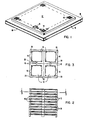
- a setter plate 10 of the invention on which is supported a multilayer ceramic substrate 12.
- the substrate 12 is initially formed of a plurality of green ceramic sheets, each with via holes in a unique metallurgy pattern.
- the sheets are assembled to provide complex internal metallurgy circuits that interconnect devices which are subsequently joined to the device terminal pads.
- substrate 12 has a complex top surface metallurgy configuration which includes clusters of device terminal pads 14, which can be surrounded with one or more rows of engineering change pads 16.
- the completed sintered substrate will ordinarily be tested after sintering to check the integrity of the internal circuitry, have integrated circuit semiconductor devices joined to the terminal pads, and subsequently have engineering change wires bonded selectively to the engineering change pads.
- the testing, device joining and engineering change wire bonding will ordinarily be accomplished with highly automated apparatus. It is of utmost importance that all of the pads in the surface metallurgy configuration be located in relatively predictable locations. This requires that the shrinkage of the substrate 12 be uniform during the sintering operation, where the average shrinkage rate can vary from 17 to 20%.
- the setter plate 10 of the invention is formed of a refractory metal such as molybdenum, tantalum, or tungsten, or alloys which include major proportions of refractory metals.
- TZM molybdenum alloy with a composition of 99.42% molybdenum, 0.5% tantalum, and 0.08% zirconium.
- Plate 10 can be of any suitable thickness necessary to support the substrate being sintered in the high temperature environment of a sintering furnace. In general the ratio of the length or width to the thickness is in the range of 40 to 1..
- Setter plate 10 has a thin ceramic coating 18 on at least the top surface. The coating can be provided on the bottom surface and edges as well, if desired. Coating 18 prevents bonding of the ceramic substrate being sintered to the plate, and also resists wear.
- a preferred coating material is A1 2 0 3 which is plasma sprayed to a thickness in the range of 0.05 mm to 0.25 mm, more preferably in the range of 0.08 mm to 0.125 mm.
- the surface finish of the ceramic coating 18 is in the range of 3 to 6 micro meters, more preferably from 3 to 5 micro meters.
- the multilayer ceramic substrate 12 rests on setter plate 10, free of restraint.
- the substrate shrinks from 15 to 20% and must be free to shift on its support to accommodate this shrinkage.
- the surface finish of the coating 18 is very important in that it must be sufficiently rough to prevent the substrate from sticking to the plate, and also be sufficiently smooth to allow limited movement of portions of the substrate. Any restraint of the substrate will result in distortion of the final ceramic substrate, which is unacceptable.
- Another requirement is that the substrate temperature be maintained as uniform as possible.
- the thermal conductivity of the refractory setter tile of the invention is from 5 to 20 times that of the conventional A1 2 0 3 in the temperature range of 1250°C to 1650°C, the critical range in which the substrate densifies.
- the setter tile of the invention thus maintains a uniform substrate temperature.
- Flatness is also a rigorous requirement for sintering multilayer ceramic substrates. Because the substrate usually conforms to the surface on which it is sintered, it is necessary that the supporting plate remain flat and rigid at temperatures of 1550°C to 1650°C which is a common sintering temperature range.
- Molybdenum and the other mentioned refractory metals meets this requirement using thicknesses from 2 to 3 times less than those of tiles of ceramic formulations. This results in increased throughput, since more of the kiln area can be used for product and less for carriers.
- Figs. 2 and 3 of the drawings there is illustrated a typical arrangement of setter tiles, substrates, and spacer blocks for sintering.
- Tiles 10 are . supported on A1 2 0 3 spacer blocks 20 which are arranged in tiers.
- a multilayer ceramic substrate 12 rests free of restraint on each tile 10.
- Fig. 3 illustrates the placement of the spacer blocks and substrates 12 relative to'tiles 10. The arrangement illustrated is a typical one and obviously other satisfactory arrangements of the tiles and blocks can be made.
- the substrates were prepared by doctor blading and drying a ceramic slurry containing particulate material of 89% Al 2 O 3 , 11% glass frit, a polyvinylbutyral resin, a solvent for the resin, and a plasticizer.
- a ceramic slurry containing particulate material of 89% Al 2 O 3 , 11% glass frit, a polyvinylbutyral resin, a solvent for the resin, and a plasticizer.
- Each substrate was formed of 28 green ceramic sheets with an overall thickness of 5.6 mm.. The thickness of a single sheet was 0.2 mm.
- the inner ceramic sheets were blank, i.e., no vias or printed lines.
- the outer sheets contained metal filled vias and pads suitable for making connections to semiconductor devices and engineering change pads on the top surface, and I/O pins on the bottom surface.
- the multilayer ceramic substrates each measured 109 mm by 109 mm.
- the top surface metallurgy included 100 fiducial marks arranged in a rectangular grid.
- the setter tiles were formed of molybdenum with a thickness of 6.35 mm.
- the tiles measured 140 mm x 140 mm.
- the surfaces of the tiles were ground flat (25 pm TIR), and coated with 125 ⁇ m thick layer of plasma flame-sprayed alumina with a surface finish of 5 ⁇ m CLA.
- the remaining 20 multilayer ceramic substrates were placed on ground alumina setter tiles which were also arranged in stacks as shown in Figs. 2 and 3.
- the alumina setter tiles were of the same dimensions as the tiles of the invention except that the thickness was greater which is necessitated by the decrease strength during the sintering operation.
- the substrates supported on the respective setter tiles were introduced into a sintering furnace and exposed to a sintering cycle when the temperature was increased for 15 hours until it reached a temperature of 1560° C, and held at the temperature for 3 hours.
- the furnace was allowed to cool down to about 100°C over a period of 16 hours.
- hydrogen was introduced and maintained in the furnace.
- the location of each fidicial mark was carefully measured and a distortion map made for each substrate from the resultant data.
- the distortion map consisted of a first grid of dotted lines resulting from calculating the theoretical location of each of the fidicial marks and drawing X and Y lines through the points.
- FIG. 4 which depicts a distortion map of a ceramic substrate supported on an A1 2 0 3 tile shows significantly more distortion than a substrate supported on the setter tile of the invention as depicted in Fig. 5. This clearly illustrates the superior operating characteristics of the setter tile of the invention in reducing distortion during the sintering operation.
- the reduction in distortion when using the tile of the invention is believed to result from improved thermal conductivity of the molybdenum metal, and also the surface interface with the tile produced by the plasma flame-sprayed alumina.
Landscapes
- Chemical & Material Sciences (AREA)
- Engineering & Computer Science (AREA)
- Manufacturing & Machinery (AREA)
- Ceramic Engineering (AREA)
- Inorganic Chemistry (AREA)
- Materials Engineering (AREA)
- Structural Engineering (AREA)
- Organic Chemistry (AREA)
- Production Of Multi-Layered Print Wiring Board (AREA)
- Furnace Charging Or Discharging (AREA)
- Producing Shaped Articles From Materials (AREA)
Applications Claiming Priority (2)
| Application Number | Priority Date | Filing Date | Title |
|---|---|---|---|
| US06/101,305 US4259061A (en) | 1979-12-07 | 1979-12-07 | Method of achieving uniform sintering shrinkage in a laminated planar green ceramic substrate and apparatus therefor |
| US101305 | 1979-12-07 |
Publications (2)
| Publication Number | Publication Date |
|---|---|
| EP0030293A1 true EP0030293A1 (fr) | 1981-06-17 |
| EP0030293B1 EP0030293B1 (fr) | 1984-02-01 |
Family
ID=22283945
Family Applications (1)
| Application Number | Title | Priority Date | Filing Date |
|---|---|---|---|
| EP80107146A Expired EP0030293B1 (fr) | 1979-12-07 | 1980-11-18 | Procédé et appareil pour obtention d'un rétrécissement uniforme d'un substrat laminé plan en céramique verte pendant le frittage |
Country Status (5)
| Country | Link |
|---|---|
| US (1) | US4259061A (fr) |
| EP (1) | EP0030293B1 (fr) |
| JP (1) | JPS5684374A (fr) |
| CA (1) | CA1129268A (fr) |
| DE (1) | DE3066432D1 (fr) |
Cited By (5)
| Publication number | Priority date | Publication date | Assignee | Title |
|---|---|---|---|---|
| FR2549944A1 (fr) * | 1983-07-27 | 1985-02-01 | Norton Co | Plaque en materiau refractaire pour fours de cuisson d'articles ceramiques |
| EP0236006A3 (en) * | 1986-02-20 | 1989-07-26 | Ishizuka Garasu Kabushiki Kaisha | Sheet for use in firing base plates |
| WO1991019149A1 (fr) * | 1990-06-01 | 1991-12-12 | Groom Bryan Ltd | Appareil de support pour un article |
| EP1041864A3 (fr) * | 1999-04-02 | 2000-12-20 | Gisulfo Baccini | Plaque pour base de support flexible pour circuits electroniques |
| CN109500544A (zh) * | 2018-10-16 | 2019-03-22 | 福建夜光达科技股份有限公司 | 一种微结构模具的薄厚间隔叠片式制作方法 |
Families Citing this family (43)
| Publication number | Priority date | Publication date | Assignee | Title |
|---|---|---|---|---|
| JPS5746662A (en) * | 1980-09-04 | 1982-03-17 | Toshiba Corp | Semiconductor rectifier |
| US4536153A (en) * | 1983-02-23 | 1985-08-20 | Anthony Frank H | Refractory shelf for home hobbyist kiln and method of making kiln |
| US4545761A (en) * | 1984-12-10 | 1985-10-08 | At&T Technologies, Inc. | Method and apparatus for securing articles in place on a substrate |
| US5130067A (en) * | 1986-05-02 | 1992-07-14 | International Business Machines Corporation | Method and means for co-sintering ceramic/metal mlc substrates |
| JPS6345304U (fr) * | 1986-09-12 | 1988-03-26 | ||
| JPH01102134U (fr) * | 1987-12-28 | 1989-07-10 | ||
| US4931331A (en) * | 1988-04-05 | 1990-06-05 | Owens Charles R | Laminated tile product, method for producing the same and method for installing the same |
| WO1991010630A1 (fr) * | 1990-01-18 | 1991-07-25 | E.I. Du Pont De Nemours And Company | Procede de reduction du retrecissement lors de la cuisson de corps en ceramique brute |
| JPH0647499B2 (ja) * | 1990-03-28 | 1994-06-22 | 日本碍子株式会社 | セラミックス製品の焼成方法 |
| GB9010833D0 (en) * | 1990-05-15 | 1990-07-04 | Electrotech Research Limited | Workpiece support |
| US5254191A (en) * | 1990-10-04 | 1993-10-19 | E. I. Du Pont De Nemours And Company | Method for reducing shrinkage during firing of ceramic bodies |
| EP0484130B1 (fr) * | 1990-10-30 | 1995-12-27 | Kabushiki Kaisha Toshiba | Grille pour traitement thermique à température haute |
| US5603875A (en) * | 1993-06-11 | 1997-02-18 | Aerospace Coating Systems, Inc. | Method for producing ceramic-based components |
| US5336453B1 (en) * | 1993-06-11 | 1996-07-23 | Connecticut Innovations Inc | Method for producing ceramic-based electronic components |
| US5388345A (en) * | 1993-11-04 | 1995-02-14 | Corning Incorporated | Dielectric drying of metal structures |
| US5406058A (en) * | 1993-11-30 | 1995-04-11 | Corning Incorporated | Apparatus for drying ceramic structures using dielectric energy |
| US5833452A (en) * | 1994-12-15 | 1998-11-10 | M-C Power Corporation | Coated metal sintering carriers for fuel cell electrodes |
| US5755570A (en) * | 1995-05-26 | 1998-05-26 | International Business Machines Corporation | Apparatus for in situ environment sensitive sealing and/or product controlling |
| US5628849A (en) * | 1995-05-26 | 1997-05-13 | International Business Machines Corporation | Method for in-situ environment sensitive sealing and/or product controlling |
| US5759669A (en) * | 1995-12-22 | 1998-06-02 | International Business Machines Corporation | Apparatus and method for screening green sheet with via hole using porous backing material |
| US5874162A (en) * | 1996-10-10 | 1999-02-23 | International Business Machines Corporation | Weighted sintering process and conformable load tile |
| JPH11222605A (ja) * | 1998-02-04 | 1999-08-17 | Mitsubishi Electric Corp | 摺動部品の製造方法およびその製造方法により製造された噴射弁の旋回流発生体 |
| JP4205902B2 (ja) * | 2001-09-20 | 2009-01-07 | イソライト工業株式会社 | セラミックセッター及びその製造方法 |
| US7332228B2 (en) * | 2003-02-25 | 2008-02-19 | A.L.M.T. Corporation | Coated refractory metal plate having oxide surface layer, and setter which uses the same and which is used in sintering |
| DE102004056879B4 (de) * | 2004-10-27 | 2008-12-04 | Curamik Electronics Gmbh | Verfahren zum Herstellen eines Metall-Keramik-Substrates |
| DE102006048465B4 (de) * | 2006-10-11 | 2009-11-26 | Kerafol Keramische Folien Gmbh | Verfahren zur Herbeiführung eines definierten Schrumpfungsverhaltens eines keramischen Grünfolienabschnittes und Verwendung eines flachen Körpers als Brennunterlage |
| US9205571B2 (en) * | 2012-04-18 | 2015-12-08 | Nitto Denko Corporation | Method and apparatus for sintering flat ceramics |
| US9206086B2 (en) * | 2012-04-18 | 2015-12-08 | Nitto Denko Corporation | Method and apparatus for sintering flat ceramics |
| US9362546B1 (en) | 2013-01-07 | 2016-06-07 | Quantumscape Corporation | Thin film lithium conducting powder material deposition from flux |
| US10403931B2 (en) | 2013-10-07 | 2019-09-03 | Quantumscape Corporation | Garnet materials for Li secondary batteries and methods of making and using garnet materials |
| WO2015088839A1 (fr) * | 2013-12-10 | 2015-06-18 | Saint-Gobain Ceramics & Plastics, Inc. | Article réfractaire |
| KR20240059640A (ko) | 2015-04-16 | 2024-05-07 | 퀀텀스케이프 배터리, 인코포레이티드 | 고체 전해질 제조를 위한 리튬 함유 가넷 세터 플레이트 |
| JP2018528916A (ja) | 2015-07-21 | 2018-10-04 | クアンタムスケイプ コーポレイション | グリーンガーネット薄膜を流延及び焼結するプロセス及び材料 |
| US9966630B2 (en) | 2016-01-27 | 2018-05-08 | Quantumscape Corporation | Annealed garnet electrolyte separators |
| US20170331092A1 (en) | 2016-05-13 | 2017-11-16 | Quantumscape Corporation | Solid electrolyte separator bonding agent |
| US11158880B2 (en) | 2016-08-05 | 2021-10-26 | Quantumscape Battery, Inc. | Translucent and transparent separators |
| US11916200B2 (en) | 2016-10-21 | 2024-02-27 | Quantumscape Battery, Inc. | Lithium-stuffed garnet electrolytes with a reduced surface defect density and methods of making and using the same |
| WO2018236394A1 (fr) | 2017-06-23 | 2018-12-27 | Quantumscape Corporation | Électrolytes de grenat remplis de lithium avec des inclusions de phase secondaire |
| US10347937B2 (en) | 2017-06-23 | 2019-07-09 | Quantumscape Corporation | Lithium-stuffed garnet electrolytes with secondary phase inclusions |
| WO2019090360A1 (fr) | 2017-11-06 | 2019-05-09 | Quantumscape Corporation | Films minces de grenat remplis de lithium et pastilles présentant une surface oxyfluorée et/ou fluorée et procédés de fabrication et d'utilisation des films minces et des pastilles |
| US12046712B2 (en) | 2018-06-06 | 2024-07-23 | Quantumscape Battery, Inc. | Solid-state battery |
| US12469876B2 (en) | 2020-01-15 | 2025-11-11 | Quantumscape Battery, Inc. | High green density ceramics for battery |
| CN112503948B (zh) * | 2020-10-28 | 2021-10-22 | 横店集团东磁股份有限公司 | 一种提高烧制铁氧制品的尺寸精度的承载装置及方法 |
Citations (4)
| Publication number | Priority date | Publication date | Assignee | Title |
|---|---|---|---|---|
| DE6601206U (de) * | Rosenthal Ag | Temperaturwechselbeständige Unterlage als Brennhilfsmittel | ||
| GB1219518A (en) * | 1967-12-30 | 1971-01-20 | Nukem Gmbh | Metal boats for use in sintering furnaces |
| DE2425526B2 (de) * | 1974-05-27 | 1977-06-23 | Reaktor-Brennelement Union Gmbh, 6450 Hanau | Transportschiffchen fuer hochtemperaturdurchlaufofen |
| US4057702A (en) * | 1973-10-31 | 1977-11-08 | Automatisme & Technique | Process and plant for the fritting of ceramic products |
Family Cites Families (3)
| Publication number | Priority date | Publication date | Assignee | Title |
|---|---|---|---|---|
| US3792139A (en) * | 1972-08-09 | 1974-02-12 | Us Army | Process for flattening alumina substrates |
| DE2315797C3 (de) * | 1973-03-29 | 1981-07-30 | Siemens AG, 1000 Berlin und 8000 München | Verfahren zur Herstellung von Keramiksubstraten für Dünnschichtschaltungen |
| GB1499662A (en) * | 1974-04-02 | 1978-02-01 | Acme Marls Ltd | Support assembly for supporting pottery articles |
-
1979
- 1979-12-07 US US06/101,305 patent/US4259061A/en not_active Expired - Lifetime
-
1980
- 1980-10-07 CA CA361,714A patent/CA1129268A/fr not_active Expired
- 1980-10-20 JP JP14583680A patent/JPS5684374A/ja active Granted
- 1980-11-18 EP EP80107146A patent/EP0030293B1/fr not_active Expired
- 1980-11-18 DE DE8080107146T patent/DE3066432D1/de not_active Expired
Patent Citations (4)
| Publication number | Priority date | Publication date | Assignee | Title |
|---|---|---|---|---|
| DE6601206U (de) * | Rosenthal Ag | Temperaturwechselbeständige Unterlage als Brennhilfsmittel | ||
| GB1219518A (en) * | 1967-12-30 | 1971-01-20 | Nukem Gmbh | Metal boats for use in sintering furnaces |
| US4057702A (en) * | 1973-10-31 | 1977-11-08 | Automatisme & Technique | Process and plant for the fritting of ceramic products |
| DE2425526B2 (de) * | 1974-05-27 | 1977-06-23 | Reaktor-Brennelement Union Gmbh, 6450 Hanau | Transportschiffchen fuer hochtemperaturdurchlaufofen |
Cited By (8)
| Publication number | Priority date | Publication date | Assignee | Title |
|---|---|---|---|---|
| FR2549944A1 (fr) * | 1983-07-27 | 1985-02-01 | Norton Co | Plaque en materiau refractaire pour fours de cuisson d'articles ceramiques |
| EP0236006A3 (en) * | 1986-02-20 | 1989-07-26 | Ishizuka Garasu Kabushiki Kaisha | Sheet for use in firing base plates |
| WO1991019149A1 (fr) * | 1990-06-01 | 1991-12-12 | Groom Bryan Ltd | Appareil de support pour un article |
| US5362231A (en) * | 1990-06-01 | 1994-11-08 | Bryan Groom | Article support apparatus |
| EP1041864A3 (fr) * | 1999-04-02 | 2000-12-20 | Gisulfo Baccini | Plaque pour base de support flexible pour circuits electroniques |
| US6409138B1 (en) | 1999-04-02 | 2002-06-25 | Gisulfo Baccini | Supporting plate for flexible base supports for electronic circuits |
| CN109500544A (zh) * | 2018-10-16 | 2019-03-22 | 福建夜光达科技股份有限公司 | 一种微结构模具的薄厚间隔叠片式制作方法 |
| CN109500544B (zh) * | 2018-10-16 | 2020-11-06 | 福建夜光达科技股份有限公司 | 一种微结构模具的薄厚间隔叠片式制作方法 |
Also Published As
| Publication number | Publication date |
|---|---|
| EP0030293B1 (fr) | 1984-02-01 |
| US4259061A (en) | 1981-03-31 |
| JPS5684374A (en) | 1981-07-09 |
| JPS6343914B2 (fr) | 1988-09-01 |
| DE3066432D1 (en) | 1984-03-08 |
| CA1129268A (fr) | 1982-08-10 |
Similar Documents
| Publication | Publication Date | Title |
|---|---|---|
| US4259061A (en) | Method of achieving uniform sintering shrinkage in a laminated planar green ceramic substrate and apparatus therefor | |
| EP0043029B1 (fr) | Substrat céramique multicouches obtenu par frittage et procédé pour sa fabrication | |
| US4521449A (en) | Process for forming a high density metallurgy system on a substrate and structure thereof | |
| EP0043955B1 (fr) | Procédé de formation d'une structure en verre-céramique | |
| US4753694A (en) | Process for forming multilayered ceramic substrate having solid metal conductors | |
| EP0163172B1 (fr) | Procédé de formation d'une structure de métallisation sur la surface d'un substrat céramique | |
| EP0144046B1 (fr) | Procédé pour la formation d'un dessin métallurgique à surface densifiée sur ou dans un substrat fritté diélectrique | |
| US4879156A (en) | Multilayered ceramic substrate having solid non-porous metal conductors | |
| IL95780A (en) | Three dimensional microcircuit structure and process for fabricating the same from ceramic tape | |
| US6020750A (en) | Wafer test and burn-in platform using ceramic tile supports | |
| KR101555405B1 (ko) | 세라믹 기판 및 그 제조방법 | |
| US5302219A (en) | Method for obtaining via patterns in ceramic sheets | |
| JPH08139230A (ja) | セラミック回路基板とその製造方法 | |
| US4336088A (en) | Method of fabricating an improved multi-layer ceramic substrate | |
| US4562513A (en) | Process for forming a high density metallurgy system on a substrate and structure thereof | |
| US5733640A (en) | Fired body for manufacturing a substrate | |
| JP2955442B2 (ja) | セラミックス回路基板の製造方法 | |
| EP0078370A1 (fr) | Méthode pour détecter les résidus de verre dans la fabrication de substrats en céramiques pour semi-conducteurs | |
| JP2727652B2 (ja) | 窒化アルミニウム基板の焼成方法 | |
| JPH06164143A (ja) | 多層ハイブリッド回路の製造方法 | |
| CN115745577B (zh) | 一种超薄低温烧结陶瓷基板的制备方法 | |
| JP2002124446A (ja) | 半導体製造・検査装置用セラミックヒータ | |
| JPH11233674A (ja) | セラミックス基板の製造方法 | |
| JPH0828579B2 (ja) | セラミツク多層基板の製造方法 | |
| Stahl | Boeblingen, West Germany |
Legal Events
| Date | Code | Title | Description |
|---|---|---|---|
| PUAI | Public reference made under article 153(3) epc to a published international application that has entered the european phase |
Free format text: ORIGINAL CODE: 0009012 |
|
| AK | Designated contracting states |
Kind code of ref document: A1 Designated state(s): DE FR GB IT Designated state(s): DE FR GB IT |
|
| 17P | Request for examination filed |
Effective date: 19810807 |
|
| ITF | It: translation for a ep patent filed | ||
| GRAA | (expected) grant |
Free format text: ORIGINAL CODE: 0009210 |
|
| AK | Designated contracting states |
Kind code of ref document: B1 Designated state(s): DE FR GB IT Designated state(s): DE FR GB IT |
|
| REF | Corresponds to: |
Ref document number: 3066432 Country of ref document: DE Date of ref document: 19840308 |
|
| ET | Fr: translation filed | ||
| PLBE | No opposition filed within time limit |
Free format text: ORIGINAL CODE: 0009261 |
|
| STAA | Information on the status of an ep patent application or granted ep patent |
Free format text: STATUS: NO OPPOSITION FILED WITHIN TIME LIMIT |
|
| 26N | No opposition filed | ||
| ITTA | It: last paid annual fee | ||
| PGFP | Annual fee paid to national office [announced via postgrant information from national office to epo] |
Ref country code: GB Payment date: 19941013 Year of fee payment: 15 |
|
| PGFP | Annual fee paid to national office [announced via postgrant information from national office to epo] |
Ref country code: FR Payment date: 19941103 Year of fee payment: 15 |
|
| PGFP | Annual fee paid to national office [announced via postgrant information from national office to epo] |
Ref country code: DE Payment date: 19941201 Year of fee payment: 15 |
|
| PG25 | Lapsed in a contracting state [announced via postgrant information from national office to epo] |
Ref country code: GB Effective date: 19951118 |
|
| GBPC | Gb: european patent ceased through non-payment of renewal fee |
Effective date: 19951118 |
|
| PG25 | Lapsed in a contracting state [announced via postgrant information from national office to epo] |
Ref country code: FR Effective date: 19960731 |
|
| PG25 | Lapsed in a contracting state [announced via postgrant information from national office to epo] |
Ref country code: DE Effective date: 19960801 |
|
| REG | Reference to a national code |
Ref country code: FR Ref legal event code: ST |