EP0030300A1 - Circuit pour un enregistreur de données magnétiques et procédé d'utilisation d'enregistreurs de données magnétiques - Google Patents
Circuit pour un enregistreur de données magnétiques et procédé d'utilisation d'enregistreurs de données magnétiques Download PDFInfo
- Publication number
- EP0030300A1 EP0030300A1 EP80107233A EP80107233A EP0030300A1 EP 0030300 A1 EP0030300 A1 EP 0030300A1 EP 80107233 A EP80107233 A EP 80107233A EP 80107233 A EP80107233 A EP 80107233A EP 0030300 A1 EP0030300 A1 EP 0030300A1
- Authority
- EP
- European Patent Office
- Prior art keywords
- signal
- circuit
- transducer
- data
- data signal
- Prior art date
- Legal status (The legal status is an assumption and is not a legal conclusion. Google has not performed a legal analysis and makes no representation as to the accuracy of the status listed.)
- Granted
Links
- 238000000034 method Methods 0.000 title claims description 20
- 230000007704 transition Effects 0.000 claims abstract description 11
- 230000001360 synchronised effect Effects 0.000 claims abstract description 5
- 238000001514 detection method Methods 0.000 claims description 21
- 238000005070 sampling Methods 0.000 claims description 10
- 230000000541 pulsatile effect Effects 0.000 claims description 8
- 230000005540 biological transmission Effects 0.000 claims description 6
- 230000000694 effects Effects 0.000 claims description 4
- 238000001914 filtration Methods 0.000 claims description 4
- 238000002955 isolation Methods 0.000 claims description 4
- 239000004065 semiconductor Substances 0.000 claims description 4
- 238000004804 winding Methods 0.000 claims description 3
- 238000010586 diagram Methods 0.000 description 13
- 239000010410 layer Substances 0.000 description 7
- 239000003990 capacitor Substances 0.000 description 4
- 238000013461 design Methods 0.000 description 3
- 238000000926 separation method Methods 0.000 description 3
- 238000001228 spectrum Methods 0.000 description 3
- 239000000758 substrate Substances 0.000 description 3
- 230000002238 attenuated effect Effects 0.000 description 2
- 238000000576 coating method Methods 0.000 description 2
- 238000012937 correction Methods 0.000 description 2
- 230000010354 integration Effects 0.000 description 2
- 230000000630 rising effect Effects 0.000 description 2
- 101000606504 Drosophila melanogaster Tyrosine-protein kinase-like otk Proteins 0.000 description 1
- 230000002411 adverse Effects 0.000 description 1
- 230000002146 bilateral effect Effects 0.000 description 1
- 239000011247 coating layer Substances 0.000 description 1
- 230000007547 defect Effects 0.000 description 1
- 230000002939 deleterious effect Effects 0.000 description 1
- 238000007689 inspection Methods 0.000 description 1
- 230000002452 interceptive effect Effects 0.000 description 1
- 238000004519 manufacturing process Methods 0.000 description 1
- 230000003071 parasitic effect Effects 0.000 description 1
- 238000004321 preservation Methods 0.000 description 1
- 238000012545 processing Methods 0.000 description 1
- 238000012546 transfer Methods 0.000 description 1
Images


Classifications
-
- G—PHYSICS
- G11—INFORMATION STORAGE
- G11B—INFORMATION STORAGE BASED ON RELATIVE MOVEMENT BETWEEN RECORD CARRIER AND TRANSDUCER
- G11B5/00—Recording by magnetisation or demagnetisation of a record carrier; Reproducing by magnetic means; Record carriers therefor
- G11B5/48—Disposition or mounting of heads or head supports relative to record carriers ; arrangements of heads, e.g. for scanning the record carrier to increase the relative speed
- G11B5/58—Disposition or mounting of heads or head supports relative to record carriers ; arrangements of heads, e.g. for scanning the record carrier to increase the relative speed with provision for moving the head for the purpose of maintaining alignment of the head relative to the record carrier during transducing operation, e.g. to compensate for surface irregularities of the latter or for track following
-
- G—PHYSICS
- G11—INFORMATION STORAGE
- G11B—INFORMATION STORAGE BASED ON RELATIVE MOVEMENT BETWEEN RECORD CARRIER AND TRANSDUCER
- G11B20/00—Signal processing not specific to the method of recording or reproducing; Circuits therefor
- G11B20/10—Digital recording or reproducing
-
- G—PHYSICS
- G11—INFORMATION STORAGE
- G11B—INFORMATION STORAGE BASED ON RELATIVE MOVEMENT BETWEEN RECORD CARRIER AND TRANSDUCER
- G11B5/00—Recording by magnetisation or demagnetisation of a record carrier; Reproducing by magnetic means; Record carriers therefor
- G11B5/02—Recording, reproducing, or erasing methods; Read, write or erase circuits therefor
- G11B5/027—Analogue recording
- G11B5/03—Biasing
Definitions
- the invention relates to magnetic data recorder circuits and methods of operating magnetic data recorders.
- Intersymbol interference is a problem which can be essentially ignored at lower linear densities. Such interference sometimes can be avoided by exercising design constraints on medium thickness, separation, and transducer gap lengths, as well as by using compromises between increasing densities and increased intersymbol interference.
- substrate asperities require relatively thick magnetic coatings. This problem can be contrasted with rigid disks wherein the substrate asperities are removed, allowing relatively thin magnetic coatings which tend to reduce intersymbol interference.
- These techniques then require equalization components to compensate for head to medium separation losses, gap loss in the transducer, and generally the lack of DC and low frequency response as well as phase or peak shift during recording.
- Sampling detectors are useful in a recording channel having a closely equalized raised cosine pulse spectrum.
- magnetic recording channels cannot faithfully reproduce the DC and long wavelengths required for a true or high quality raised cosine spectrum. Therefore, usually data encoding is used to reduce the long wavelength signal energy and thus control the wandering signal base line. Such encoding reduces the data rate, reduces detection capabilities and requires encode-decode circuits.
- the response of a magnetic recording channel diminishes rapidly at low densities and is zero at DC or zero frequency. Such low frequency response is limited by the finite length and height of the transducer pole tips, by the finite medium thickness, and by the limited recording depth.
- Commonly used detection systems operate on a bit-by-bit technique; detection of the presence or absence of recording transitions occurs one at a time. The only information used is that of the transitions.
- Low frequency components of the data signal are recorded onto the media even if they cannot be faithfully reproduced or successfully used in the data detection process.
- the invention provides enhanced data recording in which frequency components of the data signal which cannot be effectively reproduced are not recorded.
- a magnetic data recorder circuit is characterised by including in combination high pass filter means for producing a pulsatile data signal by passing only the higher frequency components of a digital data signal having a succession of transitions between different signal levels, a source of a bias signal having a higher frequency than said higher frequency components and means to apply said pulsatile data signal and said bias signal simultaneously to a magnetic transducer for recording on a magnetic record medium.
- a method of operating a magnetic data recorder comprising a single gap transducer in operative relationship with a magnetic record medium having a prerecorded low frequency control signal thereon is characterised by supplying a high pass filtered data signal and an AC bias signal to said transducer for recording on said magnetic record medium and simultaneously sensing said control signal with said transducer.
- a single pole, high pass filter can be inserted between the data signal source and the recording transducer.
- Such a single pole, high pass filter converts step transitions into sharply rising spikes or pulses of short duration having exponential tails which decrease close to zero within a bit period.
- Such a pulse-like signal is recorded on the record media by AC bias recording.
- the AC bias effectively,overrides or erases the old data on thick media even though the data current can be zero for a number of consecutive bit periods.
- the actual locus of recording with AC bias recording is on a half-circular "coercivity contour".
- the field level at the point of recording is much less than the maximum field experienced, particularly for high density frequency components near the surface.
- Such AC overwrite therefore effectively erases the high frequency components representing the data signals.
- the side effects of AC bias are to reduce non-linear distortion, improve reliability at high linear densities, and enable simple equalization by linearizing the magnetic recording channels.
- bias pulse write technique An important feature of this bias pulse write technique is that the lower frequency portion of the channel density spectrum is available for control signals usable for servo positioning and timing control.
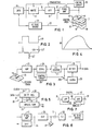
- a source of data signals 10 (FIGURE 1) supplies a bit stream to a write circuit 11 which converts the data bit stream from the usual NRZ representation to preferably an NRZI representation, such as signal llA.
- the signal to be recorded 11A (FIGURE 2) is supplied through a set of high pass filters HPF 12 which changes the signal waveform from 11A to a series of short duration pulses or spikes 12A. Each spike has a rapid rising edge followed by an exponential tail 12T which should have a duration no greater than a bit period of the NRZI signal llA.
- signal 12A travels through final amplifier 13 to a read/record transducer 14, for recording on a record medium 15.
- Record medium 15 consists of a flexible substrate 16 coated with a single magnetic layer 17.
- a lower portion 18 of the magnetic layer 17 contains a prerecorded control signal and an upper portion 19 of the layer 17 is used for recording the data signal 12A. It is preferred that the control signal in lower portion 18 be simultaneously sensed while recording the data signal from final amplifier 13 in upper portion 19.
- control circuit 20 is also connected to transducer 14.
- Control circuit 20 includes servo positioning apparatus responsive to the control signal to position transducer 14 with respect to medium 15 as well as deriving timing or clock signals for constant density recording.
- Transducer 14 is treated as a bilateral signal transfer device.
- the control signal in portion 18 has a low frequency characteristic whereas the data signal recorded in the upper portion 19 has a frequency characteristic exemplified by signal waveform 12A, and as shown generally in Figure 4A.
- AC bias source 21 supplies a single frequency sinusoid over lead 22 to final amplifier 13.
- AC bias source 21 has a frequency substantially higher than the higher frequencies of signal waveform 12A, such as from three to ten times data all I r s frequency. It has been found that the addition of the AC bias signal to the pulsed data signal enables repeated recording in upper portion 19 of magnetic layer 17 without deleterious effects on the control signal previously recorded in lower portion 18. Further, a data signal previously recorded in portion 19 can be overwritten without an intervening erasing step.
- the signal reproduction circuit illustrated in Fig. 3 is also directly connected to transducer 14.
- Preamplifier 25 supplies the sensed control signal to control circuit 20.
- the data signals are filtered out in control circuit 20 using conventional low pass filtering techniques.
- the sensed signal from preamplifier 25 is also supplied to equalizer circuit 26 for processing the recorded data signal 12A.
- a front end portion of the equalizer 26 includes a high pass filter (not shown in FIG. 2) for eliminating the control signal from the equalization and the data detection circuits.
- the high pass frequency filters in filter 12, as later described, and the high pass filter of equalizer 26 provide most of the compensation required for yielding an effective raised cosine recording channel. While some features of the channel response still need correction, the magnitude and duration are such that digital transversal techniques, as later described, can be used to accomplish the final tuning of the recording channel.
- equalizer 26 supplies its equalized signal to DC restore circuit 27, which in turn supplies its DC restored signal to detector 28 and to clock 29.
- DC restore circuit 27 in turn receives the output data signal for automatically adjusting its operation, as later fully described.
- equalizer 26 can be followed by a low pass or "roll off” filter, which reduces noise amplitudes above the needed data frequencies.
- FIGURES 5, 6 and 7 illustrate a preferred equalization scheme for the bias pulse write and read channels of FIGURES 1 and 3.
- the configuration of HPF 12 is shown in FIGURE 7 and comprises a digital transversal filter HPF 35, which supplies partially compensated signals to an analog filter HPF 36.
- HPF 36 in combination with a corresponding high pass filter in the front end portion of equalizer 26 completes most of the compensation.
- Digital transversal filter 35 receives the write data signal over lead 31 and the write data signal is then synchronously shifted through a multibit shift register 30 (FIGURE 5).
- a write clock which can be derived from control circuit 20 or can be independent, supplies timing signals over lead 34 to synchronously shift register 30.
- An analog sum circuit 33 receives the output signals from shift register 30 over leads 32 and provides an analog sum output over lead 48.
- Transversal filter 35 has four digit positions which respectively electrically control four driver transistors, schematically represented as single pole, single throw switches 40, 41, 42 and 43 (FIGURE 6). Leads 32 are connected to the base electrodes of the switch represented driver transistors. The emitters of the respective driver transistors are respectively connected via resistors 44, 45, 46 and 47 to ground reference potential.
- the transistor controlled by the bit position 2, transistor switch 42 is a write driver. That is, the resistive impedance of resistor 46 is less than the resistive impedances of resistors 44, 45 and 47. Therefore, it is considered as a "normal" write driver.
- the other three switches 40, 41 and 43 have effects on the output analog sum signal on lead 48 in accordance with the respective resistive impedances 44, 45 and 47 using known transversal filter technique selections.
- the data signal to be corrected has only simple overshoots. Therefore, only one polarity of correction is needed.
- Such a simple arrangement is made possible by employing DC restoration detection, together with the analog pulse write filters and the read filters to yield a raised cosine response at relatively low cost.
- control signal recorded in the lower portion 18 of magnetic layer 17 has a relatively low frequency compared with that of the recorded data signal 12A, it is relatively easy to filter the exact control signal frequency components from the data write current with tuned trap filters to reject data signal components at the control signal frequency. If the control signal is substantially a single frequency sinusoid, then filtering becomes still easier. While switching diodes or transistors can be used for isolation, it is desirable in a high quality recording system to eliminate the noise introduced by semiconductor switching devices. Since most of the recording energy is provided by the bias signal, the AC bias recording tends to reduce the writing voltage of the data signal 12A. Since the bias signal is a single frequency and is in general at least four times the data all 1's signal frequency, it is relatively easy to filter.
- amplifier 25 of the signal reproduction circuit can be effectively protected by a simple filtering circuit, such as shown in FIGURE 8.
- a lumped constant bandstop filter BSF 50 is tuned to resonance at the bias frequency of source 21, thus providing a very high series impedance at the bias frequency but a low impedance at the lower data frequencies.
- the lumped element BSF 50 can be of the L-type wherein a low shunt impedance at the bias frequency can be connected to the final amplifier 13 and preamplifier 25 side of BSF 50. This also provides a high impedance to ground at the lower data frequency.
- An electrical capacitor 51 having a high impedance to the data frequency but low impedance to the higher bias frequency can be inserted between transducer 14 and the AC bias source 21. While single-ended circuits are shown, it is to be understood that differential circuits may be employed with equal facility.
- a transmission line type filter TZ 52 may be interposed between capacitor 51 and AC bias source 21.
- the transmission line has an effective length of one-half the wavelength of the frequency of the bias frequency signal.
- the resonant impedance of transducer 14 and capacitor 51 can be exactly translated to an identical impedance seen by AC bias source 21. If the characteristic impedance of TZ 52 differs from that of the loads 14 and 51, some standing waves can occur.
- the lumped component filter 50, capacitor 51 and transmission line 52 can be on an arm supporting transducer 14. Additional components can be readily selected such that a resistive load impedance equal to the characteristic impedance of TZ 52 is achieved for eliminating standing waves. Then any electrical length of line can be employed.
- FIGURES 9 and 10 show two alternative arrangements for isolating the bias signal from the recording and signal reproducing circuits of FIGURES 1 and 3.
- transmission line TZ 53 has a quarter wavelength at the bias signal frequency. Accordingly, the low resonant impedance of LC circuit 54 is transformed into a high impedance at transducer 14.
- the arrangement of FIGURE 10 provides enhanced operation over that illustrated in FIGURE 9.
- the signal applied to pre-amplifier 25, the input amplifier, of the signal reproduction circuit of FIGURE 2 should be a sharp rise spike with a short exponential tail going to zero current within a bit period. Such a spike consists of very high frequency components which generally are higher than required for the bandwidth of read preamplifier 25.
- RC components 55 constitute high pass filter 36 of FIGURE 7.
- the resistive component of RC circuit 55 should equal the characteristic impedance of line TZ 53 for absorbing reflections. If a control signal circuit 20 is employed in connection with the FIGURE 10 arrangement, a low pass filter input to that circuit would normally be connected to junction 57, or at the input 58 to amplifier 25.
- FIGURE 11 illustrates a more complete system of filters and isolation circuits for using the bias pulse write technique of the present invention in combination with the control signal circuit 20.
- the transducer 14 has a centre tapped coil 14A having a centre tap connected to ground reference potential.
- Final amplifier 13 may be single-ended, but preamplifier 25 is preferably a differential or double- ended circuit.
- Servo filter 20A is a low-pass differentially- connected filter for supplying the control signal to circuit 20 of FIGURE 1.
- the components of FIGURE 11 correspond to those bearing the same reference numerals in FIGURE 10, except that a suffix A has been added to those circuits which have slight changes to accommodate the centre tap winding 14A of transducer 14, but which are readily understood from an inspection of Figure 10.
- the detection system employed with bias pulse write be a DC restoring detector.
- a DC restoring detector restores the eliminated DC and low frequency components to the signal being reproduced just prior to data detection.
- DC restoration includes sampling and holding the readback signal and timing operations such that the DC restorer reference is adapted with readback signal amplitude variations, including signal dropouts. This reference level is also a threshold level for data detection.
- a restoring detector regenerates the eliminated DC level and the low frequency components as if they had actually been transmitted, but without the noise components of the magnetic recording channel. Then, for faithful detection, equalizer 26 needs mainly to compensate for gap and separation losses, and to correct the phase characteristics of the readback signal.
- FIGURE 12 is a simplified diagram of a DC restorer and detector 27, 28.
- Full wave rectifier 60 full wave rectifies the equalized readback signal received from equalizer 26.
- Sample and hold circuit (S&H) 61 is timed by the output of data detector 28 for sampling the full wave rectified signal and using it to drive amplitude modulator 62.
- Modulator 62 receives the data signals from detector 28 to amplitude modulate the sampled and held readback signal in S&H 61.
- the amplitude modulated output of modulator 62 is a reference signal for compare circuit 63 of detector 28.
- Compare circuit 63 compares the received equalized signal with the reference signal for detecting it and supplies a timed detected control signal over line 64 as a data input to detector latch (D-type latch) 65.
- D-type latch detector latch
- Latch 65 is clocked at "C" by a usual phase lock loop oscillator (clock) which can be driven by the equalized readback signal or by the control signal read from the lower portion 18 of magnetic layer 17.
- the output of latch 65 is representative of the data signal carried by the readback signal.
- the line 64 signal can be used directly for controlling a clock or phase lock loop oscillator (not shown) which times the data detection of detector latch 65.
- Compare circuit 63 is merely a voltage threshold circuit.
- Monostable multivibrator 66 timed by detector latch 65, opens S and H circuit 61 to receive the full wave rectified signal from circuit 60 at a predetermined point within the bit cycle--i.e., when it is expected the peak of the readback signal will be occurring.
- Delay circuits can be included in S&H 61 for adjusting the sampling such that the peak of the full wave rectified signal is precisely timed to the timing of monostable circuit 66. Control of such circuits is well known.
- FIGURE 13 shows a complete readback system similar to FIGURE 3 but accents the analog gating usable in compare circuit 63.
- the output of the sample and hold circuit 61 (same circuit as in FIGURE 12) is applied to a pair of analog gates 70, 71, respectively, enabled by the output data value--i.e., whether it is a one or a zero.
- the gated sample and held full wave rectified signal then goes through differential amplifier 72 yielding a signal polarity in accordance with the value of the data output.
- the amplified signal is then low pass filtered by circuit LPF 73 for establishing a DC reference value for switching comparator- amplifier 74.
- the equalized readback signal from equalizer 26 is supplied to the signal input of switching comparator amplifier 74 to be amplitude threshold compared with the LPF 73 supplied DC reference signal.
- the threshold detected signal is then supplied to the data detector 28 which can be a latch, such as latch 65, in FIGURE 12.
- a single line 75 output from data detector 28A is shown.
- Inverter circuit 76 provides a binary output signal for controlling gate 70 as well as setting monostable multivibrator 66.
- the clocking circuits (which are of known design) are omitted from FIGURE 13.
- FIGURE 11 is a simplified version of the circuit of FIGURE 13 showing full wave rectifier 60 with sample and hold circuit 61 controlled by control circuit 20.
- Control circuit 20 is timed by the control signal read from the lower portion 18 of the magnetic layer 17 and supplied via amplifier 25.
- Amplitude modulator 62 is driven by the data and not data signal values from the data detector 28A.
- a simple differential amplifier 63A of the switching type provides amplitude threshold detection of the readback signal in a manner similar to the operation of amplifier 74.
- FIGURE 15 is a simplified diagram of a magnetic disk recording and reproducing system employing the invention.
- a rotating record storage disk 80 is positioned adjacent to radial transducer positioning carriage 81, which runs on radially aligned tracks 82 for positioning transducer 14 on one of a large plurality of concentric record tracks (not shown) on disk 80.
- Transducer 14 is suitably supported on carriage 81 via head support arm 83.
- Integrated circuits 84 immediately adjacent transducer 14 contain most of the components of the circuits previously described thus keeping to a minimum the lead length between the circuits and transducer 14. This is particularly important at the higher frequencies of operation because of parasitic capacitances.
- the mechanical dynamics of head arm 83 are easily adapted to accommodate the very slight mass addition of these circuits 84 to the free end of arm 83.
- the transmission lines previously referred to can be of a so-called printed circuit type as is well known in the art.
Landscapes
- Engineering & Computer Science (AREA)
- Signal Processing (AREA)
- Digital Magnetic Recording (AREA)
- Signal Processing For Digital Recording And Reproducing (AREA)
Applications Claiming Priority (2)
| Application Number | Priority Date | Filing Date | Title |
|---|---|---|---|
| US06/101,350 US4314289A (en) | 1979-12-07 | 1979-12-07 | Biased pulsed recording systems and methods |
| US101350 | 1979-12-07 |
Publications (2)
| Publication Number | Publication Date |
|---|---|
| EP0030300A1 true EP0030300A1 (fr) | 1981-06-17 |
| EP0030300B1 EP0030300B1 (fr) | 1984-03-21 |
Family
ID=22284180
Family Applications (1)
| Application Number | Title | Priority Date | Filing Date |
|---|---|---|---|
| EP80107233A Expired EP0030300B1 (fr) | 1979-12-07 | 1980-11-20 | Circuit pour un enregistreur de données magnétiques et procédé d'utilisation d'enregistreurs de données magnétiques |
Country Status (4)
| Country | Link |
|---|---|
| US (1) | US4314289A (fr) |
| EP (1) | EP0030300B1 (fr) |
| JP (1) | JPS5683820A (fr) |
| DE (1) | DE3067195D1 (fr) |
Cited By (1)
| Publication number | Priority date | Publication date | Assignee | Title |
|---|---|---|---|---|
| US4547818A (en) * | 1982-09-09 | 1985-10-15 | Tandberg Data A/S | Circuit arrangement for the recording of data on a magnetic recording carrier |
Families Citing this family (22)
| Publication number | Priority date | Publication date | Assignee | Title |
|---|---|---|---|---|
| US4371900A (en) * | 1981-01-23 | 1983-02-01 | Memorex Corporation | Equalization of DC null in reproducing a high density recording |
| US4346412A (en) * | 1981-04-21 | 1982-08-24 | Magnetic Peripherals, Inc. | Read signal processing circuit |
| US4480275A (en) * | 1982-04-02 | 1984-10-30 | Ampex Corporation | Constant current biased head driver |
| US4547817A (en) * | 1982-04-29 | 1985-10-15 | International Business Machines Corporation | High frequency magnetic recording method |
| US4510536A (en) * | 1982-07-16 | 1985-04-09 | Discovision Associates | Signal conditioning method and apparatus for FM code signal |
| GB8307428D0 (en) * | 1983-03-17 | 1983-04-27 | Aruga M | Recording and reconstructing digital data |
| JPS59207068A (ja) * | 1983-05-10 | 1984-11-24 | Panafacom Ltd | フロツピイデイスク装置 |
| US4564869A (en) * | 1983-11-21 | 1986-01-14 | Eastman Kodak Company | Zoned equalization for a magnetic disc |
| US4979051A (en) * | 1988-03-22 | 1990-12-18 | Eggebeen James A | Bimodal multi-track magnetic head |
| US4975791A (en) * | 1988-03-22 | 1990-12-04 | Carlisle Memory Products Group Incorporated | Recording system having head transducers with controlled skew |
| WO1991000594A1 (fr) * | 1989-06-30 | 1991-01-10 | Seagate Technology, Inc. | Procede de compensation des caracteristiques mecaniques et electriques uniques d'une unite de disques |
| DE3931828A1 (de) * | 1989-09-23 | 1991-04-04 | Krieg Gunther | Streifencode sowie verfahren und vorrichtung zum lesen eines solchen |
| US5341255A (en) * | 1990-10-17 | 1994-08-23 | Seagate Technology, Inc. | Disc drive head positioning servo system with coherent adjacent track magnetic patterns |
| US5319502A (en) * | 1992-01-10 | 1994-06-07 | International Business Machines Corporation | System and method for employing buried servos within a magnetic recording medium |
| US5287231A (en) * | 1992-10-06 | 1994-02-15 | Vtc Inc. | Write circuit having current mirrors between predriver and write driver circuits for maximum head voltage swing |
| US6456449B1 (en) | 1997-08-07 | 2002-09-24 | International Business Machines Corporation | Disk drive with wide servo burst pattern and wide servo sensing element |
| US6512647B1 (en) | 1999-08-27 | 2003-01-28 | Seagate Technology Llc | Method and apparatus for adaptive tuning bias current for magnetoresistive head |
| US7487908B1 (en) | 1999-10-23 | 2009-02-10 | Ultracard, Inc. | Article having an embedded accessible storage member, apparatus and method for using same |
| US8397998B1 (en) | 1999-10-23 | 2013-03-19 | Ultracard, Inc. | Data storage device, apparatus and method for using same |
| NL1015834C2 (nl) * | 2000-07-28 | 2002-01-29 | Onstream B V | Werkwijze voor het op verschillende diepte schrijven van informatie in een magnetische band. |
| US7133233B1 (en) * | 2000-10-24 | 2006-11-07 | Maxtor Corporation | Disk drive with read while write capability |
| US6882025B2 (en) * | 2003-04-25 | 2005-04-19 | Taiwan Semiconductor Manufacturing Company, Ltd. | Strained-channel transistor and methods of manufacture |
Citations (1)
| Publication number | Priority date | Publication date | Assignee | Title |
|---|---|---|---|---|
| US3614756A (en) * | 1970-01-21 | 1971-10-19 | Ibm | Magnetic record with servo track perpendicular to information track |
Family Cites Families (15)
| Publication number | Priority date | Publication date | Assignee | Title |
|---|---|---|---|---|
| US3032612A (en) * | 1957-09-25 | 1962-05-01 | Minnesota Mining & Mfg | Magnetic recording means |
| US3070670A (en) * | 1960-02-23 | 1962-12-25 | Ampex | Magnetic record head assembly |
| NL283021A (fr) * | 1961-09-11 | 1900-01-01 | ||
| BE640044A (fr) * | 1962-11-30 | 1964-03-16 | ||
| US3438018A (en) * | 1964-12-23 | 1969-04-08 | Ibm | Apparatus and method for magnetic recording |
| US3641524A (en) * | 1966-11-07 | 1972-02-08 | Leach Corp | Magnetic record and reproduce system for digital data having a nrzc format |
| GB1213169A (en) * | 1967-12-06 | 1970-11-18 | Int Computers Ltd | Improvements in or relating to methods of magnetic recording |
| US3838452A (en) * | 1972-12-07 | 1974-09-24 | Honeywell Inc | Recording amplifier for bias-type magnetic recording |
| US3864741A (en) * | 1973-06-28 | 1975-02-04 | Ibm | Servo channel equalization network |
| US3987488A (en) * | 1974-06-05 | 1976-10-19 | Matsushita Electric Industrial Co., Ltd. | Multi-tracks magnetic head with single turn winding structure |
| US3952329A (en) * | 1975-02-06 | 1976-04-20 | International Business Machines Corporation | Pulse compression recording |
| US3994016A (en) * | 1975-03-31 | 1976-11-23 | Honeywell Information Systems, Inc. | Head positioning servo system for disk drives |
| DE2735498A1 (de) * | 1977-08-06 | 1979-02-15 | Bosch Gmbh Robert | Schaltungsanordnung mit einem induktiven wandler |
| GB2013958B (en) * | 1977-12-27 | 1982-05-06 | Dolby Lab Licensing Corp | Analogue recording on magnetic media |
| US4202017A (en) * | 1978-05-08 | 1980-05-06 | Sperry Rand Corporation | Magnetic recording signal equalization apparatus |
-
1979
- 1979-12-07 US US06/101,350 patent/US4314289A/en not_active Expired - Lifetime
-
1980
- 1980-11-07 JP JP15601380A patent/JPS5683820A/ja active Granted
- 1980-11-20 DE DE8080107233T patent/DE3067195D1/de not_active Expired
- 1980-11-20 EP EP80107233A patent/EP0030300B1/fr not_active Expired
Patent Citations (1)
| Publication number | Priority date | Publication date | Assignee | Title |
|---|---|---|---|---|
| US3614756A (en) * | 1970-01-21 | 1971-10-19 | Ibm | Magnetic record with servo track perpendicular to information track |
Non-Patent Citations (2)
| Title |
|---|
| ELECTRONIC ENGINEERING, Vol. 51, No. 623, pages 61-67, May 1979 London, G.B. R. SILVER: "Magnetic tape recording and reproduction". * |
| NEC RESEARCH AND DEVELOPMENT, No. 35, October 1974, pages 37-45 Tokyo, JP. M. TACHIBANA et al.: "Equalization in digital recording". * |
Cited By (1)
| Publication number | Priority date | Publication date | Assignee | Title |
|---|---|---|---|---|
| US4547818A (en) * | 1982-09-09 | 1985-10-15 | Tandberg Data A/S | Circuit arrangement for the recording of data on a magnetic recording carrier |
Also Published As
| Publication number | Publication date |
|---|---|
| JPH0159667B2 (fr) | 1989-12-19 |
| DE3067195D1 (en) | 1984-04-26 |
| EP0030300B1 (fr) | 1984-03-21 |
| US4314289A (en) | 1982-02-02 |
| JPS5683820A (en) | 1981-07-08 |
Similar Documents
| Publication | Publication Date | Title |
|---|---|---|
| EP0030300B1 (fr) | Circuit pour un enregistreur de données magnétiques et procédé d'utilisation d'enregistreurs de données magnétiques | |
| EP0706173B1 (fr) | Optimisation de la précompensation de l'enregistrement dans un canal PRML | |
| US5691857A (en) | Method using matched filters for determining head positioner micro-jog in hard disk drive employing magneto-resistive heads | |
| US5576906A (en) | Synchronous detection of concurrent servo bursts for fine head position in disk drive | |
| US5862007A (en) | Method and apparatus for removing baseline shifts in a read signal using filters | |
| US5847890A (en) | Magnetic disk apparatus and a thermal asperity compensation method of the same | |
| JPS62110175A (ja) | 記録媒体の欠陥検出方法及び欠陥検出装置 | |
| JPS6049967B2 (ja) | 磁気記録方法及び装置 | |
| JPH0443349B2 (fr) | ||
| US6172832B1 (en) | Data storage system with improved biasing techniques for magneto-resistive element | |
| EP0581455A1 (fr) | Appareil de reproduction d'informations numériques | |
| US5319502A (en) | System and method for employing buried servos within a magnetic recording medium | |
| US6519106B1 (en) | Method and apparatus for correcting digital asymmetric read signals | |
| US5453888A (en) | Servo signal noise suppression in a sectored servo system by separating user data from servo data and filtering each with a specific filter | |
| Haynes | Magnetic recording techniques for buried servos | |
| JP2661064B2 (ja) | データ再生装置 | |
| US4542425A (en) | Apparatus for reading a record carrier | |
| JPS6353609B2 (fr) | ||
| YADA et al. | External clocking PRML magnetic recording channel for discrete track media | |
| Hopner | High-density binary recording using nonsaturation techniques | |
| JPS60124005A (ja) | 磁気抵抗効果型ヘツド再生回路 | |
| JPS6161220A (ja) | 磁気記録再生システム | |
| Roth | Improving Mass Storage Data Integrity | |
| JPH0581607A (ja) | 磁気記録装置 | |
| KR19980078179A (ko) | 피알엠엘검출방식을 채용한 자기디스크구동장치의 리드채널최적화를 위한 장치 및 방법 |
Legal Events
| Date | Code | Title | Description |
|---|---|---|---|
| PUAI | Public reference made under article 153(3) epc to a published international application that has entered the european phase |
Free format text: ORIGINAL CODE: 0009012 |
|
| AK | Designated contracting states |
Kind code of ref document: A1 Designated state(s): DE FR GB Designated state(s): DE FR GB |
|
| 17P | Request for examination filed |
Effective date: 19810706 |
|
| GRAA | (expected) grant |
Free format text: ORIGINAL CODE: 0009210 |
|
| AK | Designated contracting states |
Kind code of ref document: B1 Designated state(s): DE FR GB |
|
| REF | Corresponds to: |
Ref document number: 3067195 Country of ref document: DE Date of ref document: 19840426 |
|
| ET | Fr: translation filed | ||
| PLBE | No opposition filed within time limit |
Free format text: ORIGINAL CODE: 0009261 |
|
| STAA | Information on the status of an ep patent application or granted ep patent |
Free format text: STATUS: NO OPPOSITION FILED WITHIN TIME LIMIT |
|
| 26N | No opposition filed | ||
| PGFP | Annual fee paid to national office [announced via postgrant information from national office to epo] |
Ref country code: GB Payment date: 19901012 Year of fee payment: 11 |
|
| PGFP | Annual fee paid to national office [announced via postgrant information from national office to epo] |
Ref country code: FR Payment date: 19901020 Year of fee payment: 11 |
|
| PGFP | Annual fee paid to national office [announced via postgrant information from national office to epo] |
Ref country code: DE Payment date: 19901124 Year of fee payment: 11 |
|
| PG25 | Lapsed in a contracting state [announced via postgrant information from national office to epo] |
Ref country code: GB Effective date: 19911120 |
|
| GBPC | Gb: european patent ceased through non-payment of renewal fee | ||
| PG25 | Lapsed in a contracting state [announced via postgrant information from national office to epo] |
Ref country code: FR Effective date: 19920731 |
|
| PG25 | Lapsed in a contracting state [announced via postgrant information from national office to epo] |
Ref country code: DE Effective date: 19920801 |
|
| REG | Reference to a national code |
Ref country code: FR Ref legal event code: ST |