EP0581455A1 - Appareil de reproduction d'informations numériques - Google Patents
Appareil de reproduction d'informations numériques Download PDFInfo
- Publication number
- EP0581455A1 EP0581455A1 EP93305263A EP93305263A EP0581455A1 EP 0581455 A1 EP0581455 A1 EP 0581455A1 EP 93305263 A EP93305263 A EP 93305263A EP 93305263 A EP93305263 A EP 93305263A EP 0581455 A1 EP0581455 A1 EP 0581455A1
- Authority
- EP
- European Patent Office
- Prior art keywords
- signal
- circuit
- envelope
- time constant
- envelope detecting
- Prior art date
- Legal status (The legal status is an assumption and is not a legal conclusion. Google has not performed a legal analysis and makes no representation as to the accuracy of the status listed.)
- Granted
Links
Images


Classifications
-
- G—PHYSICS
- G11—INFORMATION STORAGE
- G11B—INFORMATION STORAGE BASED ON RELATIVE MOVEMENT BETWEEN RECORD CARRIER AND TRANSDUCER
- G11B20/00—Signal processing not specific to the method of recording or reproducing; Circuits therefor
- G11B20/10—Digital recording or reproducing
- G11B20/10009—Improvement or modification of read or write signals
Definitions
- the present invention relates to a digital information reproducing apparatus such as a magneto-optical disk reproducing apparatus.
- an amplitude detection or a peak detection is carried out for the purpose of converting a reproduction signal output from a reproduction head into a digital binary signal.
- the optical disk unit employs an amplitude detecting system or a peak detecting system according to a recording system of the digital data.
- the amplitude detecting system and the peak detecting system respectively correspond to an NRZI system and a RZ system.
- the information to be detected is a front edge and a rear edge of a recorded mark.
- the reproduction signal is converted into a digital signal by binary-comparing the reproduction signal with a proper threshold value.
- the center of a recorded mark is information to be detected. It is, therefore, necessary to differentiate the reproduction signal for seeking a zero cross point.
- This method is unable to separate a signal pulse for the center of the recorded mark from a noise pulse generated on the noise of the reproduction signal. Under this method, a data error is more likely to take place. To overcome this shortcoming, even in a peak detecting system, it is necessary to detect an amplitude for distinguishing the signal from the noise according to the amplitude of the reproduction signal.
- the reproduction signal converted into an electric signal through the effect of the reproduction head is amplified up to a proper amplitude level in an AC-coupled preamplifier 500 and then is guided to a low-pass filter 501.
- the low-pass filter 501 operates to remove unnecessary high-frequency components of the reproduction signal.
- the output of the low-pass filter 501 is guided to an equalizing circuit 502 for compensating for a restricted bandwidth caused according to resolution of the reproduction head.
- the output of the equalizing circuit 502 is guided to one input terminal of the comparator 503 and the first envelope detecting circuit 504 and the second envelope detecting circuit 505.
- a first envelope detecting circuit 504 is provided for detecting a positive side envelope of the output of the equalizing circuit 502 and is arranged to have a diode 610, a resistor 611, a capacitor 612 and a buffer 613.
- a second envelope detecting circuit 505 is provided for detecting a negative side envelope of the output of the equalizing circuit 502 and is arranged to have a diode 620, a resistor 621, a capacitor 622 and a buffer 623.
- the outputs of the envelope detecting circuits 504 and 505 are guided to an operating unit 506 in which the outputs are added to one signal and then the resulting signal is subject to filtering for removing a ripple.
- the output of the operating unit 506 is guided to the other input terminal of the comparator. According to the above arrangement, the reproduction signal is constantly controlled to keep the threshold value of the comparator for converting into a digital signal at the center of the reproduction signal according to the reproduction signal level.
- the envelope detecting circuit operates to follow even a disordered envelope of the reproduction signal caused by a minute defect on the recording medium. That is, the capacitors 612 and 622 store lots of charges corresponding to an amplitude of the reproduction signal obtained when the reproduction head passes along a minute defect. After it passes along the minute defect, the charges are discharged on the time constant defined by the combination of the capacitor 612 or 622 and the resistor 611 or 621. Hence, a considerably long time is taken in returning the storage into the storage amount of charges for the original amplitude of the reproduction signal. During this period, it is impossible to obtain a proper threshold value for the reproduction signal level, thereby bringing about a reproduction data error. That is, even a minute defect causes the reproduction data error to be like a burst, thereby disadvantageously lowering reliability of the data.
- a digital information reproducing apparatus comprising: readout means for reproducing information recorded on tracks of a recording medium by scanning a track of the recording medium; a first envelope detecting circuit providing a time constant circuit and for detecting an envelope of one polarity contained in a reproduction signal sent from the readout means; a second envelope detecting circuit providing a time constant circuit and for detecting an envelope of the other polarity contained in the reproduction signal; an adding circuit for obtaining a sum signal of outputs of the first and second envelope detecting circuits; a first comparator for comparing the reproduction signal with the sum signal; a subtracting circuit for obtaining a difference signal between the outputs of the first and second envelope detecting circuits; a second comparator for comparing the difference signal with a signal of a predetermined level; and a switching circuit for switching time constants of the time constant circuits provided in the first and second envelope detecting circuits, based on an output signal of the second comparator.
- the output of the second comparator is a signal corresponding to a disordered portion of a reproduction signal amplitude level (the disordered portion in which the amplitude level is largerthan the normally obtained reproduction signal amplitude level) caused by a minute defect.
- the switching circuit Based on the outputsignal of the second comparator, the switching circuit operates to reduce the time constant on which the charges stored in the capacitors of the first and the second envelope detecting circuits are discharged. After the reproduction head passes along the minute defective part, it takes a less time to return the storage amount of the charges into the charges for the original amplitude of the reproduction signal.
- a digital information reproducing apparatus comprising: readout means for reproducing information recorded on tracks of a recording medium by scanning a track of the recording medium; a first envelope detecting circuit providing a time constant circuit and for detecting an envelope of one polarity contained in a reproduction signal sent from the readout means; a second envelope detecting circuit providing a time constant circuit and for detecting an envelope of the other polarity contained in the reproduction signal; an adding circuit for obtaining a sum signal of outputs of the first and second envelope detecting circuits; a comparator for comparing the reproduction signal with the sum signal; a subtracting circuit for obtaining a difference signal between the outputs of the first and second envelope detecting circuits; a differentiating circuit for differentiating the difference signal; a switching circuit for switching time constants of the time constant circuits provided in the first and second envelope detecting circuits, based on an output signal of the differentiating circuit.
- the output of the differentiating circuit is a signal indicating an abrupt change of an amplitude level of the reproduction signal caused by a minute defect or the like.
- the switching circuit operates to reduce the time constant on which the charges stored in the capacitors of the first and the second envelope detecting circuits are discharged. After the reproduction head passes along the minute defective part, it takes a less time to return the storage amount of charges into the charges for the original amplitude of the reproduction signal.
- a digital information reproducing apparatus comprising: readout means for reproducing information recorded on tracks of a recording medium by scanning a track of the recording medium; a first envelope detecting circuit providing a time constant circuit and for detecting an envelope of one polarity contained in a reproduction signal sent from the readout means; a second envelope detecting circuit providing a time constant circuit and for detecting an envelope of the other polarity contained in the reproduction signal; an adding circuit for obtaining a sum signal of outputs of the first and second envelope detecting circuits; a first comparator for comparing the reproduction signal with the sum signal; a second comparator for comparing the sum signal with a signal of a predetermined level; and a switching circuit for switching time constants of the time constant circuits provided in the first and second envelope detecting circuits, based on an output signal of the second comparator.
- the output of the second comparator is a signal for a disordered portion (in which the amplitude level is larger than the normally obtained reproduction signal amplitude level) of an envelope of the reproduction signal caused by a minute defect or the like.
- the switching circuit Based on the output signal of the second comparator, the switching circuit operates to reduce a time constant on which the charges stored in the capacitors of the first and the second envelope detecting circuits are discharged. After the reproduction head passes along the minute defective part, it takes a less time to return the storage amount of charges into the charges for the original amplitude of the reproduction signal.
- a digital information reproducing apparatus comprising : readout means for reproducing information recorded on tracks of a recording medium by scanning a track of the recording medium; a first envelope detecting circuit providing a time constant circuit and for detecting an envelope of one polarity contained in a reproduction signal sent from the readout means; a second envelope detecting circuit providing a time constant circuit and for detecting an envelope of the other polarity contained in the reproduction signal; an adding circuit for obtaining a sum signal of outputs of the first and second envelope detecting circuits; a comparator for comparing the reproduction signal with the sum signal; a differentiating circuit for differentiating the sum signal; and a switching circuit for switching time constants of the time constant circuits provided in the first and second envelope detecting circuits, based on an output signal of the differentiating circuit.
- the output of the differentiating circuit is a signal indicating an abrupt change of an envelope of the reproduction signal caused by the minute defect or the like. Based on the output signal of this differentiating circuit, the switching circuit operates to reduce the time constant on which the charges stored in the capacitors of the first and the second envelope detecting circuits are discharged. After the reproduction head passes along the minute defective part, it takes a less time to return the storage amount of charges into the charges for the original amplitude of the reproduction signal.
- Fig. 1 is a block diagram showing an arrangement of a reproducing circuit of this invention.
- a reproduction signal converted into an electric signal by a reproduction head is amplified by an AC-coupled pre-amplifier 100 and then is guided to a low-pass filter 101.
- the output of the low-pass filter 101 is guided to an equalizing circuit 103 in which the waveform-equalizing treatment is carried out with respect to the output.
- the output of the equalizing circuit 102 is guided to one input terminal of a first comparator 103 as well as a first envelope detecting circuit 104 and a second envelope detecting circuit 105.
- the first envelope detecting circuit 104 for detecting an envelope on the positive side of the output of the equalizing circuit 102 is arranged of a diode 210, a resistor 211, a capacitor 212, an analog switch 213, a resistor 214 and a buffer amplifier 215.
- the second envelope detecting circuit 105 for detecting an envelope on the negative side of the output of the equalizing circuit 102 is arranged of a diode 220, a resistor 221, a capacitor 222, an analog switch 223, a resistor 224 and a buffer amplifier 225.
- the outputs of the first and the second envelope detecting circuits 104 and 105 are guided to an operating unit 106 in which these outputs are added.
- the added signal is filtered for removing a ripple.
- the output of the operating unit 106 is guided to the other input terminal of the comparator 103.
- the outputs of the envelope detecting circuits 104 and 105 are guided to an operating unit 107 in which a difference between these outputs are derived.
- the output of the operating unit 107 is guided to one input terminal of a second comparator 108.
- the other input terminal of the comparator is kept at a predetermined potential V b .
- the output of the comparator 108 is connected to the control input terminals of the analog switches 213 and 223.
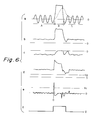
- a real line of Fig. 2a indicates an output signal of the equalizing circuit 102.
- the amplitude of the signal is amplified up to a proper level so that the high-pass noise components are removed from the signal through the effect of the pre-amplifier 100 at the previous stage, the low-pass filter 101 and the equalizing circuit 102. Further, the degrade of a frequency characteristic resulting from the reproduction head is compensated by these components.
- the periods A and C indicate normal states in which no disorder caused by a defect takes place in an envelope.
- the period B indicates a portion in which the amplitude of the reproduction signal is swung too much by means of a minute defect existing on the disk.
- the output signals of the first and the second envelope detecting circuits 104 and 105 for such a reproduction signal are indicated by Fig. 2b and Fig. 2c, respectively. Further, the output signal of the operating unit 107 is indicated by Fig. 2d and the output signal of the comparator 108 is indicated by Fig. 2e.
- Fig. 2a forthe portion A, the storage of charges in the capacitor 212 (222) of the envelope detecting circuit 104 (105) is performed by the diode 210 (220). The charges are discharged through the resistor211 (221). The time constant on which the charges are discharged is defined by the resistor 211 (221) and the capacitor 212 (222) and is normally set to a far larger value than the repeating period of the reproduction signal (output signals (b) and (c)).
- the output signal of the first envelope detecting circuit 104 abruptly rises.
- the output signal of the operating unit 107 is higher than the potential V b as shown by the output signal Fig. 2d (D of Fig. 2).
- the output signal of the comparator 108 is at high level. Since the output signal of the comparator 108 is at high level, the analog switches 213 and 223 are made closed and the charges stored in the capacitor 212 (222) are discharged through the resistors 211 and 214 (221 and 224).
- the time constant for this purpose is defined by (resistor 211) (resistor 214) / ⁇ (resistor 211) + (resistor 214) ⁇ ((resistor 221) (resistor 224) / ⁇ (resistor 221) + (resistor 224) ⁇ ) and the capacitor 212 (222).
- the time constant on which the charges are discharged from the capacitor 212 (222) when the analog switch 213 (223) is closed is sufficiently small and is substantially defined by the resistor 214 (224) and the capacitor 212 (222).
- the output signal of the first envelope detecting circuit 104 represents the envelope with fidelity during the period when successive minute defects appear as indicated in the output signals Fig. 2b and Fig. 2c.
- the output signal of the second envelope detecting circuit 105 is returned to a zero potential based on the time constant defined by the resistor 224 and the capacitor 222.
- the output signal of the operating unit 107 is as shown by the output signal Fig. 2d corresponding to the appearance of minute defects but keeps the potential V b or more.
- the output of he comparator 108 is maintained at high level (output signal (e)).
- the output signal of the first envelope detecting circuit 104 is started to return to the zero potential based on the time constant defined substantially by the resistor 214 and the capacitor 212.
- the output signal of the operating unit 107 lowers its signal level to the potential V b or less (E of Fig. 2).
- the output signal of the comparator 108 is at low level. Since the output signal of the comparator 108 is at low level, the analog switches 213 and 223 are made open and the normal circuit state takes place where the charges stored in the capacitor 212 (222) are discharged through the resistor 211 (221).
- the output signal of the operating unit 106 is as shown by a broken line of Fig. 2a and quickly follows the normal reproduction signal after the passage of the minute defective portion.
- Fig. 3 is a block diagram showing a reproducing circuit according to the second embodiment of the present invention.
- the same components as those shown in Fig. 1 have the same reference numbers.
- a pulse generating circuit 109 is newly provided for generating a control signal for opening or closing the analog switches 213 and 223.
- the concrete arrangement of the pulse generating circuit 109 has as a component a retriger-able and monostable multi-vibrator 300 which operates at the leading portion of the input signal as shown in Fig. 11.
- a real line indicated by Fig. 4a indicates the output signal of the equalizing circuit 102. This is true to the real line of Fig. 2a. With respect to this kind of reproduction signal, the output signals of the first and the second envelope detecting circuits 104 and 105 are indicated by Fig. 4b and Fig. 4c respectively. The output signal of the operating unit 107 is indicated by Fig. 4d and the output of the pulse generating circuit 109 is indicated by Fig. 4e.
- the output signal of the first envelope detecting circuit 104 indicates an abrupt rise.
- the output signal of the operating unit 107 is kept at the potential V b or more as indicated by Fig. 4d (D of Fig. 4).
- the output signal of the comparator 108 goes up to a high level so that the pulse generating circuit 109 may output a pulse signal having a predetermined time width (output signal (e)).
- the analog switches 213 and 223 are made closed so that the charges stored in the capacitor 212 (222) are discharged through the resistors 211 and 214 (221 and 224).
- the resistance of the resistor 124 (224) is set to a far smaller value than that of the resistor 211 (221), like the foregoing embodiment, the time constant on which the charges are discharged from the capacitor 212 (222) in the closed state of the analog switches 213 and 223.
- the output signal (b) of the first envelope detecting circuit 104 starts to return to a zero potential with a small time constant.
- the output signal (d) of the operating unit 107 lowers the signal level to the potential V b or less (E of Fig. 4). Then, while the output signal of the pulse generating circuit is kept at high level, the output signal of the operating unit 107 follows the reproduction signal.
- the analog switches 213 and 223 are made open, so that the overall circuit may enter into the normal state.
- the output signal of the operating unit 106 is as indicated by a broken line of Fig. 4a and swiftly follows the normal reproduction signal after the passage of a minute defective portion.
- Fig. 5 is a block diagram showing a reproducing circuit according to the third embodiment of the present invention.
- the same components as those shown in Figs. 1 and 3 have the same reference numbers.
- the output of the operating unit 107 for operating a difference between the outputs of the envelope detecting circuits 104 and 105 is guided to the differentiating circuit 110 in which the output is differentiated.
- the output signal of the differentiating circuit 110 is guided to one input terminal of the second comparator 111.
- the other input terminal of the comparator 111 is kept at the potential V c .
- the output signal of the comparator 111 is guided to the pulse generating circuit 112. Based on the output signal of the comparator 111, the pulse generating circuit 112 serves to generate a control signal for opening and closing the analog switches 213 and 223. The output of the pulse generating circuit 112 passes through a gate circuit 113 in order to control the analog switches 213 and 223.
- the pulse generating circuit 112 may be arranged of a retriger-able and monostable multi-vibrator, for example, like the foregoing embodiment.
- a circuit block 114 indicated by a broken line of Fig. 5 operates to generate a control signal for masking an output signal of the pulse generating circuit 112.
- a real line of Fig. 6a indicates an output signal of the equalizing circuit 102. This is true to Fig. 2a. With respect to the reproduction signal, the output signals of the first envelope detecting circuit 104 and the second envelope detecting circuit 105 are indicated by Fig. 6b and Fig. 6c, respectively. The output signal of the operating unit 107 is indicated by Fig. 6d and the output signal of the differentiating circuit 110 is indicated by Fig. 6e. Further, the output signal of the pulse generating circuit 112 is indicated by Fig. 6f.
- the output signal of the first envelope detecting circuit 104 indicates an abrupt rise. According to the abrupt rise, the output signal of the operating unit 107 rises (output signal (d)). Hence, the differentiating circuit 110 operates to output a pulsewise signal as corresponding to the abrupt rise of the output signal of the operating unit 107 as indicated by an output signal (Fig. 6e). The signal level of the pulsewise signal is maintained at the potential V c or more (D of Fig. 6). At this time, the output signal of the comparator 111 rises to a high level and the pulse generating circuit 112 serves to output a pulse signal having a predetermined time width (output signal (f)).
- the analog switches 213 and 223 are made closed so that the charges stored in the capacitor 212 (222) are discharged through the resistors 211 and 214 (221 and 224).
- the resistance of the resistor 214 (224) is set to a far smaller value than that of the resistor 211 (221)
- the time constant on which the charges of the capacitor 212 (222) are discharged in the closed state of the analog switches 213 and 223 is sufficiently small. This is the same as the foregoing embodiment.
- the output signal (b) of the first envelope detecting circuit 104 starts to return to a zero potential with a small time constant.
- the output signal (d) of the operating unit 107 lowers its signal level. Then, the output signal (d) of the operating unit 107 follows the reproduction signal while the output signal (f) of the pulse generating circuit 112 is kept at high level.
- the reproduction signal converted into an electric signal by the reproduction head is an intermittent signal in each block. If the reproduction signal is intermittent, at the head portion of the reproduction signal, the output signal (d) of the operating unit 107 abruptly rises so that the differentiating circuit 110 may output a pulsewise signal. If the output signal (e) of the differentiating circuit 110 goes up to a predetermined potential V c or higher, the output signal of the comparator 111 is shifted to a high level signal so that the pulse generating circuit 112 may output a pulse for closing the analog switches 213 and 223 even at the head portion of the reproduction signal.
- a circuit block 114 indicated by a broken line of Fig. 5 serves to generate a control signal for removing a pulse signal output by the pulse generating circuit 112 at the head portion of the reproduction signal if the reproduction signal is intermittent.
- a head position detecting circuit 230 and an inverter231 are provided for receiving the output signal (d) of the operating unit 107 as its input and sensing the head portion of the intermittent reproduction signal and generating a pulse having a predetermined time width.
- the outputsignal of the inverter231 is led to a gate circuit 113.
- the head position detecting circuit is, as shown in Fig.
- a comparator 310 for comparing the output of the operating unit 107 with the predetermined potential V d and a monostable multi-vibrator 311 for generating a pulse having a predetermined width of time when the output signal of the comparator 310 is shifted to a high level signal.
- the output signal of the operating unit 106 is indicated by a broken line of Fig. 6a. After the passage of a minute defective portion, the output signal swiftly follows the normal reproduction signal.
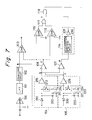
- Fig. 7 is a block diagram showing a reproducing circuit included in an optical disk reproducing apparatus to which the present invention applies.
- the same components as those shown in Figs. 1 and 5 have the same reference numbers.
- the output signal of the operating unit 106 is guided to one input terminals of the comparator 103 as well as to the comparators 115 and 116.
- the other input terminals of the comparators 115 and 116 are maintained at the potentials V e and -V e , respectively.
- the output signals of the comparators 115 and 116 are made logical OR in a gate circuit 117.
- the signal made logical OR passes to the analog switches 213 and 223 through a gate circuit 118forthe purpose of opening and closing those switches.
- a circuit block 114 indicated by a broken line of Fig. 7 operates to generate a control signal for masking the output signal of the gate circuit 117.
- the peak portion of the output signal of the operating unit 106 which is input to the comparator 103 is directly detected for opening or closing the analog switches 213 and 223.
- a real line indicated by Fig. 8a indicates an output signal of the equalizing circuit 102. This is the same as that shown in Fig. 2a. With respect to this kind of reproduction signal, the output signals of the first envelope detecting circuit 104 and the second envelope detecting circuit 105 are indicated by Fig. 8b and Fig. 8c, respectively. The output signals of the operating units 106 and 107 are indicated by Fig. 8d and Fig. 8e, respectively. The output signal of the gate circuit 117 is indicated by Fig. 8f.
- the output signal (b) of the first envelope detecting circuit 104 indicates an abrupt rise.
- the output signal (d) of the operating unit 106 becomes an potential V e or higher (D of Fig. 8).
- the output signal of the comparator 115 rises to a high level.
- the time constant on which the charges of the capacitor 212 (222) are discharged in the closed state of the analog switches 213 and 223 is made far smaller.
- the output signal (b) of the first envelope detecting circuit 104 is started to return to a zero potential on the time constant substantially defined by the resistor 214 and the capacitor 212.
- the output signal (d) of the operating unit 106 lowers its signal level to the potential V e or less (E of Fig. 8).
- the output signal of the comparator 115 indicates a low level. Since the output signal of the comparator 115 indicates the low level, the analog switches 213 and 223 are made open and the overall circuit enters into the normal state.
- the reproduction signal converted into an electric signal by the reproduction head is an intermittent signal in each block. If the reproduction signal is intermittent, at the head portion of the reproduction signal, a sag takes place because of the AC coupling at the first stage shown in Fig. 7. Hence, any one of the first envelope detecting circuit 104 and the second envelope detecting circuit 105 abruptly rises or falls and the output signal (d) of the operating unit 106 abruptly rises or falls accordingly.
- the circuit block 114 indicated by a broken line of Fig. 7 operates to generate a control signal for removing the pulse signal output from the gate circuit 117 in the head portion of the reproduction signal if the reproduction signal is intermittent.
- This embodiment has the circuit block 114 arranged like the embodiment shown in Fig. 5.
- the output signal of the operating unit 106 is indicated by a broken line of Fig. 8a. After the passage of a minute defective portion, the output signal swiftly follows the normal reproduction signal.
- Fig. 9 is a block diagram showing a reproducing circuit included in an optical disk reproducing apparatus to which the present invention applies.
- the output signal of the operating unit 106 is guided to one input terminals of the comparator 103 as well as the differentiating circuit 119 in which the signal is differentiated.
- the output signal of the differentiating circuit 119 are guided to one input terminal of the second comparators 120 and 121.
- the other input terminals of the comparators 121 and 121 are maintained at the potentials V f and -V f , respectively.
- the output signals of the comparators 120 and 121 are made logical OR in the gate circuit 122 and the signal made logical OR is guided to the pulse generating circuit 123.
- the output signal of the pulse generating circuit 123 is led to the analog switches 213 and 223 through a gate circuit 124 for the purpose of opening and closing the analog switches 213 and 223.
- the pulse generating circuit 123 may be arranged of a retriger-able and monostable multi-vibrator, for example, like the foregoing embodiment.
- Acir- cuit block 114 indicated by a broken line of Fig. 9 operates to generate a control signal for masking the output signal of the gate circuit 124.
- the differentiation of the output signal of the operating unit 106 stops the adverse effect of an envelope of the reproduction signal.
- a data train to be recorded is modulated by a modulator before recording it on an information track.
- the frequency band of the reproduction signal is limited so as to match to the frequency characteristic of the transmission path.
- This modulating system often includes relatively low frequency components.
- such low frequency components are removed by the AC coupling at the first stage of the reproducing system.
- the variation of an envelope (variation corresponding to the low frequency components of a bit train to be recorded) takes place.
- a real line shown by Fig. 10a indicates an output signal of the equalizing circuit 102. This is the same as that shown by Fig. 2a.
- the output signals of the first envelope detecting circuit 104 and the second envelope detecting circuit 105 are indicated by Fig. 10b and Fig. 10c, respectively.
- the output signal of the operating unit 106 is indicated by Fig. 10d and the output signal of the differentiating circuit 119 is indicated by Fig. 10e.
- the output signal of the gate circuit 122 is indicated by Fig. 10f and the output signal of the pulse generating circuit 123 is indicated by Fig. 10g.
- the output signal (b) of the first envelope detecting circuit 104 abruptly rises and the output signal (d) of the operating unit 106 rises accordingly.
- the output signal (e) of the differentiating circuit 119 changes according to the rise of the output signal of the operating unit 106 and keeps the signal level at the potential V f or higher (D of Fig. 10).
- the output signal of the comparator 120 rises to a high level so that the pulse generating circuit 123 may output a pulse signal (g) having a predetermined time width.
- the analog switches 213 and 223 are made closed so that the charges stored in the capacitor 212 (222) are discharged through the resistors 211 and 214 (221 and 224).
- the resistance of the resistor 214 (224) is set to a far smaller value than that of the resistor 211 (221), like the foregoing embodiment, the time constant on which the charges stored in the capacitor 212 (222) are discharged when the analog switches 213 and 223 are made closed becomes far smaller.
- the output signal of the first envelope detecting circuit 104 is started to return to a zero potential with a time constant substantially defined by the resistor 214 and the capacitor 212, resulting in lowering the signal level of the output signal of the operating unit 106 accordingly.
- the output signal (e) of the differentiating circuit 119 changes according to the fall of the output signal of the operating unit 106 and keeps its signal level at the potential -V f or less (E of Fig. 10).
- the output signal of the comparator 121 rises to a high level so that the pulse generating circuit 123 may be restarted (output signals (f) and (g)).
- circuit block 114 the arrangement and the operation of the circuit block 114 are the same as that of the foregoing embodiment.
- the output signal of the operating unit 106 is indicated by a broken line of the signal (Fig. 10a) and swiftly follows the normal reproduction signal after the passage of the minute defective portion.
- the present invention in a peak portion of the envelope caused by a defect or the like, by switching the time constant on which the charges stored in the capacitor of the envelope detecting cir- cuitare discharged, afterthe reproduction head passes the minute defective portion, it is possible to reduce the time taken in returning to the storage amount of charges corresponding to the amplitude of the original reproduction signal. Therefore, it is possible to prevent a burst-like data error from being caused by a minute defect.
- an intermittent reproduction signal is input to the AC-coupling reproducing system, it is easier to detect the peak portion of the envelope caused by the minute defect.
- the present invention it is possible to reduce the adverse effect given by the variation of an amplitude level of the reproduction signal caused by some factors such as variation between disks, environmental conditions like a temperature, and unevenness of the recording and reproducing characteristics of a disk and easier to detect the peak portion of the envelope caused by a minute defect.
Landscapes
- Engineering & Computer Science (AREA)
- Signal Processing (AREA)
- Signal Processing For Digital Recording And Reproducing (AREA)
Applications Claiming Priority (2)
| Application Number | Priority Date | Filing Date | Title |
|---|---|---|---|
| JP178135/92 | 1992-07-06 | ||
| JP4178135A JP2810592B2 (ja) | 1992-07-06 | 1992-07-06 | ディジタル情報再生装置 |
Publications (2)
| Publication Number | Publication Date |
|---|---|
| EP0581455A1 true EP0581455A1 (fr) | 1994-02-02 |
| EP0581455B1 EP0581455B1 (fr) | 1998-09-23 |
Family
ID=16043267
Family Applications (1)
| Application Number | Title | Priority Date | Filing Date |
|---|---|---|---|
| EP93305263A Expired - Lifetime EP0581455B1 (fr) | 1992-07-06 | 1993-07-05 | Appareil de reproduction d'informations numériques |
Country Status (4)
| Country | Link |
|---|---|
| US (1) | US5377054A (fr) |
| EP (1) | EP0581455B1 (fr) |
| JP (1) | JP2810592B2 (fr) |
| DE (1) | DE69321170T2 (fr) |
Cited By (4)
| Publication number | Priority date | Publication date | Assignee | Title |
|---|---|---|---|---|
| EP0709842A3 (fr) * | 1994-10-24 | 1997-01-02 | Sony Corp | Enregistrement et reproduction de données |
| EP1148682A3 (fr) * | 2000-04-17 | 2001-10-31 | Texas Instruments Incorporated | Séparateur adaptatif de données avec deux détecteurs de crêtes et un dispositif de calcul de moyenne pour obtenir le seuil optimal |
| EP0997901B1 (fr) * | 1998-10-27 | 2003-12-03 | Matsushita Electric Industrial Co., Ltd. | Appareil pour la mise en forme d'ondes et appareil pour traiter un signal de reproduction, utilisant ledit appareil |
| EP2296306A3 (fr) * | 2009-09-15 | 2012-03-28 | Yokogawa Electric Corporation | Dispositif de detection d'horloge |
Families Citing this family (14)
| Publication number | Priority date | Publication date | Assignee | Title |
|---|---|---|---|---|
| JPH0765503A (ja) * | 1993-08-25 | 1995-03-10 | Sharp Corp | 情報再生装置におけるアナログ/ディジタル変換回路 |
| JP3046515B2 (ja) * | 1994-12-16 | 2000-05-29 | シャープ株式会社 | 光情報記録再生装置の再生回路 |
| US5793240A (en) * | 1997-03-06 | 1998-08-11 | Texas Instruments Incorporated | Method and circuit for thermal asperity compensation in a data channel |
| TW408307B (en) * | 1997-12-15 | 2000-10-11 | Matsushita Electric Industrial Co Ltd | Method of processing optical signal and optical disk apparatus |
| US6189823B1 (en) | 1998-03-30 | 2001-02-20 | Daiwa Seiko, Inc. | Fishing reel having side plates efficiently attachable to and detachable from frames of reel body |
| KR100416594B1 (ko) * | 2001-04-11 | 2004-02-05 | 삼성전자주식회사 | 디스크 구동기에 있어서 알에프 신호의 슬라이스 및슬라이스 레벨 보상 장치와 그 방법 |
| US6882611B2 (en) * | 2002-06-04 | 2005-04-19 | Media Tek Inc. | Method and apparatus for defect detection in optical disc drives |
| KR100882376B1 (ko) | 2002-06-19 | 2009-02-05 | 브룩스 오토메이션, 인크. | 수직형 회전저장선반 및 오버헤드 호이스트의 조합에 기초한 반도체 제조용 자동식 재료 처리 시스템 |
| KR100880291B1 (ko) | 2002-10-11 | 2009-01-23 | 브룩스 오토메이션, 인크. | 자동 재료 핸들링 시스템 |
| US6914522B2 (en) * | 2003-05-23 | 2005-07-05 | Lear Corporation | Clamping circuit for an RF receiver system |
| JP2009076120A (ja) * | 2007-09-19 | 2009-04-09 | Panasonic Corp | 信号再生装置 |
| TWI361427B (en) * | 2007-11-23 | 2012-04-01 | Sunplus Technology Co Ltd | Apparatus and method for detecting a defect of an optical disc |
| JP7094690B2 (ja) | 2017-11-10 | 2022-07-04 | 株式会社シマノ | 両軸受リール |
| US11942951B2 (en) * | 2022-01-31 | 2024-03-26 | Dwellwell Analytics, Inc. | Conditional track and hold amplifier |
Citations (1)
| Publication number | Priority date | Publication date | Assignee | Title |
|---|---|---|---|---|
| GB2062421A (en) * | 1979-10-26 | 1981-05-20 | Sony Corp | Data extracting circuits; thresholding |
Family Cites Families (5)
| Publication number | Priority date | Publication date | Assignee | Title |
|---|---|---|---|---|
| JPS5846717A (ja) * | 1981-09-14 | 1983-03-18 | Nec Corp | パルス整形回路 |
| JPS59107410A (ja) * | 1982-12-08 | 1984-06-21 | Matsushita Electric Ind Co Ltd | デイジタル信号回路 |
| JPS59215040A (ja) * | 1983-05-20 | 1984-12-04 | Toshiba Corp | 画像情報円盤欠陥検出装置 |
| US4914398A (en) * | 1988-08-01 | 1990-04-03 | International Business Machines Corporation | Method and circuitry to suppress additive disturbances in data channels containing MR sensors |
| US5210518A (en) * | 1991-05-10 | 1993-05-11 | Echelon Corporation | Apparatus and method for reducing errors in data caused by noise |
-
1992
- 1992-07-06 JP JP4178135A patent/JP2810592B2/ja not_active Expired - Fee Related
-
1993
- 1993-07-02 US US08/086,625 patent/US5377054A/en not_active Expired - Lifetime
- 1993-07-05 DE DE69321170T patent/DE69321170T2/de not_active Expired - Lifetime
- 1993-07-05 EP EP93305263A patent/EP0581455B1/fr not_active Expired - Lifetime
Patent Citations (1)
| Publication number | Priority date | Publication date | Assignee | Title |
|---|---|---|---|---|
| GB2062421A (en) * | 1979-10-26 | 1981-05-20 | Sony Corp | Data extracting circuits; thresholding |
Non-Patent Citations (4)
| Title |
|---|
| PATENT ABSTRACTS OF JAPAN vol. 10, no. 206 (P-478)(2262) 18 July 1986 & JP-A-61 045 470 ( OLYMPUS OPTICAL CO LTD ) 5 March 1986 * |
| PATENT ABSTRACTS OF JAPAN vol. 11, no. 328 (P-629)27 October 1987 & JP-A-62 112 230 ( HITACHI LTD ) 23 May 1987 * |
| PATENT ABSTRACTS OF JAPAN vol. 12, no. 108 (E-597)7 April 1988 & JP-A-62 237 808 ( NISSAN MOTOR CO LTD ) 17 October 1987 * |
| PATENT ABSTRACTS OF JAPAN vol. 9, no. 129 (P-361)5 June 1985 & JP-A-60 013 362 ( MATSUSHITA DENKI SANGYO K.K. ) 23 January 1985 * |
Cited By (7)
| Publication number | Priority date | Publication date | Assignee | Title |
|---|---|---|---|---|
| EP0709842A3 (fr) * | 1994-10-24 | 1997-01-02 | Sony Corp | Enregistrement et reproduction de données |
| EP0997901B1 (fr) * | 1998-10-27 | 2003-12-03 | Matsushita Electric Industrial Co., Ltd. | Appareil pour la mise en forme d'ondes et appareil pour traiter un signal de reproduction, utilisant ledit appareil |
| US6798725B1 (en) | 1998-10-27 | 2004-09-28 | Matsushita Electric Industrial Co., Ltd. | Wave-shaping apparatus and reproduction signal processing apparatus including the same |
| EP1148682A3 (fr) * | 2000-04-17 | 2001-10-31 | Texas Instruments Incorporated | Séparateur adaptatif de données avec deux détecteurs de crêtes et un dispositif de calcul de moyenne pour obtenir le seuil optimal |
| US6735260B1 (en) | 2000-04-17 | 2004-05-11 | Texas Instruments Incorporated | Adaptive data slicer |
| EP2296306A3 (fr) * | 2009-09-15 | 2012-03-28 | Yokogawa Electric Corporation | Dispositif de detection d'horloge |
| US8531177B2 (en) | 2009-09-15 | 2013-09-10 | Yokogawa Electric Corporation | Timing detection device |
Also Published As
| Publication number | Publication date |
|---|---|
| JPH0620388A (ja) | 1994-01-28 |
| DE69321170D1 (de) | 1998-10-29 |
| DE69321170T2 (de) | 1999-04-15 |
| EP0581455B1 (fr) | 1998-09-23 |
| US5377054A (en) | 1994-12-27 |
| JP2810592B2 (ja) | 1998-10-15 |
Similar Documents
| Publication | Publication Date | Title |
|---|---|---|
| EP0581455B1 (fr) | Appareil de reproduction d'informations numériques | |
| EP0466329B1 (fr) | Appareil pour détecter des signaux de données digitales dans un signal analogique | |
| US4540897A (en) | Digital modulation signal reading device | |
| US4314289A (en) | Biased pulsed recording systems and methods | |
| EP0284279B2 (fr) | Circuit de détection des impulsions utilisant la qualification de l'amplitude et des temps | |
| KR900008413B1 (ko) | 레코드 캐리어로부터 판독된 정보 신호를 구형 신호로 변환시키는 회로장치 | |
| JPH07169064A (ja) | マルチビーム記録再生装置 | |
| CA1200598A (fr) | Appareil de lecture de signaux numeriques | |
| US5568465A (en) | Reading from record medium in either an inverted or non-inverted signal-processing mode | |
| JP2948016B2 (ja) | 情報記録再生方法 | |
| JPS6232547B2 (fr) | ||
| JP2000243032A (ja) | オフセットコントロール回路及びオフセットコントロール方法 | |
| JP2661064B2 (ja) | データ再生装置 | |
| JP3794275B2 (ja) | 光ディスク再生装置 | |
| NL8301645A (nl) | Digitaal signaalregistratie- en weergeefstelsel. | |
| EP1096488A2 (fr) | Appareil de traitement de signal de reproduction | |
| JPH03288331A (ja) | 光学的情報記録再生方法 | |
| JPS58114317A (ja) | デイジタル変調信号読取装置 | |
| KR200175746Y1 (ko) | 데이타 재생 장치 | |
| SU1068987A1 (ru) | Способ воспроизведени магнитной записи фазомодулированных сигналов | |
| JPH0777006B2 (ja) | 磁気再生装置 | |
| KR950004553B1 (ko) | 비디오 테이프의 재생 제어신호 재생 및 파형 변환장치 | |
| JPH07105116B2 (ja) | 記録媒体の再生装置 | |
| JPH0258733A (ja) | 光学式情報再生装置 | |
| JPS62110673A (ja) | 情報検出方法 |
Legal Events
| Date | Code | Title | Description |
|---|---|---|---|
| PUAI | Public reference made under article 153(3) epc to a published international application that has entered the european phase |
Free format text: ORIGINAL CODE: 0009012 |
|
| AK | Designated contracting states |
Kind code of ref document: A1 Designated state(s): DE FR GB NL |
|
| 17P | Request for examination filed |
Effective date: 19940418 |
|
| 17Q | First examination report despatched |
Effective date: 19961108 |
|
| GRAG | Despatch of communication of intention to grant |
Free format text: ORIGINAL CODE: EPIDOS AGRA |
|
| GRAG | Despatch of communication of intention to grant |
Free format text: ORIGINAL CODE: EPIDOS AGRA |
|
| GRAH | Despatch of communication of intention to grant a patent |
Free format text: ORIGINAL CODE: EPIDOS IGRA |
|
| GRAH | Despatch of communication of intention to grant a patent |
Free format text: ORIGINAL CODE: EPIDOS IGRA |
|
| GRAA | (expected) grant |
Free format text: ORIGINAL CODE: 0009210 |
|
| AK | Designated contracting states |
Kind code of ref document: B1 Designated state(s): DE FR GB NL |
|
| PG25 | Lapsed in a contracting state [announced via postgrant information from national office to epo] |
Ref country code: NL Free format text: LAPSE BECAUSE OF FAILURE TO SUBMIT A TRANSLATION OF THE DESCRIPTION OR TO PAY THE FEE WITHIN THE PRESCRIBED TIME-LIMIT Effective date: 19980923 |
|
| REF | Corresponds to: |
Ref document number: 69321170 Country of ref document: DE Date of ref document: 19981029 |
|
| ET | Fr: translation filed | ||
| NLV1 | Nl: lapsed or annulled due to failure to fulfill the requirements of art. 29p and 29m of the patents act | ||
| PLBE | No opposition filed within time limit |
Free format text: ORIGINAL CODE: 0009261 |
|
| STAA | Information on the status of an ep patent application or granted ep patent |
Free format text: STATUS: NO OPPOSITION FILED WITHIN TIME LIMIT |
|
| 26N | No opposition filed | ||
| REG | Reference to a national code |
Ref country code: GB Ref legal event code: IF02 |
|
| PGFP | Annual fee paid to national office [announced via postgrant information from national office to epo] |
Ref country code: GB Payment date: 20110629 Year of fee payment: 19 |
|
| PGFP | Annual fee paid to national office [announced via postgrant information from national office to epo] |
Ref country code: FR Payment date: 20110727 Year of fee payment: 19 |
|
| PGFP | Annual fee paid to national office [announced via postgrant information from national office to epo] |
Ref country code: DE Payment date: 20110629 Year of fee payment: 19 |
|
| GBPC | Gb: european patent ceased through non-payment of renewal fee |
Effective date: 20120705 |
|
| REG | Reference to a national code |
Ref country code: FR Ref legal event code: ST Effective date: 20130329 |
|
| PG25 | Lapsed in a contracting state [announced via postgrant information from national office to epo] |
Ref country code: GB Free format text: LAPSE BECAUSE OF NON-PAYMENT OF DUE FEES Effective date: 20120705 Ref country code: FR Free format text: LAPSE BECAUSE OF NON-PAYMENT OF DUE FEES Effective date: 20120731 Ref country code: DE Free format text: LAPSE BECAUSE OF NON-PAYMENT OF DUE FEES Effective date: 20130201 |
|
| REG | Reference to a national code |
Ref country code: DE Ref legal event code: R119 Ref document number: 69321170 Country of ref document: DE Effective date: 20130201 |