EP0030347A2 - Système et appareil d'exposition par faisceau électronique - Google Patents
Système et appareil d'exposition par faisceau électronique Download PDFInfo
- Publication number
- EP0030347A2 EP0030347A2 EP80107513A EP80107513A EP0030347A2 EP 0030347 A2 EP0030347 A2 EP 0030347A2 EP 80107513 A EP80107513 A EP 80107513A EP 80107513 A EP80107513 A EP 80107513A EP 0030347 A2 EP0030347 A2 EP 0030347A2
- Authority
- EP
- European Patent Office
- Prior art keywords
- electron beam
- deflection
- stage
- astigmatism
- correction
- Prior art date
- Legal status (The legal status is an assumption and is not a legal conclusion. Google has not performed a legal analysis and makes no representation as to the accuracy of the status listed.)
- Granted
Links
Images


Classifications
-
- H—ELECTRICITY
- H01—ELECTRIC ELEMENTS
- H01J—ELECTRIC DISCHARGE TUBES OR DISCHARGE LAMPS
- H01J37/00—Discharge tubes with provision for introducing objects or material to be exposed to the discharge, e.g. for the purpose of examination or processing thereof
- H01J37/30—Electron-beam or ion-beam tubes for localised treatment of objects
- H01J37/302—Controlling tubes by external information, e.g. program control
-
- H—ELECTRICITY
- H01—ELECTRIC ELEMENTS
- H01J—ELECTRIC DISCHARGE TUBES OR DISCHARGE LAMPS
- H01J37/00—Discharge tubes with provision for introducing objects or material to be exposed to the discharge, e.g. for the purpose of examination or processing thereof
- H01J37/02—Details
- H01J37/04—Arrangements of electrodes and associated parts for generating or controlling the discharge, e.g. electron-optical arrangement or ion-optical arrangement
- H01J37/147—Arrangements for directing or deflecting the discharge along a desired path
- H01J37/1472—Deflecting along given lines
- H01J37/1474—Scanning means
- H01J37/1475—Scanning means magnetic
-
- H—ELECTRICITY
- H01—ELECTRIC ELEMENTS
- H01J—ELECTRIC DISCHARGE TUBES OR DISCHARGE LAMPS
- H01J37/00—Discharge tubes with provision for introducing objects or material to be exposed to the discharge, e.g. for the purpose of examination or processing thereof
- H01J37/02—Details
- H01J37/04—Arrangements of electrodes and associated parts for generating or controlling the discharge, e.g. electron-optical arrangement or ion-optical arrangement
- H01J37/153—Electron-optical or ion-optical arrangements for the correction of image defects, e.g. stigmators
-
- H—ELECTRICITY
- H01—ELECTRIC ELEMENTS
- H01J—ELECTRIC DISCHARGE TUBES OR DISCHARGE LAMPS
- H01J37/00—Discharge tubes with provision for introducing objects or material to be exposed to the discharge, e.g. for the purpose of examination or processing thereof
- H01J37/30—Electron-beam or ion-beam tubes for localised treatment of objects
- H01J37/304—Controlling tubes by information coming from the objects or from the beam, e.g. correction signals
Definitions
- the present invention relates to an electron beam exposure system, in which an electron beam is radiated to a medium placed on a continuously moving stage, and an apparatus for exposing a medium by continuously moving the stage supporting said medium.
- the electron beam exposure system is well known as a method for forming minute patterns of an LSI (Large Scale Integrated Circuit).
- This electron beam exposure system is classified into the step and repeat system where patterns are depicted on the wafer by repeating a process that a wafer is exposed to, for example, the variable rectangular beam, then shifted by one step and then exposed to said beam by shifting the stage mounting said wafers step by step, and the continuous stage moving system where patterns are depicted by projecting the beam to the wafers while said stage is always moved continuously.
- the electron beam deflection range is comparatively as wide as 2(two) to 5(five) mm square, and the stage moves 2 to 5 mm in a direction and stops to project the electron beam on a wafer and then moves 2 to 5 mm after the projection.
- the exposed portions are thus sequentially formed by repeating such operations.
- the stage moves continuously at a rate of about 20mm/sec, the beam is scanned in the range as narrow as about 250 um at a right angle to the moving direction of the wafer, and thereby patterns are depicted on the wafers.
- the former step and repeat system has such a merit that the beam position control is easy at the time of depicting patterns since the stage is in the stationary condition, but also has such a demerit that compensation for obscurity such as distortion, field curvature, astigmatism etc. is required since the deflection width of electron beam is wide and the movement of stage lacks smoothness because it is moved step by step for every pattern depiction and always subjected to acceleration and deceleration.
- the latter continuous stage moving system has such a merit that the stage moves smoothly and naturally on account of the continuous movement of the stage and variety of compensations mentioned above are not required due to narrow deflection of the electron beam, but also has such a demerit that the beam position control is complicated due to the continuous movement of stage, a narrow deflection of electron beam provides less amount of exposing process, and thereby a longer period is required for depicting desired patterns.
- an electron beam exposure system in which an electron beam is radiated to a medium mounted on a continuously moving stage characterized in that a correction memory is provided for storing electron beam correction data for a least one of a field curvature, an astigmatism and a distortion which change in accordance with deflection amount of electron beam wherein said deflection amount is obtained from a difference between a medium position data and a beam deflection position data from a processor, and said electron beam correction data corresponding to said deflection amount is read out from said correction memory and applied to a beam control means.
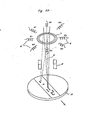
- FIG. 1 and Figure 2 respectively show the embodiment of the electron beam exposure apparatus of the present invention.
- G is an electron gun and B is the electron beam emitted from said electron gun.
- 1 is a first slit for the electron beam B.
- 2 designates deflection plates for deflecting the electron beam section into a variable rectangular shape, 3 a second slit, 4 electron lenses for focusing and image forming and 5 deflection plates for correcting distortion.
- 6 is a stigmator coil
- 7 is a focus coil
- 8 is a deflection coil
- 9 is a convergence coil
- 10 is a medium such as a wafer placed on a stage 11 which moves continuously.
- the electron beam B emitted from the electron gun G is converged by the electron lens 4 whereby an image of the first slit 1 is formed on the second slit 3 and deflected by the deflection plate 2.
- the portion Ba indicated by the mesh of Fig. 3 of the electron beam B passes the aperture 3a of the second slit 3 and shaped into the rectangular beam, and projected to the desired position on the wafer 10 via the electron lens, convergence coil and deflection coil etc.
- the semiconductor wafer 10 allows, as indicated in Fig. 4, formation of many integrated circuit chips 10a, 10b,.... (these are scribed into individual IC chips) and usually respective chips have the same patterns, namely the same internal element arrangement.
- each pattern of the integrated circuit chip is depicted by the procedures indicated in Fig. 5, namely a desired pattern is depicted in unit of individual rectangular patterns B1, B2, B3, across and by adequately combining them, namely the exposing of the photoresist is performed.
- the exposing location on the wafer is shifted in the present invention by the movement of stage 11 and beam deflection by the deflection coil 8.
- a computer.12 used for such control. 13 is a memory for storing pattern data of said integrated circuit chips.
- 14 is a register which stores data of the field coordinates of the chips on the wafer;
- 15 is an adder for adding a readout signal S 1 from the memory 13 and the signal S 2 which means the field coordinate 14 and thereby outputs a combined signal S 3 ;
- 16 is a dynamic correction memory which stores correction data for correcting the field curvature, the astigmatism and the distortion of the electron beam.
- the field coordinates are represented by the specific points of chips on the wafer, for example, by the coordinates of the points P1, P2,.... and the signal S 3 obtained by adding such field coordinate signal and the output signal S1 of the memory 13 indicated the coordinates of individual IC patterns on the wafer.
- the stage 11 is driven in the X and Y directions by a motor, not illustrated, and the locations of X and Y, more specifically., the locations of the field coordinates X, Y of wafer on said stage are measured by the laser interferometer 17.
- the wafer 10 is not always placed on the stage 11 in the determined condition and usually it is deviated or rotated by a certain angle to the X and Y directions from the determined condition.
- 18 is a primary converter consisting of the matrix circuit (which performs addition/subtraction and multipli- cation/division) in order to correct such positional deviation.
- positions of three marks determining the plane of wafer are detected by the electron beams, deviation from the determined position is detected by measuring such positions, an output of the laser interferometer 17 is corrected in accordance with such deviation and said output is set to the coordinates predetermined by the memory 13 and the register 14.
- 19 is a subtractor which outputs a difference signal S 6 obtained by subtracting the signal S 5 of the converter 18 from the signal S 3 of said adder 15.
- the output signal S 6 of the subtractor 19 is added to the amplifier 24 via the primary converter 18.
- the amplifier 24 converts the digital signal S 6 to the analog signal S10 and amplifies said signal in order to excite the deflection coil 8.
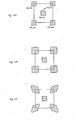
- the pattern is actually not only obscured but also deformed as the electron beam is deflected as indicated in Fig. 6C. This is called the astigmatism.
- the correct pattern can be depicted as indicated in Fig. 6A by correcting astigmatism for the pattern of Fig. 6C to the pattern of Fig. 6B and by correcting the field curvature.
- the pattern is depicted at the correct position like the patterns P 1 , P 2 , P 3 , P 4 on the diagonal of the square with the center P O .
- the pattern P O of the position (x m , y O ) namely even when the information to deflect the pattern P 0 to the position (x m , y O ) is input to the column from the CPU, the electron beam is actually deflected to the position (x , y O ) and the pattern P O is depicted.
- Such deviation of the deflection position is called the distortion.
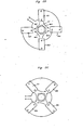
- the focus coil 7 used for correcting the abovementioned field curvature is a ringshape coil wound in such a way as surrounding the electron beam B as indicated in Fig. 2A.
- the stigmator coil 6 used for correcting astigmatism consists of eight (8) solenoid coils a 1 ,... .,a4 and b 1 ,...., b 4 which are arranged in the same plane with an interval of 45 degrees.
- FIGS 2B, 2C show the coils in the form of block and also indicate mutual connections.
- the coils a 1 ,...., a 4 have the same number of turns, but are connected in series so that the backward winding appears in every another coil. Therefore, when a current is applied to each coil via the winding, the pole N appears in the space side surrounded by the coils in the case of coils a 1 and a 3 , and the pole S appears in the case of the coil a 2 and a4. Thereby, as indicated in the figure, the magnetic lines of force m 1 , m 2 , m 31 m 4 appear.
- the circular beam Ci can be deformed vertically or horizontally as indicated by the dotted line by controlling a current flowing through the coils.
- the ellipse beam indicated by the dotted line can be shaped to the circular beam C.
- the coils b 1 ,....,b 4 indicated in Fig. 2C have the same structure as the coils a 1 ,....,a 4 indicated in Fig. 2B and they are arranged with displacement of only 45 degrees.
- the electron beam can be shaped into the direction displaced only by 45 degrees from that in the Fig. 2B.
- the electron beam can be shaped freely by arranging the coils of Fig. 2B, 2C through the combination as indicated in Fig. 2A.
- distortion changes depending on the deflection angle, but is also influenced by the correction of the field curvature and the astigmatism. Therefore, distortion can be understood as the function of beam deflection angle ⁇ and said field curvature and astigmatism.
- correction data of said values for respective deflection angles are written into the memory 16. 21 to 23 are amplifiers for activating the deflection plates 5, stigmator coil 6, focus coil 7 through DA conversion of the output of said memory.
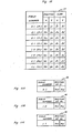
- Figure 7 shows content of the memory 16.
- the one region to be exposed by the electron beam is divided into j sections in the direction X and i sections in the direction Y (i, j are integers).
- the region to be exposed can be considered as the minute regions divided having the addresses from (ax 1 , aY 1 )to(axj, ayi).
- the correction amount of the field curvature at the address (ax 1 , ay 1 ) is pre-obtained as f 1
- correction amount of the astigmatism in the direction X as Sx 1 and that in the direction Y as Sy l is obtained previous to the exposure in the same way, and moreover each correction amount is stored in the memory 16.
- This address corresponds to the deflection amount of the electron beam as will be explained later.
- Figure 8 shows the plan view of the wafer 10 placed on the stage 11.
- the mirrors 81, 82 are respectively provided at the sides in the directions of X and Y of the stage 11, and the laser interferometer 17X for detecting the position in the direction X of the stage 11 and the laser interferometer 17Y for detecting the position in the direction Y of the stage 11 are provided.
- the stage 11 is continuously moved in the directions X and Y with a motor not illustrated, and thereby the region on the wafer 10 is sequentially and continuously exposed as a result of relative operations as indicated by the arrow 83.
- Figure 9 shows an enlarged portion of the wafer 10.
- the chips in size of lx x ly are arranged in the form of matrix on the wafer 10 and the one chip consists of the three exposing fields F 1 , F 2 and F 3 , each is in size of 1 x x l f .
- the size of 1 is a little smaller than the deflection width of electron beam.
- the patterns Q 1 , Q 2 , Q 3 , Q 4 are to be exposed, while Q 5 and Q 6 in the field F 2 , and Q 7 and Q 8 in the field F 3 are to be exposed.
- the origins of the fields F 1 , F 2 and F 3 are respectively indicated by O 1 , 0 2 and 0 3 .
- the coordinate of origin of each field is transferred to the register 14 from the CPU 12 in accordance 'with the fields F 1 , F 2 , F 3 and stored therein.
- the data x 1 , y 1 and 1 1 and 1 1 are read out from the pattern memory 13, while the data O 1x , O 1y are obtained from the register 14. Then, these are added in the adder 15. Thereby, the deflection amount from the origin of exposure by means of the electron beam can be obtained, if the stage is not moved.
- the output signal S 3 in Fig. 1 indicates the coordinates of pattern in the relevant chip (the chip specified by the field coordinate 14 - viewed from the field coordinate of eht wafer 10.
- the laser interferometer 17 provides the current position signal S4 of the wafer 10.
- the signal is substracted from the signal S 3 by the subtractor 19, the difference output signal of the subtractor 19 ist corrected by the primary converter 18, and the output S 6 indicates the amount of deflection of electron beam.
- the deflection coil 8 is activated in accordance with such signal S 6 and therefore the beam is projected to the desired position in accordance with the data of pattern coordinate.
- the stage moves but since the rectangular beam projection period is very short, the wafer is considered to be in the stationary condition during projection of electron beam.
- the difference signal S 6 is also used for retrieval of memory 16, and the correction amount f, S , S , d x , d y of the field curva- ture, astigmatism and distortion corresponding to the deflection amount of the electron beam are read out and then applied to the respective adjusting means 5, 6, 7 via the amplifiers 21 to 23.
- the deflection amounts X, Y are obtained by the following equation.
- (x 1 , y 1 ) is the coordinate of the pattern Q 1 from the origin 0 1
- (X p , Y ) is the coordinate of the origin 0 1
- (X(t), Y(t)) is the output of the laser interferometer, namely the positional coordinate of the stage.
- Above primary conversion is carried out by the primary converter 18 of Figure 1.
- the electron beam exposure system and the apparatus for the same have offered a variety of effects such as a high speed formation of pattern and accurate depiction of patterns since the stage is moved continuously and the rectangular electron beam is projected with deflection by a large deflection angle.
Landscapes
- Chemical & Material Sciences (AREA)
- Analytical Chemistry (AREA)
- Electron Beam Exposure (AREA)
Applications Claiming Priority (2)
| Application Number | Priority Date | Filing Date | Title |
|---|---|---|---|
| JP15992079A JPS5693318A (en) | 1979-12-10 | 1979-12-10 | Electron beam exposure device |
| JP159920/79 | 1979-12-10 |
Publications (3)
| Publication Number | Publication Date |
|---|---|
| EP0030347A2 true EP0030347A2 (fr) | 1981-06-17 |
| EP0030347A3 EP0030347A3 (en) | 1982-03-03 |
| EP0030347B1 EP0030347B1 (fr) | 1987-04-01 |
Family
ID=15704035
Family Applications (1)
| Application Number | Title | Priority Date | Filing Date |
|---|---|---|---|
| EP80107513A Expired EP0030347B1 (fr) | 1979-12-10 | 1980-12-02 | Système et appareil d'exposition par faisceau électronique |
Country Status (4)
| Country | Link |
|---|---|
| US (1) | US4362942A (fr) |
| EP (1) | EP0030347B1 (fr) |
| JP (1) | JPS5693318A (fr) |
| DE (1) | DE3071944D1 (fr) |
Cited By (9)
| Publication number | Priority date | Publication date | Assignee | Title |
|---|---|---|---|---|
| GB2123582A (en) * | 1982-06-18 | 1984-02-01 | Nat Res Dev | Correction of astigmatism in electron beam instruments |
| EP0115952A1 (fr) * | 1983-01-31 | 1984-08-15 | Fujitsu Limited | Procédé et appareil d'exposition à un faisceau d'électrons |
| US4567369A (en) * | 1982-06-18 | 1986-01-28 | National Research Development Corporation | Correction of astigmatism in electron beam instruments |
| FR2568720A1 (fr) * | 1984-08-04 | 1986-02-07 | Leybold Heraeus Gmbh & Co Kg | Procede et dispositif de commande de l'etat de focalisation d'un faisceau d'electrons devie |
| EP0105694A3 (en) * | 1982-09-30 | 1986-08-06 | Kabushiki Kaisha Toshiba | Charged particle beam exposure apparatus |
| EP0148784A3 (en) * | 1984-01-10 | 1987-04-08 | Fujitsu Limited | Calibration of electron beam apparatus |
| EP0222219A3 (en) * | 1985-11-02 | 1989-01-11 | Leybold Aktiengesellschaft | Device for the bombardment of a medium with an electron beam |
| EP0418894A3 (en) * | 1989-09-20 | 1992-01-02 | Matsushita Electric Industrial Co., Ltd | A scanning electron microscope and a method of displaying cross sectional profiles using the same |
| US5550836A (en) * | 1992-11-06 | 1996-08-27 | Hewlett-Packard Company | High speed data transfer over twisted pair cabling |
Families Citing this family (26)
| Publication number | Priority date | Publication date | Assignee | Title |
|---|---|---|---|---|
| US4424450A (en) | 1981-09-08 | 1984-01-03 | Varian Associates, Inc. | Hybrid moving stage and rastered electron beam lithography system employing approximate correction circuit |
| JPS58121625A (ja) * | 1981-12-28 | 1983-07-20 | Fujitsu Ltd | 電子ビ−ム露光装置 |
| JPS58218117A (ja) * | 1982-06-11 | 1983-12-19 | Fujitsu Ltd | 電子ビ−ム制御装置 |
| JPS59124719A (ja) * | 1982-12-29 | 1984-07-18 | Fujitsu Ltd | 電子ビ−ム露光装置 |
| AT388628B (de) * | 1986-01-31 | 1989-08-10 | Ims Ionen Mikrofab Syst | Einrichtung fuer projektionsgeraete |
| JPS60231324A (ja) * | 1984-04-28 | 1985-11-16 | Fujitsu Ltd | 電子ビ−ム露光装置 |
| FR2597259A1 (fr) * | 1986-04-15 | 1987-10-16 | Thomson Csf | Dispositif a faisceau electronique pour projeter l'image d'un objet sur un echantillon |
| FR2605143B1 (fr) * | 1986-10-14 | 1994-04-29 | Thomson Csf | Dispositif d'optique electronique, d'illumination et de limitation d'ouverture variables, et son application a un systeme de lithographie par faisceau d'electrons |
| DE8634545U1 (de) * | 1986-12-23 | 1987-05-21 | Siemens AG, 1000 Berlin und 8000 München | Korpuskularstrahlgerät zur fehlerarmen Abbildung linienförmiger Objekte |
| AT393925B (de) * | 1987-06-02 | 1992-01-10 | Ims Ionen Mikrofab Syst | Anordnung zur durchfuehrung eines verfahrens zum positionieren der abbildung der auf einer maske befindlichen struktur auf ein substrat, und verfahren zum ausrichten von auf einer maske angeordneten markierungen auf markierungen, die auf einem traeger angeordnet sind |
| JPH0628232B2 (ja) * | 1987-09-16 | 1994-04-13 | 富士通株式会社 | 荷電ビーム露光装置 |
| JP2614884B2 (ja) * | 1988-02-04 | 1997-05-28 | 富士通株式会社 | 電子ビーム露光方法及びその装置 |
| KR920000941B1 (ko) * | 1988-02-16 | 1992-01-31 | 후지쓰 가부시끼가이샤 | 전자빔 노광장치 |
| JPH0744143B2 (ja) * | 1988-09-20 | 1995-05-15 | 株式会社日立製作所 | 電子線描画装置の外部磁気補正方法 |
| JP2835097B2 (ja) * | 1989-09-21 | 1998-12-14 | 株式会社東芝 | 荷電ビームの非点収差補正方法 |
| JP3148353B2 (ja) * | 1991-05-30 | 2001-03-19 | ケーエルエー・インストルメンツ・コーポレーション | 電子ビーム検査方法とそのシステム |
| US5329130A (en) * | 1991-08-06 | 1994-07-12 | Fujitsu Limited | Charged particle beam exposure method and apparatus |
| US5391886A (en) * | 1991-08-09 | 1995-02-21 | Fujitsu Limited | Charged particle beam exposure system and method of exposing a pattern on an object by such a charged particle beam exposure system |
| US5304811A (en) * | 1991-08-09 | 1994-04-19 | Fujitsu Ltd. | Lithography system using charged-particle beam and method of using the same |
| US5285074A (en) * | 1992-06-03 | 1994-02-08 | International Business Machines Corporation | Dynamic compensation of non-linear electron beam landing angle in variable axis lenses |
| US5663568A (en) * | 1995-10-20 | 1997-09-02 | Lucent Technologies Inc. | Apparatus for controlling a charged particle beam and a lithographic process in which the apparatus is used |
| JP3455006B2 (ja) * | 1996-03-25 | 2003-10-06 | 株式会社東芝 | 荷電粒子ビーム装置 |
| JP4410871B2 (ja) * | 1999-03-25 | 2010-02-03 | キヤノン株式会社 | 荷電粒子線露光装置及び該装置を用いたデバイス製造方法 |
| US7119351B2 (en) | 2002-05-17 | 2006-10-10 | Gsi Group Corporation | Method and system for machine vision-based feature detection and mark verification in a workpiece or wafer marking system |
| DE102012004134A1 (de) | 2012-02-29 | 2013-08-29 | Volkswagen Aktiengesellschaft | Bordnetz und Verfahren zur gezielten Erwärmung eines Energiespeichers in einem Bordnetz |
| DE102013226372A1 (de) | 2013-12-18 | 2015-06-18 | Volkswagen Aktiengesellschaft | Batterieeinheit und Verfahren zum Heizen einer Batterieeinheit |
Family Cites Families (8)
| Publication number | Priority date | Publication date | Assignee | Title |
|---|---|---|---|---|
| GB1325540A (en) * | 1969-10-10 | 1973-08-01 | Texas Instruments Ltd | Electron beam apparatus |
| US3699304A (en) * | 1969-12-15 | 1972-10-17 | Ibm | Electron beam deflection control method and apparatus |
| US3922546A (en) * | 1972-04-14 | 1975-11-25 | Radiant Energy Systems | Electron beam pattern generator |
| US4066863A (en) * | 1974-06-26 | 1978-01-03 | International Business Machines Corporation | Method and system for automatically correcting aberrations of a beam of charged particles |
| US4075488A (en) * | 1974-09-06 | 1978-02-21 | Agency Of Industrial Science & Technology | Pattern forming apparatus using quadrupole lenses |
| JPS5283177A (en) * | 1975-12-31 | 1977-07-11 | Fujitsu Ltd | Electron beam exposure device |
| JPS5333473A (en) * | 1976-09-09 | 1978-03-29 | Kubota Ltd | Electric dust collector |
| US4180738A (en) * | 1977-07-30 | 1979-12-25 | National Research Development Corporation | Astigmatism in electron beam probe instruments |
-
1979
- 1979-12-10 JP JP15992079A patent/JPS5693318A/ja active Pending
-
1980
- 1980-12-02 EP EP80107513A patent/EP0030347B1/fr not_active Expired
- 1980-12-02 DE DE8080107513T patent/DE3071944D1/de not_active Expired
- 1980-12-05 US US06/213,681 patent/US4362942A/en not_active Expired - Lifetime
Cited By (12)
| Publication number | Priority date | Publication date | Assignee | Title |
|---|---|---|---|---|
| GB2123582A (en) * | 1982-06-18 | 1984-02-01 | Nat Res Dev | Correction of astigmatism in electron beam instruments |
| US4567369A (en) * | 1982-06-18 | 1986-01-28 | National Research Development Corporation | Correction of astigmatism in electron beam instruments |
| EP0105694A3 (en) * | 1982-09-30 | 1986-08-06 | Kabushiki Kaisha Toshiba | Charged particle beam exposure apparatus |
| US4647782A (en) * | 1982-09-30 | 1987-03-03 | Tokyo Shibaura Denki Kabushiki Kaisha | Charged particle beam exposure apparatus |
| EP0115952A1 (fr) * | 1983-01-31 | 1984-08-15 | Fujitsu Limited | Procédé et appareil d'exposition à un faisceau d'électrons |
| EP0148784A3 (en) * | 1984-01-10 | 1987-04-08 | Fujitsu Limited | Calibration of electron beam apparatus |
| US4763004A (en) * | 1984-01-10 | 1988-08-09 | Fujitsu Limited | Calibration method for electron beam exposer |
| FR2568720A1 (fr) * | 1984-08-04 | 1986-02-07 | Leybold Heraeus Gmbh & Co Kg | Procede et dispositif de commande de l'etat de focalisation d'un faisceau d'electrons devie |
| GB2164174A (en) * | 1984-08-04 | 1986-03-12 | Leybold Heraeus Gmbh & Co Kg | Method and apparatus for controlling the focussing condition of a deflected electron beam |
| EP0222219A3 (en) * | 1985-11-02 | 1989-01-11 | Leybold Aktiengesellschaft | Device for the bombardment of a medium with an electron beam |
| EP0418894A3 (en) * | 1989-09-20 | 1992-01-02 | Matsushita Electric Industrial Co., Ltd | A scanning electron microscope and a method of displaying cross sectional profiles using the same |
| US5550836A (en) * | 1992-11-06 | 1996-08-27 | Hewlett-Packard Company | High speed data transfer over twisted pair cabling |
Also Published As
| Publication number | Publication date |
|---|---|
| US4362942A (en) | 1982-12-07 |
| EP0030347B1 (fr) | 1987-04-01 |
| EP0030347A3 (en) | 1982-03-03 |
| DE3071944D1 (en) | 1987-05-07 |
| JPS5693318A (en) | 1981-07-28 |
Similar Documents
| Publication | Publication Date | Title |
|---|---|---|
| EP0030347A2 (fr) | Système et appareil d'exposition par faisceau électronique | |
| US4213053A (en) | Electron beam system with character projection capability | |
| US4818885A (en) | Electron beam writing method and system using large range deflection in combination with a continuously moving table | |
| US4442361A (en) | System and method for calibrating electron beam systems | |
| US4443703A (en) | Method and apparatus of deflection calibration for a charged particle beam exposure apparatus | |
| KR100327009B1 (ko) | 전자빔 노출 방법 및 전자빔 노출 장치 | |
| US5304441A (en) | Method of optimizing exposure of photoresist by patterning as a function of thermal modeling | |
| US4763004A (en) | Calibration method for electron beam exposer | |
| US6741732B2 (en) | Exposure method and device manufacturing method using this exposure method | |
| JPH07201701A (ja) | 電子ビーム露光装置および露光方法 | |
| JP2002353112A (ja) | 電子ビーム近接露光装置における電子ビームの傾き測定方法及び傾き較正方法並びに電子ビーム近接露光装置 | |
| JPS6222260B2 (fr) | ||
| US6177680B1 (en) | Correction of pattern-dependent errors in a particle beam lithography system | |
| JPH0628232B2 (ja) | 荷電ビーム露光装置 | |
| JPS58121625A (ja) | 電子ビ−ム露光装置 | |
| US5172331A (en) | Apparatus and method for effecting exposure of sample to charged particle beam | |
| JPS6258621A (ja) | 微細パタ−ン形成方法 | |
| TW472298B (en) | Electron beam exposure apparatus, adjusting method, and block mask for adjustment | |
| JP3105657B2 (ja) | 荷電粒子ビーム描画方法 | |
| JPH047585B2 (fr) | ||
| KR19980019015A (ko) | 전자빔 노광 보정 방법(Method for compensating electron beam exposure) | |
| JPH05299328A (ja) | 荷電粒子ビーム露光方法及び装置 | |
| JP3710422B2 (ja) | 近接露光方式電子ビーム露光装置の副偏向器のゲイン較正方法 | |
| JP2848417B2 (ja) | 荷電粒子ビーム露光装置および露光方法 | |
| JPH048938B2 (fr) |
Legal Events
| Date | Code | Title | Description |
|---|---|---|---|
| PUAI | Public reference made under article 153(3) epc to a published international application that has entered the european phase |
Free format text: ORIGINAL CODE: 0009012 |
|
| AK | Designated contracting states |
Kind code of ref document: A2 Designated state(s): DE FR GB NL Designated state(s): DE FR GB NL |
|
| PUAL | Search report despatched |
Free format text: ORIGINAL CODE: 0009013 |
|
| AK | Designated contracting states |
Kind code of ref document: A3 Designated state(s): DE FR GB NL Designated state(s): DE FR GB NL |
|
| 17P | Request for examination filed |
Effective date: 19820803 |
|
| GRAA | (expected) grant |
Free format text: ORIGINAL CODE: 0009210 |
|
| AK | Designated contracting states |
Kind code of ref document: B1 Designated state(s): DE FR GB NL |
|
| ET | Fr: translation filed | ||
| REF | Corresponds to: |
Ref document number: 3071944 Country of ref document: DE Date of ref document: 19870507 |
|
| PLBI | Opposition filed |
Free format text: ORIGINAL CODE: 0009260 |
|
| 26 | Opposition filed |
Opponent name: N.V. PHILIPS' GLOEILAMPENFABRIEKEN Effective date: 19871224 |
|
| NLR1 | Nl: opposition has been filed with the epo |
Opponent name: N.V. PHILIPS' GLOEILAMPENFABRIEKEN |
|
| PLBN | Opposition rejected |
Free format text: ORIGINAL CODE: 0009273 |
|
| STAA | Information on the status of an ep patent application or granted ep patent |
Free format text: STATUS: OPPOSITION REJECTED |
|
| 27O | Opposition rejected |
Effective date: 19890703 |
|
| NLR2 | Nl: decision of opposition | ||
| PGFP | Annual fee paid to national office [announced via postgrant information from national office to epo] |
Ref country code: NL Payment date: 19921231 Year of fee payment: 13 |
|
| PG25 | Lapsed in a contracting state [announced via postgrant information from national office to epo] |
Ref country code: NL Effective date: 19940701 |
|
| NLV4 | Nl: lapsed or anulled due to non-payment of the annual fee | ||
| PGFP | Annual fee paid to national office [announced via postgrant information from national office to epo] |
Ref country code: GB Payment date: 19991201 Year of fee payment: 20 |
|
| PGFP | Annual fee paid to national office [announced via postgrant information from national office to epo] |
Ref country code: DE Payment date: 19991207 Year of fee payment: 20 |
|
| PGFP | Annual fee paid to national office [announced via postgrant information from national office to epo] |
Ref country code: FR Payment date: 19991208 Year of fee payment: 20 |
|
| PG25 | Lapsed in a contracting state [announced via postgrant information from national office to epo] |
Ref country code: GB Free format text: LAPSE BECAUSE OF EXPIRATION OF PROTECTION Effective date: 20001201 |
|
| REG | Reference to a national code |
Ref country code: GB Ref legal event code: PE20 Effective date: 20001201 |