EP0031706A2 - Dispositif et procédé pour tester des dispositifs de mémoire semiconducteurs - Google Patents
Dispositif et procédé pour tester des dispositifs de mémoire semiconducteurs Download PDFInfo
- Publication number
- EP0031706A2 EP0031706A2 EP80304670A EP80304670A EP0031706A2 EP 0031706 A2 EP0031706 A2 EP 0031706A2 EP 80304670 A EP80304670 A EP 80304670A EP 80304670 A EP80304670 A EP 80304670A EP 0031706 A2 EP0031706 A2 EP 0031706A2
- Authority
- EP
- European Patent Office
- Prior art keywords
- memory device
- address
- semiconductor memory
- fail
- address pattern
- Prior art date
- Legal status (The legal status is an assumption and is not a legal conclusion. Google has not performed a legal analysis and makes no representation as to the accuracy of the status listed.)
- Granted
Links
Images

Classifications
-
- G—PHYSICS
- G11—INFORMATION STORAGE
- G11C—STATIC STORES
- G11C29/00—Checking stores for correct operation ; Subsequent repair; Testing stores during standby or offline operation
- G11C29/56—External testing equipment for static stores, e.g. automatic test equipment [ATE]; Interfaces therefor
Definitions
- the present invention generally relates to apparatus and methods for testing semiconductor memory devices, and more particularly, although not exclusively, to a semiconductor memory device testing method and apparatus which enables testing of a semiconductor memory device to be performed in a swap mode, that is, in a mode in which X and Y addresses of the semiconductor memory device are interchanged.
- ROM Read Only Memory
- RAM Random Access Memory
- storage cells are arranged in an X-Y matrix form, and a desired storage cell is selected by specifying the X-address and Y-address.
- LSI Large Scale Integrated
- defects in some bits of the memory device do not make the whole memory device (chip) defective.
- the memory device which is ready for use is tested before it is built into a system, but when a defective bit exists in the memory device, the margin characteristic of the memory device cannot be determined, and the testing of the memory device is interrupted.
- Operational testing is also performed under a swap mode in which the X and Y addresses of the memory device are interchanged, other than in a normal mode in which access to the bits of the memory device are made in the order the address is specified.
- This testing under swap mode is sometimes necessary, since some of the characteristics of a memory device depend on the address patterns. For example, there often are cases in which the defective bits are concentrated at certain columns (Y-side) or rows (X-side), within the memory device. In this case, the whereabouts of the defects can be easily found, when the X and Y addresses are interchanged and scanning is performed along the column or row having concentrated defective bits therein.
- there are many types of testing systems mainly, galloping system, walking system, and the like, and address swapping is required to perform these types of tests.
- the addresses of the bits in the memory device are specified by a 12-bit signal (A0 ⁇ A11)
- the lower six bits (A0 ⁇ A5) of the above 12-bit signal generated by an address pattern generator is selected as the X-address, and the. higher six bits (A6 ⁇ A11) as the Y-address.
- the address upon normal mode is always set in the fail memory device, that is, "010000” for the X-address (AO-A5) and "001000" for the Y-address (A6 ⁇ A11), in the case of normal mode.
- the address in the fail memory device is set as being "001000” for the X-address and "010000” for the Y-address. This result does not correspond to the original address of the defective bit in the memory device, and hence the defective bit cannot be masked.
- the information stored in the fail memory device upon normal mode is erased and new information is stored into the fail memory device in swap mode, to enable tbemasking of the defective bits.
- this operation of storing information into the fail memory device twice complicates the testing method, and suffers disadvantages in that the required operation time is increased.
- certain embodiments of the present invention aim to provide a novel and useful semiconductor memory device testing method and apparatus in which the above described problems have been overcome.
- Preferred embodiments of the present invention aim to provide a semiconductor memory device testing method and apparatus in which the output of an address pattern generator is supplied to a fail memory device through an address swapping part.
- apparatus for testing a semiconductor memory device comprising:
- a method of testing a semiconductor memory device comprising the steps of:
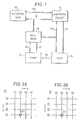
- an address pattern/data generator 10 also generates a test data pattern.
- an address pattern specified by an address bus 15a which is generated by the address pattern/data generator 10 is applied to an address changeover means (address/data selector 11), and on the other hand, data specified by a data bus 16 is supplied to both the address/data selector 11 and a fail memory device 12.
- the above data specified by the data bus 16 is also supplied to a semiconductor memory device 14 which is to be tested, through the address /data selector 11 by a data bus 17.
- An address specified by an address bus 15b is supplied to the fail memory device 12, from the address/data selector 11.
- the address pattern specified by the address bus 15a which is applied to the address/data selector 11, and the address specified by the address bus 15b which is supplied from the address/data selector 11, are the same address. Accordingly, the same address is supplied to both the fail memory device 12 and the memory device 14.
- the content of the bit F1 is supplied to the comparator 13 as the signal 20 (indicating that the bit is defective), and prohibits the comparison to be performed for the bit M1.
- the address pattern specified by the address bus 15a and the address specified by the address bus 15b are not equal. That is, the X and Y addresses of the address specified by the address bus 15b comprise the interchanged X and Y addresses of the address pattern specified by the address bus 15a.
- this interchanged address namely, the address specified by the address bus 15b is supplied to both the fail memory device 12 and the memory device 14, as in the normal mode.
- difference from the normal mode lies in the fact that the address supplied to both the fail memory device 12 and the memory device 14, is the address which is interchanged at the address/data selector 11. This can be shown by the diagrams of Figs. 3A and 3B. Fig.
- the rest of the operation is identical to that upon normal mode operation, and accordingly, when a defective bit exists, the defective bit can be correctly masked.
- Fig. 4 is a block diagram showing the essential parts of the address system of Fig. 1, in which the comparator 13 is not shown, to simplify the diagram.
- Each of address selectors 22 and 26 comprises a pin selector 27, drive card 23, an address multiplexer 24, and the like.
- P1 through P6 designate drive pins.
- AO through All designate address bits. However, the contents of the address bits designated by the same symbol in the different stages are not necessarily the same.
- An address pattern generator is designated by the numeral 28.
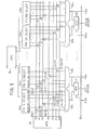
- Fig. 5 The essential part of the above address selectors 22 and 26, is the pin selector 27, and a more detailed diagram showing the construction of the pin selector is illustrated in Fig. 5.
- the example shown in Fig. 5 is a case in which twenty-one address bits, AO through A20, are used.
- the pin selector comprises pin selecting circuit pairs 31a and 31b through 40a and 40b, a matrix part having NAND-gates 41a-1 through 41a-20, 41b-1 through 41b-20, ---, and NAND-gates 41a through 50b which mix the output signal from the above matrix part.
- Multiplexers 51 through 60 which multiplex the output fail memory addresses FMA supplied by NAND-gate pairs 41a and 41b through 50a and 50b, correspond to the address multiplexer 24 of Fig. 4. Accordingly, the multiplexers 51 through 60 are controlled by a multiplexing signal Sm, and apply their output signal to driver pins 1 through 10 of the driver card 23.
- the address bit AO of the pin selecting circuit 31a is set at a high level, and the other address bits of that pin selecting circuit are set at low levels.
- the address bit A6 of the pin selecting circuit 31b is set at a high level, and the other address bits of that pin selecting circuit are set at low levels.
- the output levels of the NAND-gates excluding the NAND-gates 41a-1 and 4lb-6 are forcibly set low, and the output signals of the NAND-gates 41a-1 and 4lb-6 respectively become of reversed logic as those of the address bits A0 and A6 of the address pattern generator 28.
- the NAND-gates at the output stage again reverse the logic of the above output signals, and therefore, the output fail memory addresses FMA of-the NAND-gates 41a and 41b become of the same phase as those of the outputs in the address bits AD and A6 of the address pattern generator 28.
- the address bit A6 of the pin selecting circuit 31a is set at a high level, and the other address bits of that pin selecting circuit are all set at low levels.
- the relationship between the address bits A0 and A6 becomes that of a swap mode.
- the output fail memory address FMA is used for accessing to both the memory device which is to be tested and the fail memory device.
- the testing of a semi- conductor memory device is simplified according to the illustrated semiconductor memory device testing apparatus and method since, after the defective bits are written-in to the fail memory device, the masking operation is not affected by the address swapping performed in the memory device which is to be tested.
Landscapes
- For Increasing The Reliability Of Semiconductor Memories (AREA)
- Tests Of Electronic Circuits (AREA)
Applications Claiming Priority (2)
| Application Number | Priority Date | Filing Date | Title |
|---|---|---|---|
| JP18245579 | 1979-12-27 | ||
| JP182455/79U | 1979-12-27 |
Publications (3)
| Publication Number | Publication Date |
|---|---|
| EP0031706A2 true EP0031706A2 (fr) | 1981-07-08 |
| EP0031706A3 EP0031706A3 (en) | 1981-08-26 |
| EP0031706B1 EP0031706B1 (fr) | 1984-11-07 |
Family
ID=16118563
Family Applications (1)
| Application Number | Title | Priority Date | Filing Date |
|---|---|---|---|
| EP80304670A Expired EP0031706B1 (fr) | 1979-12-27 | 1980-12-22 | Dispositif et procédé pour tester des dispositifs de mémoire semiconducteurs |
Country Status (3)
| Country | Link |
|---|---|
| US (1) | US4384348A (fr) |
| EP (1) | EP0031706B1 (fr) |
| DE (1) | DE3069611D1 (fr) |
Cited By (5)
| Publication number | Priority date | Publication date | Assignee | Title |
|---|---|---|---|---|
| EP0197363A1 (fr) * | 1985-03-26 | 1986-10-15 | Siemens Aktiengesellschaft | Procédé d'exploitation d'une mémoire à semi-conducteur avec possibilité de test parallèle intégré et circuit d'évaluation pour la réalisation de ce procédé |
| DE3732830A1 (de) * | 1987-09-29 | 1989-04-06 | Siemens Ag | Schaltungsanordnung zur pruefung der funktionsfaehigkeit einer komplexen schaltung |
| WO1989009471A3 (fr) * | 1988-04-01 | 1989-11-16 | Digital Equipment Corp | Procede et appareil d'autotest de memoire |
| EP0447995A3 (en) * | 1990-03-19 | 1992-09-23 | Advantest Corporation | Analyzing device for saving semiconductor memory failures |
| KR102013643B1 (ko) * | 2018-04-13 | 2019-10-21 | 주식회사 엑시콘 | 고속 번인 테스트 장치 및 방법 |
Families Citing this family (12)
| Publication number | Priority date | Publication date | Assignee | Title |
|---|---|---|---|---|
| US4751636A (en) * | 1981-03-09 | 1988-06-14 | General Signal Corp. | Memory management method and apparatus for initializing and/or clearing R/W storage areas |
| US4608687A (en) * | 1983-09-13 | 1986-08-26 | International Business Machines Corporation | Bit steering apparatus and method for correcting errors in stored data, storing the address of the corrected data and using the address to maintain a correct data condition |
| JPS6238600A (ja) * | 1985-08-14 | 1987-02-19 | Fujitsu Ltd | 半導体記憶装置 |
| US5157664A (en) * | 1989-09-21 | 1992-10-20 | Texas Instruments Incorporated | Tester for semiconductor memory devices |
| US5210860A (en) * | 1990-07-20 | 1993-05-11 | Compaq Computer Corporation | Intelligent disk array controller |
| DE4028819A1 (de) * | 1990-09-11 | 1992-03-12 | Siemens Ag | Schaltungsanordnung zum testen eines halbleiterspeichers mittels paralleltests mit verschiedenen testbitmustern |
| JPH05281299A (ja) * | 1992-03-31 | 1993-10-29 | Ando Electric Co Ltd | アドレスパターン発生器 |
| US5357529A (en) * | 1992-04-24 | 1994-10-18 | Digital Equipment Corporation | Error detecting and correcting apparatus and method with transparent test mode |
| JP3267981B2 (ja) * | 1996-10-15 | 2002-03-25 | 株式会社アドバンテスト | メモリ試験装置及びこの試験装置をram試験モードとrom試験モードとに切り替える方法 |
| US6078637A (en) | 1998-06-29 | 2000-06-20 | Cypress Semiconductor Corp. | Address counter test mode for memory device |
| US7320100B2 (en) * | 2003-05-20 | 2008-01-15 | Cray Inc. | Apparatus and method for memory with bit swapping on the fly and testing |
| US7184916B2 (en) * | 2003-05-20 | 2007-02-27 | Cray Inc. | Apparatus and method for testing memory cards |
Family Cites Families (1)
| Publication number | Priority date | Publication date | Assignee | Title |
|---|---|---|---|---|
| US4183096A (en) * | 1978-05-25 | 1980-01-08 | Bell Telephone Laboratories, Incorporated | Self checking dynamic memory system |
-
1980
- 1980-12-22 DE DE8080304670T patent/DE3069611D1/de not_active Expired
- 1980-12-22 EP EP80304670A patent/EP0031706B1/fr not_active Expired
- 1980-12-29 US US06/221,329 patent/US4384348A/en not_active Expired - Lifetime
Cited By (5)
| Publication number | Priority date | Publication date | Assignee | Title |
|---|---|---|---|---|
| EP0197363A1 (fr) * | 1985-03-26 | 1986-10-15 | Siemens Aktiengesellschaft | Procédé d'exploitation d'une mémoire à semi-conducteur avec possibilité de test parallèle intégré et circuit d'évaluation pour la réalisation de ce procédé |
| DE3732830A1 (de) * | 1987-09-29 | 1989-04-06 | Siemens Ag | Schaltungsanordnung zur pruefung der funktionsfaehigkeit einer komplexen schaltung |
| WO1989009471A3 (fr) * | 1988-04-01 | 1989-11-16 | Digital Equipment Corp | Procede et appareil d'autotest de memoire |
| EP0447995A3 (en) * | 1990-03-19 | 1992-09-23 | Advantest Corporation | Analyzing device for saving semiconductor memory failures |
| KR102013643B1 (ko) * | 2018-04-13 | 2019-10-21 | 주식회사 엑시콘 | 고속 번인 테스트 장치 및 방법 |
Also Published As
| Publication number | Publication date |
|---|---|
| DE3069611D1 (en) | 1984-12-13 |
| EP0031706A3 (en) | 1981-08-26 |
| EP0031706B1 (fr) | 1984-11-07 |
| US4384348A (en) | 1983-05-17 |
Similar Documents
| Publication | Publication Date | Title |
|---|---|---|
| EP0031706B1 (fr) | Dispositif et procédé pour tester des dispositifs de mémoire semiconducteurs | |
| KR100197636B1 (ko) | 페일메모리 장치 | |
| US6185709B1 (en) | Device for indicating the fixability of a logic circuit | |
| KR100327136B1 (ko) | 반도체 메모리 장치 및 이 장치의 병렬 비트 테스트 방법 | |
| US6128756A (en) | System for optimizing the testing and repair time of a defective integrated circuit | |
| US5315552A (en) | Memory module, method for control thereof and method for setting fault bit table for use therewith | |
| US5475815A (en) | Built-in-self-test scheme for testing multiple memory elements | |
| US5299202A (en) | Method and apparatus for configuration and testing of large fault-tolerant memories | |
| US6353563B1 (en) | Built-in self-test arrangement for integrated circuit memory devices | |
| US5109360A (en) | Row/column address interchange for a fault-tolerant memory system | |
| GB2129585A (en) | Memory system including a faulty rom array | |
| EP0281740B1 (fr) | Mémoires et leur essai | |
| EP1647031B1 (fr) | Dispositif memoire et procede de stockage d'adresses defectueuses d'une cellule memoire | |
| KR19990045167A (ko) | 반도체 메모리 시험장치의 불량 해석 메모리 및그 기억방법 | |
| US5422892A (en) | Integrated circuit test arrangement and method for maximizing the use of tester comparator circuitry to economically test wide data I/O memory devices | |
| EP0090219B1 (fr) | Système de mémoire restructuré par algorithme de permutation déterministe | |
| US5386383A (en) | Method and apparatus for controlling dynamic random access memory devices | |
| EP0096780B1 (fr) | Méthode d'exclusion d'alignement d'erreur pour empêcher le réalignement de défauts de mémoire antérieurement appariés | |
| EP0096779B1 (fr) | Arrangement pour la dispersion d'erreur multibit afin de fournir une mémoire à semi-conducteur tolérant des défauts | |
| US6552937B2 (en) | Memory device having programmable column segmentation to increase flexibility in bit repair | |
| US7020033B2 (en) | Semiconductor memory apparatus and self-repair method | |
| KR20010040999A (ko) | 디지털 반도체 회로를 테스트하기 위한 회로 및 방법 | |
| US6055611A (en) | Method and apparatus for enabling redundant memory | |
| EP0366757B1 (fr) | Procede et appareil d'autotest de memoire | |
| US6092227A (en) | Test circuit |
Legal Events
| Date | Code | Title | Description |
|---|---|---|---|
| PUAI | Public reference made under article 153(3) epc to a published international application that has entered the european phase |
Free format text: ORIGINAL CODE: 0009012 |
|
| PUAL | Search report despatched |
Free format text: ORIGINAL CODE: 0009013 |
|
| AK | Designated contracting states |
Designated state(s): AT BE CH DE FR GB IT LU NL SE |
|
| AK | Designated contracting states |
Designated state(s): DE FR GB |
|
| RBV | Designated contracting states (corrected) |
Designated state(s): DE FR GB |
|
| 17P | Request for examination filed |
Effective date: 19810928 |
|
| GRAA | (expected) grant |
Free format text: ORIGINAL CODE: 0009210 |
|
| AK | Designated contracting states |
Designated state(s): DE FR GB |
|
| REF | Corresponds to: |
Ref document number: 3069611 Country of ref document: DE Date of ref document: 19841213 |
|
| ET | Fr: translation filed | ||
| PLBE | No opposition filed within time limit |
Free format text: ORIGINAL CODE: 0009261 |
|
| STAA | Information on the status of an ep patent application or granted ep patent |
Free format text: STATUS: NO OPPOSITION FILED WITHIN TIME LIMIT |
|
| 26N | No opposition filed | ||
| PGFP | Annual fee paid to national office [announced via postgrant information from national office to epo] |
Ref country code: FR Payment date: 19941209 Year of fee payment: 15 |
|
| PGFP | Annual fee paid to national office [announced via postgrant information from national office to epo] |
Ref country code: GB Payment date: 19941213 Year of fee payment: 15 |
|
| PGFP | Annual fee paid to national office [announced via postgrant information from national office to epo] |
Ref country code: DE Payment date: 19941222 Year of fee payment: 15 |
|
| PG25 | Lapsed in a contracting state [announced via postgrant information from national office to epo] |
Ref country code: GB Effective date: 19951222 |
|
| GBPC | Gb: european patent ceased through non-payment of renewal fee |
Effective date: 19951222 |
|
| PG25 | Lapsed in a contracting state [announced via postgrant information from national office to epo] |
Ref country code: FR Effective date: 19960830 |
|
| PG25 | Lapsed in a contracting state [announced via postgrant information from national office to epo] |
Ref country code: DE Effective date: 19960903 |
|
| REG | Reference to a national code |
Ref country code: FR Ref legal event code: ST |