EP0031987B1 - Source de tension de référence pour une source de tension continue stabilisée - Google Patents
Source de tension de référence pour une source de tension continue stabilisée Download PDFInfo
- Publication number
- EP0031987B1 EP0031987B1 EP80300052A EP80300052A EP0031987B1 EP 0031987 B1 EP0031987 B1 EP 0031987B1 EP 80300052 A EP80300052 A EP 80300052A EP 80300052 A EP80300052 A EP 80300052A EP 0031987 B1 EP0031987 B1 EP 0031987B1
- Authority
- EP
- European Patent Office
- Prior art keywords
- reference voltage
- variable resistor
- movable contact
- voltage
- output voltage
- Prior art date
- Legal status (The legal status is an assumption and is not a legal conclusion. Google has not performed a legal analysis and makes no representation as to the accuracy of the status listed.)
- Expired
Links
Images


Classifications
-
- G—PHYSICS
- G05—CONTROLLING; REGULATING
- G05F—SYSTEMS FOR REGULATING ELECTRIC OR MAGNETIC VARIABLES
- G05F1/00—Automatic systems in which deviations of an electric quantity from one or more predetermined values are detected at the output of the system and fed back to a device within the system to restore the detected quantity to its predetermined value or values, i.e. retroactive systems
- G05F1/10—Regulating voltage or current
- G05F1/46—Regulating voltage or current wherein the variable actually regulated by the final control device is DC
- G05F1/468—Regulating voltage or current wherein the variable actually regulated by the final control device is DC characterised by reference voltage circuitry, e.g. soft start, remote shutdown
Definitions
- This invention relates to a reference voltage generating circuit in DC regulated power source apparatus, and more particularly in DC regulated power source apparatus incorporated in an electronic device.
- Electronic devices such as communications equipment or sequence controllers and numerical control units of controlling machine tools, generally incorporate a DC regulated power source device which supplies their electronic components with a regulated DC voltage.
- DC regulated power sources include a reference power source for generating a reference voltage, as well as an output voltage control element.
- the output voltage control element constantly compares the output voltage against the reference voltage and functions to hold the output voltage constant at all times by restoring the output voltage to the reference voltage when the former attempts to rise, or by raising the output voltage up to the reference voltage when the former attempts to drop.
- the reference voltage is usually produced through use of a Zener diode.
- Zener voltages can differ slightly even for Zener diodes of the same type or grade, using the voltage obtained from such diodes as a reference voltage results in irregularities among the devices that receive the output voltage from the DC regulated apparatus. It is therefore conventional practice to employ a Zener diode of a higher Zener voltage than the reference voltage, and to divide this high Zener voltage down to an accurate reference voltage by means of a potentiometer.
- a reference voltage generating circuit in a DC regulated power supply, for supplying a regulated DC output voltage, including an error amplifier for detecting a difference between a reference voltage and an output voltage of the power supply, and a voltage control circuit responsive to a difference output signal from the error amplifier to control the output voltage in such a manner as to limit the difference between the reference voltage and output voltage to zero,
- the reference voltage generating circuit comprising a reference voltage source and a first variable resistor connected in parallel with the reference voltage source, characterised in that the reference voltage generating circuit further comprises a second variable resistor one end of which is connected to the negative side of said reference voltage source, a third variable resistor one end of which is connected to a voltage source side different from that to which the one end of the second variable resistor is connected, and switching means operable to connect a movable contact piece of said first variable resistor, movable to vary the resistance of the first variable resistor, to the other end of said second variable resistor or to the other end of said third variable resistor
- An embodiment of this invention can provide a reference voltage generating circuit in DC regulated power source apparatus for incorporation in a variety of electronic equipment, the output of which apparatus can be finely adjusted to correct for discrepancies in the reference voltage applied by a reference power source, and which allows the output voltage of the apparatus to be shifted to a preset value by an operation command signal which does not require the intervention of an operator, or by a simple switching procedure performed by an operator.
- An embodiment of the present invention can provide a reference voltage generating circuit in DC regulated power source apparatus such that the output voltage of the apparatus can be finely adjusted in a continuous manner.
- An embodiment of the present invention can provide a DC reference voltage generating circuit in DC regulated power source apparatus such that the output voltage of the apparatus, which has been adjusted to a prescribed value, can be shifted manually or automatically by a fixed amount.
- An embodiment of the present invention can provide a reference voltage generating circuit in DC regulated power source apparatus such that, when the output voltage of the apparatus is shifted to a fixed voltage that is higher than a prescribed value, any error in the output voltage is minimized even if a reference voltage fluctuates.
- FIG. 1 Illustrated in Fig. 1 is a functional block diagram of a typical DC regulated power source apparatus which has long been known in the art.
- the apparatus includes a rectifying and smoothing circuit 1, a voltage control circuit 2, a differential amplifier 3, and a reference voltage power source 4 which supplies a reference voltage E s .
- the differential amplifier 3 detects a difference in voltage between the reference voltage E s and an output voltage V o , and responds by controlling the voltage control circuit 2 in such a manner that the difference in voltage is limited to zero, thereby equalizing the output voltage V o and reference voltage E s at all times.
- a Zener diode is employed in the reference voltage power source 4.
- Zener diodes may be of an identical type or grade, it is common for such diodes to provide Zener voltages which differ from one another to an extremely small degree. A prescribed voltage therefore cannot be obtained with the apparatus of Fig. 1 as long as it is not possible to acquire Zener diodes which can provide Zener voltages which are identical to the reference voltage E s . It is for this reason that the systems shown in Figs. 2 and 3 are adopted in the prior art.
- a rheostat 5 is employed to divide the reference voltage E s , with the output voltage Vo being adjusted to a desired value within the range of the reference voltage E s .
- the output voltage Vo is adjusted to a prescribed voltage through multiplying the reference voltage E s by the ratio of the resistance value R of rheostat 5 to the divided resistance r.
- the present invention is based upon the DC regulated power source apparatus of the types shown in Figs. 1 through 3, in which a differential amplifier is used to compare an output voltage against a reference voltage, with a voltage control circuit being controlled in response to the output of the differential amplifier to hold the output voltage of the apparatus at a prescribed value.
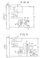
- Fig. 4 is a circuit diagram illustrating an embodiment of the present invention.
- the arrangement includes a rectifying and smoothing circuit 11, a voltage control circuit 12, a differential amplifier 13, a reference power source 14, a variable resistor 15, a total resistance R, a three-point type switch 16, and rheostats 17, 18 having respective resistance values of R, and R 2 .
- the arrangement of Fig. 4 operates as follows. Movable contact a of switch 16 ordinarily is switched to neutral pole N.
- the output voltage V o " is set to the reference value as in the prior art by adjusting the rheostat 15 to change the dividing ratio a.
- the reference voltage Eg of the reference voltage source 14 is preset to a value which is higher than the operating voltage of the electronic circuitry, such as a value which is twice the operating voltage.
- the above equation shows that the output voltage V o " drops to a fixed value by varying the dividing ratio a until it attains the value a L .
- the fixed value to which the output voltage V o " drops can be varied by changing the value of R 1 through adjustment of the rheostat 17. Restoring the output voltage V o " to the original value can be accomplished merely by switching the movable contact a back to the neutral position N.
- the above euation shows that the output voltage V o " rises to a fixed value by varying the dividing ratio until it attains the value a H .
- the fixed value to which the output voltage V o " rises can be varied by changing the value of R 2 through adjustment of the rheostat 18.
- the output voltage V o " can be. restored to the original value merely by switching the movable contact a back to the neutral position N.
- the movable contact a can be switched over manually or automatically through the use of suitable drive means.
- suitable drive means One example in which the latter can be accomplished is by means of an electromagnetic switch whose contact is adapted to be switched over by an electromagnetic force.
- a switching circuit is designated generally at 19, the circuit including stationary contacts h, n, I, a movable contact M, and a drive circuit 191 for actuating the movable contact M.
- Drive circuit 191 has a signal input terminal S. Movable contact M is switched to stationary contact n when signal input terminal S is at zero potential, to stationary contact h when input terminal S is at a positive potential (+5 volts), and to a stationary contact / when input terminal S is at a negative potential (-5 volts).
- Rheostat 17 is connected to stationary contact /, and semi-fixed variable resistor 18 to stationary contact h.
- An OR gate 20 has its output side connected to the signal input terminal S of drive circuit 191, and has one input terminal X connected to a driving signal generator and its other input terminal connected to the variable contact of three-point switch 21. Sources of +5 and -5 volt signals are shown at 23 and 22, respectively.
- a -5 volt signal from the driving signal generator is applied to the input terminal X of OR gate 20, whereupon the signal is delivered to drive circuit 191 through the OR gate.
- Drive circuit 191 responds by switching the movable contact M to the stationary contact /, whereby the output voltage is shifted downward by a fixed value as in the foregoing embodiment.
- a +5 volt signal from the driving signal generator is applied to the input terminal X of OR gate 20, whereupon the signal is delivered to drive circuit 191 through the OR gate.
- Drive circuit 191 now responds by switching the movable contact M to the stationary contact h, whereby the output voltage is shifted upward by a fixed value as in the foregoing embodiment. On the other hand, no signals are delivered to drive circuit 191 from the driving signal generator when the output voltage is to be maintained at the prescribed value. On such occasions the movable contact M is switched to the stationary contact n. If it is now desired to shift the output voltage upward or downward by a fixed value through a manual instead of the automatic method, the three-point switch 21 need only be manipulated by hand to apply the +5 volt signal or -5 volt signal to drive circuit 191.
- the range over which the output voltage can be shifted from the reference value is decided by the value of the reference voltage Eg supplied by the reference voltage power source 14, the resistance values r, and r 2 of the divided parts of the total resistance of the variable resistor 15, and the resistance values R, and R 2 of the rheostats 17 and 18.
- Fig. 6 is a simplified circuit diagram of the circuitry of the two foregoing embodiments.
- T is a terminal which schematically represents the movable contact a of switch 16 in Fig. 4 or movable contact M in Fig. 15.
- Terminal T can be interconnected to either of terminals H and L (which correspond to high and low voltage positions H and L in Fig. 4 and stationary contacts h and I in Fig. 5).
- the range ⁇ V o " over which the output voltage V o " can be shifted is defined by the following: where ⁇ V" oL represents downward shift when the output voltage is reduced by a fixed value to below its rated or prescribed value, and where ⁇ V" oL represents upward shift when the output voltage is increased by a fixed value to above its rated or prescribed value.
- E e is a separate power source of a higher voltage than E o , and is suitably regulated by a Zener diode or the like.
- H, T and L correspond to H, T and L in Fig. 6.
- the range ⁇ V" oH over which the output voltage is shifted when terminals H an T are interconnected is given by the following equation.
- the present invention provides first output voltage varying means (rheostat 15) for setting an output voltage to a prescribed value, thereby to allow a variance in reference voltage to be corrected.
- the invention further provides second output voltage varying means (rheostat 17 or 18) for temporarily shifting the prescribed output voltage, set by the first output voltage varying means, to a preset value, thereby allowing the output voltage to be shifted through a simple operation whenever maintenance and inspection are performed. This eliminates the troublesome adjustment procedure encountered in the prior art, wherein adjustment must be performed while a voltmeter is observed.
- actuating the output voltage varying means by an externally applied signal allows a test step, for confirming circuit operating margin, to be inserted into a series of automated test steps.
- two reference voltage sources may be used to provide a voltage difference which is divided down to a voltage that may then be employed as the reference voltage which is applied to a differential amplifier. The shifted voltage will therefore attain a value in conformance with the planned value.
Landscapes
- Engineering & Computer Science (AREA)
- Physics & Mathematics (AREA)
- Electromagnetism (AREA)
- General Physics & Mathematics (AREA)
- Radar, Positioning & Navigation (AREA)
- Automation & Control Theory (AREA)
- Continuous-Control Power Sources That Use Transistors (AREA)
Claims (5)


Priority Applications (2)
| Application Number | Priority Date | Filing Date | Title |
|---|---|---|---|
| EP80300052A EP0031987B1 (fr) | 1980-01-04 | 1980-01-04 | Source de tension de référence pour une source de tension continue stabilisée |
| DE8080300052T DE3071548D1 (en) | 1980-01-04 | 1980-01-04 | Reference voltage generating circuit in dc regulated power source apparatus |
Applications Claiming Priority (1)
| Application Number | Priority Date | Filing Date | Title |
|---|---|---|---|
| EP80300052A EP0031987B1 (fr) | 1980-01-04 | 1980-01-04 | Source de tension de référence pour une source de tension continue stabilisée |
Publications (2)
| Publication Number | Publication Date |
|---|---|
| EP0031987A1 EP0031987A1 (fr) | 1981-07-15 |
| EP0031987B1 true EP0031987B1 (fr) | 1986-04-16 |
Family
ID=8187068
Family Applications (1)
| Application Number | Title | Priority Date | Filing Date |
|---|---|---|---|
| EP80300052A Expired EP0031987B1 (fr) | 1980-01-04 | 1980-01-04 | Source de tension de référence pour une source de tension continue stabilisée |
Country Status (2)
| Country | Link |
|---|---|
| EP (1) | EP0031987B1 (fr) |
| DE (1) | DE3071548D1 (fr) |
Cited By (1)
| Publication number | Priority date | Publication date | Assignee | Title |
|---|---|---|---|---|
| DE4114073A1 (de) * | 1991-04-30 | 1992-11-05 | Bosch Gmbh Robert | Schaltungsanordnung zur stabilisierung einer spannung |
Families Citing this family (3)
| Publication number | Priority date | Publication date | Assignee | Title |
|---|---|---|---|---|
| EP0103455A3 (fr) * | 1982-09-10 | 1984-07-11 | Fujitsu Limited | Circuit pour source de puissance |
| FR2654232A1 (fr) * | 1989-11-07 | 1991-05-10 | Europ Rech Electr Lab | Generateur de tensions continues pour l'alimentation d'une carte a circuit integre. |
| US5177431A (en) * | 1991-09-25 | 1993-01-05 | Astec International Ltd. | Linear programming circuit for adjustable output voltage power converters |
Family Cites Families (2)
| Publication number | Priority date | Publication date | Assignee | Title |
|---|---|---|---|---|
| US3566252A (en) * | 1968-10-01 | 1971-02-23 | Forbro Design Corp | Method of and means for digital programming of regulated power supplies |
| US3577064A (en) * | 1969-03-12 | 1971-05-04 | Forbro Design Corp | Automatic error detection and indication in a remotely programmable regulated power supply |
-
1980
- 1980-01-04 DE DE8080300052T patent/DE3071548D1/de not_active Expired
- 1980-01-04 EP EP80300052A patent/EP0031987B1/fr not_active Expired
Non-Patent Citations (1)
| Title |
|---|
| ELEKTOR, vol. 2, no. 7/8, July/August 1976, pages 739-740 Canterbury, G.B. G. EBNER: "O-30 V/1 A, stabilised" * |
Cited By (2)
| Publication number | Priority date | Publication date | Assignee | Title |
|---|---|---|---|---|
| DE4114073A1 (de) * | 1991-04-30 | 1992-11-05 | Bosch Gmbh Robert | Schaltungsanordnung zur stabilisierung einer spannung |
| DE4114073C3 (de) * | 1991-04-30 | 2001-07-05 | Bosch Gmbh Robert | Schaltungsanordnung zur Stabilisierung einer Spannung |
Also Published As
| Publication number | Publication date |
|---|---|
| DE3071548D1 (en) | 1986-05-22 |
| EP0031987A1 (fr) | 1981-07-15 |
Similar Documents
| Publication | Publication Date | Title |
|---|---|---|
| US4321525A (en) | Reference voltage generating circuit in a DC power supply | |
| US4618779A (en) | System for parallel power supplies | |
| DE69018600T2 (de) | Stromverteilungssteuerung für Wechselrichter im Parallelbetrieb. | |
| US5521809A (en) | Current share circuit for DC to DC converters | |
| DE69620929T2 (de) | Batterieladegerät | |
| DE2056208B2 (de) | Regelvorrichtung fuer eine aus mindestens zwei getrennten einheiten bestehende heiz- und/oder kuehlanlage | |
| EP0520439A2 (fr) | Générateur électronique de courant de soudage pour le soudage à arc pulsé | |
| DE69622921T2 (de) | Steuerungssystem für ein lineares Elektromagnetventil | |
| DE3110350A1 (de) | Lichtbogenschweissvorrichtung | |
| EP0031987A1 (fr) | Source de tension de référence pour une source de tension continue stabilisée | |
| EP0543037B1 (fr) | Circuit de sortie intégré et paramétrable dans un circuit intégré | |
| EP0354269A1 (fr) | Circuit pour le contrôle de la résistance de contact d'un potentiomètre | |
| US4629966A (en) | Dual current limiting voltage regulator | |
| SU1205787A3 (ru) | Стабилизированный источник питани посто нного тока с узлом контрол выходного напр жени | |
| US3934239A (en) | Adjustable electronic load-alarm relay | |
| US4396986A (en) | Digital DC power supply with current and voltage measurement | |
| KR830001312B1 (ko) | 직류 안정화 전원장치 | |
| KR0139078B1 (ko) | 마이크로컴퓨터 제어식 저항사고 위치진단기회로 | |
| US4323838A (en) | RMS Controlled load tap changing transformer | |
| EP0725995B1 (fr) | Installation d'alimentation a distance | |
| CN114280524B (zh) | 基于模糊控制的集成电路测试系统校准方法及装置 | |
| DE3439115C2 (fr) | ||
| EP0112380B1 (fr) | Circuit convertisseur de frequence en courant | |
| US20030080759A1 (en) | Method and apparatus for optimizing the accuracy of an electronic circuit | |
| US3392324A (en) | Constant current circuit for determination of printed circuit acceptability |
Legal Events
| Date | Code | Title | Description |
|---|---|---|---|
| PUAI | Public reference made under article 153(3) epc to a published international application that has entered the european phase |
Free format text: ORIGINAL CODE: 0009012 |
|
| AK | Designated contracting states |
Designated state(s): DE FR GB |
|
| 17P | Request for examination filed |
Effective date: 19820106 |
|
| RAP1 | Party data changed (applicant data changed or rights of an application transferred) |
Owner name: FANUC LIMITED |
|
| RAP1 | Party data changed (applicant data changed or rights of an application transferred) |
Owner name: FANUC LTD |
|
| GRAA | (expected) grant |
Free format text: ORIGINAL CODE: 0009210 |
|
| AK | Designated contracting states |
Kind code of ref document: B1 Designated state(s): DE FR GB |
|
| REF | Corresponds to: |
Ref document number: 3071548 Country of ref document: DE Date of ref document: 19860522 |
|
| ET | Fr: translation filed | ||
| PLBE | No opposition filed within time limit |
Free format text: ORIGINAL CODE: 0009261 |
|
| STAA | Information on the status of an ep patent application or granted ep patent |
Free format text: STATUS: NO OPPOSITION FILED WITHIN TIME LIMIT |
|
| 26N | No opposition filed | ||
| PGFP | Annual fee paid to national office [announced via postgrant information from national office to epo] |
Ref country code: GB Payment date: 19901227 Year of fee payment: 12 |
|
| PGFP | Annual fee paid to national office [announced via postgrant information from national office to epo] |
Ref country code: FR Payment date: 19901228 Year of fee payment: 12 |
|
| PG25 | Lapsed in a contracting state [announced via postgrant information from national office to epo] |
Ref country code: GB Effective date: 19920104 |
|
| GBPC | Gb: european patent ceased through non-payment of renewal fee | ||
| PG25 | Lapsed in a contracting state [announced via postgrant information from national office to epo] |
Ref country code: FR Effective date: 19920930 |
|
| REG | Reference to a national code |
Ref country code: FR Ref legal event code: ST |
|
| PGFP | Annual fee paid to national office [announced via postgrant information from national office to epo] |
Ref country code: DE Payment date: 19960115 Year of fee payment: 17 |
|
| PG25 | Lapsed in a contracting state [announced via postgrant information from national office to epo] |
Ref country code: DE Effective date: 19971001 |