EP0033172A1 - Schaltung zur Korrektur der Phasendifferenzen zwischen Abtast-Steuersignalen und Synchronisationssignalen in einem Fernsehempfänger - Google Patents
Schaltung zur Korrektur der Phasendifferenzen zwischen Abtast-Steuersignalen und Synchronisationssignalen in einem Fernsehempfänger Download PDFInfo
- Publication number
- EP0033172A1 EP0033172A1 EP81200039A EP81200039A EP0033172A1 EP 0033172 A1 EP0033172 A1 EP 0033172A1 EP 81200039 A EP81200039 A EP 81200039A EP 81200039 A EP81200039 A EP 81200039A EP 0033172 A1 EP0033172 A1 EP 0033172A1
- Authority
- EP
- European Patent Office
- Prior art keywords
- output
- signals
- signal
- value
- synchronization
- Prior art date
- Legal status (The legal status is an assumption and is not a legal conclusion. Google has not performed a legal analysis and makes no representation as to the accuracy of the status listed.)
- Granted
Links
- 230000000087 stabilizing effect Effects 0.000 claims abstract 2
- 230000000737 periodic effect Effects 0.000 claims description 5
- 230000010354 integration Effects 0.000 claims description 4
- 238000012423 maintenance Methods 0.000 claims 2
- 230000008030 elimination Effects 0.000 claims 1
- 238000003379 elimination reaction Methods 0.000 claims 1
- 230000001360 synchronised effect Effects 0.000 abstract description 5
- 238000001914 filtration Methods 0.000 description 14
- 239000008186 active pharmaceutical agent Substances 0.000 description 8
- 239000003990 capacitor Substances 0.000 description 6
- 230000000630 rising effect Effects 0.000 description 6
- 235000021183 entrée Nutrition 0.000 description 5
- 238000004364 calculation method Methods 0.000 description 4
- 230000000295 complement effect Effects 0.000 description 3
- 238000013139 quantization Methods 0.000 description 3
- 238000000926 separation method Methods 0.000 description 3
- 230000006641 stabilisation Effects 0.000 description 3
- 238000006073 displacement reaction Methods 0.000 description 2
- 238000004519 manufacturing process Methods 0.000 description 2
- 238000011105 stabilization Methods 0.000 description 2
- PCTMTFRHKVHKIS-BMFZQQSSSA-N (1s,3r,4e,6e,8e,10e,12e,14e,16e,18s,19r,20r,21s,25r,27r,30r,31r,33s,35r,37s,38r)-3-[(2r,3s,4s,5s,6r)-4-amino-3,5-dihydroxy-6-methyloxan-2-yl]oxy-19,25,27,30,31,33,35,37-octahydroxy-18,20,21-trimethyl-23-oxo-22,39-dioxabicyclo[33.3.1]nonatriaconta-4,6,8,10 Chemical compound C1C=C2C[C@@H](OS(O)(=O)=O)CC[C@]2(C)[C@@H]2[C@@H]1[C@@H]1CC[C@H]([C@H](C)CCCC(C)C)[C@@]1(C)CC2.O[C@H]1[C@@H](N)[C@H](O)[C@@H](C)O[C@H]1O[C@H]1/C=C/C=C/C=C/C=C/C=C/C=C/C=C/[C@H](C)[C@@H](O)[C@@H](C)[C@H](C)OC(=O)C[C@H](O)C[C@H](O)CC[C@@H](O)[C@H](O)C[C@H](O)C[C@](O)(C[C@H](O)[C@H]2C(O)=O)O[C@H]2C1 PCTMTFRHKVHKIS-BMFZQQSSSA-N 0.000 description 1
- 241000861223 Issus Species 0.000 description 1
- 240000008042 Zea mays Species 0.000 description 1
- 230000003416 augmentation Effects 0.000 description 1
- 238000013016 damping Methods 0.000 description 1
- 230000007547 defect Effects 0.000 description 1
- 238000010586 diagram Methods 0.000 description 1
- 230000000694 effects Effects 0.000 description 1
- 230000002349 favourable effect Effects 0.000 description 1
- 238000009432 framing Methods 0.000 description 1
- 230000036039 immunity Effects 0.000 description 1
- 244000045947 parasite Species 0.000 description 1
- 230000003071 parasitic effect Effects 0.000 description 1
- 238000011002 quantification Methods 0.000 description 1
- 230000000717 retained effect Effects 0.000 description 1
- 230000035945 sensitivity Effects 0.000 description 1
- 230000003068 static effect Effects 0.000 description 1
- 230000001052 transient effect Effects 0.000 description 1
Images



Classifications
-
- H—ELECTRICITY
- H04—ELECTRIC COMMUNICATION TECHNIQUE
- H04N—PICTORIAL COMMUNICATION, e.g. TELEVISION
- H04N5/00—Details of television systems
- H04N5/04—Synchronising
- H04N5/12—Devices in which the synchronising signals are only operative if a phase difference occurs between synchronising and synchronised scanning devices, e.g. flywheel synchronising
- H04N5/126—Devices in which the synchronising signals are only operative if a phase difference occurs between synchronising and synchronised scanning devices, e.g. flywheel synchronising whereby the synchronisation signal indirectly commands a frequency generator
Definitions
- the present invention relates to a circuit for correcting phase differences between the scanning control signals and the line synchronization signals in a television receiver.
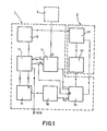
- the circuit according to the invention (FIG. 1) comprises two fundamental digital stages, namely a phase comparison stage 1 and a synchronization control stage 2.
- the counter 11 of the frequency divider is connected to the output of the reference oscillator 10 and has 12 output bits.
- the decoder 13 receives on the one hand the digital signal (at 12 bits) output from the counter 11, on the other hand the digital signal N + dN (at 12 bits) at the output of the adder 12, and, at the using 12 OR-exclusive circuits, connecting two to two the corresponding bits of the counter and the adder, and of a decoding circuit, delivers an output pulse S (of width 25 nanoseconds) if and only if all the corresponding bits coincide.
- This phase comparator comprises a logic circuit 14 and a counter 15; the logic circuit 14 receives on its first input the pulse S, of width 25 nanoseconds, delivered by the decoder 13 of the frequency divider and, on a second input, the line synchronization pulse V coming from the separation stage 3 , pulse whose width is close to 5 microseconds.
- the pulse S is sent to a first input of a flip-flop 21 and the pulse V to a first input of a flip-flop 22; a mid-line pulse M is produced approximately 32 microseconds after the pulse S and is sent to the second inputs of these flip-flops.
- B 1 and B 1 the two possible output signals of flip-flop 21 and B 2 and B 2 the two possible output signals of flip-flop 22
- the two output connections of B l and 8 2 are connected to the two inputs of an AND gate 23, while the two output connections of B 2 and B 1 are connected to the two inputs of another AND gate 24.
- the output connection of the AND gate 23 and that of the AND gate 24 are respectively connected to the two inputs of a door 25, the output connection of which delivers a pulse having for duration the phase difference between the pulse S and the pulse V.
- the output signal from the OR gate 25 is given by the expression:
- the phase difference TC is given by B 1 .8 2 , since, as shown in FIG. 3, B1.B 2 is zero.
- the pulse S arrives after the pulse V, it is B1.
- B 2 which is zero
- B 1 ⁇ B 2 which provides the phase difference between the two pulses.
- a third flip-flop 26, the two inputs of which receive the output signals from AND gates 23 and 24 respectively, provides the sign of this phase difference, according to that of the two output connections of this flip-flop on which a non-zero signal is present.
- Logic circuit 14 is associated with counter 15; this counter, here at 6 bits, receives on the one hand the signal TC expressing the phase difference between the pulses S and V, on the other hand a continuous sequence SC of periodic pulses of frequency 40 megahertz generated by the oscillator reference 10, and also, at each mid-line, the reset signal M, delivered by the decoder 13.
- this decoder 13 a fixed decoding takes place approximately every 32 microseconds after each reset of the counter 11 by the pulse S leaving the decoder (this is the correction time of the digital filtering circuit defined below, shorter than that corresponding to a half-line, which in fact makes it possible to fix the instant from which can be carried out resetting the counter 15).
- the counter 15 delivers a digital output signal at 6 bits representing the number of pulses of period 25 nanoseconds which follow one another during the counting time that constitutes the phase difference TC delivered by the logic circuit 14.
- the flip-flop 26 of this circuit 14 provides information on the sign of the phase difference (S after V, or V-after S), there is in fact a 7-bit signal (6 bits + 1 sign bit). If the output signal from flip-flop 26 is a "0”, the absolute value of the signal from counter 15 is transmitted directly; if it is a "1", it is the complement to two of this absolute value which is intended to be sent to stage 2 of synchronization control which will now be described in detail.
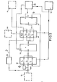
- This stage 2 which therefore receives the 7-bit digital signal defined above and delivered by the phase comparison stage 1, comprises on the one hand a state detector 30 and on the other hand a signal generator correction which is here a digital filtering circuit 31 (an embodiment of the detector 30 and of the circuit 31 is shown in FIGS. 4 and 5 respectively).
- a signal generator correction which is here a digital filtering circuit 31 (an embodiment of the detector 30 and of the circuit 31 is shown in FIGS. 4 and 5 respectively).
- This state detector 30 first comprises an AND-NO gate 40 (or NAND gate) receiving on its inputs the 6 bits which constitute the value of the digital output signal of the counter 15. If there is desynchronization, it that is to say, if the maximum capacity of the counter 15 is reached, these 6 bits have the value "1" and the NAND gate 40 then delivers, and only in this case, a "0".
- This output connection of the NAND gate 40 is returned to an input of an AND gate 41, the other input of which receives the output connection TC of the logic circuit 14 and the output of which is returned to the input of the counter 15; this gate 41 allows this saturation state of the counter 15 to be maintained for recording.
- the output of the NAND gate 40 is also sent to a shift register 42 with serial input and parallel outputs which records the situation observed at the output of the NAND gate 40 (and therefore of the counter 15) for eight consecutive lines; the choice of eight lines is only an example, we can adopt a higher number if we want to have better immunity against parasites.
- the 8 output bits of this register 42 are sent on the one hand to the eight inputs of a NOR gate 43 (or NOR gate) and on the other hand to the eight inputs of an AND gate 44, which can just as easily be replaced by a NAND gate and an inverter, and the outputs of these gates 43 and 44 constitute the two inputs of a rocker 45.
- a division of the difference x (n) by two is carried out prior to any filtering action, in order to reduce this difference x (n) to a value compatible with the capacity of the counter 15.
- the filter circuit is then switched to the synchronized position, with this circuit being preset at the time of switching to a value substantially equal to that taken by the signal dN after eight consecutive lines in the synchronization state (to free themselves from transient phenomena due to rebounds observed with analog filters).
- the filtering circuit 31 the structure and operation of which will now be described in more detail, can now again exercise the low-pass filter function which has just been specified above.
- the embodiment adopted here for the filtering circuit 31 comprises a switcher 32, an adder 33, a switcher 34, an accumulator 35, a register 36, a clock circuit 38, and the shift register 50 Also shown, in dashed lines, the adder 12, the counter 15 and the state detector 30 already described.
- the state detector 30 exclusively authorizes the execution of the three phases (a), (b), (c) for three time intervals T 1 , T2, T 3 or on the contrary exclusively the execution of divisions by two successive (for the return y (n) within the limit of the capacity of the counter 15) during the time interval T DS (the connections shown in FIG. 5 and accompanied by T 1 , T 21 T 3 or T DS are established exclusively during said intervals time, all other permanently existing links).
- the links T 1 , T 2 , T 3 are no longer established in the switch 32, but only the link T DS from the output DS of the flip-flop 45 of the state detector 30, to carry out from x (n) the divisions by two (in the shift register 50) which will make it possible to bring the output of the circuit 31 within the limit of the capacity of the counter 15 and to resynchronize the receiver.
- the output signal dN of the filtering circuit 31 is received by the adder 12, which also receives a signal N displayed in binary on appropriate inputs and equal to the ratio of the frequency of the reference oscillator 10 and the line frequency of the receiver (in this case, N is 40 megahertz / 15,625 megahertz, or 2,560).
- the signal finally obtained consists of pulses of variable period and equal to T x (N ⁇ dN), T being the period of the clock constituted by the reference oscillator 10, and these pulses constitute the useful line scan control signals delivered by the circuit according to the invention and available on the SCB output connection (see FIG. 1) of the decoder 13.
- the duty cycle of these signals depends on the control stage of scanning to which they are supplied (and which is not part of the invention): if the element controlled in this stage is a transistor, the duty cycle can be close to 50 ° so that these signals have a sufficient duration, whereas it could be significantly lower in the case where the element ordered is a thyristor.
- the value to be quantified numerically is not necessarily an exact multiple of the quantization step defined by the frequency of the oscillator 10. This value is then expressed in an approximate manner, either by default or by excess, and there is an incessant variation in the number of quantization steps between these two approximate values (immediately lower and greater than the real value to be quantified), leading to instability in the triggering line scanning and therefore a loss of alignment with the video signal, visible especially on vertical lines.
- This instability can be completely eliminated using the stabilization stage described with reference to FIGS. 7 and 8 and which is placed between the output of the decoder 13 and the SCB connection.
- a slot is generated in a known manner at the output SD of the decoder 13 representing a certain number of clock strokes (the output pulses of the oscillator 10) and therefore of constant width (see FIG. 8a), but whose flanks are affected by the instability due to the random framing by default or by excess of the real value to be quantified; it follows that, unlike the width of the slot, the remaining part of the period is not fixed but animated by this same instability (or "jitter", in English).
- These slots signals are sent from the decoder 13 to an integrator 60, which delivers the signal shown in FIG.
- the output signals from the NAND gate 63 constitute the useful signals, this time strictly stable, for line scanning control, available on the SCB connection of Figures 1 and 7. As shown in Figure 8f compared to Figure 8b, it suffices to move the tilt thresholds on the falling edges ( Figure 8b) by means of the voltages on the other input of comparators 61 and 62, to vary the width (FIG. 8f) of the useful line scanning control signals and therefore their duty cycle.
- a capacitor 65 makes it possible to give the sawtooth output signal of the integrator 60 a zero mean value. In an alternative embodiment, it may be advantageous, on the contrary, to be able to continuously adjust this average value. This possibility provides the following advantage: if the tilting thresholds remain fixed and if the average value of the sawtooth signal varies, there is a displacement of the position in phase of the scanning control signals available on the connection SCB.
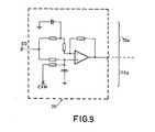
- FIG. 9 shows an exemplary embodiment of a circuit allowing such position adjustment in phase (this variant then replacing the assembly formed, in FIG. 7, by the integrator 60 and the capacitor 65).
- This circuit is a double integrator 70 of the output signal from the decoder 13, the upper part 70a of which ensures, as before, the generation of the sawtooth signal (weak integration) and the lower part of which 70b ensures the generation of a continuous signal ( strong integration) superimposed on the sawtooth signal at the output of this integrator 70.
- the displacement of the level of the continuous signal is controlled by a signal delivered on the CVM connection and of equal duration, for example, at the distance A ( r between the line return pulse from the final stage of lines (not shown) and a fixed phase mark relative to the oscillator (reset pulse for example).
- scan control outputs delivered on the SCB connection therefore varies depending on the value of this difference.
- the variant shown in FIG. 9 has fewer outputs than the equivalent part (integrator 60 + capacitor 6 5) of the stage shown in FIG. 7, which is very favorable for an integrated circuit embodiment.
- the sawtooth signal of FIG. 8b a shape such that the rising edge AB is significantly longer and the falling edge significantly shorter. With the falling edges becoming stiffer, any linearity defect at the tilt thresholds results in the signal of FIG. 8f by a weaker parasitic phase variation.
- this single threshold corresponding to the rising edge of the signal in FIG. 8f if this is what rising edge which acts on the controlled element (transistor or thyristor) of the scanning control stage, or corresponding on the contrary to the falling edge in the opposite case.
- the flank position which does not correspond to the single threshold can be determined by counting (and taking into account the considerations made above about the cyclical report).
- the use of a single threshold here offers the advantage of greater latitude for positioning on the falling edge, between the end B of a sawtooth and the bottom D of the next sawtooth.
Landscapes
- Engineering & Computer Science (AREA)
- Multimedia (AREA)
- Signal Processing (AREA)
- Stabilization Of Oscillater, Synchronisation, Frequency Synthesizers (AREA)
- Synchronizing For Television (AREA)
- Details Of Television Scanning (AREA)
Priority Applications (1)
| Application Number | Priority Date | Filing Date | Title |
|---|---|---|---|
| AT81200039T ATE13000T1 (de) | 1980-01-25 | 1981-01-14 | Schaltung zur korrektur der phasendifferenzen zwischen abtast-steuersignalen und synchronisationssignalen in einem fernsehempfaenger. |
Applications Claiming Priority (2)
| Application Number | Priority Date | Filing Date | Title |
|---|---|---|---|
| FR8001643A FR2474794A1 (fr) | 1980-01-25 | 1980-01-25 | Circuit de correction des ecarts de phase entre les signaux de commande de balayage et les signaux de synchronisation lignes dans un recepteur de television |
| FR8001643 | 1980-01-25 |
Publications (2)
| Publication Number | Publication Date |
|---|---|
| EP0033172A1 true EP0033172A1 (de) | 1981-08-05 |
| EP0033172B1 EP0033172B1 (de) | 1985-04-24 |
Family
ID=9237884
Family Applications (1)
| Application Number | Title | Priority Date | Filing Date |
|---|---|---|---|
| EP81200039A Expired EP0033172B1 (de) | 1980-01-25 | 1981-01-14 | Schaltung zur Korrektur der Phasendifferenzen zwischen Abtast-Steuersignalen und Synchronisationssignalen in einem Fernsehempfänger |
Country Status (8)
| Country | Link |
|---|---|
| US (1) | US4351002A (de) |
| EP (1) | EP0033172B1 (de) |
| JP (1) | JPS56112183A (de) |
| AT (1) | ATE13000T1 (de) |
| AU (1) | AU537972B2 (de) |
| CA (1) | CA1152634A (de) |
| DE (1) | DE3170082D1 (de) |
| FR (1) | FR2474794A1 (de) |
Cited By (2)
| Publication number | Priority date | Publication date | Assignee | Title |
|---|---|---|---|---|
| EP0174049A3 (de) * | 1984-09-03 | 1988-05-18 | Philips Patentverwaltung GmbH | Schaltungsanordnung zum Synchronisieren eines Signals |
| EP0290971A1 (de) * | 1987-05-13 | 1988-11-17 | Deutsche Thomson-Brandt GmbH | Schaltungsanordnung zur automatischen Umschaltung der Regelgeschwindigkeit eines Phasenregelkreises |
Families Citing this family (17)
| Publication number | Priority date | Publication date | Assignee | Title |
|---|---|---|---|---|
| NL8103437A (nl) * | 1981-07-21 | 1983-02-16 | Philips Nv | Synchroniseerschakeling voor een televisie-ontvanger. |
| JPS6063450A (ja) * | 1984-04-25 | 1985-04-11 | Hitachi Ltd | 欠陥検査装置 |
| JPH01158342U (de) * | 1988-04-22 | 1989-11-01 | ||
| JPH01171746U (de) * | 1988-05-13 | 1989-12-05 | ||
| JPH01173038U (de) * | 1988-05-30 | 1989-12-07 | ||
| JPH01173037U (de) * | 1988-05-30 | 1989-12-07 | ||
| JPH0274433A (ja) * | 1988-09-09 | 1990-03-14 | Daito Press Kogyo Kk | 自動車用後視鏡の支持アーム取り付け装置 |
| JPH02136347A (ja) * | 1988-11-16 | 1990-05-24 | Daito Press Kogyo Kk | 自動車用後視鏡の支持アーム操作装置 |
| JPH02136348A (ja) * | 1988-11-17 | 1990-05-24 | Daito Press Kogyo Kk | 自動車用後視鏡の支持アーム操作装置 |
| JPH0286840U (de) * | 1988-12-24 | 1990-07-10 | ||
| JPH0469245U (de) * | 1990-10-24 | 1992-06-18 | ||
| DE4214338A1 (de) * | 1992-05-04 | 1993-11-11 | Thomson Brandt Gmbh | Vertikalablenkschaltung für einen Fernsehempfänger |
| FR2710797B1 (fr) * | 1993-09-30 | 1995-12-15 | Sgs Thomson Microelectronics | Comparateur de phase numérique. |
| GB9623629D0 (en) * | 1996-11-13 | 1997-01-08 | Rca Thomson Licensing Corp | Width and phase control of blanking pulse |
| DE10049333C2 (de) * | 2000-10-05 | 2002-12-05 | Infineon Technologies Ag | Digitaler Phasenregelkreis |
| CN104966480B (zh) * | 2015-07-21 | 2017-08-25 | 京东方科技集团股份有限公司 | 阵列基板行驱动电路单元、驱动电路和显示面板 |
| CN120935312B (zh) * | 2025-10-13 | 2026-01-30 | 国科大杭州高等研究院 | 星载高分辨率成像系统的自校正时间同步装置和方法 |
Citations (2)
| Publication number | Priority date | Publication date | Assignee | Title |
|---|---|---|---|---|
| US4025951A (en) * | 1976-06-09 | 1977-05-24 | Gte Sylvania Incorporated | Vertical synchronizing circuit having adjustable sync pulse window |
| DE2726037A1 (de) * | 1976-06-09 | 1977-12-22 | Gte Sylvania Inc | Vertikalsynchronisierschaltung |
Family Cites Families (1)
| Publication number | Priority date | Publication date | Assignee | Title |
|---|---|---|---|---|
| US3821470A (en) * | 1973-05-21 | 1974-06-28 | Zenith Radio Corp | Phase correction for horizontal oscillator in cmos form |
-
1980
- 1980-01-25 FR FR8001643A patent/FR2474794A1/fr active Granted
-
1981
- 1981-01-14 AT AT81200039T patent/ATE13000T1/de not_active IP Right Cessation
- 1981-01-14 DE DE8181200039T patent/DE3170082D1/de not_active Expired
- 1981-01-14 EP EP81200039A patent/EP0033172B1/de not_active Expired
- 1981-01-15 CA CA000368597A patent/CA1152634A/en not_active Expired
- 1981-01-21 US US06/227,040 patent/US4351002A/en not_active Expired - Fee Related
- 1981-01-22 JP JP732881A patent/JPS56112183A/ja active Granted
- 1981-01-23 AU AU66570/81A patent/AU537972B2/en not_active Ceased
Patent Citations (2)
| Publication number | Priority date | Publication date | Assignee | Title |
|---|---|---|---|---|
| US4025951A (en) * | 1976-06-09 | 1977-05-24 | Gte Sylvania Incorporated | Vertical synchronizing circuit having adjustable sync pulse window |
| DE2726037A1 (de) * | 1976-06-09 | 1977-12-22 | Gte Sylvania Inc | Vertikalsynchronisierschaltung |
Non-Patent Citations (1)
| Title |
|---|
| IEEE TRANSACTIONS ON BROADCAST AND TELEVISION RECEIVERS, Vol. BT-19, No. 3, août 1973, pages 181-186, New York, U.S.A., H. YAMADA et al.: "A high stable television synchronizing system with a ceramic resonator" * |
Cited By (2)
| Publication number | Priority date | Publication date | Assignee | Title |
|---|---|---|---|---|
| EP0174049A3 (de) * | 1984-09-03 | 1988-05-18 | Philips Patentverwaltung GmbH | Schaltungsanordnung zum Synchronisieren eines Signals |
| EP0290971A1 (de) * | 1987-05-13 | 1988-11-17 | Deutsche Thomson-Brandt GmbH | Schaltungsanordnung zur automatischen Umschaltung der Regelgeschwindigkeit eines Phasenregelkreises |
Also Published As
| Publication number | Publication date |
|---|---|
| EP0033172B1 (de) | 1985-04-24 |
| CA1152634A (en) | 1983-08-23 |
| AU6657081A (en) | 1981-07-30 |
| FR2474794B1 (de) | 1985-02-01 |
| AU537972B2 (en) | 1984-07-19 |
| JPS634750B2 (de) | 1988-01-30 |
| DE3170082D1 (en) | 1985-05-30 |
| US4351002A (en) | 1982-09-21 |
| ATE13000T1 (de) | 1985-05-15 |
| JPS56112183A (en) | 1981-09-04 |
| FR2474794A1 (fr) | 1981-07-31 |
Similar Documents
| Publication | Publication Date | Title |
|---|---|---|
| EP0033172B1 (de) | Schaltung zur Korrektur der Phasendifferenzen zwischen Abtast-Steuersignalen und Synchronisationssignalen in einem Fernsehempfänger | |
| EP0159924B1 (de) | Digitaler "DIDON"-Demodulator | |
| FR2480544A1 (fr) | Circuit pour realiser une interpolation entre des valeurs prises dans deux rangees de donnees | |
| FR2594281A1 (fr) | Appareil d'estimation du bruit dans des signaux ayant des intervalles redondants | |
| EP0645888A1 (de) | Digitale Verzögerungsleitung | |
| FR2536620A1 (fr) | Televiseur numerique avec convertisseur analogique-numerique ayant un gain multiplexe dans le temps | |
| FR2482813A1 (fr) | Dispositif de codage et de signaux d'image et de son | |
| FR2476420A1 (fr) | Appareil de reproduction de signaux d'information | |
| FR2482814A1 (fr) | Procede et dispositif pour coder et decoder des signaux video par inversion repetitive de la polarite de ces signaux | |
| EP0342756B1 (de) | Fernsehsende- und Empfangssystem mit hoher Auflösung und verminderter Datenrate | |
| FR2526619A1 (fr) | Circuit de multiplication de la frequence de balayage | |
| EP0071506A1 (de) | Digitales Verfahren und digitale Einrichtung zur Berichtigung von Phasenfehlern eines abgetasteten Signals und seine Anwendung zur Berichtigung von Fernsehsignalen | |
| FR2543387A1 (de) | ||
| FR2515458A1 (fr) | Systeme detecteur de signaux fantomes avec reglage de la phase de la composante de synchronisation de sous-porteuse de chrominance | |
| FR2589302A1 (fr) | Systeme de thermographie infrarouge a sensibilite amelioree par accumulation progressive des lignes de l'image | |
| EP0023852A1 (de) | Verfahren und Vorrichtung zur Phasenregelung eines lokalen Taktgebers | |
| FR2490041A1 (fr) | Circuit pour engendrer un signal periodique variant en dent de scie | |
| FR2534102A1 (fr) | Reglage automatique de la grandeur de la salve de chrominance pour un televiseur numerique | |
| FR2614488A1 (fr) | Camera de television en couleur a plusieurs tubes possedant un systeme de reglage automatique de la coincidence | |
| CH625377A5 (de) | ||
| EP0365090B1 (de) | Einrichtung zum Verdoppeln der Rate von Fernsehbild-Signalen, und Fernsehbild-Dekodierer mit einer solchen Einrichtung | |
| FR2500245A1 (fr) | Systeme de traitement de signaux echantillonnes de television, systeme de transmission de signaux numeriques de television en couleur, procede de transcodage et recepteur de signaux numeriques de television | |
| EP0022405B1 (de) | Vorrichtung zum Codieren von Videofrequenz-Fernsehsignalen und diese Vorrichtung enthaltende Übertragungsausrüstung | |
| FR2502436A1 (fr) | Circuit pour la synchronisation de trame d'un dispositif de television | |
| EP0690623B1 (de) | Verfahren und Einrichtung zur Einfügung von asynchronen Daten in ein digitales Signal |
Legal Events
| Date | Code | Title | Description |
|---|---|---|---|
| PUAI | Public reference made under article 153(3) epc to a published international application that has entered the european phase |
Free format text: ORIGINAL CODE: 0009012 |
|
| AK | Designated contracting states |
Designated state(s): AT DE FR GB IT NL SE |
|
| 17P | Request for examination filed |
Effective date: 19811120 |
|
| RAP1 | Party data changed (applicant data changed or rights of an application transferred) |
Owner name: N.V. PHILIPS' GLOEILAMPENFABRIEKEN Owner name: LABORATOIRES D'ELECTRONIQUE ET DE PHYSIQUE APPLIQU |
|
| ITF | It: translation for a ep patent filed | ||
| GRAA | (expected) grant |
Free format text: ORIGINAL CODE: 0009210 |
|
| AK | Designated contracting states |
Designated state(s): AT DE FR GB IT NL SE |
|
| REF | Corresponds to: |
Ref document number: 13000 Country of ref document: AT Date of ref document: 19850515 Kind code of ref document: T |
|
| REF | Corresponds to: |
Ref document number: 3170082 Country of ref document: DE Date of ref document: 19850530 |
|
| PLBE | No opposition filed within time limit |
Free format text: ORIGINAL CODE: 0009261 |
|
| STAA | Information on the status of an ep patent application or granted ep patent |
Free format text: STATUS: NO OPPOSITION FILED WITHIN TIME LIMIT |
|
| 26N | No opposition filed | ||
| PGFP | Annual fee paid to national office [announced via postgrant information from national office to epo] |
Ref country code: FR Payment date: 19890120 Year of fee payment: 9 Ref country code: AT Payment date: 19890120 Year of fee payment: 9 |
|
| PGFP | Annual fee paid to national office [announced via postgrant information from national office to epo] |
Ref country code: SE Payment date: 19890126 Year of fee payment: 9 |
|
| ITTA | It: last paid annual fee | ||
| PGFP | Annual fee paid to national office [announced via postgrant information from national office to epo] |
Ref country code: NL Payment date: 19890131 Year of fee payment: 12 |
|
| PGFP | Annual fee paid to national office [announced via postgrant information from national office to epo] |
Ref country code: DE Payment date: 19890322 Year of fee payment: 9 |
|
| PGFP | Annual fee paid to national office [announced via postgrant information from national office to epo] |
Ref country code: GB Payment date: 19891231 Year of fee payment: 10 |
|
| PG25 | Lapsed in a contracting state [announced via postgrant information from national office to epo] |
Ref country code: AT Effective date: 19900114 |
|
| PG25 | Lapsed in a contracting state [announced via postgrant information from national office to epo] |
Ref country code: SE Effective date: 19900115 |
|
| REG | Reference to a national code |
Ref country code: FR Ref legal event code: CD |
|
| PG25 | Lapsed in a contracting state [announced via postgrant information from national office to epo] |
Ref country code: NL Effective date: 19900801 |
|
| NLV4 | Nl: lapsed or anulled due to non-payment of the annual fee | ||
| PG25 | Lapsed in a contracting state [announced via postgrant information from national office to epo] |
Ref country code: FR Effective date: 19900928 |
|
| PG25 | Lapsed in a contracting state [announced via postgrant information from national office to epo] |
Ref country code: DE Effective date: 19901002 |
|
| REG | Reference to a national code |
Ref country code: FR Ref legal event code: ST |
|
| PG25 | Lapsed in a contracting state [announced via postgrant information from national office to epo] |
Ref country code: GB Effective date: 19910114 |
|
| GBPC | Gb: european patent ceased through non-payment of renewal fee | ||
| EUG | Se: european patent has lapsed |
Ref document number: 81200039.6 Effective date: 19901106 |