EP0033230A2 - Festkörper-Bildaufnahmevorrichtung - Google Patents
Festkörper-Bildaufnahmevorrichtung Download PDFInfo
- Publication number
- EP0033230A2 EP0033230A2 EP81300297A EP81300297A EP0033230A2 EP 0033230 A2 EP0033230 A2 EP 0033230A2 EP 81300297 A EP81300297 A EP 81300297A EP 81300297 A EP81300297 A EP 81300297A EP 0033230 A2 EP0033230 A2 EP 0033230A2
- Authority
- EP
- European Patent Office
- Prior art keywords
- region
- semiconductor substrate
- impurity
- disposed
- state imaging
- Prior art date
- Legal status (The legal status is an assumption and is not a legal conclusion. Google has not performed a legal analysis and makes no representation as to the accuracy of the status listed.)
- Granted
Links
Images


Classifications
-
- H—ELECTRICITY
- H10—SEMICONDUCTOR DEVICES; ELECTRIC SOLID-STATE DEVICES NOT OTHERWISE PROVIDED FOR
- H10F—INORGANIC SEMICONDUCTOR DEVICES SENSITIVE TO INFRARED RADIATION, LIGHT, ELECTROMAGNETIC RADIATION OF SHORTER WAVELENGTH OR CORPUSCULAR RADIATION
- H10F39/00—Integrated devices, or assemblies of multiple devices, comprising at least one element covered by group H10F30/00, e.g. radiation detectors comprising photodiode arrays
- H10F39/10—Integrated devices
- H10F39/12—Image sensors
- H10F39/191—Photoconductor image sensors
- H10F39/194—Photoconductor image sensors having arrangements for blooming suppression
Definitions
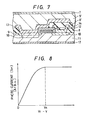
- a solid-state imaging device comprising a semiconductor integrated circuit in which a plurality of switching elements are disposed on a substrate, the switching elements being adapted for selecting positions of picture elements by turning “on” and “off” the switching elements in time sequence, suitably by means of scanners also disposed on the substrate; a photoconductive film which is disposed on the integrated circuit and which is connected to one end of each of the switching elements; and a light transmitting electrode which is disposed on the photoconductive film; characterised at least in that the breakdown voltage of a junction formed between the semiconductor substrate and a first impurity region which has a conductivity type opposite to that of the semiconductor substrate and which stores therein carriers attendant upon incidence of light is made smaller than the breakdown voltage between the first impurity region of said each switching element and a second impurity region thereof which forms a signal leading-out portion.
- a scanning circuit portion including a switching circuit etc. was produced on the semiconductor substrate by processes used for ordinary semiconductor devices.
- a thin SiO 2 film of approximately 800 g was formed on a p-type silicon substrate 11, and an Si 3 N 4 film of approximately 1,400 ⁇ was formed on predetermined positions of the SiO 2 film.
- a gate portion 12 of polycrystalline silicon and diffused regions 9 and 16 were formed, and an Si0 2 film was further formed thereon.
- an electrode lead-out opening for the impurity region 16 was provided by etching.
- An aluminium electrode 14 was evaporated to 8,000 ⁇ thickness, forming the line 10-1.
- an SiO 2 film 8' was formed to 7,500R.
- an electrode lead-out opening for the region 9 was provided by etching, and Al or Mo was evaporated to 1 ⁇ m thickness forming an electrode 13.
- the electrode 13 was formed to be so extensive to cover the regions 9 and 16 and the gate portion. This is because the incidence of light on signal processing regions between the picture elements is a cause of blooming and is undesirable.
- the manufacture of the semiconductor device portion described above may satisfactorily rely on the ordinary MOSIC manufacturing process as disclosed in, for example, the official gazette of Japanese Published Unexamined Patent Application No. 53-122316.
- the semiconductor body prepared by the steps thus far described was installed on a magnetron type sputtering equipment.
- An atmosphere of a mixed gas consisting of Ar and hydrogen was used and was under 0.2 Torr.
- the hydrogen content was 6 mol-%.
- silicon was used as a sputtering target.
- Reactive sputtering was carried out at a frequency of 13.56 MHz and an input power of 300W, to deposit a thin amorphous silicon film 5' containing hydrogen on the semiconductor body to a thickness of 500nm.
- the hydrogen content of the thin amorphous film was 20 atomic-%, and the resistivity thereof was 5x0 13 ⁇ .cm.
- the photoconductive film 5' is not restricted to this example. It may be any of various films, for example, an Se-As-Te film or a multilayered film consisting of layers of the components, and a two-element film of Zn-Se and Zn-Cd-Te.
- Table 1 sums up the parameters of the impurity concentration of the semi-conductor substrate 11 (boron was introduced by ion implantation), the channel length of the switching element, etc.
- Example Nos. 1-3 are examples of structures in which the high concentration impurity region was disposed only in the channel portion of the switch 4. In this case, the impurity concentration of the substrate was 1x10 15 /cm 3 . The depth of the high concentration impurity region sufficed to be approximately 0.05- 0.5pm.
- the impurity region 9 (and l6) had its impurity concentration made 10 19 - 10 20 /cm 3 and its diffusion depth made 0.5-1 ⁇ m.
Landscapes
- Solid State Image Pick-Up Elements (AREA)
- Transforming Light Signals Into Electric Signals (AREA)
Applications Claiming Priority (2)
| Application Number | Priority Date | Filing Date | Title |
|---|---|---|---|
| JP5756/80 | 1980-01-23 | ||
| JP575680A JPS56103578A (en) | 1980-01-23 | 1980-01-23 | Solid state pickup element |
Publications (3)
| Publication Number | Publication Date |
|---|---|
| EP0033230A2 true EP0033230A2 (de) | 1981-08-05 |
| EP0033230A3 EP0033230A3 (en) | 1983-06-08 |
| EP0033230B1 EP0033230B1 (de) | 1985-08-14 |
Family
ID=11619958
Family Applications (1)
| Application Number | Title | Priority Date | Filing Date |
|---|---|---|---|
| EP81300297A Expired EP0033230B1 (de) | 1980-01-23 | 1981-01-22 | Festkörper-Bildaufnahmevorrichtung |
Country Status (5)
| Country | Link |
|---|---|
| US (1) | US4405935A (de) |
| EP (1) | EP0033230B1 (de) |
| JP (1) | JPS56103578A (de) |
| CA (1) | CA1160374A (de) |
| DE (1) | DE3171759D1 (de) |
Cited By (5)
| Publication number | Priority date | Publication date | Assignee | Title |
|---|---|---|---|---|
| EP0029679A3 (en) * | 1979-11-14 | 1982-04-28 | Hitachi, Ltd. | Photoelectric device |
| EP0040076A3 (en) * | 1980-05-09 | 1982-09-22 | Hitachi, Ltd. | Photoelectric converter |
| DE3138314A1 (de) * | 1981-09-25 | 1983-04-14 | Siemens AG, 1000 Berlin und 8000 München | Zweidimensionaler halbleiter-bildsensor hoher packungsdichte mit fotoleiterschicht |
| DE3234044A1 (de) * | 1981-09-17 | 1983-04-21 | Matsushita Electric Industrial Co., Ltd., Kadoma, Osaka | Festkoerper-abbildungsvorrichtung |
| WO1986003057A1 (en) * | 1984-11-13 | 1986-05-22 | Eastman Kodak Company | A light sensing device |
Families Citing this family (7)
| Publication number | Priority date | Publication date | Assignee | Title |
|---|---|---|---|---|
| JPS57108363U (de) * | 1980-12-24 | 1982-07-03 | ||
| US4916505A (en) * | 1981-02-03 | 1990-04-10 | Research Corporation Of The University Of Hawaii | Composite unipolar-bipolar semiconductor devices |
| JPS5831670A (ja) * | 1981-08-20 | 1983-02-24 | Matsushita Electric Ind Co Ltd | 固体撮像装置 |
| JPS5848578A (ja) * | 1981-09-17 | 1983-03-22 | Matsushita Electric Ind Co Ltd | 固体撮像装置 |
| JPS58171850A (ja) * | 1982-03-31 | 1983-10-08 | Sony Corp | 固体撮像素子 |
| JPS6045057A (ja) * | 1983-08-23 | 1985-03-11 | Toshiba Corp | 固体撮像装置の製造方法 |
| US4885627A (en) * | 1988-10-18 | 1989-12-05 | International Business Machines Corporation | Method and structure for reducing resistance in integrated circuits |
Family Cites Families (4)
| Publication number | Priority date | Publication date | Assignee | Title |
|---|---|---|---|---|
| US4021844A (en) * | 1972-12-01 | 1977-05-03 | Thomson-Csf | Photosensitive diode array storage target |
| GB1595253A (en) * | 1977-01-24 | 1981-08-12 | Hitachi Ltd | Solid-state imaging devices |
| US4236829A (en) * | 1978-01-31 | 1980-12-02 | Matsushita Electric Industrial Co., Ltd. | Solid-state image sensor |
| JPS5822901B2 (ja) * | 1978-12-01 | 1983-05-12 | 株式会社日立製作所 | 固体撮像装置 |
-
1980
- 1980-01-23 JP JP575680A patent/JPS56103578A/ja active Pending
-
1981
- 1981-01-22 CA CA000369082A patent/CA1160374A/en not_active Expired
- 1981-01-22 EP EP81300297A patent/EP0033230B1/de not_active Expired
- 1981-01-22 DE DE8181300297T patent/DE3171759D1/de not_active Expired
- 1981-01-23 US US06/227,679 patent/US4405935A/en not_active Expired - Fee Related
Cited By (6)
| Publication number | Priority date | Publication date | Assignee | Title |
|---|---|---|---|---|
| EP0029679A3 (en) * | 1979-11-14 | 1982-04-28 | Hitachi, Ltd. | Photoelectric device |
| EP0040076A3 (en) * | 1980-05-09 | 1982-09-22 | Hitachi, Ltd. | Photoelectric converter |
| DE3234044A1 (de) * | 1981-09-17 | 1983-04-21 | Matsushita Electric Industrial Co., Ltd., Kadoma, Osaka | Festkoerper-abbildungsvorrichtung |
| DE3138314A1 (de) * | 1981-09-25 | 1983-04-14 | Siemens AG, 1000 Berlin und 8000 München | Zweidimensionaler halbleiter-bildsensor hoher packungsdichte mit fotoleiterschicht |
| WO1986003057A1 (en) * | 1984-11-13 | 1986-05-22 | Eastman Kodak Company | A light sensing device |
| US4633092A (en) * | 1984-11-13 | 1986-12-30 | Eastman Kodak Company | Light sensing device |
Also Published As
| Publication number | Publication date |
|---|---|
| JPS56103578A (en) | 1981-08-18 |
| EP0033230B1 (de) | 1985-08-14 |
| EP0033230A3 (en) | 1983-06-08 |
| CA1160374A (en) | 1984-01-10 |
| US4405935A (en) | 1983-09-20 |
| DE3171759D1 (en) | 1985-09-19 |
Similar Documents
| Publication | Publication Date | Title |
|---|---|---|
| US3403284A (en) | Target structure storage device using diode array | |
| US4148048A (en) | Solid-state imaging device | |
| US4873202A (en) | Solid state relay and method of manufacturing the same | |
| US4242694A (en) | Solid-state color imaging device | |
| US3576392A (en) | Semiconductor vidicon target having electronically alterable light response characteristics | |
| EP0033230B1 (de) | Festkörper-Bildaufnahmevorrichtung | |
| KR860000160B1 (ko) | 수광소자의 제조방법 | |
| US5084747A (en) | Photoelectric conversion device having cells of different spectral sensitivities | |
| EP0020175B2 (de) | Festkörper-Bildaufnahmevorrichtung | |
| EP0186162A2 (de) | Festkörperbildsensor | |
| US4796072A (en) | Solid-state imaging device with potential barriers between pixels | |
| US4695860A (en) | Gate structure for an integrated circuit comprising elements of the gate-insulator-semiconductor type and a method of fabrication of an integrated circuit using said structure | |
| EP0174133B1 (de) | Festkörper-Bildsensor | |
| JPH0120592B2 (de) | ||
| EP0502521B1 (de) | Festkörperbildaufnahmeanordnung und deren Herstellungsprozess | |
| GB1594185A (en) | Solid-state imaging devices | |
| EP0029679B1 (de) | Photoelektrische Vorrichtung | |
| US4499654A (en) | Method for fabricating semiconductor photodetector | |
| EP0031071B1 (de) | Festkörper-Bildaufnahmevorrichtung | |
| US5344794A (en) | Method of making a semiconductor chip | |
| CA1145835A (en) | Photoelectric device and method of producing the same | |
| EP0083060B1 (de) | Halbleiteranordnung mit Überspannungsschutzdiode | |
| US4536946A (en) | Method for fabricating semiconductor photodetector | |
| US4780765A (en) | Solid state image pick-up device | |
| USRE27775E (en) | Photoelectric induced i -n junction devices |
Legal Events
| Date | Code | Title | Description |
|---|---|---|---|
| PUAI | Public reference made under article 153(3) epc to a published international application that has entered the european phase |
Free format text: ORIGINAL CODE: 0009012 |
|
| 17P | Request for examination filed |
Effective date: 19810424 |
|
| AK | Designated contracting states |
Designated state(s): DE FR GB NL |
|
| RBV | Designated contracting states (corrected) |
Designated state(s): DE FR GB NL |
|
| PUAL | Search report despatched |
Free format text: ORIGINAL CODE: 0009013 |
|
| AK | Designated contracting states |
Designated state(s): DE FR GB NL |
|
| GRAA | (expected) grant |
Free format text: ORIGINAL CODE: 0009210 |
|
| AK | Designated contracting states |
Designated state(s): DE FR GB NL |
|
| REF | Corresponds to: |
Ref document number: 3171759 Country of ref document: DE Date of ref document: 19850919 |
|
| ET | Fr: translation filed | ||
| PLBE | No opposition filed within time limit |
Free format text: ORIGINAL CODE: 0009261 |
|
| STAA | Information on the status of an ep patent application or granted ep patent |
Free format text: STATUS: NO OPPOSITION FILED WITHIN TIME LIMIT |
|
| 26N | No opposition filed | ||
| PGFP | Annual fee paid to national office [announced via postgrant information from national office to epo] |
Ref country code: DE Payment date: 19930329 Year of fee payment: 13 |
|
| PGFP | Annual fee paid to national office [announced via postgrant information from national office to epo] |
Ref country code: GB Payment date: 19940112 Year of fee payment: 14 |
|
| PGFP | Annual fee paid to national office [announced via postgrant information from national office to epo] |
Ref country code: FR Payment date: 19940120 Year of fee payment: 14 |
|
| PGFP | Annual fee paid to national office [announced via postgrant information from national office to epo] |
Ref country code: NL Payment date: 19940131 Year of fee payment: 14 |
|
| PG25 | Lapsed in a contracting state [announced via postgrant information from national office to epo] |
Ref country code: DE Effective date: 19941001 |
|
| PG25 | Lapsed in a contracting state [announced via postgrant information from national office to epo] |
Ref country code: GB Effective date: 19950122 |
|
| PG25 | Lapsed in a contracting state [announced via postgrant information from national office to epo] |
Ref country code: NL Effective date: 19950801 |
|
| GBPC | Gb: european patent ceased through non-payment of renewal fee |
Effective date: 19950122 |
|
| PG25 | Lapsed in a contracting state [announced via postgrant information from national office to epo] |
Ref country code: FR Effective date: 19950929 |
|
| NLV4 | Nl: lapsed or anulled due to non-payment of the annual fee |
Effective date: 19950801 |
|
| REG | Reference to a national code |
Ref country code: FR Ref legal event code: ST |