EP0033634A2 - Thermischer Registrierkopf - Google Patents
Thermischer Registrierkopf Download PDFInfo
- Publication number
- EP0033634A2 EP0033634A2 EP81300374A EP81300374A EP0033634A2 EP 0033634 A2 EP0033634 A2 EP 0033634A2 EP 81300374 A EP81300374 A EP 81300374A EP 81300374 A EP81300374 A EP 81300374A EP 0033634 A2 EP0033634 A2 EP 0033634A2
- Authority
- EP
- European Patent Office
- Prior art keywords
- drive circuits
- shift register
- thermal
- resistive elements
- terminals
- Prior art date
- Legal status (The legal status is an assumption and is not a legal conclusion. Google has not performed a legal analysis and makes no representation as to the accuracy of the status listed.)
- Granted
Links
Images


Classifications
-
- H—ELECTRICITY
- H04—ELECTRIC COMMUNICATION TECHNIQUE
- H04N—PICTORIAL COMMUNICATION, e.g. TELEVISION
- H04N1/00—Scanning, transmission or reproduction of documents or the like, e.g. facsimile transmission; Details thereof
- H04N1/40—Picture signal circuits
- H04N1/40025—Circuits exciting or modulating particular heads for reproducing continuous tone value scales
- H04N1/40031—Circuits exciting or modulating particular heads for reproducing continuous tone value scales for a plurality of reproducing elements simultaneously
-
- G—PHYSICS
- G06—COMPUTING OR CALCULATING; COUNTING
- G06K—GRAPHICAL DATA READING; PRESENTATION OF DATA; RECORD CARRIERS; HANDLING RECORD CARRIERS
- G06K15/00—Arrangements for producing a permanent visual presentation of the output data, e.g. computer output printers
- G06K15/02—Arrangements for producing a permanent visual presentation of the output data, e.g. computer output printers using printers
- G06K15/028—Arrangements for producing a permanent visual presentation of the output data, e.g. computer output printers using printers by thermal printers
-
- H—ELECTRICITY
- H04—ELECTRIC COMMUNICATION TECHNIQUE
- H04N—PICTORIAL COMMUNICATION, e.g. TELEVISION
- H04N1/00—Scanning, transmission or reproduction of documents or the like, e.g. facsimile transmission; Details thereof
- H04N1/024—Details of scanning heads ; Means for illuminating the original
- H04N1/032—Details of scanning heads ; Means for illuminating the original for picture information reproduction
Definitions
- This invention relates to a thermal recording head for a thermal recording apparatus and, more particularly, to a thermal recording head having drive circuits and a shift register for supplying picture signals in parallel to thermal'resistive elements on an insulated substrate.
- the incoming picture signals are received in serial form by the shift register, converted to parallel signals and supplied to the drive circuits which drive the thermal resistive elements.
- thermal recording techniques are used in many fields because of easy maintenance and low cost.
- thermal resistive elements are placed in a line and a thermal sensitive paper is passed over the line of elements.
- the thermal resistive elements are selectively heated to record the image on the thermal sensitive paper.
- matrix circuits are used to decrease the number of lead lines and drive circuits.
- the matrix circuits are circuits that supply picture signals to separate groups of thermal resistive elements over parallel lead lines.
- the matrix circuits select one of these groups at a time.
- the total number of lead lines to each group is more than the number of thermal resistive elements in one group.
- a thermal recording head is disclosed in Japanese patent disclosures Nos. 54-48562 and 54-56320 in which shift registers convert incoming serial signals into parallel signals.
- T m.t
- t the time necessary to actuate one element
- m the number of groups of thermal resistive elements.
- thermal heads are disclosed in Japanese patent disclosures Nos. 52-105840 and 53-13434. These thermal heads have memory elements associated with each thermal resistive element to store the picture signal so all thermal resistive elements can be actuated at the same time. The picture signals are successively supplied in parallel to each group of memory elements at high speed and then the line of thermal resistive elements is actuated by all groups of memory elements at the same time.
- these thermal heads require a number of lead lines which is greater than the number of thermal resistive elements of one group.
- these thermal heads require a number of memory elements, which number is the same as the number of thermal resistive elements, and a switch having large current capacity.
- the thermal recording head includes an insulated substrate, a plurality of thermal resistive elements in line on the insulated substrate, a plurality of drive circuits having signal input terminals, current supply terminals and output terminals, each output terminal of the drive circuits being connected to each thermal resistive element.
- a shift register having a plurality of memory units, the number of which is the same as the number of thermal resistive elements, receives the input signals. Each memory unit is connected to each signal input terminal of the drive circuits.
- the shift register receives serial input signals and supplies picture signals to the drive circuits in parallel.
- a metal cover is placed on the insulated substrate to cover the shift register and the drive circuits. The metal cover is connected to the current supply terminals of the drive circuits.
- this invention is suitable for thermal recording apparatus in which all the desired thermal resistive elements can be driven at the same time (e.g., recording apparatus for facsimile signals).
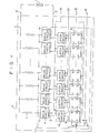
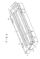
- Figs. 1 and 2 show a wiring diagram and a perspective view of one embodiment of the thermal recording head of this invention.
- a plurality of thermal resistive elements 1 are placed in line on an insulated substrate 2 shown as a dash and dot line in Fig. 1. The ends of each thermal resistive element 1 are connected in common by a current supply bus L.
- a metal cover 3 covers a plurality of drive circuits 4, latch circuits 14 and a shift register 8.
- Metal cover 3 has two functions: one function is to hermetically seal the electrical circuits and another function is to act as a large current supply bus. For example, metal cover 3 is 20 cm long, 3 cm wide and 0.5 mm thick. The resistance of metal cover 3 is about 0.3 mohms.
- Metal cover 3 is shown as a dash and two dots line in Fig. 1. Insulated substrate 2, which radiates heat, is fixed on a metal plate 20 by clamps 21, 22, 23 and 24.
- each drive circuit 4 independently drive thermal resistive elements 1 according to the incoming picture signals.
- each drive circuit 4 includes a switching element having a signal input terminal (S), a current supply terminal (C) and an output terminal (O).
- Output terminals (0) are connected to the other ends of thermal resistive elements 1 and all current supply terminals (C) are connected to a common current terminal 5 through metal cover 3.
- an external D.C. power source 7 is connected between current terminal 5 and source terminal 6 of current supply bus L as shown in Fig. 1.
- Shift register 8 has a plurality of memory units (M) (e.g., flip-flops), the number of which is the same as the number of thermal resistive elements 1 (e.g., 1,728 bits). In this embodiment, these memory units (M) are serially connected. Shift register 8 receives serial picture signals from a signal input line connected to input terminal 9 via inverters 10 and 11. The picture signals are transferred or shifted through the shift register in accordance with clock signals input at clock terminal 12; the picture signals are stored in the memory units (M).
- M memory units
- each latch circuit 14 has gate terminal (G) controlled by a drive signal from terminal 15; upon receipt of the drive signal, all the latch circuits 14 output their content ("0" or "1") to their respective drive circuits 4.
- the drive circuits 4 which receive a ("1") from latch circuits 14 are activated and the switching element in each of these drive circuits, is turned on to actuate the desired thermal resistive elements 1.
- a thermal sensitive paper (not shown) is moved across the thermal resistive elements and the heated or actuated thermal resistive elements turn the corresponding portions of the thermal sensitive paper black.
- the drive signal at terminal 15 is supplied when it is desired to record (e.g., for a duration of 1-4 msec.). When the drive signal terminates, current does not flow in thermal resistive elements 1. When the recording of one line is finished, the thermal sensitive paper moves a predetermined distance and the recording of the next line is executed.
- current terminal 5, and all the current supply terminals (C) of drive circuits 4 are connected to metal cover 3. Therefore, even if almost all of the drive circuits 4 must be activated, it is possible to supply sufficient current to each drive circuit.
- insulated substrate 2 is fixed on a metal plate by metal clamps 23 and 24 for radiating heat generated by the current flow in metal cover 3. Therefore, the heat generated by large current can be sufficiently radiated.
- the length of one line is 1,728 bits and the electrical circuit covered by metal cover 3 is constructed of C 2 M OS. If the frequency of transfer clock signal is 1 MHz, the transfer time of one line is 1.728 msec. and if the frequency is 3 MHz, the transfer time is 0.576 msec. Thus, it is possible to use high speed TTL integrated circuits as shift register 8. However, use of these integrated circuits is undesirable because they generate heat.
- the current supply bus L is constructed of thin metal film and thick Cu film. The thick Cu film can be formed by galvanizing or it can be fixed beforehand on the thin film by pewter or conductive epoxy.
- the latch circuits 14 are divided into a plurality of groups (e.g., m groups).
- the latch circuits of each group are connected terminals 15 1 , 15 2 , ... 15 m by gate terminals (G) connected in common as shown in Fig. 3.
- Each group 14 1 , 14 2 , ..14 m of the latch circuits can be independently operated by respectively supplying drive signals to gate terminals over terminals 15.
- a power source 7 having small capacity can be used because all the drive circuits in each group are activated in accordance with each group of latch circuits 14 1 , 14 2 , ... 14 m by supplying drive signals to terminals 15 1 , 15 2 , ... 15 m in order.
- the drive signals are supplied to these terminals 15 1 , 15 2 , ,.. 15 m in accordance with picture signals supplied to input terminal 9. Namely, in case the picture signals of one line have only a few black signals ("1"), drive signals are supplied to terminals 15 1 . 15 2 , ... 15 m at the same time. When picture signals of one line have many black signals, drive signals are selectively supplied to terminals 15. Thus, it is possible to increase recording speed without using a power source having large capacity.
- FIG. 4 Another embodiment of this invention is shown in Fig. 4.
- a plurality of shift registers 8 1 , 8 2 , ... 8 n are used.
- Input terminals 9 1 , 9 2 , ... 9 n and inverters 10 1 , 10 2 , ... 10 n , and 11 1 , 11 2 , ... 11 n are connected to every shift register 8.
- the previous embodiments required a relatively long time to input picture signals of one line because all memory units of shift register 8 are connected in series.
- a relatively short time is required because picture signals of one line can be supplied separately.
- the time for supplying picture signals becomes 1/n in comparison with the previous embodiments.
- a plurality of either terminals 15 or input (picture signal) terminals 9 are needed; therefore, the number of lead lines increases.
- the number of lead lines is m or n, which is still less than the number used in known systems.
- metal plate 20 is connected to current supply bus L via metal clamps 21 and 22.
- current supply bus L is grounded and positive voltage is supplied to current terminal 5.
- the source terminal 6 is not necessary because metal plate 20 can be grounded.
- insulated substrate 2 is fixed on a metal plate.
- this metal plate is not necessary as shown in Fig. 6 where a power source is connected between current terminal 5 and source terminal 6.
- latch circuits having gate terminals are used.
- drive circuits having a gate function can be used instead.
- ring counters, memories, charge coupled devices, etc. instead of a shift register.
Landscapes
- Engineering & Computer Science (AREA)
- Multimedia (AREA)
- Signal Processing (AREA)
- General Engineering & Computer Science (AREA)
- Physics & Mathematics (AREA)
- General Physics & Mathematics (AREA)
- Theoretical Computer Science (AREA)
- Electronic Switches (AREA)
- Facsimile Heads (AREA)
Applications Claiming Priority (2)
| Application Number | Priority Date | Filing Date | Title |
|---|---|---|---|
| JP1027380A JPS56106883A (en) | 1980-01-31 | 1980-01-31 | Thermal head |
| JP10273/80 | 1980-01-31 |
Publications (3)
| Publication Number | Publication Date |
|---|---|
| EP0033634A2 true EP0033634A2 (de) | 1981-08-12 |
| EP0033634A3 EP0033634A3 (en) | 1982-03-31 |
| EP0033634B1 EP0033634B1 (de) | 1984-05-09 |
Family
ID=11745702
Family Applications (1)
| Application Number | Title | Priority Date | Filing Date |
|---|---|---|---|
| EP81300374A Expired EP0033634B1 (de) | 1980-01-31 | 1981-01-28 | Thermischer Registrierkopf |
Country Status (5)
| Country | Link |
|---|---|
| US (1) | US4369452A (de) |
| EP (1) | EP0033634B1 (de) |
| JP (1) | JPS56106883A (de) |
| CA (1) | CA1162590A (de) |
| DE (1) | DE3163433D1 (de) |
Cited By (3)
| Publication number | Priority date | Publication date | Assignee | Title |
|---|---|---|---|---|
| EP0079063A3 (en) * | 1981-11-06 | 1985-06-19 | Matsushita Electric Industrial Co., Ltd. | Thermal printing head |
| EP0113052A3 (de) * | 1982-12-30 | 1985-10-30 | International Business Machines Corporation | Wärmeübertragungsdruckkopf |
| EP0088487A3 (en) * | 1982-01-19 | 1986-10-29 | Fujitsu Limited | Semiconductor device, e.g. for controlling a thermal printing head |
Families Citing this family (11)
| Publication number | Priority date | Publication date | Assignee | Title |
|---|---|---|---|---|
| JPS5812776A (ja) * | 1981-07-17 | 1983-01-24 | Fuji Xerox Co Ltd | サ−マルヘツド駆動方法 |
| JPS58138664A (ja) * | 1982-02-12 | 1983-08-17 | Fuji Xerox Co Ltd | 感熱記録ヘツド駆動装置 |
| JPS5938053U (ja) * | 1982-08-31 | 1984-03-10 | 三菱電機株式会社 | サ−マルプリントヘツド |
| US4590484A (en) * | 1983-01-13 | 1986-05-20 | Ricoh Company, Ltd. | Thermal recording head driving control system |
| JPS59227471A (ja) * | 1983-06-09 | 1984-12-20 | Matsushita Electric Ind Co Ltd | 感熱記録用ヘツド |
| JPS6072756A (ja) * | 1983-09-30 | 1985-04-24 | Ishida Scales Mfg Co Ltd | 発熱ヘツドの制御回路 |
| JP2630960B2 (ja) * | 1987-10-17 | 1997-07-16 | グラフテック株式会社 | サーマルドットアレイを用いた波形記録装置 |
| JPH059616Y2 (de) * | 1987-10-17 | 1993-03-10 | ||
| US4912483A (en) * | 1987-10-22 | 1990-03-27 | Graphtec Kabushiki Kaisha | Balanced head suspension in thermal recorders |
| JP2508810B2 (ja) * | 1988-06-29 | 1996-06-19 | 三菱電機株式会社 | サ―マルヘッド |
| US4954839A (en) * | 1989-07-24 | 1990-09-04 | Cryptek, Inc. | Self-aligning print head assembly with advanced shielding characteristics |
Family Cites Families (14)
| Publication number | Priority date | Publication date | Assignee | Title |
|---|---|---|---|---|
| US3515850A (en) * | 1967-10-02 | 1970-06-02 | Ncr Co | Thermal printing head with diffused printing elements |
| JPS4822228U (de) * | 1971-07-20 | 1973-03-14 | ||
| US3903393A (en) * | 1973-07-30 | 1975-09-02 | Tektron Inc | Thermal printing head |
| US4022665A (en) * | 1974-12-09 | 1977-05-10 | Institute Of Gas Technology | Two phase anaerobic digestion |
| US3953708A (en) * | 1975-04-25 | 1976-04-27 | Xerox Corporation | Thermal printer using amorphous semiconductor devices |
| US4067801A (en) * | 1975-05-14 | 1978-01-10 | Hitachi, Ltd. | Process and system for anaerobic treatment of biochemical waste |
| JPS599069B2 (ja) * | 1975-11-19 | 1984-02-29 | 株式会社日立製作所 | 多重マトリクス液晶パネルの駆動方法 |
| CH621715A5 (en) * | 1976-04-01 | 1981-02-27 | Pierre Morel | Process for recycling waste, especially household rubbish |
| JPS5838140B2 (ja) * | 1976-06-10 | 1983-08-20 | 日清製粉株式会社 | 麺類の製造方法およびその装置 |
| JPS5339140A (en) * | 1976-09-22 | 1978-04-10 | Nippon Telegr & Teleph Corp <Ntt> | Head drive system |
| US4141018A (en) * | 1976-11-08 | 1979-02-20 | Tokyo Shibaura Electric Co., Ltd. | Thermal recording head and drive circuit |
| US4224869A (en) * | 1977-06-28 | 1980-09-30 | Enertec | Parallel line printer |
| JPS5448562A (en) * | 1977-07-30 | 1979-04-17 | Nippon Telegr & Teleph Corp <Ntt> | Recording head |
| SE7802501L (sv) * | 1978-03-06 | 1979-09-07 | A Betong Ab | Forfarande for metangasframstellning och anordning for genomforande av forfarandet |
-
1980
- 1980-01-31 JP JP1027380A patent/JPS56106883A/ja active Granted
-
1981
- 1981-01-26 US US06/228,671 patent/US4369452A/en not_active Expired - Lifetime
- 1981-01-28 DE DE8181300374T patent/DE3163433D1/de not_active Expired
- 1981-01-28 EP EP81300374A patent/EP0033634B1/de not_active Expired
- 1981-01-30 CA CA000369778A patent/CA1162590A/en not_active Expired
Cited By (3)
| Publication number | Priority date | Publication date | Assignee | Title |
|---|---|---|---|---|
| EP0079063A3 (en) * | 1981-11-06 | 1985-06-19 | Matsushita Electric Industrial Co., Ltd. | Thermal printing head |
| EP0088487A3 (en) * | 1982-01-19 | 1986-10-29 | Fujitsu Limited | Semiconductor device, e.g. for controlling a thermal printing head |
| EP0113052A3 (de) * | 1982-12-30 | 1985-10-30 | International Business Machines Corporation | Wärmeübertragungsdruckkopf |
Also Published As
| Publication number | Publication date |
|---|---|
| JPS6221469B2 (de) | 1987-05-13 |
| CA1162590A (en) | 1984-02-21 |
| US4369452A (en) | 1983-01-18 |
| EP0033634A3 (en) | 1982-03-31 |
| EP0033634B1 (de) | 1984-05-09 |
| DE3163433D1 (en) | 1984-06-14 |
| JPS56106883A (en) | 1981-08-25 |
Similar Documents
| Publication | Publication Date | Title |
|---|---|---|
| US4369452A (en) | Thermal recording head | |
| EP0079063B1 (de) | Thermischer Druckkopf | |
| US4141018A (en) | Thermal recording head and drive circuit | |
| EP0141880B1 (de) | Aufzeichnungsgerät | |
| US4415907A (en) | Printing pulse control circuit for thermal printing head | |
| GB2104266A (en) | Control of a light emitting diode array | |
| US4532523A (en) | Tone control for thermal ink-transfer printing apparatus | |
| GB1595394A (en) | Power supply control arrangements | |
| EP0061314B1 (de) | Wärmeempfindliches Aufzeichnungsgerät | |
| EP0053895B1 (de) | Thermischer Kopf für Faksimiledrucker | |
| USRE32897E (en) | Thermal print head | |
| US3122996A (en) | heatwole | |
| EP0215434A1 (de) | Bilderzeugungsgerät | |
| US4287521A (en) | CRT Hard copy apparatus with multi-directional sampling and printing | |
| US4361844A (en) | Recording head | |
| US3343130A (en) | Selection matrix line capacitance recharge system | |
| EP0381282B1 (de) | Verfahren und Gerät für bildweise Belichtung einer lichtempfindlichen Vorlage unter Verwendung einer Anzahl von Lichtventilen | |
| US3927365A (en) | Switch operating device | |
| US3082330A (en) | Generating arbitrary varying-amplitude step-wave using distributor having separate channel individual to each successive step | |
| US3185080A (en) | Hammer magnet gate system in high speed printers using transistor circuits | |
| JP3066658B2 (ja) | 画像読取り装置 | |
| US4673952A (en) | Driving device for a thermal element | |
| GB1025487A (en) | Improvements in asynchronous page-at-a-time printers | |
| JPS60259050A (ja) | サーマルヘツド | |
| GB2154776A (en) | Control of a light emitting diode array |
Legal Events
| Date | Code | Title | Description |
|---|---|---|---|
| PUAI | Public reference made under article 153(3) epc to a published international application that has entered the european phase |
Free format text: ORIGINAL CODE: 0009012 |
|
| 17P | Request for examination filed |
Effective date: 19810202 |
|
| AK | Designated contracting states |
Designated state(s): DE FR GB IT NL |
|
| PUAL | Search report despatched |
Free format text: ORIGINAL CODE: 0009013 |
|
| AK | Designated contracting states |
Designated state(s): DE FR GB IT NL |
|
| ITF | It: translation for a ep patent filed | ||
| GRAA | (expected) grant |
Free format text: ORIGINAL CODE: 0009210 |
|
| AK | Designated contracting states |
Designated state(s): DE FR GB IT NL |
|
| PG25 | Lapsed in a contracting state [announced via postgrant information from national office to epo] |
Ref country code: NL Effective date: 19840509 |
|
| REF | Corresponds to: |
Ref document number: 3163433 Country of ref document: DE Date of ref document: 19840614 |
|
| ET | Fr: translation filed | ||
| RAP2 | Party data changed (patent owner data changed or rights of a patent transferred) |
Owner name: KABUSHIKI KAISHA TOSHIBA |
|
| NLV1 | Nl: lapsed or annulled due to failure to fulfill the requirements of art. 29p and 29m of the patents act | ||
| REG | Reference to a national code |
Ref country code: FR Ref legal event code: CD |
|
| PLBE | No opposition filed within time limit |
Free format text: ORIGINAL CODE: 0009261 |
|
| STAA | Information on the status of an ep patent application or granted ep patent |
Free format text: STATUS: NO OPPOSITION FILED WITHIN TIME LIMIT |
|
| 26N | No opposition filed | ||
| REG | Reference to a national code |
Ref country code: GB Ref legal event code: 746 |
|
| ITTA | It: last paid annual fee | ||
| REG | Reference to a national code |
Ref country code: FR Ref legal event code: D6 |
|
| PGFP | Annual fee paid to national office [announced via postgrant information from national office to epo] |
Ref country code: DE Payment date: 19991231 Year of fee payment: 20 |
|
| PGFP | Annual fee paid to national office [announced via postgrant information from national office to epo] |
Ref country code: FR Payment date: 20000112 Year of fee payment: 20 |
|
| PGFP | Annual fee paid to national office [announced via postgrant information from national office to epo] |
Ref country code: GB Payment date: 20000126 Year of fee payment: 20 |
|
| REG | Reference to a national code |
Ref country code: FR Ref legal event code: ER Free format text: ERRATUM: LICENCE OF RIGHT ACCEPTED |
|
| PG25 | Lapsed in a contracting state [announced via postgrant information from national office to epo] |
Ref country code: GB Free format text: LAPSE BECAUSE OF EXPIRATION OF PROTECTION Effective date: 20010127 |
|
| REG | Reference to a national code |
Ref country code: GB Ref legal event code: PE20 Effective date: 20010127 |