EP0034465A2 - Adressenpufferschaltung - Google Patents
Adressenpufferschaltung Download PDFInfo
- Publication number
- EP0034465A2 EP0034465A2 EP81300566A EP81300566A EP0034465A2 EP 0034465 A2 EP0034465 A2 EP 0034465A2 EP 81300566 A EP81300566 A EP 81300566A EP 81300566 A EP81300566 A EP 81300566A EP 0034465 A2 EP0034465 A2 EP 0034465A2
- Authority
- EP
- European Patent Office
- Prior art keywords
- buffer circuit
- address
- output terminals
- address buffer
- circuit
- Prior art date
- Legal status (The legal status is an assumption and is not a legal conclusion. Google has not performed a legal analysis and makes no representation as to the accuracy of the status listed.)
- Granted
Links
Images

Classifications
-
- H—ELECTRICITY
- H03—ELECTRONIC CIRCUITRY
- H03K—PULSE TECHNIQUE
- H03K19/00—Logic circuits, i.e. having at least two inputs acting on one output; Inverting circuits
- H03K19/02—Logic circuits, i.e. having at least two inputs acting on one output; Inverting circuits using specified components
- H03K19/08—Logic circuits, i.e. having at least two inputs acting on one output; Inverting circuits using specified components using semiconductor devices
- H03K19/094—Logic circuits, i.e. having at least two inputs acting on one output; Inverting circuits using specified components using semiconductor devices using field-effect transistors
- H03K19/09425—Multistate logic
-
- G—PHYSICS
- G11—INFORMATION STORAGE
- G11C—STATIC STORES
- G11C11/00—Digital stores characterised by the use of particular electric or magnetic storage elements; Storage elements therefor
- G11C11/21—Digital stores characterised by the use of particular electric or magnetic storage elements; Storage elements therefor using electric elements
- G11C11/34—Digital stores characterised by the use of particular electric or magnetic storage elements; Storage elements therefor using electric elements using semiconductor devices
- G11C11/40—Digital stores characterised by the use of particular electric or magnetic storage elements; Storage elements therefor using electric elements using semiconductor devices using transistors
- G11C11/41—Digital stores characterised by the use of particular electric or magnetic storage elements; Storage elements therefor using electric elements using semiconductor devices using transistors forming static cells with positive feedback, i.e. cells not needing refreshing or charge regeneration, e.g. bistable multivibrator or Schmitt trigger
- G11C11/413—Auxiliary circuits, e.g. for addressing, decoding, driving, writing, sensing, timing or power reduction
- G11C11/417—Auxiliary circuits, e.g. for addressing, decoding, driving, writing, sensing, timing or power reduction for memory cells of the field-effect type
- G11C11/418—Address circuits
-
- G—PHYSICS
- G11—INFORMATION STORAGE
- G11C—STATIC STORES
- G11C8/00—Arrangements for selecting an address in a digital store
-
- G—PHYSICS
- G11—INFORMATION STORAGE
- G11C—STATIC STORES
- G11C8/00—Arrangements for selecting an address in a digital store
- G11C8/06—Address interface arrangements, e.g. address buffers
-
- H—ELECTRICITY
- H03—ELECTRONIC CIRCUITRY
- H03K—PULSE TECHNIQUE
- H03K19/00—Logic circuits, i.e. having at least two inputs acting on one output; Inverting circuits
- H03K19/02—Logic circuits, i.e. having at least two inputs acting on one output; Inverting circuits using specified components
- H03K19/08—Logic circuits, i.e. having at least two inputs acting on one output; Inverting circuits using specified components using semiconductor devices
- H03K19/094—Logic circuits, i.e. having at least two inputs acting on one output; Inverting circuits using specified components using semiconductor devices using field-effect transistors
- H03K19/09425—Multistate logic
- H03K19/09429—Multistate logic one of the states being the high impedance or floating state
Definitions
- This invention relates to an address buffer circuit.
- a memory cell is in general selected in accordance with outputs of row and column address decoders.
- These address decoders are generally composed of NOR gates and to these NOR gates there are supplied .specified signals from amongst in-phase internal address signals and inverse-phase internal address signals which internal address signals are generated, in address buffer circuits, from an external address input.
- address buffer circuits are often designed so that power consumption by such address buffer circuits is suspended during stand-by periods in response to a signal generated from a external chip select input signal.
- output timing depends upon the relationship between an external chip select input signal and an external address input signal, and output timing differs when the external chip select input signal and the external address input signal bear different relationships. Differences in output timing are generally very short periods which do not cause any problems when chip select access is faster than address access, but when chip select access is slower than address access because of the circuit design, the differences can give rise to a slower access time for a memory.
- an address buffer circuit operable to receive an address input signal, and operable in an active period to provide, at respective output terminals of the buffer circuit, a pair of mutually complementary output signals of levels dependent upon the address input signal, having means operable in a stand-by period, designated by a signal external of the buffer circuit, to cut power consumption by the buffer circuit, characterised in that a short circuit means is connected between the respective output terminals,which means is operable to set the potentials of the output terminals in a stand-by period to a level between high and low levels of the output terminals in an active period,by electrically connecting the output terminals.
- An embodiment of the present invention can provide an address buffer circuit which does not suffer the disadvantage mentioned above and which assure s high speed operation.
- An embodiment of this invention can provide an address buffer circuit of a simple structure.
- An embodiment of tbepresent invention provides, for example, an address buffer circuit formed so that the power consumption in the circuit is suspended by an external signal during a stand-by period, a so-called power down type address buffer circuit, and so that a pair of complementary outputs are provided from the buffer circuit in correspondence to an address input signal, in which address buffer circuit a short circuit means, which becomes ON during such a stand-by period, is provided between complementary output terminals at an output stage. of the buffer circuit and in which the level of the complementary output terminals during such a stand-by period is selected to be a level intermediate between the high and low levels respectively of the output terminals during an active period.
- Figure 1 illustrates a power-down type address buffer circuit embodying the present invention.
- depletion type MOS transistors T 4 to T 6 and enhancement type MOS transistors Tg to T 11 form three invertor stages I 1 to I 3
- depletion type MOS transistors T 7 , T 8 and enhancement type MOS transistors T 12 , T 13 form a push-pull output stage circuit PP.
- the three invertor stages I 1 to 1 3 effect successive inversions of an external address input A in .
- An output of second invertor stage I 2 is applied to the respective gates of transistors T 7 , T 13 of the push-pull circuit PP, whilst an output of the third invertor stage I3 is applied to the gates of transistors T 12 , T 8 of circuit PP.
- an internal address signal A which is in-phase with the external address input A in and an internal address signal AB which has a phase the inverse of that of the signal A in can beobtained at complementary output terminals N 1 , N 2 of the push-pull circuit PP.
- Transistors T 1 to T 3 connected between the invertor stages I 1 to 1 3 and power source V cc are power-down transistors. These transistors become OFF when an internal chip select signal CSO, which is inverted in phase with respect to an external chip select signal, becomes "L" level during a standby period, thus disconnecting power supply from invertor stages I 1 to I 3 .
- transistors T14, T 15 connected between the gates of transistors of push-pull circuit PP and ground potential GND are also power-down transistors. These transistors turn ON when an internal chip select signal CS2B, which is in-phase with the external chip select signal, becomes "H".level during a stand-by period, thus forcibly pulling the gates of transistors T 7 , T 8 , T 12 and T 13 to ground potential.
- FIG. 2 illustrates a circuit for generating internal chip select signals CSO and CS2B.
- T 17 to T 20 are depletion type load MOS transistors, while T 21 to T 24 are enhancement type drive transistors. These transistors form two invertor stages I 4 , I 5 and three invertor stages I 4 , I 6 and I 7 .
- an external input signal CS is applied to the first invertor stage I 4 the signal CS2B which is in-phase with the external input is obtained from the second invertor stage I 5 , and the signal CSO which has a phase the inverse of the external input is obtained through the invertor stages I4, I 6 and I 7 .
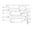
- the external chip select input signal CS for the circuit shown in Figure 2 is of different levels in a stand-by period STB and an active period ACT as shown in Figure 3A.
- the complementary outputs A, AB of the push-pull circuit PP change in different manners as shown respectively in Figures 3C and 3E when the external address input A in to the circuit of Figure 1 changes in respective different manners as shown in Figures 3B and 3D.
- Figure 3B illustrates a cases in which a change of external address input A in occurs at a timing at which the external chip select input CS enters the stand-by mode.
- the address buffer circuit of Figure 1 is operated by internal chip select signals CSO and CS2B which are delayed a little from the external chip select input signal CS, the internal signals CSO, CS2B are still at levels corresponding to an active condition (CSO is "H", while CS2B is "L") when the external signal CS has become “H”, and the address buffer circuit continues operation until the internal signals CSO and CS2B achieve stand-by levels (e.g. the levels of A and AB start to change to follow up the change in A in in the case of Figure 3C until CSO and CS2B achieve stand-by levels).
- stand-by levels e.g. the levels of A and AB start to change to follow up the change in A in in the case of Figure 3C until CSO and CS2B achieve stand-by levels.
- a depletion type transistor (T 7 or T 8 ) could provide an output of a level almost as high as power source voltage (V cc ), but when gate potential is equal to ground potential GND, as in the present case, the depletion type transistors cannot provide such a high output level but rather provide a level as indicated in Figure 3C.
- the internal address outputs A, AB begin changing from the immediately preceding levels L 1 , L 2 .
- the signal A falls to ground potential GND from level L 1
- the inverted signal AB increases to V cc from level L 2 .
- This level L 3 is gradually reduced as a result of junction leakage etc., but such variation cannot be expected to have any significant effect in a case in which a transistor operates over a short cycle.
- the input stage of an address decoder (not illustrated) comprises a NOR gate which receives a plurality of in-phase and inverted-phase address signals as inputs thereto and its speed of operation is determined by the changes of inputs thereto between "H" and "L” levels. Therefore, when selecting in row or column directions, a time difference corresponding to T 0 is generated in the course of operations as indicated in Figures 3. This time difference T 0 is generally very small and does not give rise to a problem, as mentioned above, when chip select access is faster than address access. However, if chip select access is slower than address access as a result of circuit design, access to memory is delayed by the time difference T 0 explained above.
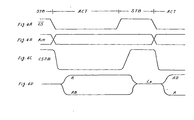
- short circuit means consisting of an enhancement type MOS transistor T 16 , is connected as shown in Figure 1 between the complementary output terminals N 1 , N 2 of the push-pull circuit PP at the output stage of an address buffer circuit.
- This short circuit means is controlled by the internal chip select signal CS2B which is in-phase with the external chip select signal. For this reason, the transistor T 16 becomes OFF in an active period ACT and thereby completely isolates the complementary output terminals N 1 , N 2 from one another and has no effect on the outputs A, AB, but becomes ON in a stand-by period STB, electrically connecting the terminals N 1 and N 2 .
- Figures 4A to 4D illustrate operating waveforms of the circuit of Figure 1 where the transistor T 16 is provided.
- Figures 4A and 4B correspond to Figures 3A and 3D
- Figure 4C illustrates the behaviour of CS2B
- Figure 4D illustrates the behaviour of A and AB.
- an address buffer circuit embodying this invention provides a pair of complementary signals, for example for selecting a memory cell of a memory device, according to an address input signal supplied to the buffer circuit.
- the address buffer circuit comprises short circuit means connected between the two output terminals from which the complementary signals are respectively provided. During a stand-by period of the memory device the short circuit means electrically connects the two output terminals so that the potentials of the two terminals achieve a common level intermediate between high and low levels provided at the output terminals during an active period of the memory device.
Landscapes
- Engineering & Computer Science (AREA)
- Microelectronics & Electronic Packaging (AREA)
- Computer Hardware Design (AREA)
- Power Engineering (AREA)
- Physics & Mathematics (AREA)
- Computing Systems (AREA)
- General Engineering & Computer Science (AREA)
- Mathematical Physics (AREA)
- Static Random-Access Memory (AREA)
Applications Claiming Priority (2)
| Application Number | Priority Date | Filing Date | Title |
|---|---|---|---|
| JP18018/80 | 1980-02-16 | ||
| JP55018018A JPS5842558B2 (ja) | 1980-02-16 | 1980-02-16 | アドレス バッファ回路 |
Publications (3)
| Publication Number | Publication Date |
|---|---|
| EP0034465A2 true EP0034465A2 (de) | 1981-08-26 |
| EP0034465A3 EP0034465A3 (en) | 1983-07-20 |
| EP0034465B1 EP0034465B1 (de) | 1985-11-21 |
Family
ID=11959921
Family Applications (1)
| Application Number | Title | Priority Date | Filing Date |
|---|---|---|---|
| EP81300566A Expired EP0034465B1 (de) | 1980-02-16 | 1981-02-12 | Adressenpufferschaltung |
Country Status (5)
| Country | Link |
|---|---|
| US (1) | US4393480A (de) |
| EP (1) | EP0034465B1 (de) |
| JP (1) | JPS5842558B2 (de) |
| DE (1) | DE3172937D1 (de) |
| IE (1) | IE50732B1 (de) |
Families Citing this family (4)
| Publication number | Priority date | Publication date | Assignee | Title |
|---|---|---|---|---|
| JPS57171840A (en) * | 1981-04-16 | 1982-10-22 | Toshiba Corp | Driving circuit |
| JPS62205596A (ja) * | 1986-03-05 | 1987-09-10 | Mitsubishi Electric Corp | Mos型メモリ装置の入力バツフア回路 |
| JP2793296B2 (ja) * | 1989-11-10 | 1998-09-03 | 株式会社東芝 | 半導体装置 |
| JP2001118388A (ja) * | 1999-10-18 | 2001-04-27 | Nec Ic Microcomput Syst Ltd | バッファ回路 |
Family Cites Families (2)
| Publication number | Priority date | Publication date | Assignee | Title |
|---|---|---|---|---|
| DE2818350C2 (de) * | 1978-04-26 | 1981-10-15 | Siemens AG, 1000 Berlin und 8000 München | Ansteuerschaltung für einen MOS-Adreßpuffer |
| US4272834A (en) * | 1978-10-06 | 1981-06-09 | Hitachi, Ltd. | Data line potential setting circuit and MIS memory circuit using the same |
-
1980
- 1980-02-16 JP JP55018018A patent/JPS5842558B2/ja not_active Expired
-
1981
- 1981-02-12 IE IE272/81A patent/IE50732B1/en not_active IP Right Cessation
- 1981-02-12 DE DE8181300566T patent/DE3172937D1/de not_active Expired
- 1981-02-12 EP EP81300566A patent/EP0034465B1/de not_active Expired
- 1981-02-13 US US06/234,197 patent/US4393480A/en not_active Expired - Fee Related
Also Published As
| Publication number | Publication date |
|---|---|
| JPS5842558B2 (ja) | 1983-09-20 |
| IE810272L (en) | 1981-08-16 |
| EP0034465A3 (en) | 1983-07-20 |
| US4393480A (en) | 1983-07-12 |
| EP0034465B1 (de) | 1985-11-21 |
| DE3172937D1 (en) | 1986-01-02 |
| JPS56117388A (en) | 1981-09-14 |
| IE50732B1 (en) | 1986-06-25 |
Similar Documents
| Publication | Publication Date | Title |
|---|---|---|
| US4408135A (en) | Multi-level signal generating circuit | |
| US4574203A (en) | Clock generating circuit providing a boosted clock signal | |
| US4918339A (en) | Data output circuit | |
| EP0030813B1 (de) | Spannungserhöhungsschaltungen | |
| US4176289A (en) | Driving circuit for integrated circuit semiconductor memory | |
| EP0055601A2 (de) | Pufferschaltung | |
| US4845670A (en) | Memory device using shift-register | |
| US5646571A (en) | Output buffer circuits | |
| US4638182A (en) | High-level CMOS driver circuit | |
| US5355028A (en) | Lower power CMOS buffer amplifier for use in integrated circuit substrate bias generators | |
| EP0052504B1 (de) | Halbleiterpufferverstärkerschaltung | |
| US4622479A (en) | Bootstrapped driver circuit for high speed applications | |
| US4894559A (en) | Buffer circuit operable with reduced power consumption | |
| EP0469653A1 (de) | Integrierte Schaltung mit einer Eingabe-Pufferschaltung | |
| US4491748A (en) | High performance FET driver circuit | |
| US4093875A (en) | Field effect transistor (FET) circuit utilizing substrate potential for turning off depletion mode devices | |
| EP0032017A1 (de) | Bootstrapschaltung | |
| US4239991A (en) | Clock voltage generator for semiconductor memory | |
| US4395644A (en) | Drive circuit | |
| US4352996A (en) | IGFET Clock generator circuit employing MOS boatstrap capacitive drive | |
| EP0034465A2 (de) | Adressenpufferschaltung | |
| US4468576A (en) | Inverter circuit having transistors operable in a shallow saturation region for avoiding fluctuation of electrical characteristics | |
| US4554469A (en) | Static bootstrap semiconductor drive circuit | |
| US4442365A (en) | High speed latch circuit | |
| EP0030118B1 (de) | Dekodierschaltung |
Legal Events
| Date | Code | Title | Description |
|---|---|---|---|
| PUAI | Public reference made under article 153(3) epc to a published international application that has entered the european phase |
Free format text: ORIGINAL CODE: 0009012 |
|
| AK | Designated contracting states |
Designated state(s): DE FR GB NL |
|
| RBV | Designated contracting states (corrected) |
Designated state(s): DE FR GB NL |
|
| PUAL | Search report despatched |
Free format text: ORIGINAL CODE: 0009013 |
|
| AK | Designated contracting states |
Designated state(s): DE FR GB NL |
|
| 17P | Request for examination filed |
Effective date: 19830914 |
|
| GRAA | (expected) grant |
Free format text: ORIGINAL CODE: 0009210 |
|
| AK | Designated contracting states |
Designated state(s): DE FR GB NL |
|
| REF | Corresponds to: |
Ref document number: 3172937 Country of ref document: DE Date of ref document: 19860102 |
|
| ET | Fr: translation filed | ||
| PLBE | No opposition filed within time limit |
Free format text: ORIGINAL CODE: 0009261 |
|
| STAA | Information on the status of an ep patent application or granted ep patent |
Free format text: STATUS: NO OPPOSITION FILED WITHIN TIME LIMIT |
|
| 26N | No opposition filed | ||
| PGFP | Annual fee paid to national office [announced via postgrant information from national office to epo] |
Ref country code: GB Payment date: 19921208 Year of fee payment: 13 |
|
| PGFP | Annual fee paid to national office [announced via postgrant information from national office to epo] |
Ref country code: FR Payment date: 19921229 Year of fee payment: 13 |
|
| PGFP | Annual fee paid to national office [announced via postgrant information from national office to epo] |
Ref country code: NL Payment date: 19930228 Year of fee payment: 13 |
|
| PGFP | Annual fee paid to national office [announced via postgrant information from national office to epo] |
Ref country code: DE Payment date: 19930427 Year of fee payment: 13 |
|
| PG25 | Lapsed in a contracting state [announced via postgrant information from national office to epo] |
Ref country code: GB Effective date: 19940212 |
|
| PG25 | Lapsed in a contracting state [announced via postgrant information from national office to epo] |
Ref country code: NL Effective date: 19940901 |
|
| GBPC | Gb: european patent ceased through non-payment of renewal fee |
Effective date: 19940212 |
|
| NLV4 | Nl: lapsed or anulled due to non-payment of the annual fee | ||
| PG25 | Lapsed in a contracting state [announced via postgrant information from national office to epo] |
Ref country code: FR Effective date: 19941031 |
|
| PG25 | Lapsed in a contracting state [announced via postgrant information from national office to epo] |
Ref country code: DE Effective date: 19941101 |
|
| REG | Reference to a national code |
Ref country code: FR Ref legal event code: ST |