EP0035182A2 - Assemblage de détecteurs de rayonnement à semi-conducteur pour un dispositif de commande automatique du temps de pose d'une radiographie - Google Patents
Assemblage de détecteurs de rayonnement à semi-conducteur pour un dispositif de commande automatique du temps de pose d'une radiographie Download PDFInfo
- Publication number
- EP0035182A2 EP0035182A2 EP81101195A EP81101195A EP0035182A2 EP 0035182 A2 EP0035182 A2 EP 0035182A2 EP 81101195 A EP81101195 A EP 81101195A EP 81101195 A EP81101195 A EP 81101195A EP 0035182 A2 EP0035182 A2 EP 0035182A2
- Authority
- EP
- European Patent Office
- Prior art keywords
- radiation sensor
- semiconductor radiation
- ray
- substrate
- sensor arrangement
- Prior art date
- Legal status (The legal status is an assumption and is not a legal conclusion. Google has not performed a legal analysis and makes no representation as to the accuracy of the status listed.)
- Granted
Links
Images
Classifications
-
- H—ELECTRICITY
- H10—SEMICONDUCTOR DEVICES; ELECTRIC SOLID-STATE DEVICES NOT OTHERWISE PROVIDED FOR
- H10F—INORGANIC SEMICONDUCTOR DEVICES SENSITIVE TO INFRARED RADIATION, LIGHT, ELECTROMAGNETIC RADIATION OF SHORTER WAVELENGTH OR CORPUSCULAR RADIATION
- H10F30/00—Individual radiation-sensitive semiconductor devices in which radiation controls the flow of current through the devices, e.g. photodetectors
- H10F30/20—Individual radiation-sensitive semiconductor devices in which radiation controls the flow of current through the devices, e.g. photodetectors the devices having potential barriers, e.g. phototransistors
- H10F30/29—Individual radiation-sensitive semiconductor devices in which radiation controls the flow of current through the devices, e.g. photodetectors the devices having potential barriers, e.g. phototransistors the devices being sensitive to radiation having very short wavelengths, e.g. X-rays, gamma-rays or corpuscular radiation
-
- G—PHYSICS
- G01—MEASURING; TESTING
- G01T—MEASUREMENT OF NUCLEAR OR X-RADIATION
- G01T1/00—Measuring X-radiation, gamma radiation, corpuscular radiation, or cosmic radiation
- G01T1/16—Measuring radiation intensity
- G01T1/24—Measuring radiation intensity with semiconductor detectors
-
- H—ELECTRICITY
- H05—ELECTRIC TECHNIQUES NOT OTHERWISE PROVIDED FOR
- H05G—X-RAY TECHNIQUE
- H05G1/00—X-ray apparatus involving X-ray tubes; Circuits therefor
- H05G1/08—Electrical details
- H05G1/26—Measuring, controlling or protecting
- H05G1/30—Controlling
- H05G1/38—Exposure time
- H05G1/42—Exposure time using arrangements for switching when a predetermined dose of radiation has been applied, e.g. in which the switching instant is determined by measuring the electrical energy supplied to the tube
- H05G1/44—Exposure time using arrangements for switching when a predetermined dose of radiation has been applied, e.g. in which the switching instant is determined by measuring the electrical energy supplied to the tube in which the switching instant is determined by measuring the amount of radiation directly
-
- H—ELECTRICITY
- H10—SEMICONDUCTOR DEVICES; ELECTRIC SOLID-STATE DEVICES NOT OTHERWISE PROVIDED FOR
- H10F—INORGANIC SEMICONDUCTOR DEVICES SENSITIVE TO INFRARED RADIATION, LIGHT, ELECTROMAGNETIC RADIATION OF SHORTER WAVELENGTH OR CORPUSCULAR RADIATION
- H10F30/00—Individual radiation-sensitive semiconductor devices in which radiation controls the flow of current through the devices, e.g. photodetectors
- H10F30/301—Individual radiation-sensitive semiconductor devices in which radiation controls the flow of current through the devices, e.g. photodetectors the devices being sensitive to very short wavelength, e.g. being sensitive to X-rays, gamma-rays or corpuscular radiation
Definitions
- This invention relates to a semiconductor radiation sensor arrangement for an automatic X-ray exposure control apparatus provided in front of an X-ray film to be exposed to X-rays.
- An X-ray diagnostic equipment for projecting X-rays passing through an object on an X-ray film includes an X-ray irradiation control device for controlling X-ray energy and an X-ray dosage to an optimum_ level for radiography (X-ray photography).
- Radiography conditions required for the X-ray diagnostic equipment are determined by an anode voltage of an X-ray tube, a magnitude of current of the X-ray tube and a period of time for X-ray irradiation. The conditions may be primarily determined in accordance with a portion of an object to be examined and the extent to which X-rays are absorbed in the portion.
- the radiography conditions are usually determined in accordance with the thickness of a particular portion of an object to be examined, on the assumption that the thickness of the portion and an amount of X-rays absorbed therein have a certain relationship.
- the relationship varies with the position of a portion of an object to be examined.
- an amount of X-rays absorbed even in the same portion changes from one object to another, if the object is a human body. For this reason an automatic X-ray exposure control apparatus has been developed to provide an X-ray photograph with a proper exposure with respect to any portion of an object.
- This automatic X-ray exposure control apparatus comprises a radiation sensor for converting an emitted X-ray dosage into an electric signal, and an X-ray controller for adjusting the operation of an X-ray- generating unit in accordance with the converted electric signal.
- the above-mentioned type of automatic X-ray exposure control apparatus is disclosed in the United States patent 4,121,104, for example, in which a radiation sensor is set between an object and X-ray film and an X-ray controller stops the supply of voltage to an X-ray tube when an X-ray dosage detected by the sensor reaches an optimum level to provide the X-ray film with proper exposure.
- a radiation sensor is disposed behind an X-ray film to detect X-rays penetrating an object and the X-ray film, as disclosed in U.S. patent 4,053,774.
- U.S. patent 4,053,774 In the latter case, considerable amounts of X-rays are absorbed while passing through the object and the X-ray film, making it necessary to apply a highly sensitive radiation sensor or a high gain amplifier and consequently involving great inconvenience. Therefore, it is desirable to set the radiation sensor in front of the X-ray film. In this case, however, care should be taken to prevent the shadow of the sensor itself from being impressed on an X-ray film.
- the United States patent 4,095,109 discloses a radiation sensor which is set in front of an X-ray film, prevents the shadow of the radiation sensor from being formed on the X-ray film.
- a graphite layer and electrode layer are formed of a vacuum-deposited electrically conductive material having a low atomic number. Both end portions of the graphite layer and electrode layer have a tapered cross section. It further indicates that several measuring fields can be provided by forming a plurality of electrode layers.
- an X-ray dosage is measured by ionizing current resulting from X-rays entering an ionization chamber which is defined between two electrode plates.
- this arrangement unavoidably renders the X-ray sensor thick. Therefore, the radiation sensor of this type has the drawback that an X-ray film is considerably spaced from an object, resulting in an unnecessary increase in the geometrical magnification rate of X-rays.
- Other radiation sensors for the exposure control apparatus include a sodium iodine (NaI) scintillator, and a photomultiplier, respectively.
- NaI sodium iodine
- this invention provides semiconductor radiation sensor arrangement for an automatic X-ray exposure control apparatus which comprises:
- a further technical advantage of this invention is that an integral assembly of the scattered X-ray eliminating grid and semiconductor radiation sensors offers easy handling.
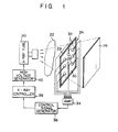
- FIG. 1 is a schematic block circuit diagram of an automatic X-ray exposure control apparatus provided with a semiconductor radiation sensor arrangement according to one embodiment of this invention.
- X-rays emitted from an X-ray tube 20 pass through an object 22, are detected by an X-ray detecting apparatus 24, and impinge on a direct radiography film 26 (hereinafter simply referred to as "an X-ray film") to form a radiographic image of an object thereon.
- the X-ray film 26 is received in a cassette together with an X-ray intensifying screen.
- the cassette is supported by a cassette holder. (Neither X-ray intensifying screen nor cassette is indicated.)
- the X-ray detecting apparatus 24 includes a plurality of ring-shaped semiconductor radiation sensors 28 fixed in holes penetrating mounts, respectively.
- the mounts are, respectively, securely engaged with holes penetrating a substrate 30 which is rigidly supported at the marginal portions by a frame 29.
- the X-ray detecting apparatus 24 detects an X-ray dosage to convert it into an electric signal which in turn is couple through leads 32 to an amplifier 34.
- the electric signal is amplified by the amplifier 34., and thereafter supplied to a control signal generator 36.
- the control signal generator 36 includes an integrator which integrates the output signal of the amplifier 34 with respect to time and a comparator which compares the output of the integrator with a reference signal indicative of an optimum X-ray exposure condition, and provides an X-ray controller 38 with an X-ray shutting signal when the output level of the integrator reaches that of the reference signal.
- the optimum X-ray exposure condition is determined to properly impress a radiographic image of an object 22 on the X-ray film 26.
- the X-ray controller 38 stops voltage supply to a high voltage generator 40.
- a plurality of semiconductor radiation sensors 28 may be disposed on any required measuring fields in the positions substantially corresponding to, for example, the breast, head, backbone and abdomen of the human body of which an X-ray photograph (radiograph) is taken.
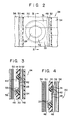
- Figs. 2 and 3 indicate in enlargement part of an X-ray detecting apparatus 24 according to one embodiment of this invention.
- Fig. 3 is a sectional view of said X-ray detecting apparatus 24 on line III-III of Fig. 2.
- the ring-shaped semiconductor radiation sensor 28 has an inner diameter of 25 mm and has its thickness of 300 microns to prevent its shadow from being impressed on an X-ray film.
- the semiconductor radiation sensor 28 as disclosed in the West German Offenlegungsschrift 2,806,858 is formed of an N type high purity silicon single crystal, in which the impurity concentration is z 2x10 12 cm -3 ; the resistivity is x 2.5 k ⁇ cm; a hole life ⁇ ⁇ is z 400 microseconds; and a hole diffusion length Lp is z 0.72 mm. Since the hole diffusion length Lp is z 0.72, the semiconductor radiation sensor 28 can be operated without being impressed with voltage. The semiconductor radiation sensor 28 made thinner than the hole diffusion length L p is little likely to interact with radiation, and indicates an extremely small sensitivity decline even when damaged by radiation.
- the semiconductor radiation sensor 28 is fixed to the surface of a ring-shaped mount 42 which is made from acrylic resin, for example, polymethyl methacrylate with an outer diameter of 40 mm and inner diameter of 25 mm. Both front and back sides of the semiconductor radiation sensor 28 are coated with an aluminum electrode layer (not shown).
- the mount 42 is securely engaged with a hole penetrating the substrate 30 made from, for example, the same polymethyl methacrylate or carbon fiber reinforced plastics (CFRP). Leads 31 and 33 connected to the electrodes of the semiconductor radiation sensor 28 extend along the substrate 30.
- the polymethyl methacrylate which little absorbs X-rays is favorably accepted.
- the semiconductor radiation sensor 28 should preferably be made as thin as 100 to 800 microns of aluminum equivalent thickness in order to reduce its absorption of X-rays at anode voltage 50 to 150 kV of the X-ray tube 20 and prevent its shadow from being impressed on an X-ray film.
- the leads 31 and 33 be formed of an aluminum layer having a smaller thickness than 80 microns.
- the semiconductor radiation sensor 28, mount 42, substrate 30 and leads 31 and 33 are made from a specified material with a prescribed thickness.
- the outer portion 41 of the peripheral wall of the mount 42 (namely, that portion of the mount 42 which is engaged with the substrate 30), and the inner portion 43 of the peripheral wall of the mount 42 jointly define a tapered form.
- the mount 42 thus constructed suppresses the ununiform attenuation of X-rays in the boundary between the mount 42 and the substrate 30, and the boundary between the mount 42 and the semiconductor radiation sensor 28. Therefore, the shadows of the boundaries are prevented from being impressed on an X-ray film, thereby ensuring a distinct image.
- Thin insulation layers 46 and 48 formed of, for example, mica are provided in parallel with both sides of the substrate 30. Further, electromagnetic shielding members 50 and 52 made of, for example, aluminum foil are respectively mounted on the insulation layers 46 and 48, thereby preventing an electric signal generated by the semiconductor radiation sensor 28 from being - disturbed by noises.
- a cover 54 made from, for example, polyester film is mounted on the aluminum foil 52 to protect the semiconductor radiation sensor 28 and also to render the X-ray detecting apparatus 24 attractive.
- a grid 56 which is made of, for example, lead (Pb) to eliminate scattered X-rays and has a-thickness of 3 mm is mounted on the aluminum foil 50 provided on that side of the X-ray detecting apparatus 24 on which X-rays are introduced.
- the grid 56 is put, proper selection is made of the material filled in a space defined between every two adjacent parallel arranged grid components (for example, aluminum or wood); the grid ratio (for example, 8:1 or 10:1); the number of the grid components (for example 34 lp/cm, or 40 zpjcm, wherein Zp denotes a line pair); and a distance from the X-ray focus (for example, 80 cm or 100 cm).
- the grid ratio for example, 8:1 or 10:1
- the number of the grid components for example 34 lp/cm, or 40 zpjcm, wherein Zp denotes a line pair
- Zp denotes a line pair
- a distance from the X-ray focus for example, 80 cm or 100 cm.
- the mechanically strong grid 56 is used as one of the components of the X-ray detecting apparatus 24, making it possible to use a thin substrate 30.
- the grid 56 concurrently acts as a protective member for the X-ray detecting apparatus 24, making it unnecessary to provide any protective layer such as the cover 54 on that side of the X-ray detecting apparatus 24 on which the grid 56 is set. Therefore, a typical configuration of X-ray detecting apparatus 24 can be - chosen to have a thickness of about 6 mm, thereby reducing a distance between the object 22 and the X-ray film 26 and consequently the rate at which X-rays are geometrically magnified.
- the material of the substrate 30 can be selected over a wide range of mechanical strength, allowing for the easy design of the X-ray detecting apparatus 24.
- Fig. 4 Description is now given with reference to Fig. 4 of an X-ray detecting apparatus 60 according to another embodiment of this invention.
- two grids are generally provided between the object 22 and the X-ray film 26 (see Fig. 1), in such a mahner that the parallel arranged components of one of the paired grids intersect those of the other grid at right angles.
- the paired grids are hereinafter referred to as "crosswise intersecting grids".
- two grids 56 and 58 (Fig. 4) are integrally assembled characteristically of this invention with the semiconductor radiation sensors 28 to constitute the X-ray detecting apparatus 60.
- the cover 54 of the X-ray detecting apparatus 24 of Fig. 2 is replaced by the second grid 58 crosswise intersecting the first grid 56.
- the crosswise intersecting grids 56 and 58 not only more effectively eliminate scattered X-rays but also make a distance between an object 22 and X-ray film 26 shorter than the conventional arrangement in which the two grids 56 and 58 and semiconductor radiation sensors 28 are separately provided.
- the first and second grids 56 and 58 should preferably be positioned on both sides of the substrate 30 in crosswise intersecting relationship. However, it is possible to provide both crosswise intersecting grids 56 and 58 on one side of the substrate 30 in a mutually superposed state. In the latter case, it is advised to provide a cover on that side of the substrate 30 on which said grids 56 and 58 are not provided.
Landscapes
- Health & Medical Sciences (AREA)
- Spectroscopy & Molecular Physics (AREA)
- Life Sciences & Earth Sciences (AREA)
- General Physics & Mathematics (AREA)
- High Energy & Nuclear Physics (AREA)
- Molecular Biology (AREA)
- Physics & Mathematics (AREA)
- General Health & Medical Sciences (AREA)
- Toxicology (AREA)
- Measurement Of Radiation (AREA)
- X-Ray Techniques (AREA)
- Apparatus For Radiation Diagnosis (AREA)
- Light Receiving Elements (AREA)
Applications Claiming Priority (2)
| Application Number | Priority Date | Filing Date | Title |
|---|---|---|---|
| JP23706/80 | 1980-02-27 | ||
| JP2370680A JPS56119876A (en) | 1980-02-27 | 1980-02-27 | Semiconductor x-ray detector |
Publications (3)
| Publication Number | Publication Date |
|---|---|
| EP0035182A2 true EP0035182A2 (fr) | 1981-09-09 |
| EP0035182A3 EP0035182A3 (en) | 1983-01-26 |
| EP0035182B1 EP0035182B1 (fr) | 1985-11-21 |
Family
ID=12117794
Family Applications (1)
| Application Number | Title | Priority Date | Filing Date |
|---|---|---|---|
| EP81101195A Expired EP0035182B1 (fr) | 1980-02-27 | 1981-02-19 | Assemblage de détecteurs de rayonnement à semi-conducteur pour un dispositif de commande automatique du temps de pose d'une radiographie |
Country Status (6)
| Country | Link |
|---|---|
| US (1) | US4403150A (fr) |
| EP (1) | EP0035182B1 (fr) |
| JP (1) | JPS56119876A (fr) |
| AU (1) | AU528620B2 (fr) |
| BR (1) | BR8101191A (fr) |
| DE (1) | DE3172939D1 (fr) |
Cited By (4)
| Publication number | Priority date | Publication date | Assignee | Title |
|---|---|---|---|---|
| DE3242067A1 (de) * | 1982-11-13 | 1984-05-17 | Koch & Sterzel Gmbh & Co, 4300 Essen | Roentgenstrahlenmesskammer mit siliziumhalbleiterdetektoren |
| FR2594288A1 (fr) * | 1986-02-11 | 1987-08-14 | Radiante Oy | Procede pour photographier un objet au moyen d'un appareil panoramique a rayons x muni d'un dispositif d'exposition automatique |
| FR2732473A1 (fr) * | 1995-03-31 | 1996-10-04 | Sagem | Dosimetre a eclairage par l'arriere |
| EP0779521A1 (fr) * | 1995-12-14 | 1997-06-18 | General Electric Company | Détecteur de rayons X pour le contrÔle automatique de l'exposition dans un appareil d'imagerie |
Families Citing this family (8)
| Publication number | Priority date | Publication date | Assignee | Title |
|---|---|---|---|---|
| JPS5945A (ja) * | 1982-06-22 | 1984-01-05 | 株式会社東芝 | X線撮影装置 |
| JPS60119100A (ja) * | 1983-11-30 | 1985-06-26 | Toshiba Corp | X線装置 |
| DE8621546U1 (de) * | 1986-08-11 | 1987-12-10 | Siemens AG, 1000 Berlin und 8000 München | Röntgendetektorsystem |
| US5066861A (en) * | 1987-07-22 | 1991-11-19 | Kanegafuchi Chemical Industry Co., Ltd. | X ray detecting device |
| US5264328A (en) * | 1992-04-24 | 1993-11-23 | International Business Machines Corporation | Resist development endpoint detection for X-ray lithography |
| DE4446865C2 (de) * | 1994-12-27 | 2001-06-21 | Siemens Ag | Mammographie-Röntgengerät |
| DE19811556A1 (de) * | 1998-03-17 | 1999-09-23 | Philips Patentverwaltung | Strahlungsmeßeinrichtung mit einer Ionisatonskammer |
| JP5629445B2 (ja) * | 2009-09-25 | 2014-11-19 | キヤノン株式会社 | X線画像撮影装置 |
Family Cites Families (8)
| Publication number | Priority date | Publication date | Assignee | Title |
|---|---|---|---|---|
| US2747104A (en) * | 1951-10-06 | 1956-05-22 | Gen Electric | Interval timing apparatus |
| US2824970A (en) * | 1952-04-04 | 1958-02-25 | Ledin Sven Harald | Secondary diaphragms for x-ray radiography |
| US3255351A (en) * | 1963-04-19 | 1966-06-07 | Nuclear Diodes Inc | Particle detector of the semiconductor type |
| US4039841A (en) * | 1976-02-11 | 1977-08-02 | Spectronics Corporation | X-ray grid adaptor |
| US4082957A (en) * | 1976-04-29 | 1978-04-04 | Morlan Alva F | X-ray absorbing wedge for improving soft tissue outline |
| GB1559664A (en) * | 1977-02-17 | 1980-01-23 | Tokyo Shibaura Electric Co | Semiconductor radiation detector |
| JPS5574480A (en) * | 1978-11-30 | 1980-06-05 | Toshiba Corp | Semiconductor x-ray detector for use in x-ray exposure control device |
| US4288264A (en) * | 1979-11-21 | 1981-09-08 | Emi Limited | Detector construction |
-
1980
- 1980-02-27 JP JP2370680A patent/JPS56119876A/ja active Granted
-
1981
- 1981-02-18 US US06/236,133 patent/US4403150A/en not_active Expired - Fee Related
- 1981-02-19 DE DE8181101195T patent/DE3172939D1/de not_active Expired
- 1981-02-19 EP EP81101195A patent/EP0035182B1/fr not_active Expired
- 1981-02-19 AU AU67465/81A patent/AU528620B2/en not_active Ceased
- 1981-02-26 BR BR8101191A patent/BR8101191A/pt unknown
Cited By (5)
| Publication number | Priority date | Publication date | Assignee | Title |
|---|---|---|---|---|
| DE3242067A1 (de) * | 1982-11-13 | 1984-05-17 | Koch & Sterzel Gmbh & Co, 4300 Essen | Roentgenstrahlenmesskammer mit siliziumhalbleiterdetektoren |
| EP0111172A1 (fr) * | 1982-11-13 | 1984-06-20 | General Electric-Cgr Gmbh Und Co Kg | Détecteur en silicium pour rayons X |
| FR2594288A1 (fr) * | 1986-02-11 | 1987-08-14 | Radiante Oy | Procede pour photographier un objet au moyen d'un appareil panoramique a rayons x muni d'un dispositif d'exposition automatique |
| FR2732473A1 (fr) * | 1995-03-31 | 1996-10-04 | Sagem | Dosimetre a eclairage par l'arriere |
| EP0779521A1 (fr) * | 1995-12-14 | 1997-06-18 | General Electric Company | Détecteur de rayons X pour le contrÔle automatique de l'exposition dans un appareil d'imagerie |
Also Published As
| Publication number | Publication date |
|---|---|
| AU6746581A (en) | 1982-12-23 |
| EP0035182A3 (en) | 1983-01-26 |
| US4403150A (en) | 1983-09-06 |
| JPS645268B2 (fr) | 1989-01-30 |
| BR8101191A (pt) | 1981-09-01 |
| EP0035182B1 (fr) | 1985-11-21 |
| JPS56119876A (en) | 1981-09-19 |
| DE3172939D1 (en) | 1986-01-02 |
| AU528620B2 (en) | 1983-05-05 |
Similar Documents
| Publication | Publication Date | Title |
|---|---|---|
| Boyer et al. | A review of electronic portal imaging devices (EPIDs) | |
| US5585638A (en) | X-ray detector for automatic exposure control of an imaging apparatus | |
| US6316773B1 (en) | Multi-density and multi-atomic number detector media with gas electron multiplier for imaging applications | |
| CA2309097C (fr) | Procede et dispositif de radiographie a faisceau plan et detecteur de rayonnement | |
| US4831260A (en) | Beam equalization method and apparatus for a kinestatic charge detector | |
| EP0488991B1 (fr) | Procédé de production d'images fluoroscopiques et radiographiques à rayons x et appareil diagnostique portatif fonctionnant d'après ce procédé | |
| US4403150A (en) | Semiconductor radiation sensor arrangement for an automatic X-ray exposure control apparatus | |
| KR100682080B1 (ko) | 방사사진술을 위한 방법 및 장치와 방사검출기 | |
| EP0403135A2 (fr) | Détecteur de rayons X | |
| CA2419869A1 (fr) | Milieux de detection de densites et nombres atomiques multiples avec multiplicateur d'electron de gaz pour des applications en imagerie | |
| JP2769558B2 (ja) | 画像均等化付スリット放射線写真用装置 | |
| JPH06100657B2 (ja) | X線写真装置 | |
| US6236711B1 (en) | Radiation measuring device comprising an ionization chamber | |
| EP0365353B1 (fr) | Système de radiographie à balayage et détecteur d'égalisation pour un tel système | |
| CA2200923C (fr) | Methode d'imagerie en megavolts combinant un photorecepteur et un convertisseur et concentrateur de photons a haute energie | |
| WO2000055866A1 (fr) | Source de rayons gamma pour la radiographie | |
| US4795909A (en) | High performance front window for a kinestatic charge detector | |
| JPH06160535A (ja) | 放射線検出器 | |
| EP0426842A1 (fr) | Imagerie quantitative employant la radiographie a egalisation du balayage | |
| JP2000133491A (ja) | X線ホトタイマ検出器 | |
| JPS6345072B2 (fr) | ||
| JP3643459B2 (ja) | 自動露出制御装置用x線検出器 | |
| Sones et al. | Measured performance characteristics of a solid‐state linear detector array | |
| Bednarek et al. | Comparison of two dose-area-product ionization chambers with different conductive surface coating for over-table and under-table tube configurations | |
| JPS58223145A (ja) | X線診断装置用カセツテ |
Legal Events
| Date | Code | Title | Description |
|---|---|---|---|
| PUAI | Public reference made under article 153(3) epc to a published international application that has entered the european phase |
Free format text: ORIGINAL CODE: 0009012 |
|
| 17P | Request for examination filed |
Effective date: 19810219 |
|
| AK | Designated contracting states |
Designated state(s): DE FR GB NL |
|
| PUAL | Search report despatched |
Free format text: ORIGINAL CODE: 0009013 |
|
| AK | Designated contracting states |
Designated state(s): DE FR GB NL |
|
| RAP1 | Party data changed (applicant data changed or rights of an application transferred) |
Owner name: KABUSHIKI KAISHA TOSHIBA |
|
| GRAA | (expected) grant |
Free format text: ORIGINAL CODE: 0009210 |
|
| AK | Designated contracting states |
Designated state(s): DE FR GB NL |
|
| REF | Corresponds to: |
Ref document number: 3172939 Country of ref document: DE Date of ref document: 19860102 |
|
| ET | Fr: translation filed | ||
| PLBE | No opposition filed within time limit |
Free format text: ORIGINAL CODE: 0009261 |
|
| STAA | Information on the status of an ep patent application or granted ep patent |
Free format text: STATUS: NO OPPOSITION FILED WITHIN TIME LIMIT |
|
| 26N | No opposition filed | ||
| PGFP | Annual fee paid to national office [announced via postgrant information from national office to epo] |
Ref country code: GB Payment date: 19910212 Year of fee payment: 11 Ref country code: FR Payment date: 19910212 Year of fee payment: 11 |
|
| PGFP | Annual fee paid to national office [announced via postgrant information from national office to epo] |
Ref country code: NL Payment date: 19910228 Year of fee payment: 11 |
|
| PGFP | Annual fee paid to national office [announced via postgrant information from national office to epo] |
Ref country code: DE Payment date: 19910328 Year of fee payment: 11 |
|
| PG25 | Lapsed in a contracting state [announced via postgrant information from national office to epo] |
Ref country code: GB Effective date: 19920219 |
|
| PG25 | Lapsed in a contracting state [announced via postgrant information from national office to epo] |
Ref country code: NL Effective date: 19920901 |
|
| GBPC | Gb: european patent ceased through non-payment of renewal fee | ||
| NLV4 | Nl: lapsed or anulled due to non-payment of the annual fee | ||
| PG25 | Lapsed in a contracting state [announced via postgrant information from national office to epo] |
Ref country code: FR Effective date: 19921030 |
|
| PG25 | Lapsed in a contracting state [announced via postgrant information from national office to epo] |
Ref country code: DE Effective date: 19921103 |
|
| REG | Reference to a national code |
Ref country code: FR Ref legal event code: ST |