EP0036157B1 - Nieder-Temperatur-Glühen von Halbleitervorrichtungen - Google Patents
Nieder-Temperatur-Glühen von Halbleitervorrichtungen Download PDFInfo
- Publication number
- EP0036157B1 EP0036157B1 EP81101689A EP81101689A EP0036157B1 EP 0036157 B1 EP0036157 B1 EP 0036157B1 EP 81101689 A EP81101689 A EP 81101689A EP 81101689 A EP81101689 A EP 81101689A EP 0036157 B1 EP0036157 B1 EP 0036157B1
- Authority
- EP
- European Patent Office
- Prior art keywords
- semiconductor
- lattice
- ion implanted
- annealing
- radiation
- Prior art date
- Legal status (The legal status is an assumption and is not a legal conclusion. Google has not performed a legal analysis and makes no representation as to the accuracy of the status listed.)
- Expired
Links
Images
Classifications
-
- H—ELECTRICITY
- H10—SEMICONDUCTOR DEVICES; ELECTRIC SOLID-STATE DEVICES NOT OTHERWISE PROVIDED FOR
- H10P—GENERIC PROCESSES OR APPARATUS FOR THE MANUFACTURE OR TREATMENT OF DEVICES COVERED BY CLASS H10
- H10P95/00—Generic processes or apparatus for manufacture or treatments not covered by the other groups of this subclass
- H10P95/90—Thermal treatments, e.g. annealing or sintering
Definitions
- the invention relates to the annealing of semiconductor devices, and in particular the healing of radiation damage to semiconductor crystals that occurs during implantation of impurities.
- Another technique to promote localized annealing is to place the wafer in a high temperature (800-1100°C) furnace. Such high temperature processing however causes degradation in the overall yield and performance of the semiconductor devices. Prior to the present invention there has not been a suitable low temperature annealing technique for healing the radiation damage to semiconductor crystals.
- US-A-4,013,485 relates to a process of eliminating undesirable charge centers in MIS devices by the use of a RF field. While this citation mentions experiments which indicated that frequencies in the microwave range can have a beneficial effect in repairing radiation damage, it fails to recognize that in one fabrication step of a process for fabricating a semiconductor device, the device comprising a semiconductor substrate having a major surface including an ion implanted region subsequent to the formation of the ion implanted regions a low temperature annealing effect is obtained by directing a beam of microwave radiation in the range of 1 to 10 gHz at said entire device so that the electromagnetic field of the microwave radiation couples with the semiconductor lattice of the ion implanted region causing lattice heating due to the release of photons, the remaining non-implanted silicon being essentially transparent to the radiation.
- the present invention provides a process for fabricating a semi- conducor device as set forth in claim 1.
- Preferred embodiments of the invention are claimed in the dependent claims.
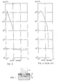
- FIG. 1 there is shown a highly simplified diagrammatic view of the process according to the present invention.
- a substrate material 10 which in a preferred embodiment is a semiconductor such as silicon or gallium arsenide, or other substrates susceptible to advantageous ion implant processes, is provided.
- the substrate is covered, but for the window shown, by a masking layer 11, such as silicon dioxide.
- An electromagnetic wave having a frequency in the microwave portion of the spectrium is indicated by the schematic beam 13 and is incident on the window.
- Reference numeral 12 indicates the position of the impurity boundary after ion implanting of the region under the window and before annealing.
- the semiconductor region anneals.
- the annealing process can be adopted and controlled either to minimize redistribution or to achieve a controlled movement of implanted impurities.
- the present invention is based upon the fact that the energy of electromagnetic radiation can be coupled to a crystalline lattice, or even to a damaged crystalline lattice.
- the coupling of such energy to an ionized impurity in the lattice increases the local temperature of the lattice, so that the impurity atom and the surrounding lattice .structure seeks the lowest free energy configuration which would still be an ordered crystal structure.
- the increase in the local temperature of the lattice could be due to the coupling of the electromagnetic radiation with a local oscillator formed by the molecular configuration including the impurity.
- Lattice heating is also associated with the release of phonons.
- the method according to the present invention couples the energy from the microwave radiation to the implanted dopant species and the damaged semiconductor crystal.
- the energy would typically be dissipated as phonons in the lattice, causing mechanical vibration and heat to be generated.
- the ionized impurities become substitutional in the lattice, eddy currents in the doped regions will also be induced resulting in increased heating which may aid in the annealing.
- One application of the present invention is to promote localized annealing in integrated circuits at a low temperature.
- localized annealing is primarily done in a high temperature (800-1100°) furnace. High temperature steps cause degradation in overall yield and performance.
- the search for a low temperature annealing technique has been underway since the discovery of laser annealing, see, for example B. A. Kachu- rin, N. B. Pridachin and L. S. Smirnov, Sov. Phys. - Semicond. 9, 946 (1975).
- the absorption spectrum of the local defect size created by the ion implanted specie has a broad frequency range. It is expected that one can couple the lower frequency radiation with sufficient power to cause annealing.
- FIG. 2 is the concentration profile obtained on one half of the test wafer that was thermally annealed according to techniques known in the prior art.
- the anneal conditions were 1000°C, 30 mins in N 2 .
- the figure indicates that although complete electrical activation of the implanted specie has been obtained, the impurity has redistributed within the sample to increase the junction depth from approximately 0.5 um in the 'as-implanted' wafers to 0.8 um in the thermally annealed samples.
- FIG. 3 is the concentration profile on one half of a test wafer obtained after the same test wafer was annealed for 30 mins. in a commercial microwave oven according to the present invention.
- the ambient was a partial vacuum which was obtained by enclosing the sample in a quartz capsule.
- the implant specie was phosphorus with a concentration of 5 x 10 14 /cm 2 implanted at 100 KeV.
- the substrate material was p-type silicon.
- the profile in FIG. 3 was obtained from a spreading resistance measurement performed on a beveled surface. It can be seen from this figure that only partial activation was achieved in this duration of 30 mins. and that there was no appreciable impurity distribution.
- the semiconductor device according to the present invention can be manufactured with various semiconductor technologies and different combinations of known process steps, and that the preferred embodiments illustrated here are merely exemplary.
- the depth of penetration of the various zones and regions and in particular the configuration and distance between the active zones of the transistor devices, as well as the concentrations of dopant species, and/or their concentration profiles, can be chosen depending upon the desired properties.
- the present invention is also not restricted to the specific semiconductor materials and circuits described.
- semiconductor materials other than silicon for example AIII-Bv compounds
- the conductivity types in the embodiment may be interchanged and corresponding to such change, the polarity of the respective operating voltages adapted.
- the voltage level and the static or dynamic nature of the signals applied to the various terminals and gates of the device, as well as the voltage sources, may be suitably selected as desired for a particular application.
Landscapes
- Recrystallisation Techniques (AREA)
- Insulated Gate Type Field-Effect Transistor (AREA)
Claims (4)
Applications Claiming Priority (2)
| Application Number | Priority Date | Filing Date | Title |
|---|---|---|---|
| US130509 | 1980-03-14 | ||
| US06/130,509 US4303455A (en) | 1980-03-14 | 1980-03-14 | Low temperature microwave annealing of semiconductor devices |
Publications (2)
| Publication Number | Publication Date |
|---|---|
| EP0036157A1 EP0036157A1 (de) | 1981-09-23 |
| EP0036157B1 true EP0036157B1 (de) | 1985-08-28 |
Family
ID=22445017
Family Applications (1)
| Application Number | Title | Priority Date | Filing Date |
|---|---|---|---|
| EP81101689A Expired EP0036157B1 (de) | 1980-03-14 | 1981-03-09 | Nieder-Temperatur-Glühen von Halbleitervorrichtungen |
Country Status (4)
| Country | Link |
|---|---|
| US (1) | US4303455A (de) |
| EP (1) | EP0036157B1 (de) |
| JP (1) | JPS56144545A (de) |
| DE (1) | DE3171974D1 (de) |
Cited By (1)
| Publication number | Priority date | Publication date | Assignee | Title |
|---|---|---|---|---|
| DE10229642A1 (de) * | 2002-07-02 | 2004-01-29 | Infineon Technologies Ag | Verfahren zum lokalen Erhitzen eines in einem Halbleitersubstrat angeordneten Bereichs |
Families Citing this family (33)
| Publication number | Priority date | Publication date | Assignee | Title |
|---|---|---|---|---|
| US4372990A (en) * | 1980-06-23 | 1983-02-08 | Texas Instruments Incorporated | Retaining wall technique to maintain physical shape of material during transient radiation annealing |
| GB2106709B (en) * | 1981-09-17 | 1986-11-12 | Itt Ind Ltd | Semiconductor processing |
| FR2513659A1 (fr) * | 1981-09-29 | 1983-04-01 | Centre Nat Rech Scient | Procede de recuit superficiel par energie micro-onde pulsee de materiaux semi-conducteurs |
| JPS5891621A (ja) * | 1981-11-26 | 1983-05-31 | Mitsubishi Electric Corp | 半導体装置の製造方法 |
| JPS58177469A (ja) * | 1982-04-09 | 1983-10-18 | Fujitsu Ltd | 半導体基板の加熱方法及び加熱装置 |
| JPH0669027B2 (ja) * | 1983-02-21 | 1994-08-31 | 株式会社日立製作所 | 半導体ウエハの薄膜形成方法 |
| GB2179496B (en) * | 1985-08-23 | 1989-08-09 | Marconi Electronic Devices | A method of controlling a distribution of carrier lifetimes within a semiconductor material |
| FR2670950B1 (fr) * | 1990-12-20 | 1993-04-16 | Motorola Semiconducteurs | Procede et appareil pour le traitement de recuit des dispositifs a semiconducteur. |
| US5519193A (en) * | 1992-10-27 | 1996-05-21 | International Business Machines Corporation | Method and apparatus for stressing, burning in and reducing leakage current of electronic devices using microwave radiation |
| US6051483A (en) * | 1996-11-12 | 2000-04-18 | International Business Machines Corporation | Formation of ultra-shallow semiconductor junction using microwave annealing |
| KR100297498B1 (ko) * | 1996-11-20 | 2001-10-24 | 윤덕용 | 마이크로파를이용한다결정박막의제조방법 |
| US6051283A (en) * | 1998-01-13 | 2000-04-18 | International Business Machines Corp. | Microwave annealing |
| JPH11295383A (ja) * | 1998-04-15 | 1999-10-29 | Mitsubishi Electric Corp | マイクロ波帯域用半導体トランジスタのバーンイン方法、バーンイン装置及びバーンインした半導体装置 |
| TW449931B (en) | 2000-01-27 | 2001-08-11 | United Epitaxy Co Ltd | Manufacturing method of P-type semiconductor with a low resistance coefficient |
| EP1130659A1 (de) * | 2000-03-03 | 2001-09-05 | United Epitaxy Company, Ltd. | Verfahren zur Herstellung von p-Typ-Verbindungshalbleitermaterial mit niedrigem spezifischem Widerstand |
| TW541628B (en) * | 2001-06-04 | 2003-07-11 | Matsushita Electric Industrial Co Ltd | Annealing method and method and device for forming ultra-shallow junction layer |
| JP4090225B2 (ja) * | 2001-08-29 | 2008-05-28 | 東京エレクトロン株式会社 | 半導体装置の製造方法、及び、基板処理方法 |
| US7026229B2 (en) * | 2001-11-28 | 2006-04-11 | Vartan Semiconductor Equipment Associates, Inc. | Athermal annealing with rapid thermal annealing system and method |
| US6884328B2 (en) * | 2001-11-29 | 2005-04-26 | Seagate Technology Llc | Selective annealing of magnetic recording films |
| US20030186519A1 (en) * | 2002-04-01 | 2003-10-02 | Downey Daniel F. | Dopant diffusion and activation control with athermal annealing |
| US7176112B2 (en) * | 2004-09-21 | 2007-02-13 | Atmel Corporation | Non-thermal annealing with electromagnetic radiation in the terahertz range of doped semiconductor material |
| US7985617B2 (en) * | 2008-09-11 | 2011-07-26 | Micron Technology, Inc. | Methods utilizing microwave radiation during formation of semiconductor constructions |
| TWI384556B (zh) * | 2008-11-12 | 2013-02-01 | 財團法人國家實驗研究院 | Microwave activation annealing process |
| JP2011077065A (ja) * | 2009-09-29 | 2011-04-14 | Tokyo Electron Ltd | 熱処理装置 |
| US20130023111A1 (en) * | 2011-06-29 | 2013-01-24 | Purtell Robert J | Low temperature methods and apparatus for microwave crystal regrowth |
| US20130023097A1 (en) * | 2011-07-14 | 2013-01-24 | Purtell Robert J | U-mos trench profile optimization and etch damage removal using microwaves |
| US20140094023A1 (en) * | 2012-09-28 | 2014-04-03 | National Applied Research Laboratories | Fabricating method of semiconductor chip |
| CN105390382A (zh) * | 2015-10-22 | 2016-03-09 | 中国科学院微电子研究所 | 一种iii族氮化物电子器件低温欧姆接触的制作方法 |
| CN114823307B (zh) * | 2022-06-15 | 2025-04-15 | 季华实验室 | 一种半导体退火方法、退火装置及退火系统 |
| KR102837636B1 (ko) | 2024-03-22 | 2025-07-23 | (주)울텍 | 마이크로파 열처리 장치 |
| KR102933660B1 (ko) | 2024-04-26 | 2026-03-05 | (주)울텍 | 유전체 물질을 이용한 마이크로파 열처리 장치 |
| KR102942984B1 (ko) | 2024-06-20 | 2026-03-25 | (주)울텍 | 가열 위치 조절이 가능한 마이크로파 열처리 장치 |
| KR102924591B1 (ko) | 2025-04-17 | 2026-02-09 | (주)울텍 | 균일 가열을 위한 마이크로파 열처리 장치 |
Citations (2)
| Publication number | Priority date | Publication date | Assignee | Title |
|---|---|---|---|---|
| US4013485A (en) * | 1976-04-29 | 1977-03-22 | International Business Machines Corporation | Process for eliminating undesirable charge centers in MIS devices |
| DE2705444A1 (de) * | 1977-02-09 | 1978-08-10 | Siemens Ag | Verfahren zur lokal begrenzten erwaermung eines festkoerpers |
Family Cites Families (7)
| Publication number | Priority date | Publication date | Assignee | Title |
|---|---|---|---|---|
| US3777099A (en) * | 1968-02-09 | 1973-12-04 | M Levinson | Methods of heating an article in a microwave oven |
| JPS4825816A (de) * | 1971-08-11 | 1973-04-04 | ||
| JPS5823349B2 (ja) * | 1975-08-11 | 1983-05-14 | 新日本製鐵株式会社 | タイカブツノシヨウケツホウホウ |
| FR2371226A1 (fr) * | 1976-11-17 | 1978-06-16 | Olivier Jean | Applicateur pour soumettre une matiere a des ondes |
| IT1078456B (it) * | 1977-06-03 | 1985-05-08 | Vitali Gian Franco | Perfezionamento nei procedimenti per la produzione di dispositivi a semiconduttore |
| US4240843A (en) * | 1978-05-23 | 1980-12-23 | Western Electric Company, Inc. | Forming self-guarded p-n junctions by epitaxial regrowth of amorphous regions using selective radiation annealing |
| US4181538A (en) * | 1978-09-26 | 1980-01-01 | The United States Of America As Represented By The United States Department Of Energy | Method for making defect-free zone by laser-annealing of doped silicon |
-
1980
- 1980-03-14 US US06/130,509 patent/US4303455A/en not_active Expired - Lifetime
-
1981
- 1981-03-09 DE DE8181101689T patent/DE3171974D1/de not_active Expired
- 1981-03-09 EP EP81101689A patent/EP0036157B1/de not_active Expired
- 1981-03-10 JP JP3594081A patent/JPS56144545A/ja active Pending
Patent Citations (2)
| Publication number | Priority date | Publication date | Assignee | Title |
|---|---|---|---|---|
| US4013485A (en) * | 1976-04-29 | 1977-03-22 | International Business Machines Corporation | Process for eliminating undesirable charge centers in MIS devices |
| DE2705444A1 (de) * | 1977-02-09 | 1978-08-10 | Siemens Ag | Verfahren zur lokal begrenzten erwaermung eines festkoerpers |
Non-Patent Citations (1)
| Title |
|---|
| Mc GRAW-HILL Encyclopedia, Halbleitertechnologie * |
Cited By (3)
| Publication number | Priority date | Publication date | Assignee | Title |
|---|---|---|---|---|
| DE10229642A1 (de) * | 2002-07-02 | 2004-01-29 | Infineon Technologies Ag | Verfahren zum lokalen Erhitzen eines in einem Halbleitersubstrat angeordneten Bereichs |
| US6900130B2 (en) | 2002-07-02 | 2005-05-31 | Infineon Technologies Ag | Method for locally heating a region in a semiconductor substrate |
| DE10229642B4 (de) * | 2002-07-02 | 2007-03-22 | Infineon Technologies Ag | Verfahren zum lokalen Erhitzen eines in einem Halbleitersubstrat angeordneten vergrabenen Bereichs |
Also Published As
| Publication number | Publication date |
|---|---|
| US4303455A (en) | 1981-12-01 |
| JPS56144545A (en) | 1981-11-10 |
| DE3171974D1 (en) | 1985-10-03 |
| EP0036157A1 (de) | 1981-09-23 |
Similar Documents
| Publication | Publication Date | Title |
|---|---|---|
| US4303455A (en) | Low temperature microwave annealing of semiconductor devices | |
| US5661043A (en) | Forming a buried insulator layer using plasma source ion implantation | |
| US6051483A (en) | Formation of ultra-shallow semiconductor junction using microwave annealing | |
| US4659392A (en) | Selective area double epitaxial process for fabricating silicon-on-insulator structures for use with MOS devices and integrated circuits | |
| US6537886B2 (en) | Ultra-shallow semiconductor junction formation | |
| JP4526819B2 (ja) | キセノン(Xe)による事前非晶質化のためのインプランテーション | |
| JPS60102732A (ja) | シリコンのデンドライトウエブ光電池製造方法 | |
| US4243433A (en) | Forming controlled inset regions by ion implantation and laser bombardment | |
| US6013566A (en) | Method of forming a doped region in a semiconductor substrate | |
| US7026229B2 (en) | Athermal annealing with rapid thermal annealing system and method | |
| EP0958595A1 (de) | Neuer nicht-thermischer temperprozess für kristalline materialien | |
| JP2005522050A (ja) | 非熱的アニーリングを用いたドーパント拡散及び活性化制御 | |
| US5219798A (en) | Method of heating a semiconductor substrate capable of preventing defects in crystal from occurring | |
| Cummings et al. | Rapid annealing of GaAs: Uniformity and temperature dependence of activation | |
| McMahon et al. | Characterisation of multiple-scan electron beam annealing method | |
| US6117749A (en) | Modification of interfacial fields between dielectrics and semiconductors | |
| US6806147B1 (en) | Method and apparatus for suppressing the channeling effect in high energy deep well implantation | |
| EP0803894A1 (de) | Vorrichtungen und Verfahren zur kombinierten Ionenstrahl- und Mikrowellen-Bestrahlung | |
| US6358823B1 (en) | Method of fabricating ion implanted doping layers in semiconductor materials and integrated circuits made therefrom | |
| Razouk et al. | Oxide charges induced in thermal silicon dioxide by scanning electron and laser beam annealing | |
| Kim et al. | Optimizing Collector-Emitter Saturation Voltage at 3000 V Insulated Gate Bipolar Transistors Using Laser Thermal Annealing | |
| KR100250751B1 (ko) | 반도체 소자의 제조방법 | |
| GB2112205A (en) | A thermal processing system for semiconductors and other materials using two or more electron beams | |
| Sheng et al. | Electronically active defects in cw beam‐annealed Si. I. Electron‐beam‐induced current | |
| HK1004085A (en) | Combined ion beam and microwave irradiation means and method |
Legal Events
| Date | Code | Title | Description |
|---|---|---|---|
| PUAI | Public reference made under article 153(3) epc to a published international application that has entered the european phase |
Free format text: ORIGINAL CODE: 0009012 |
|
| AK | Designated contracting states |
Designated state(s): DE FR GB |
|
| 17P | Request for examination filed |
Effective date: 19811030 |
|
| GRAA | (expected) grant |
Free format text: ORIGINAL CODE: 0009210 |
|
| AK | Designated contracting states |
Designated state(s): DE FR GB |
|
| REF | Corresponds to: |
Ref document number: 3171974 Country of ref document: DE Date of ref document: 19851003 |
|
| ET | Fr: translation filed | ||
| PLBE | No opposition filed within time limit |
Free format text: ORIGINAL CODE: 0009261 |
|
| STAA | Information on the status of an ep patent application or granted ep patent |
Free format text: STATUS: NO OPPOSITION FILED WITHIN TIME LIMIT |
|
| 26N | No opposition filed | ||
| PGFP | Annual fee paid to national office [announced via postgrant information from national office to epo] |
Ref country code: FR Payment date: 19980221 Year of fee payment: 18 |
|
| PGFP | Annual fee paid to national office [announced via postgrant information from national office to epo] |
Ref country code: DE Payment date: 19980223 Year of fee payment: 18 |
|
| PGFP | Annual fee paid to national office [announced via postgrant information from national office to epo] |
Ref country code: GB Payment date: 19980226 Year of fee payment: 18 |
|
| PG25 | Lapsed in a contracting state [announced via postgrant information from national office to epo] |
Ref country code: GB Free format text: LAPSE BECAUSE OF NON-PAYMENT OF DUE FEES Effective date: 19990309 |
|
| GBPC | Gb: european patent ceased through non-payment of renewal fee |
Effective date: 19990309 |
|
| PG25 | Lapsed in a contracting state [announced via postgrant information from national office to epo] |
Ref country code: FR Free format text: LAPSE BECAUSE OF NON-PAYMENT OF DUE FEES Effective date: 19991130 |
|
| REG | Reference to a national code |
Ref country code: FR Ref legal event code: ST |
|
| PG25 | Lapsed in a contracting state [announced via postgrant information from national office to epo] |
Ref country code: DE Free format text: LAPSE BECAUSE OF NON-PAYMENT OF DUE FEES Effective date: 20000101 |