EP0037264A2 - Assoziativspeichersystem - Google Patents
Assoziativspeichersystem Download PDFInfo
- Publication number
- EP0037264A2 EP0037264A2 EP81301334A EP81301334A EP0037264A2 EP 0037264 A2 EP0037264 A2 EP 0037264A2 EP 81301334 A EP81301334 A EP 81301334A EP 81301334 A EP81301334 A EP 81301334A EP 0037264 A2 EP0037264 A2 EP 0037264A2
- Authority
- EP
- European Patent Office
- Prior art keywords
- data
- bytes
- read
- tuple
- storing
- Prior art date
- Legal status (The legal status is an assumption and is not a legal conclusion. Google has not performed a legal analysis and makes no representation as to the accuracy of the status listed.)
- Granted
Links
Images


Classifications
-
- G—PHYSICS
- G06—COMPUTING OR CALCULATING; COUNTING
- G06F—ELECTRIC DIGITAL DATA PROCESSING
- G06F16/00—Information retrieval; Database structures therefor; File system structures therefor
- G06F16/90—Details of database functions independent of the retrieved data types
- G06F16/903—Querying
- G06F16/90335—Query processing
- G06F16/90339—Query processing by using parallel associative memories or content-addressable memories
Definitions
- This invention relates to an associative memory system and more particularly, it relates to a method and apparatus for handling data in an associative memory environment.
- Another feature of the improved data base was to access data therefrom by the data itself instead of using an abstract memory location number as a selection device for accessing the data.
- an abstract memory location number For example, a person's social security number itself might be used to provide a means for accessing the data about that person from memory instead of using an abstract or arbitrary location scheme; this provided an apparent associative memory capability.
- U. S. Patent 3448436 describes an associative memory system, wherein a plurality of match circuits are provided. During a search operation, a match circuit is loaded with search information and the contents of an associated track of a disc memory are read into the match circuit. The data on the disc track matching the search information is routed to a display device.
- the problem with such a system is that its use is restricted in that the match circuits can only perform a search operation.
- the match circuits cannot perform operations such as updating or rewriting, which limits the usefulness of the memory system.
- the present invention provides an associative memory system, characterized by storing means for storing data therein, first means and second means for simultaneously receiving at least a portion of a stream of bytes of data as they are read serially from said storing means, said first means including a loop buffer for receiving and storing serially at least a portion of said stream of bytes of data from said storing means, said second means having means for performing at least one operation on at least a portion of said stream of said bytes of data as they are obtained serially from said storing means; and said first means also having means for writing bytes of data from said loop buffer into said storing means simultaneously as said bytes of data are read therefrom, whereby a write address for writing a said byte of data into said storing means is obtained by subtracting a first predetermined number from a current address of a byte of data being read from said storing means.
- the invention provides a method of handling data, characterized by the steps of (a) storing bytes of data in at least first and second blocks of storage elements in a storage array, wherein K bytes of data are obtained serially from said first block followed by K bytes of data obtained serially from said second block, wherein K is a whole number, (b) simultaneously receiving said bytes of data in first and second circuits as they are read from said storage array; said first circuit including a loop buffer for storing serially K bytes of data from said storage array, (c) performing at least one operation on said bytes of data as they are received serially by said second circuit, and (d) writing bytes of data into said storage array via said loop buffer whereby a write address for writing a byte of data into said storage array is obtained by subtracting K from a current address of a byte of data being simultaneously read from said storage array.
- said first means provides a capability of rewriting information into the storing means, thus enabling operations such as updating and rewriting to be carried out.
- data is modified by said second means, written into said loop buffer of said first means and thence into said storing means.
- said storing means includes at least first and second blocks of storage elements, preferably CCD arrays, arranged such that a second predetermined number of bytes of data are obtained serially from said first block followed by a third predetermined number of bytes obtained serially from said second block to provide said stream of bytes of data.
- Said first predetermined number and said second and third predetermined numbers are preferably each equal to K which is a whole number so that, e.g. for CCD arrays having loops of K, data is rewritten to its original location.
- a plurality of associative data controllers may be provided each comprising a said first and a said second means.
- the storing means is divided into a plurality of arrays of blocks of storage elements, each array of blocks being associated with a respective associative data controller so that the data controllers can operate simultaneously on their respective arrays.
- the data in the storage arrays like 310 is stored therein according to the "relational model".
- the relational model may be defined as a mathematically derived methodology for data management which allows solutions to a user's request to be obtained solely through examining the value(s) of the data item(s) in question.
- a simple example would be to use a person's social security number itself (as a means of selection) to obtain personal data from memory about that person instead of using an abstract address to access the personal data.
- the ADC 306 was designed to search through all the data under its control.
- the ADC 306 has the attributes of an associative memory; i.e., given one or more domain values and associated Boolean conditions as qualifiers, the ADC 306 locates all qualifying occurrences of those domain values in the tuples under its control and establishes as one of its functions a "marked" subset of the specified relation as the result.
- a relational model may be considered as a flat table, with the rows of the table being referred to as tuples and the columns thereof being referred to as domains.
- the ADCs such as 306 were also designed to facilitate the searching o,f large amounts of data in parallel.
- the storage arrays like 310 contain CCDs, as previously stated; the arrays can be logically visualized as being a continuous, sequential string of bits with no limiting device characteristics.
- Fig. 2 is a general diagram, in block form, showing how data is stored as relations in the storage arrays (like 310) shown in Fig. 1.
- a relation is divided or split into groups of tuple spaces (occupied and/or deleted) and evenly distributed under all the controllers such as 312, 314 and 318 (Fig. 2), with one group being assigned per controller.
- Each tuple group is allocated a space at the same relative location in the block of storage to which it is assigned.
- a data searching function against a relation can be initiated in parallel by activating all controllers 306, 308 ( F ig. 1) simultaneously, with a request to begin searching (at a particular address) the portion of the relation under their control.
- Fig. 2 illustrates a relation R n which is divided into m tuple groups of equal size, as R 1, R n2 ...R nm .
- FIG. 1 Another attribute of the system 300 (Fig. 1) is that there is a minimum of movement of data within the storage arrays like 310 and a minimum of data being moved from the ADC's like 306 "up" to the PFP 304; i.e., only "answers" are moved up from the ADCs. Another advantage is that a primitive (instruction) from the PFP 304 is processed to completion across all the ADCs instead of dividing the ADCs into subgroups to process multiple primitives against different relations, concurrently.
- the access control unit 302 is essentially a non-hardware, sequential processor of relational data subrequests. The control unit 302 works on a subrequest to completion before accepting a second subrequest.
- All the data required to complete a subrequest is known to be available in the storage arrays like 310.
- the appropriate sequence of hardware primitives is constructed in the control unit 302 and those primitives are sent to the PFP 304, one at a time, in order to be dispersed to the ADCs like 306 and 308 for execution. Only the "answers", if any, are returned to the control unit 302.
- Each ADC such as 306 shown in Fig. 1, is comprised of the modules shown in Fig. 3; these separate modules are designed to process in parallel, the specified data retrieved from the associated storage array 31 0.
- ADC 306 includes a minimum/maximum (min/max) module 3 2 0, a qualify module 322, a tag module 324, read/write module 326, and loop control module 328; a first bus 330 connects each of these modules with the storage array 310, and a second bus 332 is used for presenting data to these modules from a main bus 334.
- the main bus 334 couples the ADC 306 to the PFP 304 via a data interchange unit 336.
- a control logic module 548 is connected to each of the modules in Fig. 3 by a bus 549.
- the basic function of the min/max module 320 (Fig. 3) is to find the minimum or the maximum value of a domain within a single pass of a relation, i.e., in one cycle, the minimum or the maximum value of one domain in a qualified set of tuples will have been found.
- the general function of the qualify module 322 (Fig. 3) is to compare domains from the storage array 310 with the argument data sent over the bus 334 to determine whether or not a current tuple is the one which is to be selected according to conditions set up for selection at the PFP 304.
- the general function of the tag module 324 (Fig. 3) is to mark or tag certain data which is selected in one operation for use in a subsequent operation.
- the general function of the tag module 324 is to mark or tag certain data which is selected in one operation for use in a subsequent operation.
- select data by content in the associative method of retrieval there is no apparent way of maintaining a selected set of data for use at a subsequent operation, unless tagging is performed, without physically creating a copy of the selected tuples.
- an eight bit byte in one of the domains for a tuple is used for tagging bits.
- the general function of the read/write module 326 is to receive data from an ADC (like 306) and write it into the associated storage array (like 310) and to read data from the storage array (310).
- the module 326 can read, insert, or replace up to 16 domains per tuple.
- each domain contains a plurality of eight-bit bytes.
- the general function of the loop control module 328 (Fig. 3) is to store a certain amount or "loop" of data from the storage array 310 while waiting for a decision as to whether or not individual tuples -within the loop of data will be deleted, modified, or left unchanged in the storage array 310.
- the function of the PFP 304 was to provide an interface between the access control unit 302 and the ADCs 306 and 308.
- the input to the PFP 304 is a primitive function (instruction) and the output therefrom is a multi-controller function.
- the output from the PFP 304 back to the control unit 302 is status information and, in some cases, answers.
- Table 1 illustrates the general activity associated with each primitive function as it passes through the PFP 304.
- FIG. 4 shows a very simplified relational model of data which may be stored in storage arrays like 310 and this model is used only to illustrate how the various tuples and domains may be arranged.
- Fig. 4 there are three tuples shown, i.e., Tuples #1, #2, and #3, with each tuple having four domains, i.e., Domain #1, #2, #3, and #4.
- Domain #1 has 6 bytes (each byte being 8 bits long and ranging from 1-1 to 1-6)
- Domain #2 has 4 bytes (ranging from 2-1 to 2-4)
- Domain #3 has 2 bytes (ranging from 3-1 to 3-2)
- Domain #4 has 2 bytes (ranging from 4-1 to 4-2).
- Tuples #2 and #3 each have domains which are identical in layout to Domains #1, #2, #3, and #4 associated with Tuple #1.
- a data stream coming from the relation therein would consist of Domains #1, #2, #3, and #4 of Tuple #1 followed by Domains #1, #2, #3, and #4 of Tuple #2 (as indicated by arrow 337) and Domains #1, #2, #3, and #4 of Tuple #3 would follow Tuple #2 (as indicated by arrow 338).
- the data coming from the storage array 310 comes out in a continuous stream although it is arranged in the format shown in simplified form in Fig. 4.
- the continuous stream relates to 4K bytes of data so that for example, as 4K bytes of data are read from the storage array 310 and fed in parallel to the modules 320, 322, 324, 326, and 328 in Fig.
- the loop control module 328 has a 4K buffer memory (not shown) which when combined with a 4K address offset of memory provides a "4K delay" which enables simultaneous reading and writing to be effected in parallel.
- a 4K buffer memory not shown
- the current "write” address is obtained by subtracting 4K from the current "read” address to obtain the simultaneous read and write operations.
- Table 4 contains the actual hardware commands (listed under operational codes hex) which are issued by the PFP 304 to the ADCs like 306 and 308 for various procedure functions listed therein. All of the functions which are listed in Table 4 require additional information functions as indicated in Table 8; this aspect will be described in more detail hereinafter.
- Table 5 contains the actual, hardware commands as previously explained for functions which are required for use with the procedure functions shown in Table 4, i.e., for testing and setting tuple flags.
- the functions TGREP (4 ⁇ ) and TGQAL (44) listed in Table .5 are required functions for the MARK (20) function listed in Table 4; Table 8 shows that these TGREP and TGQAL functions are required for the MARK function.
- each tuple has one 8 bit tag byte.
- the 8 bit byte which is marked 4-1 and located in Tuples #1, #2, and #3 may be used respectively, as the tag byte for each of the associated Tuples #1, #2, and #3.
- the actual layout of a tag byte 450 is shown in Fig. 32 and it will be described in more detail hereinafter. In the embodiment described, there are two bytes of storage space provided for each tuple.
- the data field format coming from the PFP 304 to the ADCs like 306 and 308 has the following format and relates to the column entitled "Data Field Required by Function” in Table 5.
- Table 5 The operational codes shown in Table 5 are those which are utilized by the tag module 324 (Fig. 3) to perform various tagging operations which will be described in detail hereinafter.
- Table 6 shows certain relation information functions which are used to define a relation during the procedure functions listed in Table 4.
- the functions shown in Table 6 are utilized by the loop control module 328 (Fig. 3) as will be described hereinafter. All the functions shown in Table 6 are required by the procedure functions shown in Table 4 as indicated by Table 8, i.e., the letter “R” indicating “required” is listed for operational codes 50, 54, and 58 for all the procedure functions such as "Mark” and "Read” in Table 8.
- Table 7 The functions shown in Table 7 are functions which are used to define a domain during a procedure function, which functions are shown in Table 4. There are four general uses for domain information; they are:
- More than one domain may be used in some procedures. All functions (from Table 7) relating to domains reserve the least significant two bits of the operational code for identifying multiple domain information.
- operational code 60 in Table 7 relates to a first qualifier domain and operational code 61 relates to a second qualifier domain address.
- Table 8 shows various operational codes, some of which are required and others of which are optional, with regard to the various procedure functions (from Table 4) listed therein.
- the op codes (40), (44), (50), (54), and (58) are required as indicated by the letter “R” under these codes
- the op codes (60), (64), (68), and (6C) are optional codes as indicated by the letter “0” under these codes
- op code (70) being listed as "O” but being required if more than one qualifier domain is used as indicated by the note preceded by an asterisk in Table 8.
- Fig. 5 shows more details of the access control unit 302 and the PFP 304 shown in Fig. 1.
- the control unit 302 includes an entry device such as a keyboard 340 for communicating with the control unit 302 and also includes a display 342 such as a cathode ray tube display for instructing the operator of the system 300 of various operating conditions within the system as is typically done.
- the control unit 302 also includes a processor 344, a read only memory (ROM) 346 for storing programs and the like, and a random access memory (RAM) 348 as is typically done.
- the control unit 302 communicates with the PFP 304 via a conventional communication line 350.
- Requests of the system 300 are formulated by conventional software associated with the control unit 302 and forwarded to the PFP 304.
- the PFP 304 (Fig. 5) includes a processor 352, a ROM 354 and a RAM 356 as shown.
- the processor 352 utilizes the ROM 354 to generate a sequence of operations to be performed by the ADCs like 306 and 308 and to transfer data thereto as required to perform the various functions listed earlier herein in Tables 1-7.
- Figs. 6A, 6B and 6C taken together show additional details of the PFP 304 shown in Figs. 1 and 5.
- a general function of the PFP 304 is to translate primitive function commands into a sequence of multi-controller functions and to transfer data to the associated ADCs and to receive data therefrom in a synchronized manner.
- a bus RDl-16 also marked 362 is the receive data line for data going to the processor 352 (Fig. 5) and a bus SDl-16 also marked 364 is the send data line for data being sent from the processor 352 to the remaining elements of the PFP 304.
- the ADCs like 306 and 308 would receive the operational code 24 (Table 4).
- the op code 24 is a read code which is delivered over the bus 364 to an 8 bit register 366 (Fig. 6C) and the code is pulsed to all the ADCs via the FUN/ pulse (List 1) and the bus 358 (Fig. 5) comprised of the FC ⁇ -7/ lines.
- the RSA op code 24 (Table 6) is similarly placed into the register 366 and a relation address is fed into a register 368 (Fig. 6C), and the FUN/ pulse is again pulsed to transfer the address over the bus 360 via the DCB ⁇ -19/ lines to the ADCs 306, 308.
- the storage arrays 310 and 316 (Fig. 1) contain a plurality of relations similar to the simplified form shown in Fig. 4.
- One relation or separate file may contain, for example, social security numbers and a second relation or separate file may contain parts numbers.
- the address which is in the register 368 is used to select the particular relation (in the storage arrays 310) which is desired; thereafter, the particular data to be read from a selected relation is obtained by making an associative search using, for example, a social security number or a name as an argument.
- This value or argument is sent to the ADCs using a conventional direct memory access logic (DMA logic 370 shown in Fig. 6A).
- DMA logic enables a faster transferring of data without requiring processor intervention itself than other methods.
- a register 372 (Fig. 6A) is used to store the data read from the processor memory (356 in Fig. 5) and sent to the ADCs via the DCBO-15 lines of the DCB ⁇ -19 lines in bus 360.
- the memory address counter 374 (Fig. 6A) and the memory length counter 376 (Fig. 6B) are conventionally used to extract the argument data (like the name Smith) from memory 356 of the PFP 304; the counter 376 is decremented to zero when the entire argument data is transferred from memory.
- the DMA logic 370, the register 372, the counter 374 and the memory length counter 376 (Fig. 6A) are all used for transferring data to the memory 356; in this case, the data going to memory would appear on the DTMl-16 lines leaving the register 372.
- the argument data i.e., the name Smith is sent to each of the ADCs like 306 and 308 to begin the associative search.
- each of the ADCs can execute asynchronously, or complete a search separately from one another, it is necessary that some control be exerted over the bus 360 (Fig. 5) for data returning to the PFP 304.
- the control which is exerted over data returning to the PFP 304 is effected by a request mask module 378 (Fig. 6C), an acknowledge resolve module 380, and an acknowledge counter module 382.
- the purpose of the modules 378, 380, and 382 is to receive requests from each of the ADCs and send out an acknowledge (ACK/) line as shown in Figs. 6C and 5.
- the request mask module 378 is conventional, and it enables the processor 352 of PFP 304 to dynamically eliminate a particular ADC from responding by not allowing its request to be acknowledged at all.
- the acknowledge counter module 382 is decremented each time an acknowledge (ACK) is sent out to one of the ADCs. For example, if the associative search request required that only three entries named Smith be accessed from a possible 100 entries in a relation in the storage array, like 310, then a count of three would be placed in the counter module 382 which is decremented for each acknowledge sent out by the module 380.
- the CAN/ pulse causes the ADCs to stop what they are doing and resets certain registers in the ADCs to enable them to accept a new function; this activity is handled by the ADCs and does not need any additional intervention by the processor 352.
- the special condition latch 384 (Fig. 6B) is essentially a conventional latch which latches up when various conditions occur during some of the functions mentioned earlier herein. For example, when the count equals zero in counter module 382, (Fig. 6C) an interrupt (PGM Interrupt) leaving the latch 384 causes an interrupt in the processor 352 of the PFP 304 which then reads the latch 384 to ascertain why the interrupt occurred. In this illustration, because the "count equal zero" from counter module 382 has occurred, the software associated with the processor 352 would issue the cancel CAN/ pulse mentioned.
- 6A, 6B, and 6C such lines as function (Fun/); ADC busy (Busy/); transfer out (TRNOUT/); transfer in (TRNIN/); status request (STSRQ/); status alert (ALERT/) (Fig. 5); job cancel (CAN/); request (RQ ⁇ / through R ⁇ 15/); acknowledge (ACK ⁇ / through ACK15/); function code lines (FC ⁇ 1-FC7/); data and control bus (DCB ⁇ /-DCB19/); and wait (WAIT/) are defined in List #1 included earlier herein.
- the module 385 in Fig. 6D is a conventional decode module which takes commands like SPT.
- SPO SMB and SSEL which are generated by the software associated with PFP 304 and translates those commands into appropriate signals on the various control lines just mentioned with regard to the other modules shown in Figs. 6A, 6B, and 6C.
- one of the control lines 387 coming from the module 385 is to load memory length (LOAD ML) into the counter 376 (Fig. 6B).
- LOAD ML load memory length
- Fig. 5 it can be seen that certain control lines (such as FC ⁇ -7/ and FUN/) are common to all ADCs such as 306 and 308, and certain other control lines (such as ACK ⁇ /, ACK1/) are peculiar to each ADC such as 306 and 308.
- the data which is read from the storage arrays like 310 is transferred along the DCB ⁇ -19/ lines or bus 360 (Fig.
- Fig. 3 shows the various modules such as the min/max module 320, for example, which are included in each of the ADCs such as 310 and 316.
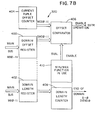
- the min/max module 320 included in an ADC, like 306, is shown in more detail in Figs. 7A and 7B.
- the general function of module 320 is to find the minimum or maximum value of a domain of any qualified tuples in a single pass through a relation. After an associative search of the data in the storage arrays like 310, the answer or selected data is returned to the PFP 304 (Fig. 1) for comparison with data from other ADCs.
- Figs. 7A and 7B show more details of the min/max module 320; however, it is difficult to completely explain the operation of this module without having to explain some of the functioning of the other modules such as the qualify module 322 or the loop control module 328 included within an ADC such as 306. Accordingly, each of the modules such as 320, 322 within an ADC such as 306 will be explained separately, and the cooperation among the various modules will be explained later herein where convenient.
- the min/max module 320 shown in Figs. 7A and 7B includes a buffer A shown as block 386 and a buffer B shown as block 388.
- the buffer A initially holds the comparison argument, and the buffer B is used to hold the domain currently being read. Because a decision with regard to the domain being read cannot be made until the entire tuple has been read, the buffer B will be loaded once during each tuple read. In searching for a minimum, for example, if a value like V 1 is found in buffer B which value is lower than the value initially entered into buffer A, then the buffers A and B switch functions and buffer B becomes the buffer in which the new argument (value V 1 ) is stored and buffer A becomes the buffer in which the data from the storage array is entered to repeat the process.
- one of the buffers, A or B becomes the reference buffer and the other one is continually updated; this process of shifting functions continues until a final minimum, for example, is found.
- Each one of the buffers A or B has an indicator associated therewith to indicate which one of the buffers has the final minimum value therein. This final minimum is then routed to the PFP 304.
- the data select block 390 (Fig. 7A) is used to receive data which represents an initial argument for comparison in the min/max module 320.
- data to be selected may be a value which is less than 5.
- This data select is initiated on the keyboard 340 (Fig. 5) associated with the access control unit 302 and routed over the main bus lines MB ⁇ -7 to the data select block 390.
- the address counter block 392 is used to supply an address to both buffer A and buffer B regardless of which function they are performing.
- There are two data select blocks 394 and 396 (Fig. 7A) which pick out whether it was buffer A or buffer B which contained the minimum value to be fed out the main bus MB ⁇ -7 to the PFP 304.
- the data compare block 398 is what is used to find the new minimum (or maximum) by comparing data from the storage array (like 310) coming over bus lines CRD0-7.
- Fig. 7B shows in very general form, the logic which is used to find domains within a tuple; essentially this is found by a byte offset count and a length.
- the relational model shown in Fig. 4 is organized with domain #2 starting at an offset of 6 bytes, i.e., the first byte of domain #2 begins after byte 1-6, and the length of domain #2 is 4 bytes long, extending from byte 2-1 through byte 2-4. Proceeding with the example given, if the minimum function were being searched, and the data being searched were located in domain #2, the offset of 6 bytes would be placed in the domain offset register 400 via the main bus, and the domain length of 4 bytes would be placed in the domain length register 402.
- a current tuple offset counter 404 is reset to 1, in the illustration in Fig. 4, and is incremented as each byte is searched; consequently, when the count in the counter 404 reaches six (in the illustration given), the domain offset register 400 and the counter 404 would have the same count (7), indicating that this next byte (2-1) is the start of domain #2.
- the output of the counter 404 (Fig.
- the min/max module 320 can pick out a domain within a tuple by testing for an equal on a "compare" of the domain offset, and the min/max module 320 functions until the domain length counter 408 goes to zero, thereby indicating the end of the interested domain. The entire sequence is then started again for each succeeding tuple within the particular relation.
- Figs. 8A and 8B show more details of the qualify module 322 which is part of an ADC 306 shown in Fig. 3.
- the qualify module 322 determines whether or not a particular tuple from a storage array 310 matches the tuple select criteria issued to this module 322.
- up to 16 domain fields within each tuple may be used as a basis for selection.
- the qualify module 322 (Figs. 8 A and 8B) includes a tuple offset counter 418 (which is similar to the tuple offset counter 404 in Fig. 7B) and a domain start comparator 420 which is similar to the offset comparator 406 included in the min/max module 320 shown in Fig. 7B.
- the module 322 (Fig. 8A) also includes a domain start file 422, a domain length file 424, a domain valid file 426 and a domain condition file 428, with each one of these files containing 16 values, one for each domain in use within a tuple.
- the domain start file 422 contains the byte offset at the start of the domain selected
- the domain length file 424 contains the number of bytes in the domain
- the domain valid file 426 contains a bit representing that the above information is currently in use
- the domain condition file 428 contains a four bit field which selects the correct relational operator.
- the qualify module 322 (Figs. 8A, 8B) also includes an argument buffer 430 (Fig. 8B) which contains the reference values for the valid domains as a string of bytes with the most significant bit (MSB) of the first domain being first, the MSB of the second domain following the least significant bit (LSB) of the first domain and so on as previously described in relation to Fig. 4.
- the argument buffer 430 holds a maximum of 256 bytes.
- a byte as used herein is comprised of 8 bits.
- the qualify module 322 (Figs. 8 A, 813) also includes a domain counter 432, a domain length counter 434, an argument address counter 436, a domain comparator 438, a tuple comparator 440, compare decision logic 442 and a tuple OR/AND select unit 444.
- the general functioning of the qualify module 322 shown in Figs. 8A and 8B is as follows. At the start of a tuple, the tuple offset counter 418, the domain counter 432 and the argument address counter 436 are cleared or reset to zero. The tuple offset counter 418 is incremented each time a byte is read from the storage array 310. When the output of the domain start file 422 is equal to the output of the tuple offset counter 418 and the output of the domain valid file 426 is a "one" (indicating that a qualify test is desired) the domain length counter 434 is loaded with the output of the domain length file 424 and the domain comparator 438 is enabled.
- the domain length counter 434 is decremented by one, the argument address counter 436 is incremented by one, and the output of the domain comparator 438 is updated until the output of the domain length counter 434 is equal to zero; then the domain counter 432 is incremented and the output of the tuple comparator 442 is updated.
- the output of the tuple comparator 440 indicates whether or not the tuple qualified.
- the domain start comparator 420 compares the current tuple offset (which is a byte count) with the desired offset that the qualify module 322 is looking for; if they are equal, then the start domain sequence signal (STDOM) is outputted from the comparator 420 and it indicates to the compare decision logic 442 to start comparing because the data from the storage array 310 is presently at the domain being searched. The comparison continues at the domain comparator 438 until the domain length counter 434 goes to zero which indicates that all of the bytes of the domain of interest have been compared with the argument data. Because there are 16 addresses or offsets and 16 lengths in the domain start file 422 and the domain length file 424, respectively, there are also 16 bits in the domain valid file 426 which correspond to each of the 16 addresses or offsets.
- a VALID signal is outputted from the domain valid file 426 to the compare decision logic 442.
- the actual comparison is done by the domain comparator 438; one of the inputs to the comparator 438 handles the data from the storage array 310 and the other input for the comparison comes from the argument buffer 430.
- the address for the argument buffer 430 is supplied by the argument address counter 436. For example, if one wanted to access data associated with a Social Security No. 511 50 1444, then this number would be placed in the argument buffer 430, and when the domain having that Social Security No. was available from the storage array 310, the comparison would take place on a byte level for a match. In the embodiment described, there can be up to 16 arguments in the argument buffer 430 which match or equal the 16 possible domains to compare in the qualify module 322.
- the module 322 also includes a tuple OR/AND select module 444 (Fig. 14A). The module 444 is used, for example, in a qualify-type statement such as, "If A is true, or B is true, select this tuple".
- the module 444 has AND and OR logic included therein.
- Figs. 10A and 10B show more details of the tag module 324 (Fig. 3) which is part of the ADC 306.
- the basic functions of the module 324 are to:
- the 8 bit byte may be organized as shown in Fig. 11, with bits A-F used for certain tagging functions and bits 7 and 8 being used for certain functions to be later described herein.
- the tag byte designated generally as 450 in Fig. 11 is not shown in the relation shown in Fig. 4, the tag byte may be considered as being in domain #4 -(not shown) for each of the tuples shown in Fig. 4; that is, the 8 bit tag byte 450 would be located in byte 4-1 for each of the tuples shown, with byte 4-2 for each of the tuples being vacant.
- a request to the system may be; "Provide a list of all the people who live in Wichita”. Once the list is prepared, the data is returned to the storage array 310. If at a later time, this same request is required, the same associative match must be made again. If this request for people who live in Wichita is made frequently enough, one of the tag bits A-F in Fig. 11 may be used to indicate the fact that the tuple contains data for a person living in Wichita.
- the tagging provides a method of selecting data in one operation for use in an operation at a subsequent time.
- Fig. 1QA shows the circuitry used for tag comparison
- Fig. 10B shows the circuitry used for tag modification. It appears appropriate to discuss tag modification first.
- Bits 7 and 8 in the tag byte 450 are used for physical and logical deletion, respectively, of records within the storage array 310; i.e. these bits are used in a "transaction-backout"-type situation in which an individual has started a transaction which actually deletes data and later realizes that this was in error. For example, when bit 8 is a binary "0" it indicates that the associated tuple is in the data base and contains valid information or data. When bit 8 is a binary "1", it indicates that the tuple does not contain .useful data and accordingly, the space occupied by this tuple may be used for adding new data therein.
- bit 7 When bit 7 is a binary "0”, it indicates that the associated tuple contains valid data and is included in the data base, and when bit 7 is a binary "1", it means that the data for the associated tuple has been logically excluded from the data base.
- a difference between the physical and logical delete tag bits (bits 8 and 7) is that a tuple may be logically deleted by a binary "1” in bit 7, but the tuple could not be written over; however, with the physical delete tag bit, a binary "1” in bit 8 would mean that the associated tuple does not contain valid data and accordingly can be "written over”. Changing the logical delete bit 7 from a binary "1" to a binary "0” causes the associated tuple to appear in the data base without any of the physical data being lost.
- F ig. 1QB shows the circuitry for changing the tag bits in the tag byte for selected tuples.
- the tag byte for a tuple from the storage array 310 may have the "old field" designation shown ( F ig. 10B) with the bits #1 through #8 being numbered from right to left.
- F ig. 10B the "old field” designation
- a binary "1” would be placed in the second position and the fourth position bits of the tag replacement bit control register 454 as shown by the "change bits”.
- the "old field" from the array 310 will have the bits #2 and #4 (from the “change bits") changed to the values shown in “new bits” ,for these positions to produce the "new field” which is outputted from the 8 channel independent multiplexer 456 . Because a binary "0" already existed in the 4th position of the old field, no change is made in the "new field”. Because a binary "0” existed in the 2nd position of the "old field", and the "new bits” indicate a binary "1” should be in this position (according to the " change bits”, a binary "1” in the second position is the net change in the "new field” compared to the "old field”).
- Fig. 10A shows how the various tuples are tested in order to provide a selection of the data using the tagging technique discussed in relation to Fig. 10 B .
- a typical request to the ADC 306 may be, "Provide the tuples in which the name equals "Smith” and tags #1 and #3 or tags "A" and "C” (Fig. 11- are "on”.
- the circuitry shown in Fig. 10A operates similarly to that associated with the qualify module 322 in that a test is made on each affected tuple to indicate whether or not a match was made.
- the "test bits" having the pattern given in Fig.
- 10A would be placed in a tag qualification mask register 458 and logically ANDED via the block 460 with the "incoming tag" from the associated tuples from the storage array 310.
- the "bits to match” in the example are stored in the tag qualifi--cation match register 462. From Fig. 10A, it can be seen that bits #1 and #3 are to be matched, the remaining bits being "don't care” bits; this means the tags #1 and #3 should be binary "1's" to have the associated tuple selected or qualified.
- the outputs from the logical AND block 460 and the register 462 are fed into a comparator 464 which produces a tag qualified signal (TGQAL) when a match is made.
- TGQAL tag qualified signal
- the qualified tuple is then routed back to the access control unit 302 in Fig. 5 (via the PFP 304) as previously explained.
- the bits 2 -and 4-8 in the incoming tag are not involved in the comparison in comparator 464 because they were not part of the "test bits" forming the basis for comparison ,which test bits are entered into the register 458.
- the read/write module 326 (Fig. 3) included in the ADC 306 is shown in more detail in Figs. 12 A and 12B.
- the general purpose of module 326 is to temporarily hold all data as it is put into and retrieved from the storage array 310.
- the read/write module 326 has the ability to locate up to 16 individual domains within a tuple, and the location logic is similar to that employed for the same function associated with the qualify module 322.
- the current tuple offset is compared to the desired tuple offset to determine the start of a domain as previously explained.
- the length of the domain is known and is kept track of by loading and thereafter decrementing a count.
- a register also contains the number of domains in use so that invalid offsets and lengths are not used.
- the read/write module 326 (Fig. 3) is shown in more detail in Figs. 12A and 12B.
- the domain location circuitry 464 shown in Fig. 12B is similar to the domain location circuitry already described in relation to the qualify module 322 shown in Figs. 12A and 12B.
- the function performed by the domain location circuitry 464 is common to the read/write module 326, the qualify module 322, and the min/max module 320 already described; this function is not needed in the tag module 324 because the tag byte is located in the last domain in a tuple as already discussed in relation to Fig. 11.
- the basic function of the read/write module 326 is to take data via an ADC like 306 (Fig. 1) and place it in the storage array 310, and also, to take data from the array 310 and pass it through the ADC like 306 and return it to a user of the system 300.
- a data select circuit 466 ⁇ Fig. 12A
- a data select circuit 466 provides the selection of the desired domains via the main bus 334, and the data from the storage array 310 passes therethrough via the bus 330. If several domains are to be retrieved, they would be stored in a data RAM 468 and transferred on the main bus 334 to the user of the system 300.
- the data is temporarily stored in the RAM 468 because of the fact that data is available to the ADC like 306 in a sequential manner.
- the data that one wanted to read out may be available before one is aware of the fact that the tuple being read contains the data desired to be read; it is possible that the qualifying is done on a last domain within a tuple and the desired domain to be read is actually the first domain within the tuple.
- a cursory look at the general arrangement of the domains within the tuples shown in Fig. 4 should make this more readily understandable.
- a RAM address counter 470 (Fig. 12A) provides addresses for the data RAM 468 during write and read operations.
- the data comes from the main bus 334 (Fig. 12A) and passes through the data select 466 to the data RAM 468.
- the data to be written is transferred from the data RAM 468 through a buffer 472 to a loop buffer (associated with the loop control module 328) to the storage array 310.
- Data which is read from the storage array 310 passes through the data RAM 468 and through the buffer 473 to the main bus 334.
- a data in storage counter 474 is used to simply keep track of the amount of data in the data RAM 468.
- the capacity of the RAM 468 is 4K bytes; consequently, during a read operation, the counter 474 keeps track of how many bytes of information have been transferred thereto and how many are to be transferred to the PFP 304 (Fig. 1).
- the read/write module 326 writes into the storage array 310. It should be recalled from the discussion made earlier herein with regard to the tag module 324 that some of the tuples within a relation will have valid data in them and some will be marked deleted. An insert of data by the read/write module 326 can occur only in a deleted tuple space. Also, deleted tuples can occur anywhere in the storage array 310 within the pertinent relation. While it doesn't matter which deleted tuple gets filled with data to be written in, it is important that this data have the same format or organization of the domains within a tuple, For example, if a name field or domain within a tuple (see Fig. 4) is four bytes long, the name to be inserted would also have to be arranged in this same format. During a write operation there are three operations which occur simultaneously, namely:
- Fig. 12B contains the domain location circuitry 464 alluded to earlier herein; this circuitry is similar in function to that already discussed in relation to the qualify module 322.
- the domain location circuitry 464 includes a current tuple offset counter 476, a domain offset register file 478 which receives data from the main bus 334 and bus 332, an offset comparator 480, a current domain in use identifier counter 482, a domain length register file 484 which receives data from the main bus 334 and bus 332, a domain length counter 486, and a number of domain fields in use counter 488.
- the general operation of the domain location circuitry 464 shown in Fig. 12B- is as follows.
- the basic function of the domain location circuitry 464 (Fig. 12B) is to enable and disable the operation of the read/write module 326 based on whenever the domain one is interested in is currently available on the data bus. It has a domain level off-on switch.
- the "on" condition is signified by ENOP Enable Operation; this is the signal which starts the read/write module 326 when the first byte of the domain is found.
- the offsets and the lengths of the domains that one is going to look at are stored in the domain offset register file 478 and the domain length register file 484, respectively.
- the count or number in the current domain in use counter 482 provides an address to select a pair of these values sequentially so that one can look at many domains within a tuple.
- the delay offset register file 478 and the current tuple offset counter 476 there must be a match between the delay offset register file 478 and the current tuple offset counter 476.
- the tuple offset counter 476 increments for each byte which comes in. Eventually, one should get a match between the domain offset register file 478 and the tuple offset counter 476.
- the loop control module 328 (Fig. 3) is shown in more detail in Figs. 13A and 13.B. Before discussing the details of the module 328, it appears appropriate to discuss the general functioning thereof.
- the min/max module 320 (Fig. 3), the qualify module 322, the tag module 324 and the read/write module 326 all receive data from the storage array 310 over the bus 330 at the same time; each one of the modules mentioned makes a decision as to whether or not it wants to do anything with the data.
- Th.e loop control module 328 has a loop buffer 490 (Fig. 13A) included therein, and in the embodiment being described, it is a 4K byte buffer. There are two general reasons for having the loop buffer 490.
- the first is that the storage arrays 310 (to be later described herein) include charge coupled devices (CCDs) laid out with 4K bytes of data in one circular path.
- CCDs charge coupled devices
- the other reason is that data is available to all the modules 330, 322, 324, and 326 at the same time, and due to the sequential nature of the operation, one may have to modify or change, for example, a first domain within a tuple but the qualifying is done on the last domain within the tuple. In other words, the domain which is to be modified is presented first, and it is gone by the time one realizes that it is the one to be modified. Therefore, the loop control module 328 makes a temporary modification to the data and stores it in the loop buffer 490 in the modified state.
- the loop control buffer 490 has a number pf tuples that have been modified and are stored there awaiting a decision as to whether or not they should be put back or re-written into the storage array 310. If a particular tuple is qualified and a change was made in it, then that tuple is replaced and the revised tuple is placed back in the storage array 310.
- the loop buffer 490 (Fig. 13A) is a "rollover" or “endless” type buffer in that there appears to be no end to it.
- the loop buffer 490 is of the dual ported storage type in that data can be read from the storage array 310 and written into the storage array 310 at the same time; however, in the embodiment described there is a lag of 4K bytes. In other words, one can read and write effectively at the same time if the read and write points differ by 4K bytes (in the embodiment being described) or a 4K byte address offset. This allows the ADC's such as ADC 306 to read and write simultaneously in parallel.
- Fig. 14 shows one embodiment of how the storage array 310 is organized.
- the storage array 310 is composed of blocks 492, 494, 496,...498 of storage elements, with each block such as 492 being comprised of 64K bytes of storage or 8 chips of CCDs with 64K bits of storage.
- Each of the blocks like 492 is composed of 4K loops such as loop 500.
- 4K bytes of data are read from loop 500 of the block 492, they are temporarily stored in the loop buffer 490 as previously discussed.
- the next data to be read comes from loop 502 from block 494, and because this 4K bytes of data must also be stored in the loop buffer 490, the data which is presently in the loop buffer 490 will be written into the loop 500 of block 492.
- the first byte of data from loop 502 is read into the loop buffer 490, the first byte of data from loop 500 is written back into the first loop 500 of block 492. So, as data is written back into the array 310, it does not change its location or address within the array.
- the 4K loop 504 from block 496 is read into the loop buffer 490, the 4K loop 502 which is stored in the loop buffer 490 is written back into the loop 502 in block 494.
- the transfer from one block of storage from loop 502 to loop 504 or from loop 506 to loop 508 is transparent; no special action is required for the transferrence or sequencing.
- 4K (actually 4096) is simply subtracted from the current read address.
- the relation address is set up in the relation address counter 510 (Fig. 13 ' A) to indicate the start or location of the area of the storage array 310 to be scanned.
- the relation length counter 512 is also supplied with a count (via the main bus 334) which represents the length of the associated relation in bytes of data.
- Each byte of data which is read from the storage array 310 decrements the relation length counter 512, and when the count therein is equal to zero, it indicates the end of the scan.
- the relation address counter 510 also provides addressing for the loop buffer 490 via the adder 514.
- the purpose of the adder 514 is to provide a read look ahead on the storage array 310 in order to manage the loop buffer 490.
- a read data latch 516 (Fig. 13A).
- the output from the latch 516 is sent over the currently read data (CRD) bus (also marked as bus 330 in Fig. 3) to each of the modules 320, 322, 324, and 326 shown in Fig. 3 for operating on the data.
- CCD currently read data
- This data is also selected by the data select block 518 (Fig. 13A) to be read into the loop buffer 490; this is in the case of no modification to the data being read or scanned.
- the data select block 518 will take the new or modified data from the WDB ⁇ -7 bus designated as 520 and the modified data will be written into the loop buffer 490.
- data which is not being modified comes from the array (via latch 516) and data which is being modified comes over the bus 520.
- data which is to be written back into the storage array 310 from the loop buffer 490 it passes through the write data latch 520.
- the loop control module 328 also performs certain bookkeeping functions associated with the ADC 306; most of these functions can be described in relation to the circuitry shown in Fig. 13B.
- the length of the desired tuple is fed to the register 522 (Fig. 13B) via the main bus 334; this allows the loop control module 328 to keep track of tuple boundaries.
- the loop control module 328 modifies or changes data in the storage array 310 by tuple, not by domain. It is possible to have tuples extend across loops such as 502 and 504 in Fig.
- TAGFG tag flag
- RBLANK read blank
- WTAG write tag
- WBLANK write blank
- the WTAG signal from the tuple write counter 526 is true, it means that the current byte being written into the storage array 310 is a tag byte.
- the signals RBLANK and WBLANK have similar meanings except that they mean it is the end of a tuple.
- An initial write delay block 528 (Fig. 1 3 B) is utilized for providing an initial 4K byte delay to enable 4K bytes of data to be written into the loop buffer 490 (Fig. 13A) before any writing occurs.
- the ADC 306 keeps track of modifications to the storage array 310 on a tuple basis, by a write decision RAM 530.
- the RAM 530 in the embodiment described, is a 1K x 1 R A M which contains ⁇ 's or 1's depending upon whether the associated tuples are not to be modified or are to be modified, respectively. In other words, once it is decided that a tuple is to be modified, a "1" is placed in the RAM 530 in a location which corresponds to the associated tuple. When the associated tuple is to be placed back into the storage array 10, the associated bit in the RAM 530 would be a binary "1".
- a count of tuples read counter 532, a count of tuples written counter 534, and a tuple decision RAM address select block 536 are used.
- the associated binary "0" or "1" discussed earlier herein is written into the RAM 530 via the present tuple decision (WRTDCS) signal on line 538.
- the RAM 530 is 1K by 1 bits long and since the loop buffer 490 (Fig. 138).
- 13A is 4K bytes long, it means that each tuple will have at least 4 bytes of data therein, although the size of the RAM 530 and the organization of data in the storage array 310 can be changed to suit particular applications.
- the count of tuples read counter 532 the least significant bits of the count indicated therein are used as an address to write the associated qualifying bit into the RAM 530, and similarly, the count which appears oh the counter 534 is used as an address into the RAM 530 to pick out the associated qualifying bit which was written therein at an address dictated by the counter 532.
- Another feature of the system 300 is that it is not necessary to go through the process stated in the previous paragraph if there are no more tuples to be written back into the storage array 310 for a particular relation.
- a count of pending tuples to be written is maintained in a counter 540 (Fig. 13B).
- the counter 540 is incremented whenever a tuple needs to be written back into the storage array 310 and it is decremented each time a tuple is written therein.
- a conventional latch 542 is used to latch the output from the RAM 530 for the qualifying bits coming therefrom.
- the various signals shown in Figs. 13B and 13A will be discussed in detail hereinafter.
- An address buffer 544 (Fig. 13 A) is used to provide the addresses to the storage array 310.
- a hit counter 546 is used to count the number of tuples which have met various selection criteria, as for example, "the number of people who live in Wichita" as earlier discussed herein. Such a count is sent along the main bus 334 to the PFP 304 (Fig. 1) where similar counts from other ADCs, like 308, can be added together to obtain a composite count for the system 300.
- loop control module 328 shown generally in Figs. 13A and 13B, an explanation of the associated control signals and the detailed circuitry used therein will now be discussed.
- the read data latch 516 (Fig. 13A) is comprised of a conventional latch H9 (Fig. 15A) such as IC #LS374 which is manufactured by Texas Instruments, Inc. which will be hereinafter referred to as T.I.
- Conventional inverters shown generally as blocks F9 and G9 are used between the DO ⁇ /-D07/ lines (coming from the storage array 310 1 and the inputs to the latch H9.
- the outputs (CRD ⁇ -CRD7) from the data read latch H9 are fed into the data select block 518 (Fig. 13A).
- the data select block 518 (Fig. 13A) is shown in more detail in Figs. 16A and 16B. and it includes the multiplexers K6 and L6 which are conventional IC chips chips such as #LS157 which are manufactured by T .I. for example.
- the CRD ⁇ -CRD3 lines and the new data lines WDB ⁇ through WDB3 lines are handled by the multiplexer K6 (Fig. 16A) and the remaining lines are handled by the multiplexer L6 as shown in Fig. 16B.
- the conventional flip flops D7 and T5 (Fig. 16A) and the gate S7 are used in the development of the control signals used to select the data either from the storage array 310 or the new data to be written therein as previously explained.
- the loop buffer 490 (Fig.
- 13A is a conventional loop buffer such as IC chip #93471 which is manufactured by Fairchild, and is comprised of the select block and the memory units B6, (Fig.. 16A) C6, D6, E6, F6, G6, H6, and J6 shown in Fig. 16B, whose outputs are connected to the conventional latches A5 and A6 (Fig. 16 B ) which comprise the write data latch 520 shown in Fig. 13 A.
- the following List #2 is a list of the inputs and outputs (and the descriptions thereof) associated with the loop control module 328 and shown in Figs. 16A and 16B.
- Each ADC such as 306 (Fig. 3), has control logic designated generally as 548 associated therewith.
- the control logic 548 is divided generally into three logic sections 550, 552 and 554 shown in Figs. 17, 18, and 19, respectively.
- control logic section 550 (Fig, 17) is to generate the count enable to array signal (CNTEN) (Fig. 20); this signal is generated if:
- control logic section 552 (Fig. 18) is to:
- control logic section 554 (Fig. 19) is to produce the QALDC signal which is used to increment the count of tuples pending in the loop buffer 490 (Fig. 13A) and to store the update bit in the write decision RAM 530 (Fig. 13B) of the loop control module 328.
- An update or a qualified hit occurs during any of the following functions:
- a qualified hit means that the tag field and any domain under examination match the data request.
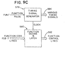
- Fig. 9 A shows a portion of the data interchange module 336 (Fig. 3) and includes a timing signal generator 556, a clock generator 558, and request acknowledge logic 560.
- the timing signal generator 556 (Fig. 9 A) utilizes a transfer out pulse TRNOUT/ from the PFP 304 to generate various timing signals associated with the ADC 306.
- the clock generator 558 (Fig. 9 A) is a conventional generator which produces 10MHz and 20MHz square waves to clock the logic associated with the ADC 306.
- the request acknowledge logic 560 (Fig. 9 A) is used for issuing a request signal (REQ/) to the PFP 304.
- a request signal (REQ/)
- SNDMM send min/max signal coming from the control logic 548
- Fig. 9 B shows a data path included in the data interchange module 336 (Fig. 3).
- the data path is 16 or 20 bits wide; however, there are certain registers within the ADC 306 which are only 8 bits wide; consequently, some data “compression and expansion” (with respect to time) is necessary.
- compression it is meant that a 16 bit word, for example, is converted into two 8 bit bytes, with one 8 bit byte following the other, and for “expansion", the converse is meant.
- the data on lines DCB ⁇ -7 would pass through the bus transceiver 561 and the data on lines DCBB-15 (MSD) would pass through the bus transceiver 562 to the data select module 564.
- the data select module 564 selects the most significant byte ie. from DCB8-15 (in bus transceiver 562) and transfers that to the bus transceiver 566 and thereafter, it is placed on the main bus (marked ⁇ -7) at time T 1 and thereafter the least significant byte from bus transceiver 561 passes through the bus transceiver 566 at time T 2 and is placed on the main bus (marked ⁇ -7).
- the first 8 bit byte of data (which is the most significant byte) passes through the bus transceiver 566 (from the main bus ⁇ -7) and is forwarded to the data latch 568, and the second or least significant 8 bit byte passes through the bus transceiver 566 to the data latch 570.
- a 16 bit word is assembled in the data latches 568 and 570, and, consequently, a 16 bit word may be outputted, via the bus transceivers 562 and 561, respectively, to the DCBB-15 and DCB ⁇ -7 data lines.
- the most significant 8 bit byte passes through the bus transceiver 572 to the bus transceiver 562, and similarly, the least significant 8 bit byte passes through the bus transceiver 566 to the bus transceiver 561.
- the timing signal generator 578 and the function decode and latch module 580 shown in Fig. 9C are also part of the data interchange module 336 shown in Fig. 3.
- the (FUN/) signal is fed into the timing signal generator 578 and the specific function code is placed on the FC ⁇ -7 lines leading into the function decode and latch module 580 where that particular function code is latched; the FUN/ signal is used to latch the particular function code in the module 580.
- the function controls lines 582 are utilized to control the movement of data, as for example, from certain registers within the ADC 306.
- the timing signals shown by line 584 are utilized to control certain logic as will be described hereinafter.
- Fig. 20 is a general block diagram showing how an ADC like 306 is interfaced with its associated storage array 310, via its associated array controller 312.
- the storage array 310 is organized as a group of cells in which each cell contains one byte of information and has one parity bit associated therewith.
- the cells are organized into 128 loops of 4096 cells for a total storage capability of 512K bytes in the embodiment described. Within a loop, the cells are accessed serially at a 2MHZ rate.
- Two eight bit paths are provided into the storage array 310; there is one path for reading data and a second path for writing data.
- Data can be simultaneously read from and written into the storage array 310 at the 2MHZ rate; however; the address from which data is read precedes the address into which data is written by 4096 bytes or 4K as it is generally referred to. It should be recalled that 4096 bytes of data were stored in the loop buffer 490 (Fig. 13A to enable the simultaneous reading and writing mentioned.
- the array controller 312 (Fig. 20) contains the necessary clock generation circuits for the CC D s comprising the storage array 310 and for the address control logic associated therewith.
- the CCDs are of the volatile memory type which must be continually shifted to retain the data therein.
- data is loaded into the storage arrays (like 310) from permanent storage devices such as magnetic tapes, discs, etc.
- Each storage array 310 is divided into a data array No. 1 and a data array No. 2 as shown.
- the address lines to the storage array 310 are the MAD ⁇ /-MAD19/ lines, data read from the array 310 passes out of the array to the ADC 306 over the DO ⁇ /-DO ⁇ 7/ lines, and the data written into the array passes over the DI ⁇ /-DI ⁇ 7/.
- the MAD ⁇ / MA D 19/ lines are the address lines; they represent the bvte address received from the ADC's (like 306) for the associated array controller (like 312) to fetch.
- the "read” address which is passed from the ADC 306 to the array controller
- the "write” address is always an implied address which is derived from the read address; ie., the write address is always 4096 bytes less than the read address because of the 4K loop buffer 490 (Fig.13A) mentioned earlier herein.
- the lower 12 bits of the address lines (MAD ⁇ / through MAD11/) are used to select a particular address in a CCD loop mentioned, and the upper 8 bits of the address lines (MAD12/ through MAD19/) are decoded to select a particular chip on a bank of 8 CCDs, with one such bank being shown in Figs. 22A, 22B and 22C.
- the array controller 312 (Fig. 20) is shown in more detail in Figs. 21A and 21B.
- the controller 312 includes an address receiver 548 which receives the MAD ⁇ /-MAD19/ lines, a receiver and driver 550, and controller logic 552.
- the array controller 312 also includes an address counter 556 which is incremented continuously from the time power is turned on in the system 300.
- the counter 556 counts from ⁇ to FFF (in hex designation) to assign an address for the 4K loop mentioned earlier herein, and the starting location of address ⁇ is arbitrarily assigned at power on time.
- the counter 556 is incremented at the same rate as data is shifted in the circular loop of the CCDs; therefore, they stay in synchronization.
- the address latch counter 554 (Fig.
- the 21 A loads therein the 8 most significant bits (MAD11/ to MAD19/) of the match address coming from the A DC 306 upon the occurrence of the load address counter signal LACT/.
- the output from the address counter 556 is fed into the subtraction logic 558 which takes the address from counter 556 and subtracts 4K or 1000 (hex) therefrom to provide the write address to the write address driver-multiplexer 560, which write address is 4096 bytes fewer than the read address to provide for the 4K loop mentioned.
- the upper 8 bits are divided as follows: the lower seven bits from the multiplexer 560 go to a write address driver 562 and the eighth bit goes to a write select board 564 which selects data array #1 or data array #2 of the storage array 310.
- a multiplexer control 566 is used to select either the write address multiplexer 560 or a read address, multiplexer 568 which has associated therewith a read address driver 570 and a read board select 572.
- the array controller 312 also has a clock generator 574 and a parity error indicator 576. A description of the various inputs, outputs and control signals associated with the array controller 312 shown in Figs. 21A and 21B is included in List # 3.
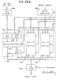
- Figs. 22A, 22B, and 22C taken together show a data array such as array #1 which is part of the storage array 310 as shown in Fig. 2 0 .
- the data array shown in Figs. 22'A-C is substantially conventional and includes a clock receiver 582, a write address receiver 584, a decode and control 586, a read address receiver 588, an in receiver 590 and an out receiver 592.
- Each one of the sections like 578, 580 (Fig. 22A) has the elements shown in the dashed rectangle for section 594.
- the section 594 (Fig. 22A) includes a clock driver 596, an address multiplexer 598, an out buffer 600, and a 64K x 8 CCD array 602.
- the array 602 is arranged in 16 loops of 4K bytes each, and the upper 4 bits from the write address receiver (584 in Fig. 22A), i.e., WAD3/-WAD6/, are used to select the particular one of the 16 loops in the array 602 (Fig. 66A) and the WA ⁇ /-WA2/ lines are used to select a particular section like 578, 580 also shown in Fig. 22A. All of the outputs (shown in List #2 from the array controller 312 become inputs to the storage array 310 with the exception of the DS/ and MMRDY signals shown in this list.
- the data out lines DO ⁇ / through D07/ coming from the out receiver 592 (Fig. 22B) are routed to the associated ADC like 306; receiver 592 is a part of the data array #1 (Fig. 20).
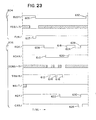
- Fig. 23 shows a group of timing diagrams associated with the transfer of control functions and data between the PFP 304 and the ADC's like 306 and 308 as shown in Fig. 5.
- Fig. 23 along with Figs. 24-28 have the associated signals listed on the left side (as for example the BUSY/ signal in Fig. 23) and each is plotted with respect to time.
- a low level for a signal is considered to be active or true, and a high level for a signal is considered to be inactive or false.
- the BUSY/ signal, the data lines FC ⁇ /-7/, and the function signal FUN/ shown in bracket 604 represent control functions being handled between the PFP 304 (Fig. 5) and the ADC's 306 and 308, for example, with no data being transferred therebetween.
- a function code FUN/
- each of the ADCs will send a busy signal back to the PFP 304 by having the BUSY/ line (Fig. 23) drop to a low level, as at point 605, indicating to the PFP 304 that the function code was received by the ADCs.
- the particular function code is placed on the FC ⁇ /-7/ data lines (also shown as bus 358 in Fig. 5) and transferred to the ADCs like 306 via the FUN/ pulse as at point 607.
- the timing diagrams included in the bracket 606 in Fig. 25 are utilized when data is to be transferred between the PFP 304 and the ADCs like 306 for such functions as READ, MIN, and MAX as earlier explained herein.
- the timing diagrams shown in bracket 604 are also utilized in addition to those enclosed in bracket 606.
- the appropriate function code would be placed on the FC ⁇ /-7/ data lines and the function pulse FUN/ would become active.
- the various ADCs such as 306 and 308 would perform the READ operation until one of them wished to send data to the PFP 304.
- an ADC such as 306 polls the PFP 304 by having the line RQX/ change to an active level as at point 608 in Fig. 23.
- the RQX/ line stands for any ADC and if the ADC 306 were responding, the RQG/ line in Fig. 5 would drop to the low level as shown at point 608 in Fig. 23.
- the PFP 304 would then respond thereto by having the acknowledge line (ACKX/) change to an active level as at point 610.
- ACKX/ acknowledge line
- the ACKX/ line is analogous to the ACK ⁇ / line in Fig. 5 in the example being discussed.
- the ACK ⁇ / signal changing to the active level means that the PFP 304 is ready to receive data from the ADC 306 for a READ operation in the example being described.
- the data to be transferred to the PFP 304 consists of three words, with the first word being placed on the data lines DCB ⁇ /-19/ and being pulsed to the PFP 304 by the first transfer in (TRNIN/) pulse issued by the ADC 306 as shown at point 612 in Fig. 23.
- the second word is placed on the data lines DCB ⁇ /-19/ and is also transferred to the PFP 304 via the TRNIN/ pulse shown at point 614.
- the third word is subsequently, similarly placed on the data lines DCB ⁇ /-19/ and is transferred to the PFP 304 via the TRNIN/ pulse shown at point 616.
- the ADC (like 306) relinquishes its control of the PFP 304 by having its associated request line like RQ ⁇ / in Fig. 5 change to a high level or inactive state as shown by a point such as 618 in F ig. 23.
- the PFP 304 responds to this release of the request line by having the acknowledge line (ACK p in F ig. 5) change to a high level or inactive state as shown by point 620 in Fig. 23.
- ACK p in F ig. 5 acknowledge line
- FIG. 23 also shows (via the request line RQY/) that a second ADC such as 308 may be attempting to gain access to the PFP 304; this is shown by the RQY/ signal becoming active at point 622. However, because the ACKX/ line (for ADC 306) was still active at this time, there was no acknowledge signal (ACKY/) for ADC 308 shown.
- Fig. 23 also shows that after the first ADC 306 had relinquished access to the PFP 304 by the request line RQX/ changing to a high level at point 618, the associated ADC wanted access to the PFP 304 a second time as shown at point 624 in the RQX/ line. Notice at this time, a second ADC as shown at the request line RQY/ had a prior request for access to the PFP 304 and would have had prior access; however, because a cancel function (CAN/) has been initiated by the PFP 304 at point 626, both the requests RQX/ and RQY/ would not be acknowledged and they would return to the inactive states at points 628 and 630, respectively.
- CAN/ cancel function
- the BUSY/ signal would change to the inactive state at point 632 to free the ADCs to perform another function.
- the second request for access to the PFP 304 occurring at 624 in Fig. 23 could very possibly occur for a READ operation; however, for a MIN or MAX operation, only one response from each ADC like 306 or 308 would be logically possible.
- the wait (WAIT/) function is shown as inactive in Fig. 23 however, it will be discussed more accurately with regard to Fig.28 to be described later herein.
- Fig. 24 contains a group of timing diagrams (enclosed in a bracket 633) which depict a situation in which a count function, for example, is initiated and two ADCs respond thereto.
- a function code is placed on the FC ⁇ /-7/ lines by the PFP 304 and is transferred to the ADCs at point 634 of the function line (FUN/) and thereafter the BUSY/ line goes active at point 636.
- two ADCs respond via the request lines RQ2/ and RQ1/ at points 638 and 640, respectively.
- the PFP 304 resolves this dual request by awarding priority to one of the ADCs as previously explained, and in the example shown, the ADC represented by the request line RQ2/ is selected for a response to the PFP 304 by the acknowledge line ACK2/ changing to an active level at point 642.
- the count from the ADC, such as 306 or 308, etc., associated with the request line RQ2/ is then placed on the data lines DBC ⁇ /-19/ and the transfer in (TRNIN/) pulse is changed to an active level at point 644 to transfer the data to the PFP 304.
- the A DC associated with the request line RQ2/ then relinquishes control of the PFP 304 by having the request line RQ2/ change to the inactive state at point 646.
- the standing request for the ADC associated with line RQ1/ is acknowledged at point 648 in this line.
- the associated data is placed on the DBC ⁇ /-19/ lines and transferred to the PFP 304 via the transfer in pulse (TRNIN/) becoming active at point 650.
- the RQ1/ line becomes inactive at point 652
- the ACK1/ line becomes inactive at point 654
- the BUSY/ line becomes inactive at point 656, following the general pattern previously explained.
- the dashed lines 658 and 660 are present only to facilitate alignment of some of the points such as 652 and 654 in Fi g .. 24.
- the BUSY/ line is driven by the ADCs and provides a way of letting the PFP 304 know that all the ADCs are finished with the particular function being executed when the BUSY/ line goes to a high level.
- Fig. 25- shows a group of timing diagrams (enclosed in a bracket 661) associated with the P FP 304 and the ADC's like 306 and 308 for an INSERT function.
- the various signals shown in Fig.25 have already been discussed and the general pattern of operation is similar to that already discussed with relation to Figs. 23 and 69.
- the importance of Fig.25 is that it shows that for an INSERT function or operation, more than one ADC may respond to the function as storage space for data is undoubtedly available in more than one storage array like 310 or 316. This is shown by the request lines RQX/ and RQY/ becoming active at points 662 and 664, respectively; however, only the ADC associated with the request line RQX/ is acknowledged at point 666.
- the PFP 304 knows that the ADC associated with the request line RQX/ has found a space within the storage array (like 310 or 316) to place the data to be inserted and consequently, the cancel function (CAN/) can be initiated at point 668 to prevent the other ADCs like the one associated with the request line RQY/ from being acknowledged. Thereafter, the data is placed in the appropriate storage array associated with the ADC which is acknowledged, as at point 666, and after the data is inserted in the storage array, the BUSY/ signal becomes inactive at point 670. Because of the parallel searching done by the ADCs like 306, 308, etc., an empty tuple in a storage array 310, or 316 can be readily found, and thereafter only a short time is required to write the data into the selected storage array.
- Fig. 26 shows a group of timing diagrams which are included in a bracket 672 and which are associated with the PFP 304 and the ADCs like 306 and 308 for a Tag function.
- the various signals shown in Fig. 26 have already been discussed and the general pattern of operation is similar to that already discussed in relation to Figs. 23-25..
- Fig. 26. shows how data is transferred from the PFP 304 for a Tag function.
- the operational code 44 in hex
- Table 5 listed earlier herein is placed on the FCO/-7/ lines and thereafter the function pulse (FUN/) goes active at point 674 to transfer the operational code to all the ADCs like 306.
- the new tag information in this example has the Data Field Format shown earlier herein (just prior to Table 5), and this format is placed on the DCB ⁇ /-19/ lines and is transferred out to all the ADCs by the transfer out pulse (TRNOUT/) going active at point 676 in Fig. 26.
- the PFP 304 drives the FC ⁇ /-7/, FUN/, DCBO-19/, and TRNOUT/ lines to transfer all the data mentioned to the ADCs like 306.
- the acknowledge (ACK ⁇ /-15/) lines and the busy line (BUSY/) are inactive.
- Fig. 27 shows a group of timing signals which are included in a bracket 678 and which are associated with the PFP 304 and the ADCs like 306 for multiple data transfers to these ADCs.
- the various signals shown in Fig. 27 nave already been discussed and the general pattern of operation is similar to that already discussed in relation to Figs. 23-26.
- Fig. 27 shows the process of sending multiple words of information or data from the PFP 304 to all the ADCs like 306.
- the particular function code for multiple data transfers is placed on the FC ⁇ /-7/ lines and the function (FUN/) pulse is made active at point 680 as previously described.
- Some of the function codes associated with multiple data transfers are the 6C, 80, and A8 codes which are written in Hex form and which are listed in Table 7.
- the first "word" of the particular data to be transferred is placed on, the DCBO/-19/ lines and the transfer out pulse (TRNOUT/) goes active for the first time at point 682.
- the second word of the data is placed on the DCB ⁇ /-19/ lines and the transfer out pulse goes active for the second time at point 684.
- the third word of data is placed on the DCB ⁇ /-19/ lines and the transfer out pulse goes active for the third time at point 686.
- the BUSY/ line and the acknowledge lines ACK ⁇ /-15/ are inactive as data is being transferred to the ADCs like 306 and 308.
- the various signals such as TRNOUT/, CAN/, and FUN/ coming from the PFP 304 are shown as blocks 688, 690, and 692 in Fig. 6B.
- the status request signal (STSRQ/) coming from the PFP 304 (via latch 694) in Fig. 6B is used by the PFP 304 to request status information from the ADCs such as 306 as previously described.
- Fig. 28 shows a group of timing signals which are included in a bracket 696 and which are associated with the PFP 304 and the ADCs like 306 for a Read operation.
- the various signals shown in Fig. 28 have already been discussed and the general pattern of operation is similar to that already discussed in relation to Figs. 68-72.
- an ADC such as 306 or 308 wishes to forward data to the PFP 304 as a result of a Read operation
- its associated request line such as RQ3/
- the PFP 304 acknowledges this request by having the associated acknowledge line (ACK3/) become active as at point 700.
- the busy line (BUSY/) may also be active at this time due to other ADCs being involved in the Read operation.
- the acknowledge line ACK3/ becomes active
- the data which was read is placed on the DCB ⁇ /-l9/ data lines and the transfer in pulse (TRNIN/) becomes active at point 702 to transfer the first byte of information read to the PFP 304.
- the PFP 304 will cause the wait line (WAIT/) to go active at point 704; this prevents the ADCs from sending data to the PFP 304 before the PFP 304 is ready to receive the data.
- the storage arrays like 310 and 316 in Fig.
- the wait line prevents the ADC's like 306 from transferring data to the PFP 304 before it is ready to receive it.
- the wait signal becomes inactive as at point 706 in Fig. 28
- the second byte of data is placed on the DCB ⁇ /-19/ lines and the transfer in line goes active a second time at point 708 to transfer the second byte of data read to the PFP 304.
- the associated request line RQ3/ goes inactive at point 710 and thereafter, the busy line goes inactive at point 712.
Landscapes
- Engineering & Computer Science (AREA)
- Databases & Information Systems (AREA)
- Theoretical Computer Science (AREA)
- Computational Linguistics (AREA)
- Data Mining & Analysis (AREA)
- Physics & Mathematics (AREA)
- General Engineering & Computer Science (AREA)
- General Physics & Mathematics (AREA)
- Information Retrieval, Db Structures And Fs Structures Therefor (AREA)
Applications Claiming Priority (2)
| Application Number | Priority Date | Filing Date | Title |
|---|---|---|---|
| US135792 | 1980-03-31 | ||
| US06/135,792 US4376974A (en) | 1980-03-31 | 1980-03-31 | Associative memory system |
Publications (3)
| Publication Number | Publication Date |
|---|---|
| EP0037264A2 true EP0037264A2 (de) | 1981-10-07 |
| EP0037264A3 EP0037264A3 (en) | 1984-08-22 |
| EP0037264B1 EP0037264B1 (de) | 1986-09-17 |
Family
ID=22469692
Family Applications (1)
| Application Number | Title | Priority Date | Filing Date |
|---|---|---|---|
| EP81301334A Expired EP0037264B1 (de) | 1980-03-31 | 1981-03-27 | Assoziativspeichersystem |
Country Status (4)
| Country | Link |
|---|---|
| US (1) | US4376974A (de) |
| EP (1) | EP0037264B1 (de) |
| JP (1) | JPS56152045A (de) |
| DE (1) | DE3175321D1 (de) |
Cited By (1)
| Publication number | Priority date | Publication date | Assignee | Title |
|---|---|---|---|---|
| AU577396B2 (en) * | 1984-07-31 | 1988-09-22 | Alcatel N.V. | Method for searching an association matrix |
Families Citing this family (10)
| Publication number | Priority date | Publication date | Assignee | Title |
|---|---|---|---|---|
| US5508815A (en) * | 1981-12-14 | 1996-04-16 | Smart Vcr Limited Partnership | Schedule display system for video recorder programming |
| US5168558A (en) * | 1986-01-29 | 1992-12-01 | Digital Equipment Corporation | Apparatus and method for providing distributed control in a main memory unit of a data processing system |
| US4954946A (en) * | 1986-01-29 | 1990-09-04 | Digital Equipment Corporation | Apparatus and method for providing distribution control in a main memory unit of a data processing system |
| US6195738B1 (en) * | 1993-12-12 | 2001-02-27 | Associative Computing Ltd. | Combined associative processor and random access memory architecture |
| US6362990B1 (en) * | 1999-09-10 | 2002-03-26 | Sibercore Technologies | Three port content addressable memory device and methods for implementing the same |
| US6553453B1 (en) | 1999-09-10 | 2003-04-22 | Sibercore Technologies, Inc. | Variable width content addressable memory device for searching variable width data |
| US6392910B1 (en) | 1999-09-10 | 2002-05-21 | Sibercore Technologies, Inc. | Priority encoder with multiple match function for content addressable memories and methods for implementing the same |
| US6483732B2 (en) | 2000-12-13 | 2002-11-19 | Koninklijke Philips Electronics N.V. | Relational content addressable memory |
| DE10256502A1 (de) * | 2002-12-04 | 2004-06-24 | Hyperstone Ag | Speichersystem mit mehreren Speichercontrollern und Verfahren zu deren Synchronisierung |
| US9378782B1 (en) * | 2015-05-24 | 2016-06-28 | Silicon Laboratories Inc. | Apparatus with write-back buffer and associated methods |
Family Cites Families (15)
| Publication number | Priority date | Publication date | Assignee | Title |
|---|---|---|---|---|
| US3448436A (en) * | 1966-11-25 | 1969-06-03 | Bell Telephone Labor Inc | Associative match circuit for retrieving variable-length information listings |
| US3648254A (en) * | 1969-12-31 | 1972-03-07 | Ibm | High-speed associative memory |
| GB1443777A (en) * | 1973-07-19 | 1976-07-28 | Int Computers Ltd | Data processing apparatus |
| FR2271579A1 (en) * | 1974-05-16 | 1975-12-12 | Schlumberger Compteurs | Selector for maximum values of electrical demand - compares first memory with result of second and third memory comparison |
| AT354159B (de) * | 1975-02-10 | 1979-12-27 | Siemens Ag | Assoziativspeicher mit getrennt assoziierbaren bereichen |
| GB1540996A (en) * | 1975-05-12 | 1979-02-21 | Plessey Co Ltd | Associative processors |
| US4130867A (en) * | 1975-06-19 | 1978-12-19 | Honeywell Information Systems Inc. | Database instruction apparatus for determining a database record type |
| SU604033A1 (ru) * | 1975-10-28 | 1978-04-25 | Предприятие П/Я М-5769 | Ассоциативное запоминающее устройство |
| FR2348544A1 (fr) * | 1976-04-15 | 1977-11-10 | Honeywell Bull Soc Ind | Ensemble double de memoire associative |
| US4099242A (en) * | 1976-11-03 | 1978-07-04 | Houston George B | One-pass general associative search processor |
| US4115850A (en) * | 1976-11-03 | 1978-09-19 | Houston George B | Apparatus for performing auxiliary management functions in an associative memory device |
| DE2712575C2 (de) * | 1977-03-22 | 1985-12-19 | Walter Dipl.-Ing. 8011 Putzbrunn Motsch | Assoziatives Speichersystem in hochintegrierter Halbleitertechnik |
| US4145737A (en) * | 1977-04-19 | 1979-03-20 | Semionics Associates | Associative memory device with time shared comparators |
| US4144564A (en) * | 1977-04-19 | 1979-03-13 | Semionics Associates | Associative memory |
| DE3009317C2 (de) * | 1980-03-11 | 1981-11-26 | SIEMENS AG AAAAA, 1000 Berlin und 8000 München | Hybrid-Assoziativspeicher |
-
1980
- 1980-03-31 US US06/135,792 patent/US4376974A/en not_active Expired - Lifetime
-
1981
- 1981-03-27 EP EP81301334A patent/EP0037264B1/de not_active Expired
- 1981-03-27 DE DE8181301334T patent/DE3175321D1/de not_active Expired
- 1981-03-30 JP JP4570181A patent/JPS56152045A/ja active Pending
Cited By (1)
| Publication number | Priority date | Publication date | Assignee | Title |
|---|---|---|---|---|
| AU577396B2 (en) * | 1984-07-31 | 1988-09-22 | Alcatel N.V. | Method for searching an association matrix |
Also Published As
| Publication number | Publication date |
|---|---|
| JPS56152045A (en) | 1981-11-25 |
| US4376974A (en) | 1983-03-15 |
| DE3175321D1 (en) | 1986-10-23 |
| EP0037264B1 (de) | 1986-09-17 |
| EP0037264A3 (en) | 1984-08-22 |
Similar Documents
| Publication | Publication Date | Title |
|---|---|---|
| US4881163A (en) | Computer system architecture employing cache data line move-out queue buffer | |
| US3967247A (en) | Storage interface unit | |
| JPS5830319Y2 (ja) | コンピユ−タシステム | |
| KR950007448B1 (ko) | 집적회로 메모리 시스템 | |
| EP0166310B1 (de) | Datenverarbeitungssystem | |
| US3647348A (en) | Hardware-oriented paging control system | |
| US5347642A (en) | Cache memory management unit | |
| EP0037264B1 (de) | Assoziativspeichersystem | |
| JPH0128412B2 (de) | ||
| US5134711A (en) | Computer with intelligent memory system | |
| US5203001A (en) | Portable computer having an updatable table of starting addresses for accessing those stored programs having been previously executed | |
| JPH04230550A (ja) | 情報処理ネツトワーク及び情報処理方法 | |
| US5404549A (en) | Method for efficient access of data stored in a nexus table using queue tag indexes in a table portion | |
| JPH01118956A (ja) | データ処理装置 | |
| JPH05143451A (ja) | データ処理装置 | |
| JPH0962697A (ja) | 商品コード検索方式 | |
| JP2520941B2 (ja) | デ―タベ―ス・テ―ブルを検索する方法 | |
| JPS62184561A (ja) | 入出力バツフア制御装置 | |
| JPS63280356A (ja) | 仮想ディスク装置のバッファ管理方式 | |
| JPH03225452A (ja) | ビットエンコードデータ処理システム及びデータワードにおいてダグビットをそう入/抽出する処理方法 | |
| JPS6299827A (ja) | バツフア制御方式 | |
| JPH043251A (ja) | 文書検索方法および文書検索処理装置 | |
| JP2636564B2 (ja) | キャッシュメモリのムーブイン制御方式 | |
| JPS633351A (ja) | バツフア検索制御方式 | |
| JPH01134545A (ja) | ブロックデータ転送高速化回路 |
Legal Events
| Date | Code | Title | Description |
|---|---|---|---|
| PUAI | Public reference made under article 153(3) epc to a published international application that has entered the european phase |
Free format text: ORIGINAL CODE: 0009012 |
|
| AK | Designated contracting states |
Designated state(s): DE FR GB |
|
| 17P | Request for examination filed |
Effective date: 19820318 |
|
| DET | De: translation of patent claims | ||
| PUAL | Search report despatched |
Free format text: ORIGINAL CODE: 0009013 |
|
| AK | Designated contracting states |
Designated state(s): DE FR GB |
|
| GRAA | (expected) grant |
Free format text: ORIGINAL CODE: 0009210 |
|
| AK | Designated contracting states |
Kind code of ref document: B1 Designated state(s): DE FR GB |
|
| REF | Corresponds to: |
Ref document number: 3175321 Country of ref document: DE Date of ref document: 19861023 |
|
| ET | Fr: translation filed | ||
| PLBE | No opposition filed within time limit |
Free format text: ORIGINAL CODE: 0009261 |
|
| STAA | Information on the status of an ep patent application or granted ep patent |
Free format text: STATUS: NO OPPOSITION FILED WITHIN TIME LIMIT |
|
| 26N | No opposition filed | ||
| PG25 | Lapsed in a contracting state [announced via postgrant information from national office to epo] |
Ref country code: GB Free format text: LAPSE BECAUSE OF NON-PAYMENT OF DUE FEES Effective date: 19881118 |
|
| GBPC | Gb: european patent ceased through non-payment of renewal fee | ||
| PG25 | Lapsed in a contracting state [announced via postgrant information from national office to epo] |
Ref country code: FR Free format text: LAPSE BECAUSE OF NON-PAYMENT OF DUE FEES Effective date: 19881130 |
|
| PG25 | Lapsed in a contracting state [announced via postgrant information from national office to epo] |
Ref country code: DE Effective date: 19881201 |
|
| REG | Reference to a national code |
Ref country code: FR Ref legal event code: ST |